EP3945142A1 - System und verfahren zur analyse von restgas - Google Patents
System und verfahren zur analyse von restgas Download PDFInfo
- Publication number
- EP3945142A1 EP3945142A1 EP21188172.7A EP21188172A EP3945142A1 EP 3945142 A1 EP3945142 A1 EP 3945142A1 EP 21188172 A EP21188172 A EP 21188172A EP 3945142 A1 EP3945142 A1 EP 3945142A1
- Authority
- EP
- European Patent Office
- Prior art keywords
- processing chamber
- processing
- wafer
- chamber
- gases
- Prior art date
- Legal status (The legal status is an assumption and is not a legal conclusion. Google has not performed a legal analysis and makes no representation as to the accuracy of the status listed.)
- Withdrawn
Links
Images

Classifications
-
- C—CHEMISTRY; METALLURGY
- C23—COATING METALLIC MATERIAL; COATING MATERIAL WITH METALLIC MATERIAL; CHEMICAL SURFACE TREATMENT; DIFFUSION TREATMENT OF METALLIC MATERIAL; COATING BY VACUUM EVAPORATION, BY SPUTTERING, BY ION IMPLANTATION OR BY CHEMICAL VAPOUR DEPOSITION, IN GENERAL; INHIBITING CORROSION OF METALLIC MATERIAL OR INCRUSTATION IN GENERAL
- C23C—COATING METALLIC MATERIAL; COATING MATERIAL WITH METALLIC MATERIAL; SURFACE TREATMENT OF METALLIC MATERIAL BY DIFFUSION INTO THE SURFACE, BY CHEMICAL CONVERSION OR SUBSTITUTION; COATING BY VACUUM EVAPORATION, BY SPUTTERING, BY ION IMPLANTATION OR BY CHEMICAL VAPOUR DEPOSITION, IN GENERAL
- C23C16/00—Chemical coating by decomposition of gaseous compounds, without leaving reaction products of surface material in the coating, i.e. chemical vapour deposition [CVD] processes
- C23C16/44—Chemical coating by decomposition of gaseous compounds, without leaving reaction products of surface material in the coating, i.e. chemical vapour deposition [CVD] processes characterised by the method of coating
- C23C16/4401—Means for minimising impurities, e.g. dust, moisture or residual gas, in the reaction chamber
- C23C16/4405—Cleaning of reactor or parts inside the reactor by using reactive gases
-
- H—ELECTRICITY
- H10—SEMICONDUCTOR DEVICES; ELECTRIC SOLID-STATE DEVICES NOT OTHERWISE PROVIDED FOR
- H10P—GENERIC PROCESSES OR APPARATUS FOR THE MANUFACTURE OR TREATMENT OF DEVICES COVERED BY CLASS H10
- H10P72/00—Handling or holding of wafers, substrates or devices during manufacture or treatment thereof
- H10P72/04—Apparatus for manufacture or treatment
-
- H—ELECTRICITY
- H01—ELECTRIC ELEMENTS
- H01J—ELECTRIC DISCHARGE TUBES OR DISCHARGE LAMPS
- H01J37/00—Discharge tubes with provision for introducing objects or material to be exposed to the discharge, e.g. for the purpose of examination or processing thereof
- H01J37/32—Gas-filled discharge tubes
- H01J37/34—Gas-filled discharge tubes operating with cathodic sputtering
- H01J37/3476—Testing and control
-
- B—PERFORMING OPERATIONS; TRANSPORTING
- B08—CLEANING
- B08B—CLEANING IN GENERAL; PREVENTION OF FOULING IN GENERAL
- B08B13/00—Accessories or details of general applicability for machines or apparatus for cleaning
-
- B—PERFORMING OPERATIONS; TRANSPORTING
- B08—CLEANING
- B08B—CLEANING IN GENERAL; PREVENTION OF FOULING IN GENERAL
- B08B5/00—Cleaning by methods involving the use of air flow or gas flow
-
- C—CHEMISTRY; METALLURGY
- C23—COATING METALLIC MATERIAL; COATING MATERIAL WITH METALLIC MATERIAL; CHEMICAL SURFACE TREATMENT; DIFFUSION TREATMENT OF METALLIC MATERIAL; COATING BY VACUUM EVAPORATION, BY SPUTTERING, BY ION IMPLANTATION OR BY CHEMICAL VAPOUR DEPOSITION, IN GENERAL; INHIBITING CORROSION OF METALLIC MATERIAL OR INCRUSTATION IN GENERAL
- C23C—COATING METALLIC MATERIAL; COATING MATERIAL WITH METALLIC MATERIAL; SURFACE TREATMENT OF METALLIC MATERIAL BY DIFFUSION INTO THE SURFACE, BY CHEMICAL CONVERSION OR SUBSTITUTION; COATING BY VACUUM EVAPORATION, BY SPUTTERING, BY ION IMPLANTATION OR BY CHEMICAL VAPOUR DEPOSITION, IN GENERAL
- C23C14/00—Coating by vacuum evaporation, by sputtering or by ion implantation of the coating forming material
- C23C14/22—Coating by vacuum evaporation, by sputtering or by ion implantation of the coating forming material characterised by the process of coating
- C23C14/54—Controlling or regulating the coating process
-
- C—CHEMISTRY; METALLURGY
- C23—COATING METALLIC MATERIAL; COATING MATERIAL WITH METALLIC MATERIAL; CHEMICAL SURFACE TREATMENT; DIFFUSION TREATMENT OF METALLIC MATERIAL; COATING BY VACUUM EVAPORATION, BY SPUTTERING, BY ION IMPLANTATION OR BY CHEMICAL VAPOUR DEPOSITION, IN GENERAL; INHIBITING CORROSION OF METALLIC MATERIAL OR INCRUSTATION IN GENERAL
- C23C—COATING METALLIC MATERIAL; COATING MATERIAL WITH METALLIC MATERIAL; SURFACE TREATMENT OF METALLIC MATERIAL BY DIFFUSION INTO THE SURFACE, BY CHEMICAL CONVERSION OR SUBSTITUTION; COATING BY VACUUM EVAPORATION, BY SPUTTERING, BY ION IMPLANTATION OR BY CHEMICAL VAPOUR DEPOSITION, IN GENERAL
- C23C16/00—Chemical coating by decomposition of gaseous compounds, without leaving reaction products of surface material in the coating, i.e. chemical vapour deposition [CVD] processes
- C23C16/44—Chemical coating by decomposition of gaseous compounds, without leaving reaction products of surface material in the coating, i.e. chemical vapour deposition [CVD] processes characterised by the method of coating
- C23C16/52—Controlling or regulating the coating process
-
- H—ELECTRICITY
- H01—ELECTRIC ELEMENTS
- H01J—ELECTRIC DISCHARGE TUBES OR DISCHARGE LAMPS
- H01J37/00—Discharge tubes with provision for introducing objects or material to be exposed to the discharge, e.g. for the purpose of examination or processing thereof
- H01J37/32—Gas-filled discharge tubes
- H01J37/32431—Constructional details of the reactor
- H01J37/32798—Further details of plasma apparatus not provided for in groups H01J37/3244 - H01J37/32788; special provisions for cleaning or maintenance of the apparatus
- H01J37/32853—Hygiene
-
- H—ELECTRICITY
- H01—ELECTRIC ELEMENTS
- H01J—ELECTRIC DISCHARGE TUBES OR DISCHARGE LAMPS
- H01J37/00—Discharge tubes with provision for introducing objects or material to be exposed to the discharge, e.g. for the purpose of examination or processing thereof
- H01J37/32—Gas-filled discharge tubes
- H01J37/32431—Constructional details of the reactor
- H01J37/32798—Further details of plasma apparatus not provided for in groups H01J37/3244 - H01J37/32788; special provisions for cleaning or maintenance of the apparatus
- H01J37/32853—Hygiene
- H01J37/32862—In situ cleaning of vessels and/or internal parts
-
- H—ELECTRICITY
- H01—ELECTRIC ELEMENTS
- H01J—ELECTRIC DISCHARGE TUBES OR DISCHARGE LAMPS
- H01J37/00—Discharge tubes with provision for introducing objects or material to be exposed to the discharge, e.g. for the purpose of examination or processing thereof
- H01J37/32—Gas-filled discharge tubes
- H01J37/32917—Plasma diagnostics
- H01J37/32935—Monitoring and controlling tubes by information coming from the object and/or discharge
- H01J37/32981—Gas analysis
-
- H—ELECTRICITY
- H01—ELECTRIC ELEMENTS
- H01J—ELECTRIC DISCHARGE TUBES OR DISCHARGE LAMPS
- H01J37/00—Discharge tubes with provision for introducing objects or material to be exposed to the discharge, e.g. for the purpose of examination or processing thereof
- H01J37/32—Gas-filled discharge tubes
- H01J37/34—Gas-filled discharge tubes operating with cathodic sputtering
-
- H—ELECTRICITY
- H10—SEMICONDUCTOR DEVICES; ELECTRIC SOLID-STATE DEVICES NOT OTHERWISE PROVIDED FOR
- H10P—GENERIC PROCESSES OR APPARATUS FOR THE MANUFACTURE OR TREATMENT OF DEVICES COVERED BY CLASS H10
- H10P72/00—Handling or holding of wafers, substrates or devices during manufacture or treatment thereof
- H10P72/04—Apparatus for manufacture or treatment
- H10P72/0402—Apparatus for fluid treatment
- H10P72/0418—Apparatus for fluid treatment for etching
- H10P72/0421—Apparatus for fluid treatment for etching for drying etching
-
- H—ELECTRICITY
- H10—SEMICONDUCTOR DEVICES; ELECTRIC SOLID-STATE DEVICES NOT OTHERWISE PROVIDED FOR
- H10P—GENERIC PROCESSES OR APPARATUS FOR THE MANUFACTURE OR TREATMENT OF DEVICES COVERED BY CLASS H10
- H10P72/00—Handling or holding of wafers, substrates or devices during manufacture or treatment thereof
- H10P72/06—Apparatus for monitoring, sorting, marking, testing or measuring
-
- B—PERFORMING OPERATIONS; TRANSPORTING
- B08—CLEANING
- B08B—CLEANING IN GENERAL; PREVENTION OF FOULING IN GENERAL
- B08B2205/00—Details of machines or methods for cleaning by the use of gas or air flow
-
- H—ELECTRICITY
- H01—ELECTRIC ELEMENTS
- H01J—ELECTRIC DISCHARGE TUBES OR DISCHARGE LAMPS
- H01J2237/00—Discharge tubes exposing object to beam, e.g. for analysis treatment, etching, imaging
- H01J2237/02—Details
- H01J2237/022—Avoiding or removing foreign or contaminating particles, debris or deposits on sample or tube
- H01J2237/0225—Detecting or monitoring foreign particles
-
- H—ELECTRICITY
- H01—ELECTRIC ELEMENTS
- H01J—ELECTRIC DISCHARGE TUBES OR DISCHARGE LAMPS
- H01J2237/00—Discharge tubes exposing object to beam, e.g. for analysis treatment, etching, imaging
- H01J2237/32—Processing objects by plasma generation
- H01J2237/33—Processing objects by plasma generation characterised by the type of processing
- H01J2237/332—Coating
-
- H—ELECTRICITY
- H01—ELECTRIC ELEMENTS
- H01J—ELECTRIC DISCHARGE TUBES OR DISCHARGE LAMPS
- H01J2237/00—Discharge tubes exposing object to beam, e.g. for analysis treatment, etching, imaging
- H01J2237/32—Processing objects by plasma generation
- H01J2237/33—Processing objects by plasma generation characterised by the type of processing
- H01J2237/334—Etching
Definitions
- Semiconductor fabrication utilizes a variety of processing steps, including etching and depositing films (i.e., layers) on masked wafers in order to create trenches, vias, metal lines, components of passive and active electrical circuits, such as capacitors, resistors, inductors, transistors, antennas, and in general forming insulating and conducting structures in the production of chips having semiconductor integrated circuits.
- etching and depositing films i.e., layers
- components of passive and active electrical circuits such as capacitors, resistors, inductors, transistors, antennas, and in general forming insulating and conducting structures in the production of chips having semiconductor integrated circuits.
- One processing step includes plasma etching performed by applying electromagnetic energy, typically radio frequency (RF), to a gas containing a chemically reactive element, such as fluorine or chlorine.
- RF radio frequency
- the plasma releases positively charged ions that bombard the wafer to remove (etch) materials and chemically reactive free radicals that react with the etched material to form volatile or nonvolatile byproducts.
- the electric charge of the ions directs them vertically toward the wafer. This produces the almost vertical etch profiles essential for the miniscule features in today's densely packed chip designs.
- Process chemistries differ depending on the types of films to be etched. Those used in dielectric etch applications are typically fluorine-based. Silicon and metal etch use chlorine-based chemistries.
- reactive ion etching the objective is to optimize the balance between physical and chemical etching such that physical bombardment (etch rate) is enough to remove the requisite material while appropriate chemical reactions occur to form exhausted volatile byproducts.
- processing steps include non-plasma etching, chemical vapor deposition (CVD) and physical vapor deposition (PVD). These steps, as well as the above-described plasma etching steps, are performed using various precursor gases (i.e., reactive gases and/or reactive gas mixtures, and in some instances, reactive gases and their respective inert carrier gases) provided to a processing chamber that holds the wafers.
- precursor gases i.e., reactive gases and/or reactive gas mixtures, and in some instances, reactive gases and their respective inert carrier gases
- first and second features are formed in direct contact
- additional features may be formed between the first and second features, such that the first and second features may not be in direct contact
- present disclosure may repeat reference numerals and/or letters in the various examples. This repetition is for the purpose of simplicity and clarity and does not in itself dictate a relationship between the various embodiments and/or configurations discussed.
- spatially relative terms such as “beneath,” “below,” “lower,” “above,” “upper” and the like, may be used herein for ease of description to describe one element or feature's relationship to another element(s) or feature(s) as illustrated in the figures.
- the spatially relative terms are intended to encompass different orientations of the device in use or operation in addition to the orientation depicted in the figures.
- the apparatus may be otherwise oriented (rotated 90 degrees or at other orientations) and the spatially relative descriptors used herein may likewise be interpreted accordingly.
- Wafers are often processed in batches, called lots.
- the wafers may be processed in a processing chamber.
- the processing chamber may be temperature and pressured controlled and may include ports for importing precursor (i.e., reactive) gases and exporting byproducts of the processing step, such as any residual gases.
- the processing chamber may also include electronics for creating a plasma of the gases imported to the chamber as part of a processing step. Processing chambers and associated components are well-known in the art and will not be described in greater detail.
- deterioration of the chamber, and specifically the walls of the chamber refers to the buildup of byproducts on the chamber walls, thereby reducing the effectiveness of the respective processing steps that produced such byproducts.
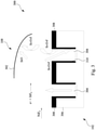
- Fig. 1 illustrates a system 100 for detecting processing chamber condition, according to an embodiment of the disclosure.
- the system 100 includes an ion analyzer module 104 and a process controller 106.
- one or more wafers 102 may be positioned in a processing chamber 108.
- the one or more wafers 102 may represent a batch of wafers.
- the wafer 102 is not positioned in the processing chamber 108.
- the processing chamber 108 may be used in conjunction with semiconductor fabrication process steps known to those of skill in the art.
- the processing chamber may be used in the fabrication of integrated circuits by performing sequences of processing steps, such as deposition of various layers or films via CVD and/or PVD, plasma and non-plasma based etching, ion implantation and annealing, on batches of semiconductor wafers (also referred to semiconductor substrates).
- the wafers 102 may be formed of any type of substrate material, including semiconductor substrates formed of silicon or gallium arsenide.
- the processing chamber 108 processes one or more batches of wafers, such as the batch of wafers 102.
- a batch of wafers may undergo a plurality of fabrication processing steps in the processing chamber 108.
- an operator may initiate a process to detect the condition of the processing chamber 108 as discussed further below.
- the ion analyzer module 104 is coupled to the processing chamber 108, for example, via a conduit 110 and a port 112 of the processing chamber 108.
- the ion analyzer module 104 is also communicatively coupled to the process controller 106 via either a physical connection, such as a communication cable 114, or via wireless communication 116.
- the ion analyzer module 104 is positioned in the processing chamber 108, and the ion analyzer module 104 communicates with the process controller 106 in the same manner as previously described (i.e. wireless communication or via a physical connection through the port 112 of the processing chamber 108).
- the processor controller 106 is included as a component of the ion analyzer module 104.
- the ion analyzer module 104 includes electronics, such as processors, memory, hard disk, I/O, etc., that perform the functions of the process controller 106, as discussed further below.
- the ion analyzer module 104 is a gas chromatograph configured to analyze gases for ion species.
- the gases may include one or more ion species, such fluoride ions, chloride ions and/or bromide ions.
- the gas chromatograph may be configured to measure the concentration of the ion species in the gases.
- the ion analyzer module 104 includes a gas chromatograph and a mass spectrometer for the identification of ion species and the measurement of their respective concentrations. Gas chromatographs and mass spectrometers are well known in the art and will not be discussed in any further detail.
- the ion analyzer module 104 receives a residual gas from the processing chamber 108 either during the processing of a batch of wafers or during one or more wafer-less processing steps.
- Wafer-less processing steps include any semiconductor processing steps, such as production processing steps used in the processing of batches of wafers being performed in the processing chamber 108 without any wafers in the processing chamber 108.
- the residual gas may contain one or more ion species, such fluoride ions, chloride ions and/or bromide ions, but the scope of the disclosure includes ion analyzer modules configured to analyze the residual gas for ion species produced by any semiconductor fabrication processing step.
- the process controller 106 is configured to receive (or retrieve) the results of the gas analysis performed by the gas analyzer module 104.
- the process controller 106 may include electronics 107, such as microcontrollers, memory, hard disk, and/or I/O (i.e., keypads and displays), etc.
- the display 107 of the process controller 106 displays the results of the ion analyzer module 104 to an operator of the system 100.
- the results may indicate the concentrations of the various ion species measured by the gas analyzer module 104, and as such, indicate the condition of the processing chamber 108 (i.e., the extent of processing chamber condition decay).
- the results may indicate, based upon concentrations of one or more (predefined) ion species being greater than one or more (predefined) respective baseline values, that the processing chamber 108 undergo a cleaning process to remove byproducts accumulated through previous processing steps in the processing of one or more batches of wafers.
- the cleaning process cleans (i.e., removes and/or replaces) byproducts from the inner walls of the chamber in preparation for receiving future batches of wafers for future processing.
- the process controller 106 is optionally coupled to a processing gas module 118 via communication link 120.
- the processing gas module 118 is coupled to the processing chamber 108 via one or more gas conduits 122.
- the processing gas module 118 provides the processing chamber 108 with one or more precursor gases (i.e., gases that may react with one another, the batches of wafers being processed and/or other material target substances (e.g., sputtering materials) placed in the chamber 108, such as material substance 124), as well as any inert carrier gases for assisting the transport of the precursor gases.
- precursor gases i.e., gases that may react with one another, the batches of wafers being processed and/or other material target substances (e.g., sputtering materials) placed in the chamber 108, such as material substance 124
- These reactive precursor gases may be used to etch the wafers 102 and deposit layers of different material compositions on the wafers 102.
- the process controller 106 controls the flow of gases, such as precursor and/or inert gases, from the processing gas module 118 to the processing chamber 108.
- the process controller 106 may control the flow of gases by controlling the release, proportions, flow rates and/or shut-off of the gases from the processing gas module 118.
- the process controller 106 is optionally coupled to a cleaning gas module 125.
- the cleaning gas module 125 provides one or more cleaning gases to the processing chamber 108 via one or more cleaning gas conduits 126 for cleaning the processing chamber 108, such as chamber walls 128.
- the process controller 106 controls the flow (i.e., release, proportions, flow rates and/or shut-off) of the cleaning gases from the cleaning gas module 125 to the processing chamber 108 via communication link 130.
- the cleaning gas module 125 includes, or has access to, gases used for cleaning the chamber 108, such as CFx, C4F8, CO, CHxFy, SF6, C5F8, O2, N2, HeO2, C2F6, Ar.
- gases may also include carbon tetrafluoride, chlorine gases and/or gases such as CH4, NF3 and HBr.
- the process controller 106 is configured to initiate the cleaning process of the process chamber by controlling the flow of the one or more cleaning gases from the cleaning gas module 125 to the processing chamber 108. In another embodiment, the process controller 106 is configured to control the wafer-less processing step being performed in the processing chamber 108.
- the process controller 106 may select one or more processing steps, also referred to as a wafer-less processing steps, to be performed in the processing chamber 108.
- the selection may be based upon the history of fabrication processing steps performed on the batches of wafers in the processing chamber 108.
- the history may be stored in the memory 107.
- the selection is based upon the history of fabrication processing steps performed on the batches of wafers in the processing chamber 108 since the last cleaning of the processing chamber 108.
- an operator selects, via the process controller 106, or in another embodiment via input controls (not shown) on the cleaning gas module 125, the one or more wafer-less processing steps to be performed in the processing chamber 108.
- the processing gas module 118 includes, or has access to, such fabrication processing gases as nitrogen trifluoride, chlorine, hydrogen bromide, silicon hexafluoride and carbon tetrafluoride, singly or in any combination, although the scope of the present disclosure includes all gases and combination of gases used in fabrication processing steps.
- the processing gas module 118 and the cleaning gas module 125 includes (or has access to) separate storage canisters of gas, where each canister contains a single fabrication processing gas.
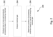
- Fig. 2 is a method flow chart 200 for detecting processing chamber condition, according to an embodiment of the disclosure.
- one or more semiconductor processing steps are performed in a processing chamber 108.
- a process controller 106 may select one or more processing steps (also referred to as wafer-less processing steps) and/or control the flow of one or more gases (e.g., precursor gases and/or inert carrier gases used in the selected processing steps) from the processing gas module 118 to the processing chamber 108.
- the wafer-less processing steps may be based on a history of the processing steps of one or more lots (i.e., batches) of wafers. The history may include the number, types and characteristics, such as precursor gases used and operating parameters of the processing chamber 108, of the previous processing steps performed on more or more batches of wafers.
- an operator may input instructions to an I/O interface 107 of the process controller 106, or alternatively, directly to an I/O interface (not shown) of the processing gas chamber 118 to select one or more processing steps (i.e., also referred to as wafer-less processing steps) and/or to control the release of one or more precursor gases from the processing gas module 118 to the processing chamber 108 based on the results of the ion analyzer module 104 as communicated to the operator by the display 107.
- processing steps i.e., also referred to as wafer-less processing steps
- the one or more wafer-less processing steps includes introducing one or more precursor gases into the processing chamber 108.
- the one or more gases may react with each other, the walls 128 of the processing chamber 108 and/or a target substance (e.g., a sputtering material or the wafer 102) in the processing chamber 108.
- the chemical reaction of the one or more gases with compounds accumulated on the walls 128 of the processing chamber 108 may result in a residual gas.
- the compounds may be accumulated as by-products of the fabrication processing steps performed within the chamber 108 on one or more batches of wafers 102.
- the concentration of one or more ion species in the residual gas indicates the condition of the walls 128 of the processing chamber 108.
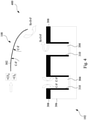
- Fig. 3 illustrates a processing step 300 being performed on the wafer 102 in the processing chamber 108, according to an embodiment of the disclosure.
- the processing step 300 may represent, for example, an etching process, a CVD process, or a PVD process, being performed on the wafer 102 within the processing chamber 108.
- a small segment 302 of the wall 128 of the processing chamber 108 is shown, however the wall 128 of the processing chamber 108 completely encases the wafer 102.
- the processing chamber 108 may be controlled to be at predefined temperatures and/or pressures, and the processing chamber 108 may include electronics, such as electrodes (not shown) for generating a plasma.
- one or more precursor gases are introduced into the processing chamber 108.
- the precursor gases may include, but are not limited to, nitrogen trifluoride, hydrogen bromide and chlorine, sulfur hexafluoride, chlorine, chlorine and sulfur hexafluoride or carbon tetrafluoride.
- the principles discussed below apply to other processing steps such as CVD and PVD for depositing layers on the wafer, and non-plasma based dry etching processing steps using, but not limited to, such precursor gases as xenon difluoride, bromine trifluoride, chlorine trifluoride.
- the processing step 300 is a plasma-based dry etching processing step using nitrogen trifluoride as the precursor processing gas.
- nitrogen trifluoride is provided to the processing chamber 108 for etching trenches 304 in a silicon dioxide film 306 of the wafer 102.
- the wafer 102 has been patterned with a photoresist layer 308.
- a fluorine plasma is generated using RF power applied to electrodes (not shown) in the processing chamber 108, thereby driving a chemical reaction between the nitrogen trifluoride precursor gas and those portions of the wafer 102 not masked by the photoresist layer 308.
- the byproduct of the etching process is silicon tetrafluoride 310, which is a volatile product.
- the plasma in the processing chamber 108 can cause the silicon tetrafluoride to disassociate into free radicals, and the product of this disassociation in the presence of oxygen O 2 can result in a buildup of a layer of silicon oxyfluoride (Si-O-F) compound on the walls 310 of the trench 304 being etched and a buildup of a layer of silicon oxyfluoride, silicon oxide and/or silicon dioxide on the segment 302 of the walls 128 of the processing chamber 108 or on the walls 128 of the processing chamber 108.
- Si-O-F silicon oxyfluoride
- processing steps for providing functional chips (i.e., fabricating functional chips) from a batch of wafers are performed on the batch of wafers (e.g., wafers 102) in the processing chamber 108.
- the thickness of the layer of silicon oxyfluoride compound, for example, and/or other compounds, such as silicon oxide compounds, on the walls 128 of the processing chamber 108 increases.
- a wafer-less processing step such as a wafer-less plasma-based dry etching processing step 300
- the concentration of fluoride ions in the residual gas in the chamber as a result of the chemical reaction between the precursor etching gases and the compounds accumulated on the walls 128 of the processing chamber 108 will be larger when the thickness of the layer of silicon oxyfluoride compound on the walls 128 of the processing chamber 108 is larger, due to more fluorine being available for an oxidation/disassociation plasma-driven process and/or for a bond breaking plasma-driven process in which high energy plasma charged species breaks the bonds of fluorine atoms to other compounds accumulated on the walls 128.
- the measurement of the concentration of fluorine ions in the residual gas is directly correlated to the thickness of the residual compounds accumulated on the walls 128 of the processing chamber 108. That is, a higher concentration of fluorine ions in the residual gas indicate a thicker layer of residual compounds accumulated on the walls 128 of the processing chamber 108.
- the residual gas is analyzed for ion species.
- the ion analyzer module 104 determines the one or more ion species present in the residual gas, including their respective concentrations.
- a condition of the processing chamber 108 is determined based on the analysis of step 204.
- the analysis is performed by the ion analyzer module 104, however in another embodiment, the analysis is performed by the processing controller 106 based upon data received from the ion analyzer module 104.
- the process controller 106 determines that the processing chamber 108 requires a cleaning to remove the layers of processing step byproducts (i.e., residual compounds) accumulated on the walls 128 of the processing chamber 108.
- the indication of a mere presence of a predetermined ion species in the residual gas indicates the processing chamber 108 be cleaned to remove the layers of processing step byproducts accumulated on the walls 128 of the processing chamber 108.
- the process controller 106 upon determining that the process chamber 108 requires a cleaning, automatically controls the flow of cleaning gases from the cleaning gas module 125 to the processing chamber 108 for cleaning the chamber walls 128.
- the process controller 106 includes a display (or an external computer or other processing device includes a display, or an external display is communicatively coupled to the system 100) for displaying the results of the analysis to an operator.
- the operator determines whether to clean the processing chamber 108 based on the results, and the process controller 106 includes an I/O interface 107 for use by the operator to input instructions to the process controller 106 for controlling the flow of cleaning gases for cleaning the processing chamber 108.
- the processing controller is configured to automatically control the flow of precursor gases from the processing gas module 118 to the processing chamber 118, for example by shutting off the flow, and control the flow of cleaning gases from the cleaning gas module 125 to the processing chamber 108 for cleaning the chamber walls 128.
- Fig. 4 illustrates a cleaning process 400 being performed in the processing chamber 108, according to an embodiment of the disclosure.
- one or more cleaning gases are introduced into the processing chamber 108.
- the following discussion depicts a carbon tetrafluoride-based cleaning process, in which carbon tetrafluoride and chlorine gas are introduced into the chamber.
- the scope of the disclosure covers other cleaning gases or mixtures of cleaning gases for removing and/or replacing byproducts of fabrication processing steps, such as the byproducts from etching, CVD and PVD, from the walls 302 of the processing chamber 108.
- a wafer 102 is also shown within the processing chamber 108, in one embodiment of the present disclosure the cleaning process 400 is performed on the processing chamber 108 without any wafers present in the processing chamber 108.
- a fluorine plasma is generated, thereby driving a chemical reaction, in the presence of oxygen, between the cleaning gases and the compounds accumulated on the segment 302 of the wall 128 (or on the walls 128) of the processing chamber 108, such as silicon oxide and/or silicon dioxide (i.e., the silicon oxide compounds).
- the chemical reaction results in replacing the silicon oxide compounds, also referred to as a silicon oxide-based passivation film, on the walls 128 of the processing chamber 108 with a carbon rich layer (C-F), resulting in the production of a volatile silicon oxyfluoride gas (Si-O-F), which can be removed from the processing chamber 108.
- the system 100 may employ artificial intelligence or machine learning techniques that may estimate (e.g., predict), either before a next fabrication processing step or during a fabrication processing step, whether the concentration of one or more ion species of the residual gas is greater than one or more respective baseline values, based upon, for example, residual gas analysis history, fabrication processing history, processing chamber cleaning history, and/or likely future fabrication processing steps.
- the likely future fabrication processing steps may be based upon fabrication processing steps as preprogrammed by an operator of the system 100 and stored in memory and/or based upon fabrication processing history.
- the one or more artificial intelligence or machine learning techniques in some embodiments may be implemented at least in part by machine learning circuitry.
- the electronics of the process controller 106 may include machine learning circuitry that implement one or more artificial intelligence or machine learning techniques.
- Article intelligence is used herein to broadly describe any computationally intelligent systems and methods that can learn knowledge, based upon data history and/or training data, for example, and use such learned knowledge to adapt its approaches for solving one or more problems, for example, by making inferences on the condition of the processing chamber 108, based on received inputs, such as gas analysis (e.g., data corresponding to the measured residual gases) received in real time from the ion analyzer module 104 and/or gas analysis history, fabrication processing history, processing chamber cleaning history, and/or likely future fabrication processing steps retrieved from memory of the process controller 106.
- gas analysis e.g., data corresponding to the measured residual gases
- Machine learning generally refers to a sub-field or category of artificial intelligence, and is used herein to broadly describe any algorithms, mathematical models, statistical models, or the like that are implemented in one or more computer systems or circuitry, such as circuitry of the process controller 106, and which build one or more models based on sample data (or training data) in order to make predictions or decisions.
- the machine learning circuitry of the process controller 106 may employ, for example, neural network, deep learning, convolutional neural network, Bayesian program learning, support vector machines, computer vision, and pattern recognition techniques to solve problems such as predicting or determining the condition of the processing chamber 108. Further, the machine learning circuitry may implement any one or combination of the following computational algorithms or techniques: classification, regression, supervised learning, unsupervised learning, feature learning, clustering, decision trees, image recognition, or the like.
- an artificial neural network may be utilized by the machine learning circuitry to develop, train, or update one or more machine learning models which may be utilized to detect or determine the condition of the processing chamber 108.
- An example artificial neural network may include a plurality of interconnected "neurons" which exchange information between each other. The connections have numeric weights that can be tuned based on experience, and thus neural networks are adaptive to inputs and are capable of learning.
- the "neurons" may be included in a plurality of separate layers which are connected to one another, such as an input layer, a hidden layer, and an output layer.
- the neural network may be trained by providing training data (e.g., past data that are indicative of the condition of the processing chamber 108) to the input layer.
- the neural network may generate and/or modify the hidden layer, which represents weighted connections mapping the training data provided at the input layer to known output information at the output layer (e.g., gas analysis data). Relationships between neurons of the input layer, hidden layer, and output layer, formed through the training process and which may include weight connection relationships, may be stored, for example, as one or more machine learning models within or otherwise accessible to the machine learning circuitry.
- the machine learning circuitry may be implemented in one or more processors having access to instructions, which may be stored in any computer-readable storage medium, which may be executed by the machine learning circuitry to perform any of the operations or functions described herein.
- the present disclosure provides a system and method for detecting processing chamber condition without jeopardizing productions of batches of wafers fabricated in the processing chamber.
- a wafer-less processing step is performed in the processing chamber 108 to determine the condition of the chamber walls 128.
- an operator or a processing controller can determine whether the chamber walls 128 have deteriorated to such an extent as to be cleaned.
- a method for detecting processing chamber condition includes performing a wafer-less processing step in a processing chamber.
- the wafer-less processing step includes introducing one or more precursor gases into the processing chamber.
- the one or more precursor gases react with each other and residual compounds accumulated on the walls of the processing chamber, resulting in a residual gas.
- the method further includes analyzing the residual gas for ion species and determining a condition of the processing chamber based on the analysis.
- a system for detecting processing chamber condition includes an ion analyzer module configured to be coupled to a processing chamber.
- the ion analyzer module is further configured to receive a residual gas from the processing chamber as a result of a wafer-less processing step being performed in the processing chamber.
- the wafer-less processing step includes introducing one or more precursor gases into the processing chamber.
- the one or more precursor gases react with each other and residual compounds accumulated on the walls of the processing chamber, resulting in the residual gas.
- the ion analyzer module further analyzes the residual gas for ion species.
- the system further includes a process controller configured to determine a condition of the processing chamber based on the analysis.
- a computer-readable medium includes instructions executable by a processor for detecting processing chamber condition by performing the step of performing a wafer-less processing step in a processing chamber.
- the wafer-less processing step includes introducing one or more precursor gases into the processing chamber.
- the one or more precursor gases react with each other and residual compounds accumulated on the walls of the processing chamber, resulting in a residual gas.
- the computer-readable medium includes further instructions executable by the processor for detecting processing chamber condition by performing the steps of analyzing the residual gas for ion species and determining a condition of the processing chamber based on the analysis.
- a computer-readable medium comprises instructions executable by a processor for detecting processing chamber condition by performing steps of controlling a semiconductor processing step in a processing chamber, in which the processing step results in the generation of a residual gas in the chamber, analyzing the residual gas for ionic species, and determining a condition of the processing chamber based on the analysis.
- the semiconductor processing step includes introducing one or more gases into the processing chamber. The one or more gases react with each other and residual compounds accumulated on the walls of the processing chamber, thereby generating the residual gas.
Landscapes
- Chemical & Material Sciences (AREA)
- Engineering & Computer Science (AREA)
- Physics & Mathematics (AREA)
- Plasma & Fusion (AREA)
- Analytical Chemistry (AREA)
- Health & Medical Sciences (AREA)
- Epidemiology (AREA)
- Public Health (AREA)
- Chemical Kinetics & Catalysis (AREA)
- Materials Engineering (AREA)
- Mechanical Engineering (AREA)
- Metallurgy (AREA)
- Organic Chemistry (AREA)
- General Chemical & Material Sciences (AREA)
- Drying Of Semiconductors (AREA)
- Formation Of Insulating Films (AREA)
- Physical Vapour Deposition (AREA)
- Chemical Vapour Deposition (AREA)
- ing And Chemical Polishing (AREA)
Applications Claiming Priority (1)
| Application Number | Priority Date | Filing Date | Title |
|---|---|---|---|
| US16/942,577 US11791141B2 (en) | 2020-07-29 | 2020-07-29 | System and method for residual gas analysis |
Publications (1)
| Publication Number | Publication Date |
|---|---|
| EP3945142A1 true EP3945142A1 (de) | 2022-02-02 |
Family
ID=77103966
Family Applications (1)
| Application Number | Title | Priority Date | Filing Date |
|---|---|---|---|
| EP21188172.7A Withdrawn EP3945142A1 (de) | 2020-07-29 | 2021-07-28 | System und verfahren zur analyse von restgas |
Country Status (5)
| Country | Link |
|---|---|
| US (5) | US11791141B2 (de) |
| EP (1) | EP3945142A1 (de) |
| JP (1) | JP2022027596A (de) |
| CN (1) | CN113471096B (de) |
| TW (1) | TWI777291B (de) |
Families Citing this family (2)
| Publication number | Priority date | Publication date | Assignee | Title |
|---|---|---|---|---|
| US11791141B2 (en) | 2020-07-29 | 2023-10-17 | Taiwan Semiconductor Manufacturing Co., Ltd. | System and method for residual gas analysis |
| US12084762B2 (en) * | 2022-05-11 | 2024-09-10 | Taiwan Semiconductor Manufacturing Company, Ltd. | Semiconductor processing tool and methods of operation |
Citations (3)
| Publication number | Priority date | Publication date | Assignee | Title |
|---|---|---|---|---|
| US20030000546A1 (en) * | 2001-05-04 | 2003-01-02 | Lam Research Corporation | Plasma cleaning of deposition chamber residues using duo-step wafer-less auto clean method |
| US7964039B2 (en) * | 2007-09-07 | 2011-06-21 | Imec | Cleaning of plasma chamber walls using noble gas cleaning step |
| US20170282223A1 (en) * | 2016-03-31 | 2017-10-05 | Tokyo Electron Limited | Controlling dry etch process characteristics using waferless dry clean optical emission spectroscopy |
Family Cites Families (22)
| Publication number | Priority date | Publication date | Assignee | Title |
|---|---|---|---|---|
| US5262279A (en) * | 1990-12-21 | 1993-11-16 | Intel Corporation | Dry process for stripping photoresist from a polyimide surface |
| DE4202158C1 (de) * | 1992-01-27 | 1993-07-22 | Siemens Ag, 8000 Muenchen, De | |
| US5679215A (en) * | 1996-01-02 | 1997-10-21 | Lam Research Corporation | Method of in situ cleaning a vacuum plasma processing chamber |
| US6081334A (en) * | 1998-04-17 | 2000-06-27 | Applied Materials, Inc | Endpoint detection for semiconductor processes |
| US6046796A (en) * | 1998-04-22 | 2000-04-04 | Advanced Micro Devices, Inc. | Methodology for improved semiconductor process monitoring using optical emission spectroscopy |
| JP2000348896A (ja) * | 1999-03-26 | 2000-12-15 | Canon Inc | プラズマ発生方法、プラズマ発生装置及びプラズマ反応によるガス処理方法 |
| US6815362B1 (en) * | 2001-05-04 | 2004-11-09 | Lam Research Corporation | End point determination of process residues in wafer-less auto clean process using optical emission spectroscopy |
| US20040235303A1 (en) * | 2001-05-04 | 2004-11-25 | Lam Research Corporation | Endpoint determination of process residues in wafer-less auto clean process using optical emission spectroscopy |
| US7080545B2 (en) | 2002-10-17 | 2006-07-25 | Advanced Technology Materials, Inc. | Apparatus and process for sensing fluoro species in semiconductor processing systems |
| US7312865B2 (en) * | 2004-03-31 | 2007-12-25 | Taiwan Semiconductor Manufacturing Co., Ltd. | Method for in situ monitoring of chamber peeling |
| US8008166B2 (en) | 2007-07-26 | 2011-08-30 | Applied Materials, Inc. | Method and apparatus for cleaning a substrate surface |
| CN101452816B (zh) | 2007-11-30 | 2010-06-02 | 中芯国际集成电路制造(上海)有限公司 | 一种离子注入的监控方法 |
| KR101658975B1 (ko) | 2009-02-11 | 2016-09-23 | 엔테그리스, 아이엔씨. | 반도체 가공 시스템에서의 이온 공급원 세정법 |
| CN103167901B (zh) | 2010-10-25 | 2015-08-19 | 皇家飞利浦电子股份有限公司 | 对真空环境中的分子污染物的分析 |
| CN104736744B (zh) | 2012-10-17 | 2017-06-06 | 东京毅力科创株式会社 | 使用多变量分析的等离子体蚀刻终点检测 |
| US20160320359A1 (en) | 2015-04-29 | 2016-11-03 | Taiwan Semiconductor Manufacturing Co., Ltd. | System and method for monitoring contaminations |
| US9972478B2 (en) | 2016-09-16 | 2018-05-15 | Lam Research Corporation | Method and process of implementing machine learning in complex multivariate wafer processing equipment |
| US10043641B2 (en) * | 2016-09-22 | 2018-08-07 | Applied Materials, Inc. | Methods and apparatus for processing chamber cleaning end point detection |
| US20190093218A1 (en) * | 2017-09-28 | 2019-03-28 | Taiwan Semiconductor Manufacturing Co., Ltd. | In-situ dry clean of tube furnace |
| US20190382889A1 (en) * | 2018-06-15 | 2019-12-19 | Applied Materials, Inc. | Technique to enable high temperature clean for rapid processing of wafers |
| CN120608873A (zh) * | 2018-09-28 | 2025-09-09 | 朗姆研究公司 | 避免沉积副产物积聚的真空泵保护 |
| US11791141B2 (en) | 2020-07-29 | 2023-10-17 | Taiwan Semiconductor Manufacturing Co., Ltd. | System and method for residual gas analysis |
-
2020
- 2020-07-29 US US16/942,577 patent/US11791141B2/en active Active
- 2020-11-12 TW TW109139418A patent/TWI777291B/zh active
- 2020-11-16 CN CN202011277871.XA patent/CN113471096B/zh active Active
-
2021
- 2021-07-28 EP EP21188172.7A patent/EP3945142A1/de not_active Withdrawn
- 2021-07-28 JP JP2021123313A patent/JP2022027596A/ja active Pending
-
2023
- 2023-07-28 US US18/361,771 patent/US12354857B2/en active Active
- 2023-07-28 US US18/361,767 patent/US12176193B2/en active Active
-
2024
- 2024-11-20 US US18/954,223 patent/US20250079142A1/en active Pending
-
2025
- 2025-06-13 US US19/237,982 patent/US20250308868A1/en active Pending
Patent Citations (3)
| Publication number | Priority date | Publication date | Assignee | Title |
|---|---|---|---|---|
| US20030000546A1 (en) * | 2001-05-04 | 2003-01-02 | Lam Research Corporation | Plasma cleaning of deposition chamber residues using duo-step wafer-less auto clean method |
| US7964039B2 (en) * | 2007-09-07 | 2011-06-21 | Imec | Cleaning of plasma chamber walls using noble gas cleaning step |
| US20170282223A1 (en) * | 2016-03-31 | 2017-10-05 | Tokyo Electron Limited | Controlling dry etch process characteristics using waferless dry clean optical emission spectroscopy |
Also Published As
| Publication number | Publication date |
|---|---|
| US20250308868A1 (en) | 2025-10-02 |
| US12176193B2 (en) | 2024-12-24 |
| US20220037137A1 (en) | 2022-02-03 |
| TWI777291B (zh) | 2022-09-11 |
| US20250079142A1 (en) | 2025-03-06 |
| JP2022027596A (ja) | 2022-02-10 |
| US20230386807A1 (en) | 2023-11-30 |
| US11791141B2 (en) | 2023-10-17 |
| US20230386808A1 (en) | 2023-11-30 |
| US12354857B2 (en) | 2025-07-08 |
| CN113471096A (zh) | 2021-10-01 |
| TW202204654A (zh) | 2022-02-01 |
| CN113471096B (zh) | 2025-02-14 |
Similar Documents
| Publication | Publication Date | Title |
|---|---|---|
| US20250308868A1 (en) | System and method for residual gas analysis | |
| JP6615195B2 (ja) | プラズマ処理設備における内表面調整評価のためのシステム及び方法 | |
| US10727073B2 (en) | Atomic layer etching 3D structures: Si and SiGe and Ge smoothness on horizontal and vertical surfaces | |
| US8501499B2 (en) | Adaptive recipe selector | |
| US7456110B2 (en) | Method and apparatus for controlling etch selectivity | |
| US6814814B2 (en) | Cleaning residues from surfaces in a chamber by sputtering sacrificial substrates | |
| JP2024503282A (ja) | 自律型基板処理システム | |
| JPH11145067A (ja) | 半導体素子製造用化学気相蒸着装置及びその洗浄方法並びに工程チャンバーの洗浄工程レシピ最適化方法 | |
| US20120253497A1 (en) | Contact Processing Using Multi-Input/Multi-Output (MIMO) Models | |
| US20120085366A1 (en) | Plasma processing method and plasma processing apparatus | |
| US6335284B1 (en) | Metallization process for manufacturing semiconductor devices | |
| US12412736B2 (en) | Methods and systems for managing byproduct material accumulation during plasma-based semiconductor wafer fabrication process | |
| US20220093429A1 (en) | Systems and methods for determining residual compounds in plasma process | |
| US8945952B2 (en) | High productivity combinatorial workflow for post gate etch clean development | |
| US20260010143A1 (en) | High aspect ratio carbon etch with simulated bosch process | |
| US20240120213A1 (en) | Substrate processing apparatus, substrate processing method and method of fabricating semiconductor device | |
| US20260111005A1 (en) | System and method for plasma pulsing scheme selection and optimization | |
| US20140179112A1 (en) | High Productivity Combinatorial Techniques for Titanium Nitride Etching | |
| WO2025151825A1 (en) | In-situ analysis of metal species for processing chambers | |
| KR20250105750A (ko) | Ai 기반의 반도체 공정 관제시스템 | |
| WO2026019766A1 (en) | High aspect ratio plasma etching with controlled declogging | |
| Tudoroiu et al. | MIMO stochastic minimum variance control strategies for improving plasma characteristics in Reactive Ion Etching | |
| IE83432B1 (en) | Plasma chamber conditioning |
Legal Events
| Date | Code | Title | Description |
|---|---|---|---|
| PUAI | Public reference made under article 153(3) epc to a published international application that has entered the european phase |
Free format text: ORIGINAL CODE: 0009012 |
|
| STAA | Information on the status of an ep patent application or granted ep patent |
Free format text: STATUS: THE APPLICATION HAS BEEN PUBLISHED |
|
| AK | Designated contracting states |
Kind code of ref document: A1 Designated state(s): AL AT BE BG CH CY CZ DE DK EE ES FI FR GB GR HR HU IE IS IT LI LT LU LV MC MK MT NL NO PL PT RO RS SE SI SK SM TR |
|
| STAA | Information on the status of an ep patent application or granted ep patent |
Free format text: STATUS: THE APPLICATION IS DEEMED TO BE WITHDRAWN |
|
| 18D | Application deemed to be withdrawn |
Effective date: 20220803 |