EP3944498A1 - Phase-tracked pulse generation circuit and power supply device - Google Patents
Phase-tracked pulse generation circuit and power supply device Download PDFInfo
- Publication number
- EP3944498A1 EP3944498A1 EP20772727.2A EP20772727A EP3944498A1 EP 3944498 A1 EP3944498 A1 EP 3944498A1 EP 20772727 A EP20772727 A EP 20772727A EP 3944498 A1 EP3944498 A1 EP 3944498A1
- Authority
- EP
- European Patent Office
- Prior art keywords
- circuit
- terminal
- resistor
- power supply
- voltage
- Prior art date
- Legal status (The legal status is an assumption and is not a legal conclusion. Google has not performed a legal analysis and makes no representation as to the accuracy of the status listed.)
- Granted
Links
Images
Classifications
-
- H—ELECTRICITY
- H03—ELECTRONIC CIRCUITRY
- H03K—PULSE TECHNIQUE
- H03K3/00—Circuits for generating electric pulses; Monostable, bistable or multistable circuits
- H03K3/01—Details
- H03K3/012—Modifications of generator to improve response time or to decrease power consumption
-
- H—ELECTRICITY
- H03—ELECTRONIC CIRCUITRY
- H03K—PULSE TECHNIQUE
- H03K5/00—Manipulating of pulses not covered by one of the other main groups of this subclass
- H03K5/22—Circuits having more than one input and one output for comparing pulses or pulse trains with each other according to input signal characteristics, e.g. slope, integral
- H03K5/24—Circuits having more than one input and one output for comparing pulses or pulse trains with each other according to input signal characteristics, e.g. slope, integral the characteristic being amplitude
-
- H—ELECTRICITY
- H03—ELECTRONIC CIRCUITRY
- H03K—PULSE TECHNIQUE
- H03K3/00—Circuits for generating electric pulses; Monostable, bistable or multistable circuits
- H03K3/01—Details
- H03K3/013—Modifications of generator to prevent operation by noise or interference
-
- H—ELECTRICITY
- H03—ELECTRONIC CIRCUITRY
- H03K—PULSE TECHNIQUE
- H03K3/00—Circuits for generating electric pulses; Monostable, bistable or multistable circuits
- H03K3/02—Generators characterised by the type of circuit or by the means used for producing pulses
Definitions
- This application relates to the field of power supply technology, and in particular to a phase tracking pulse generation circuit and a power supply device.
- the main object of this application is to provide a phase tracking pulse generation circuit and a power supply device, aiming to solve the technical problem of instability of the power supply system caused by large peak currents when two power supplies work simultaneously in the prior art.
- this application provides a phase tracking pulse generation circuit, including a constant current circuit, a peak voltage circuit, a pulse rising edge extraction circuit, a switch circuit, a charge and discharge circuit, and a comparison circuit.
- the pulse rising edge extraction circuit is configured to receive a drive pulse output by a first power supply.
- the comparison circuit is configured to output a phase tracking pulse to a second power supply.
- the constant current circuit is connected to the peak voltage circuit and the charge and discharge circuit respectively.
- the pulse rising edge extraction circuit is connected to the switch circuit.
- the switch circuit is connected to the charge and discharge circuit and the comparison circuit respectively.
- the charge and discharge circuit is connected to the comparison circuit.
- the constant current circuit is configured to generate a constant current, and charge the charge and discharge circuit.
- the pulse rising edge extraction circuit is configured to extract the drive pulse of the first power supply, and control on and off of the switch circuit according to the drive pulse.
- the switch circuit is configured to control the charge and discharge circuit to discharge when the switch circuit is turned on.
- the charge and discharge circuit is configured to provide a first voltage to the comparison circuit during charge or discharge.
- the peak voltage circuit is configured to extract a peak voltage of the charge and discharge circuit, adjust the peak voltage to obtain a second voltage, and output the second voltage to the comparison circuit.
- the comparison circuit is configured to compare the first voltage with the second voltage and output the phase tracking pulse.
- the peak voltage circuit includes a peak sampling unit and a voltage regulation unit.
- the peak sampling unit is connected to the constant current circuit, the charge and discharge circuit, and the voltage regulation unit respectively.
- the voltage regulation unit is connected to the comparison circuit.
- the peak sampling unit includes a first comparator, a first resistor, a first diode and a first capacitor.
- a first voltage input terminal of the first comparator is connected to the constant current circuit and the charge and discharge circuit respectively.
- a second voltage input terminal of the first comparator is connected to a first terminal of the first capacitor and the voltage regulation unit respectively.
- An output terminal of the first comparator is connected to a first terminal of the first resistor and an anode of the first diode respectively.
- a power input terminal of the first comparator is connected to a power supply.
- a ground terminal of the first comparator is grounded.
- a second terminal of the first resistor is connected to the power supply.
- a cathode of the first diode is connected to the second voltage input terminal of the first comparator, the first terminal of the first capacitor and the voltage regulation unit respectively.
- a second terminal of the first capacitor is grounded.
- the voltage regulation unit includes a second resistor and a third resistor.
- a first terminal of the second resistor is connected to the cathode of the first diode and the first terminal of the first capacitor respectively.
- a second terminal of the second resistor is connected to the comparison circuit, and the second terminal of the second resistor is further grounded through the third resistor.
- the constant current circuit includes a first triode, a fourth resistor, a fifth resistor, and a second diode.
- Abase of the first triode is grounded through the fourth resistor, and the base of the first triode is further connected to an anode of the second diode.
- An emitter of the first triode is connected to a first terminal of the fifth resistor.
- a collector of the first triode is connected to the first voltage input terminal of the first comparator and the charge and discharge circuit respectively.
- a cathode of the second diode is connected to the power supply.
- a second terminal of the fifth resistor is connected to the power supply.
- the charge and discharge circuit includes a second capacitor.
- a first terminal of the second capacitor is connected to the comparison circuit, the collector of the first triode, the switch circuit and the first voltage input terminal of the first comparator respectively.
- a second terminal of the second capacitor is grounded.
- the pulse rising edge extraction circuit includes a third capacitor, a third diode, and a sixth resistor.
- a first terminal of the third capacitor is configured to receive the drive pulse output by the first power supply.
- a second terminal of the third capacitor is grounded through the third diode.
- the second terminal of the third capacitor is further grounded through the sixth resistor.
- the second terminal of the third capacitor is further connected to the switch circuit.
- the switch circuit includes a second triode.
- a gate of the second triode is connected to the second terminal of the third capacitor.
- a drain of the second triode is connected to the comparison circuit and the first terminal of the second capacitor respectively.
- a source of the second triode is grounded.
- the comparison circuit includes a second comparator and a seventh resistor.
- a first voltage input terminal of the second comparator is connected to the first terminal of the second capacitor.
- a second voltage input terminal of the second comparator is connected to a first terminal of the third resistor.
- a power input terminal of the second comparator is connected to the power supply.
- a ground terminal of the second comparator is grounded.
- An output terminal of the second comparator is connected to a first terminal of the seventh resistor and the second power supply respectively.
- a second terminal of the seventh resistor is connected to the power supply.
- This application further provides a power supply device, which includes the phase tracking pulse generation circuit as described above.
- a rising edge of a drive pulse of a power supply is taken as a reference, and a constant current circuit charges a charge and discharge circuit with constant current.
- the charge and discharge circuit is discharged.
- a peak voltage on the charge and discharge circuit is taken out and divided to be compared with a voltage on the charge and discharge circuit.
- the output of the comparison circuit turns high.
- the output of the comparator is the phase tracking pulse, and its rising edge may be configured to synchronize another power supply, thereby reducing the peak power of the power supplies, reducing the interference generated by the power supplies, and also improving the reliability of the power supplies themselves.
- This application is suitable for staggered-phase working of two power supplies.
- the directional indication is only used to explain the relative positional relationship, movement conditions, etc. among the components in a specific posture (as shown in the drawings), if the specific posture changes, the directional indicator also changes accordingly.
- first”, “second”, etc. are for descriptive purposes only, and cannot be understood as indicating or implying their relative importance or implicitly indicating the number of indicated technical features.
- the features defined as “first” and “second” may include at least one of the features either explicitly or implicitly.
- the technical solutions between the various embodiments can be combined with each other, but they must be based on the ability of those skilled in the art to realize. When the combination of technical solutions conflicts with each other or cannot be realized, it should be considered that the combination of such technical solutions does not exist, nor within the scope of protection required by this application.
- This application provides a phase tracking pulse generation circuit.
- the circuit includes a constant current circuit 100, a peak voltage circuit 300, a pulse rising edge extraction circuit 500, a switch circuit 600, a charge and discharge circuit 200, and a comparison circuit 400.
- the pulse rising edge extraction circuit 500 is configured to receive a drive pulse DRV output by a first power supply.
- the comparison circuit 400 is configured to output a phase tracking pulse OUTPUT to a second power supply.
- the constant current circuit 100 is connected to the peak voltage circuit 300 and the charge and discharge circuit 200 respectively.
- the pulse rising edge extraction circuit 500 is connected to the switch circuit 600.
- the switch circuit 600 is connected to the charge and discharge circuit 200 and the comparison circuit 400 respectively.
- the charge and discharge circuit 200 is connected to the comparison circuit 400.
- the constant current circuit 100 is configured to generate a constant current, and charge the charge and discharge circuit 200.
- the pulse rising edge extraction circuit 500 is configured to extract the drive pulse DRV of the first power supply, and control on and off of the switch circuit 600 according to the drive pulse DRV.
- the switch circuit 600 is configured to control the charge and discharge circuit 200 to discharge when the switch circuit is turned on.
- the charge and discharge circuit 200 is configured to provide a first voltage to the comparison circuit 400 during charge or discharge.
- the peak voltage circuit 300 is configured to extract a peak voltage of the charge and discharge circuit 200, adjust the peak voltage to obtain a second voltage, and output the second voltage to the comparison circuit 400.
- the comparison circuit 400 is configured to compare the first voltage with the second voltage and output the phase tracking pulse.
- a synchronization signal is needed to coordinate the operation of the two power supplies.
- a rising edge of a drive pulse of a power supply is taken as a reference, and a constant current circuit charges a capacitor in a charge and discharge circuit with constant current. When the rising edge of the reference drive pulse comes, the capacitor is discharged.
- a peak voltage on the capacitor is taken out and divided to be compared with a voltage on the charge and discharge circuit.
- the output of the comparison circuit turns high.
- the output of the comparator is the phase tracking pulse.
- the rising edge of the pulse signal may be configured to synchronize another power supply, thereby reducing the peak power of the power supplies, reducing interference generated by the power supplies, and improving the reliability of the power supplies themselves.
- This application is suitable for staggered-phase working of two power supplies.
- the peak voltage circuit 300 includes a peak sampling unit 310 and a voltage regulation unit 320.
- the peak sampling unit 310 is connected to the constant current circuit 100, the charge and discharge circuit 200, and the voltage regulation unit 320 respectively.
- the voltage regulation unit 320 is connected to the comparison circuit 400.
- the peak voltage is divided by the voltage regulation unit 320. After the voltage division, the voltage at point C is related to the resistance of the voltage regulation unit 320, and the voltage magnitude of the point C determines the phase relationship between the output pulse signal and the input drive pulse.
- the peak sampling unit 310 includes a first comparator U1, a first resistor R1, a first diode D1 and a first capacitor C1.
- a first voltage input terminal of the first comparator U1 is connected to the constant current circuit 100 and the charge and discharge circuit 200 respectively.
- a second voltage input terminal of the first comparator U1 is connected to a first terminal of the first capacitor C1 and the voltage regulation unit 320 respectively.
- An output terminal of the first comparator U1 is connected to a first terminal of the first resistor R1 and an anode of the first diode D1 respectively.
- a power input terminal of the first comparator U1 is connected to a power supply VCC.
- a ground terminal of the first comparator U1 is grounded.
- a second terminal of the first resistor R1 is connected to the power supply VCC.
- a cathode of the first diode D1 is connected to the second voltage input terminal of the first comparator U1, the first terminal of the first capacitor C1 and the voltage regulation unit 320 respectively.
- a second terminal of the first capacitor C1 is grounded.
- the first comparator U1 may be a general low-cost comparator, such as LM393, of course, it may also be of other types, which is not limited in this embodiment.
- the voltage regulation unit 320 includes a second resistor R2 and a third resistor R3.
- a first terminal of the second resistor R2 is connected to the cathode of the first diode D1 and the first terminal of the first capacitor C1 respectively.
- a second terminal of the second resistor R2 is connected to the comparison circuit 400, and the second terminal of the second resistor R2 is further grounded through the third resistor R3.
- the second resistor R2 and the third resistor R3 are both voltage divider resistors, which are configured to divide the peak voltage extracted from the peak sampling unit 310.
- the output pulse phase forms a 90-degree phase of the pulse delayed drive pulse.
- the first resistor R1 is a pull-up resistor.
- the resistance of the first resistor R1 should be less than 100 times the sum of the resistance of the second resistor R2 and the third resistor R3.
- the constant current circuit 100 includes a first triode Q1, a fourth resistor R4, a fifth resistor R5, and a second diode D2.
- a base of the first triode Q1 is grounded through the fourth resistor R4, and the base of the first triode Q1 is further connected to an anode of the second diode D2.
- An emitter of the first triode Q1 is connected to a first terminal of the fifth resistor R5.
- a collector of the first triode Q1 is connected to the first voltage input terminal of the first comparator U1 and the charge and discharge circuit 200 respectively.
- a cathode of the second diode D2 is connected to the power supply VCC.
- a second terminal of the fifth resistor R5 is connected to the power supply VCC.
- the power supply VCC provides a VCC voltage to power the entire phase tracking pulse generation circuit.
- the second diode D2 is a Zener diode for generating a stable voltage value.
- the constant current circuit 100 is configured to generate a constant current, and the constant current value is: (VD2-VQ1eb)/R5, where VD2 is voltage stabilization value of Zener diode D2, and VQleb is voltage value between e-b poles of the first transistor Q1; the constant current generated by the constant current circuit 100 is configured to linearly charge the charge and discharge circuit 200.
- the charge and discharge circuit 200 includes a second capacitor C2.
- a first terminal of the second capacitor C2 is connected to the comparison circuit 400, the collector of the first triode Q1, the switch circuit 600 and the first voltage input terminal of the first comparator U1 respectively.
- a second terminal of the second capacitor C2 is grounded.
- the comparison circuit 400 obtains different voltage values by charging and discharging the second capacitor C2, so as to output a phase tracking pulse after comparison.
- the pulse rising edge extraction circuit 500 includes a third capacitor C3, a third diode D3, and a sixth resistor R6.
- a first terminal of the third capacitor C3 is configured to receive the drive pulse DRV output by the first power supply.
- a second terminal of the third capacitor C3 is grounded through the third diode D3.
- the second terminal of the third capacitor C3 is further grounded through the sixth resistor R6.
- the second terminal of the third capacitor C3 is further connected to the switch circuit 600.
- the switch circuit 600 includes a second triode Q2.
- a gate of the second triode Q2 is connected to the second terminal of the third capacitor C3.
- a drain of the second triode Q2 is connected to the comparison circuit 400 and the first terminal of the second capacitor C2 respectively.
- a source of the second triode Q2 is grounded.
- the second triode Q2 is a Metal-Oxide-Semiconductor Field-Effect Transistor (MOSFET), which functions as a controlled switch.
- MOSFET Metal-Oxide-Semiconductor Field-Effect Transistor
- the pulse rising edge extraction circuit 500 is configured to extract the main power supply or the first power drive pulse DRV rising edge narrow pulse, and control the second triode Q2 to turn on or off.
- the pulse rising edge extraction circuit 500 extracts the drive pulse rising edge narrow pulse, the second triode Q2 is turned on, otherwise, the second triode Q2 is turned off.
- the comparison circuit includes a second comparator U2 and a seventh resistor R7.
- a first voltage input terminal of the second comparator U2 is connected to the first terminal of the second capacitor C2.
- a second voltage input terminal of the second comparator U2 is connected to a first terminal of the third resistor R3.
- a power input terminal of the second comparator U2 is connected to the power supply VCC.
- a ground terminal of the second comparator U2 is grounded.
- An output terminal of the second comparator U2 is connected to a first terminal of the seventh resistor R7 and the second power supply respectively.
- a second terminal of the seventh resistor R7 is connected to the power supply VCC.
- the second comparator U2 may be a general low-cost comparator, such as LM393, of course, it may also be of other types, which is not limited in this embodiment.
- the seventh resistor R7 is a pull-up resistor, which cooperates with the second comparator U2 to output the required waveform.
- the second comparator U2 is configured to compare the divided voltage of the peak voltage with the voltage of the second capacitor C2, that is, the voltages at point C and point B. When VC>VB, the comparator U2 outputs a high level through the pull-up resistor R7. When VC ⁇ VB, the comparator U2 outputs a low level, and the voltage waveform diagrams at points DRV, A, B, C, and OUTPUT are shown in Fig. 3 .
- the accuracy of voltage peak sampling is improved by setting the resistance of the pull-up resistor in the peak sampling unit.
- a pulse signal with a fixed phase relationship with the power supply drive pulse may be generated, and the rising edge of the pulse signal may be configured to synchronize another power supply, thereby reducing the peak power of the power supplies, reducing interference generated by the power supplies, and improving the reliability of the power supplies themselves.
- This application is suitable for staggered-phase working of two power supplies.
- the power supply device includes the phase tracking pulse generation circuit as described above.
- the circuit structure of the phase tracking pulse generation circuit of the power supply device refer to the above-mentioned embodiments, which will not be repeated here. It is understood that since the power supply device of this embodiment adopts the technical solution of the above-mentioned phase tracking pulse generation circuit, the power supply device has all the above-mentioned beneficial effects.
Landscapes
- Physics & Mathematics (AREA)
- Nonlinear Science (AREA)
- Manipulation Of Pulses (AREA)
- Electronic Switches (AREA)
Abstract
Description
- This application claims the priority of Chinese patent application filed in the National Intellectual Property Administration, PRC on March 20, 2019, with the application number
201920362051.7 - This application relates to the field of power supply technology, and in particular to a phase tracking pulse generation circuit and a power supply device.
- With the development of power supply technology and the increasing demand for diversity of power consumption, more and more occasions require two power sources or even more than two power sources to supply power to a load at the same time to improve the reliability and power supply efficiency of the power supply system.
- However, when there are two power supplies working at the same time in the power supply device, if the peak currents of the two power supplies are large, the instantaneous peak power will also be large, resulting in large interference between the two power supplies, which not only affects the stable operation of the power system, but also causes interference to other devices.
- The main object of this application is to provide a phase tracking pulse generation circuit and a power supply device, aiming to solve the technical problem of instability of the power supply system caused by large peak currents when two power supplies work simultaneously in the prior art.
- In order to achieve the above object, this application provides a phase tracking pulse generation circuit, including a constant current circuit, a peak voltage circuit, a pulse rising edge extraction circuit, a switch circuit, a charge and discharge circuit, and a comparison circuit. The pulse rising edge extraction circuit is configured to receive a drive pulse output by a first power supply. The comparison circuit is configured to output a phase tracking pulse to a second power supply. The constant current circuit is connected to the peak voltage circuit and the charge and discharge circuit respectively. The pulse rising edge extraction circuit is connected to the switch circuit. The switch circuit is connected to the charge and discharge circuit and the comparison circuit respectively. The charge and discharge circuit is connected to the comparison circuit.
- The constant current circuit is configured to generate a constant current, and charge the charge and discharge circuit.
- The pulse rising edge extraction circuit is configured to extract the drive pulse of the first power supply, and control on and off of the switch circuit according to the drive pulse.
- The switch circuit is configured to control the charge and discharge circuit to discharge when the switch circuit is turned on.
- The charge and discharge circuit is configured to provide a first voltage to the comparison circuit during charge or discharge.
- The peak voltage circuit is configured to extract a peak voltage of the charge and discharge circuit, adjust the peak voltage to obtain a second voltage, and output the second voltage to the comparison circuit.
- The comparison circuit is configured to compare the first voltage with the second voltage and output the phase tracking pulse.
- Optionally, the peak voltage circuit includes a peak sampling unit and a voltage regulation unit. The peak sampling unit is connected to the constant current circuit, the charge and discharge circuit, and the voltage regulation unit respectively. The voltage regulation unit is connected to the comparison circuit.
- Optionally, the peak sampling unit includes a first comparator, a first resistor, a first diode and a first capacitor.
- A first voltage input terminal of the first comparator is connected to the constant current circuit and the charge and discharge circuit respectively. A second voltage input terminal of the first comparator is connected to a first terminal of the first capacitor and the voltage regulation unit respectively. An output terminal of the first comparator is connected to a first terminal of the first resistor and an anode of the first diode respectively. A power input terminal of the first comparator is connected to a power supply. A ground terminal of the first comparator is grounded.
- A second terminal of the first resistor is connected to the power supply.
- A cathode of the first diode is connected to the second voltage input terminal of the first comparator, the first terminal of the first capacitor and the voltage regulation unit respectively.
- A second terminal of the first capacitor is grounded.
- Optionally, the voltage regulation unit includes a second resistor and a third resistor. A first terminal of the second resistor is connected to the cathode of the first diode and the first terminal of the first capacitor respectively. A second terminal of the second resistor is connected to the comparison circuit, and the second terminal of the second resistor is further grounded through the third resistor.
- Optionally, the constant current circuit includes a first triode, a fourth resistor, a fifth resistor, and a second diode.
- Abase of the first triode is grounded through the fourth resistor, and the base of the first triode is further connected to an anode of the second diode. An emitter of the first triode is connected to a first terminal of the fifth resistor. A collector of the first triode is connected to the first voltage input terminal of the first comparator and the charge and discharge circuit respectively.
- A cathode of the second diode is connected to the power supply.
- A second terminal of the fifth resistor is connected to the power supply.
- Optionally, the charge and discharge circuit includes a second capacitor. A first terminal of the second capacitor is connected to the comparison circuit, the collector of the first triode, the switch circuit and the first voltage input terminal of the first comparator respectively. A second terminal of the second capacitor is grounded.
- Optionally, the pulse rising edge extraction circuit includes a third capacitor, a third diode, and a sixth resistor. A first terminal of the third capacitor is configured to receive the drive pulse output by the first power supply. A second terminal of the third capacitor is grounded through the third diode. The second terminal of the third capacitor is further grounded through the sixth resistor. The second terminal of the third capacitor is further connected to the switch circuit.
- Optionally, the switch circuit includes a second triode. A gate of the second triode is connected to the second terminal of the third capacitor. A drain of the second triode is connected to the comparison circuit and the first terminal of the second capacitor respectively. A source of the second triode is grounded.
- Optionally, the comparison circuit includes a second comparator and a seventh resistor.
- A first voltage input terminal of the second comparator is connected to the first terminal of the second capacitor. A second voltage input terminal of the second comparator is connected to a first terminal of the third resistor. A power input terminal of the second comparator is connected to the power supply. A ground terminal of the second comparator is grounded. An output terminal of the second comparator is connected to a first terminal of the seventh resistor and the second power supply respectively.
- A second terminal of the seventh resistor is connected to the power supply.
- This application further provides a power supply device, which includes the phase tracking pulse generation circuit as described above.
- In this application, a rising edge of a drive pulse of a power supply is taken as a reference, and a constant current circuit charges a charge and discharge circuit with constant current. When the rising edge of the reference drive pulse comes, the charge and discharge circuit is discharged. A peak voltage on the charge and discharge circuit is taken out and divided to be compared with a voltage on the charge and discharge circuit. When the voltage on the charge and discharge circuit is equal to the divided value of the peak voltage, the output of the comparison circuit turns high. The output of the comparator is the phase tracking pulse, and its rising edge may be configured to synchronize another power supply, thereby reducing the peak power of the power supplies, reducing the interference generated by the power supplies, and also improving the reliability of the power supplies themselves. This application is suitable for staggered-phase working of two power supplies.
- In order to more clearly describe the technical solutions in the embodiments of this application or the prior art, the following will briefly introduce the drawings that need to be used in the description of the embodiments or the prior art. Obviously, the drawings in the following description are only some embodiments of this application. For those of ordinary skill in the art, without creative work, other drawings can be obtained according to the structures shown in these drawings.
-
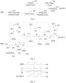
Fig. 1 is a functional block diagram of a phase tracking pulse generation circuit according to an embodiment of this application. -
Fig. 2 is a schematic structural diagram of the phase tracking pulse generation circuit according to an embodiment of this application. -
Fig. 3 is a diagram of voltage waveforms at points DRV, A, B, C, and OUTPUT inFig. 2 . - Description of reference numerals:
No. Name No. Name 100 Constant current circuit DRV DRV Drive pulse 200 Charge and discharge circuit Q1~Q2 First transistor to second transistor 300 Peak voltage circuit D1~D3 First diode to third diode 400 Comparison circuit R1~R7 First resistor to seventh resistor 500 Pulse rising edge extraction circuit C1~C3 First capacitor to third capacitor 600 Switch circuit GND Grounded 310 Peak sampling unit VCC Power supply 320 Voltage regulation unit OUTPUT Output pulse - The realization, functional characteristics, and advantages of the purpose of this application will be further described in conjunction with the embodiments and with reference to the accompanying drawings.
- The technical solutions in the embodiments of this application will be described clearly and completely in conjunction with the drawings in the embodiments of this application. Obviously, the described embodiments are only a part of the embodiments of this application, but not all the embodiments. Based on the embodiments in this application, all other embodiments obtained by those of ordinary skill in the art without creative work shall fall within the protection scope of this application.
- It should be noted that if there is a directional indication (such as up, down, left, right, front, back...) in the embodiment of this application, the directional indication is only used to explain the relative positional relationship, movement conditions, etc. among the components in a specific posture (as shown in the drawings), if the specific posture changes, the directional indicator also changes accordingly.
- In addition, if there are descriptions related to "first", "second", etc. in the embodiments of this application, the descriptions of "first", "second", etc. are for descriptive purposes only, and cannot be understood as indicating or implying their relative importance or implicitly indicating the number of indicated technical features. Thus, the features defined as "first" and "second" may include at least one of the features either explicitly or implicitly. In addition, the technical solutions between the various embodiments can be combined with each other, but they must be based on the ability of those skilled in the art to realize. When the combination of technical solutions conflicts with each other or cannot be realized, it should be considered that the combination of such technical solutions does not exist, nor within the scope of protection required by this application.
- This application provides a phase tracking pulse generation circuit.
- Referring to
Fig. 1 , in an embodiment, the circuit includes a constantcurrent circuit 100, apeak voltage circuit 300, a pulse risingedge extraction circuit 500, aswitch circuit 600, a charge anddischarge circuit 200, and acomparison circuit 400. The pulse risingedge extraction circuit 500 is configured to receive a drive pulse DRV output by a first power supply. Thecomparison circuit 400 is configured to output a phase tracking pulse OUTPUT to a second power supply. The constantcurrent circuit 100 is connected to thepeak voltage circuit 300 and the charge anddischarge circuit 200 respectively. The pulse risingedge extraction circuit 500 is connected to theswitch circuit 600. Theswitch circuit 600 is connected to the charge anddischarge circuit 200 and thecomparison circuit 400 respectively. The charge anddischarge circuit 200 is connected to thecomparison circuit 400. The constantcurrent circuit 100 is configured to generate a constant current, and charge the charge anddischarge circuit 200. The pulse risingedge extraction circuit 500 is configured to extract the drive pulse DRV of the first power supply, and control on and off of theswitch circuit 600 according to the drive pulse DRV. Theswitch circuit 600 is configured to control the charge anddischarge circuit 200 to discharge when the switch circuit is turned on. The charge anddischarge circuit 200 is configured to provide a first voltage to thecomparison circuit 400 during charge or discharge. Thepeak voltage circuit 300 is configured to extract a peak voltage of the charge anddischarge circuit 200, adjust the peak voltage to obtain a second voltage, and output the second voltage to thecomparison circuit 400. Thecomparison circuit 400 is configured to compare the first voltage with the second voltage and output the phase tracking pulse. - It should be noted that when the two power supplies work at the same time, if the two power supplies work in staggered phases, the peak current during operation is small, and the interference caused is small, which is beneficial to the stable operation of the power supply system. At the same time, because the two power supplies work in staggered phases, the instantaneous peak power is small and the interference to other devices is small. Therefore, in this embodiment, a synchronization signal is needed to coordinate the operation of the two power supplies. In this embodiment, a rising edge of a drive pulse of a power supply is taken as a reference, and a constant current circuit charges a capacitor in a charge and discharge circuit with constant current. When the rising edge of the reference drive pulse comes, the capacitor is discharged. A peak voltage on the capacitor is taken out and divided to be compared with a voltage on the charge and discharge circuit. When the voltage on the capacitor is equal to the divided value of the peak voltage, the output of the comparison circuit turns high. The output of the comparator is the phase tracking pulse.
- In this embodiment, by generating a pulse signal with a fixed phase relationship with the power supply drive pulse, the rising edge of the pulse signal may be configured to synchronize another power supply, thereby reducing the peak power of the power supplies, reducing interference generated by the power supplies, and improving the reliability of the power supplies themselves. This application is suitable for staggered-phase working of two power supplies.
- Referring to
Fig. 2 , in an embodiment, thepeak voltage circuit 300 includes apeak sampling unit 310 and avoltage regulation unit 320. Thepeak sampling unit 310 is connected to the constantcurrent circuit 100, the charge anddischarge circuit 200, and thevoltage regulation unit 320 respectively. Thevoltage regulation unit 320 is connected to thecomparison circuit 400. - It should be noted that after being taken out from the charge and
discharge circuit 200 by thepeak sampling unit 310, the peak voltage is divided by thevoltage regulation unit 320. After the voltage division, the voltage at point C is related to the resistance of thevoltage regulation unit 320, and the voltage magnitude of the point C determines the phase relationship between the output pulse signal and the input drive pulse. - In order to extract the peak voltage of the charge and
discharge circuit 200, thepeak sampling unit 310 includes a first comparator U1, a first resistor R1, a first diode D1 and a first capacitor C1. A first voltage input terminal of the first comparator U1 is connected to the constantcurrent circuit 100 and the charge anddischarge circuit 200 respectively. A second voltage input terminal of the first comparator U1 is connected to a first terminal of the first capacitor C1 and thevoltage regulation unit 320 respectively. An output terminal of the first comparator U1 is connected to a first terminal of the first resistor R1 and an anode of the first diode D1 respectively. A power input terminal of the first comparator U1 is connected to a power supply VCC. A ground terminal of the first comparator U1 is grounded. A second terminal of the first resistor R1 is connected to the power supply VCC. A cathode of the first diode D1 is connected to the second voltage input terminal of the first comparator U1, the first terminal of the first capacitor C1 and thevoltage regulation unit 320 respectively. A second terminal of the first capacitor C1 is grounded. - It should be understood that the first comparator U1 may be a general low-cost comparator, such as LM393, of course, it may also be of other types, which is not limited in this embodiment.
- Further, in order to determine the phase relationship between the output pulse signal and the input drive pulse, the
voltage regulation unit 320 includes a second resistor R2 and a third resistor R3. A first terminal of the second resistor R2 is connected to the cathode of the first diode D1 and the first terminal of the first capacitor C1 respectively. A second terminal of the second resistor R2 is connected to thecomparison circuit 400, and the second terminal of the second resistor R2 is further grounded through the third resistor R3. - It should be noted that the second resistor R2 and the third resistor R3 are both voltage divider resistors, which are configured to divide the peak voltage extracted from the
peak sampling unit 310. When the resistance values of the second resistor R2 and the third resistor R3 are equal, the output pulse phase forms a 90-degree phase of the pulse delayed drive pulse. - In addition, the first resistor R1 is a pull-up resistor. In order to improve the peak sampling accuracy and response speed, and to reduce the sampling error, the resistance of the first resistor R1 should be less than 100 times the sum of the resistance of the second resistor R2 and the third resistor R3.
- The constant
current circuit 100 includes a first triode Q1, a fourth resistor R4, a fifth resistor R5, and a second diode D2. A base of the first triode Q1 is grounded through the fourth resistor R4, and the base of the first triode Q1 is further connected to an anode of the second diode D2. An emitter of the first triode Q1 is connected to a first terminal of the fifth resistor R5. A collector of the first triode Q1 is connected to the first voltage input terminal of the first comparator U1 and the charge anddischarge circuit 200 respectively. A cathode of the second diode D2 is connected to the power supply VCC. A second terminal of the fifth resistor R5 is connected to the power supply VCC. - It is understandable that the power supply VCC provides a VCC voltage to power the entire phase tracking pulse generation circuit.
- The second diode D2 is a Zener diode for generating a stable voltage value.
- The constant
current circuit 100 is configured to generate a constant current, and the constant current value is: (VD2-VQ1eb)/R5, where VD2 is voltage stabilization value of Zener diode D2, and VQleb is voltage value between e-b poles of the first transistor Q1; the constant current generated by the constantcurrent circuit 100 is configured to linearly charge the charge anddischarge circuit 200. - Optionally, the charge and
discharge circuit 200 includes a second capacitor C2. A first terminal of the second capacitor C2 is connected to thecomparison circuit 400, the collector of the first triode Q1, theswitch circuit 600 and the first voltage input terminal of the first comparator U1 respectively. A second terminal of the second capacitor C2 is grounded. - It should be understood that the
comparison circuit 400 obtains different voltage values by charging and discharging the second capacitor C2, so as to output a phase tracking pulse after comparison. - The pulse rising
edge extraction circuit 500 includes a third capacitor C3, a third diode D3, and a sixth resistor R6. A first terminal of the third capacitor C3 is configured to receive the drive pulse DRV output by the first power supply. A second terminal of the third capacitor C3 is grounded through the third diode D3. The second terminal of the third capacitor C3 is further grounded through the sixth resistor R6. The second terminal of the third capacitor C3 is further connected to theswitch circuit 600. - Further, the
switch circuit 600 includes a second triode Q2. A gate of the second triode Q2 is connected to the second terminal of the third capacitor C3. A drain of the second triode Q2 is connected to thecomparison circuit 400 and the first terminal of the second capacitor C2 respectively. A source of the second triode Q2 is grounded. - It should be noted that the second triode Q2 is a Metal-Oxide-Semiconductor Field-Effect Transistor (MOSFET), which functions as a controlled switch.
- In implementation, the pulse rising
edge extraction circuit 500 is configured to extract the main power supply or the first power drive pulse DRV rising edge narrow pulse, and control the second triode Q2 to turn on or off. When the pulse risingedge extraction circuit 500 extracts the drive pulse rising edge narrow pulse, the second triode Q2 is turned on, otherwise, the second triode Q2 is turned off. - The comparison circuit includes a second comparator U2 and a seventh resistor R7. A first voltage input terminal of the second comparator U2 is connected to the first terminal of the second capacitor C2. A second voltage input terminal of the second comparator U2 is connected to a first terminal of the third resistor R3. A power input terminal of the second comparator U2 is connected to the power supply VCC. A ground terminal of the second comparator U2 is grounded. An output terminal of the second comparator U2 is connected to a first terminal of the seventh resistor R7 and the second power supply respectively. A second terminal of the seventh resistor R7 is connected to the power supply VCC.
- It should be understood that the second comparator U2 may be a general low-cost comparator, such as LM393, of course, it may also be of other types, which is not limited in this embodiment.
- In the implementation, the seventh resistor R7 is a pull-up resistor, which cooperates with the second comparator U2 to output the required waveform. The second comparator U2 is configured to compare the divided voltage of the peak voltage with the voltage of the second capacitor C2, that is, the voltages at point C and point B. When VC>VB, the comparator U2 outputs a high level through the pull-up resistor R7. When VC<VB, the comparator U2 outputs a low level, and the voltage waveform diagrams at points DRV, A, B, C, and OUTPUT are shown in
Fig. 3 . - In this embodiment, the accuracy of voltage peak sampling is improved by setting the resistance of the pull-up resistor in the peak sampling unit. By adjusting the resistance of the resistor in the voltage regulation unit, a pulse signal with a fixed phase relationship with the power supply drive pulse may be generated, and the rising edge of the pulse signal may be configured to synchronize another power supply, thereby reducing the peak power of the power supplies, reducing interference generated by the power supplies, and improving the reliability of the power supplies themselves. This application is suitable for staggered-phase working of two power supplies.
- This application further provides a power supply device. The power supply device includes the phase tracking pulse generation circuit as described above. For the circuit structure of the phase tracking pulse generation circuit of the power supply device, refer to the above-mentioned embodiments, which will not be repeated here. It is understood that since the power supply device of this embodiment adopts the technical solution of the above-mentioned phase tracking pulse generation circuit, the power supply device has all the above-mentioned beneficial effects.
- The above are only optional embodiments of this application and do not limit the patent scope of this application. Any equivalent structure or equivalent process transformation made by the description and drawings of this application, or directly or indirectly used in other related technical fields are similarly included in the patent protection scope of this application.
Claims (20)
- A phase tracking pulse generation circuit, comprising a constant current circuit, a peak voltage circuit, a pulse rising edge extraction circuit, a switch circuit, a charge and discharge circuit, and a comparison circuit; wherein the pulse rising edge extraction circuit is configured to receive a drive pulse output by a first power supply, the comparison circuit is configured to output a phase tracking pulse to a second power supply, the constant current circuit is connected to the peak voltage circuit and the charge and discharge circuit respectively, the pulse rising edge extraction circuit is connected to the switch circuit, the switch circuit is connected to the charge and discharge circuit and the comparison circuit respectively, and the charge and discharge circuit is connected to the comparison circuit; wherein,the constant current circuit is configured to generate a constant current, and charge the charge and discharge circuit;the pulse rising edge extraction circuit is configured to extract the drive pulse of the first power supply, and control on and off of the switch circuit according to the drive pulse;the switch circuit is configured to control the charge and discharge circuit to discharge when the switch circuit is turned on;the charge and discharge circuit is configured to provide a first voltage to the comparison circuit during charge or discharge;the peak voltage circuit is configured to extract a peak voltage of the charge and discharge circuit, adjust the peak voltage to obtain a second voltage, and output the second voltage to the comparison circuit; andthe comparison circuit is configured to compare the first voltage with the second voltage and output the phase tracking pulse.
- The phase tracking pulse generation circuit of claim 1, wherein the peak voltage circuit comprises a peak sampling unit and a voltage regulation unit; the peak sampling unit is connected to the constant current circuit, the charge and discharge circuit, and the voltage regulation unit respectively, and the voltage regulation unit is connected to the comparison circuit.
- The phase tracking pulse generation circuit of claim 2, wherein the peak sampling unit comprises a first comparator, a first resistor, a first diode and a first capacitor; wherein,a first voltage input terminal of the first comparator is connected to the constant current circuit and the charge and discharge circuit respectively, a second voltage input terminal of the first comparator is connected to a first terminal of the first capacitor and the voltage regulation unit respectively, an output terminal of the first comparator is connected to a first terminal of the first resistor and an anode of the first diode respectively, a power input terminal of the first comparator is connected to a power supply, and a ground terminal of the first comparator is grounded;a second terminal of the first resistor is connected to the power supply;a cathode of the first diode is connected to the second voltage input terminal of the first comparator, the first terminal of the first capacitor and the voltage regulation unit respectively; anda second terminal of the first capacitor is grounded.
- The phase tracking pulse generation circuit of claim 3, wherein the voltage regulation unit comprises a second resistor and a third resistor; a first terminal of the second resistor is connected to the cathode of the first diode and the first terminal of the first capacitor respectively, a second terminal of the second resistor is connected to the comparison circuit, and the second terminal of the second resistor is further grounded through the third resistor.
- The phase tracking pulse generation circuit of claim 4, wherein the constant current circuit comprises a first triode, a fourth resistor, a fifth resistor, and a second diode; wherein,a base of the first triode is grounded through the fourth resistor, the base of the first triode is further connected to an anode of the second diode, and an emitter of the first triode is connected to a first terminal of the fifth resistor, and a collector of the first triode is connected to the first voltage input terminal of the first comparator and the charge and discharge circuit respectively;a cathode of the second diode is connected to the power supply; anda second terminal of the fifth resistor is connected to the power supply.
- The phase tracking pulse generation circuit of claim 5, wherein the second diode is a Zener diode.
- The phase tracking pulse generation circuit of claim 5, wherein the charge and discharge circuit comprises a second capacitor; a first terminal of the second capacitor is connected to the comparison circuit, the collector of the first triode, the switch circuit and the first voltage input terminal of the first comparator respectively, and a second terminal of the second capacitor is grounded.
- The phase tracking pulse generation circuit of claim 7, wherein the pulse rising edge extraction circuit comprises a third capacitor, a third diode, and a sixth resistor; a first terminal of the third capacitor is configured to receive the drive pulse output by the first power supply, a second terminal of the third capacitor is grounded through the third diode, the second terminal of the third capacitor is further grounded through the sixth resistor, and the second terminal of the third capacitor is further connected to the switch circuit.
- The phase tracking pulse generation circuit of claim 8, wherein the switch circuit comprises a second triode; a gate of the second triode is connected to the second terminal of the third capacitor, a drain of the second triode is connected to the comparison circuit and the first terminal of the second capacitor respectively, and a source of the second triode is grounded.
- The phase tracking pulse generation circuit of claim 9, wherein the comparison circuit comprises a second comparator and a seventh resistor; wherein,a first voltage input terminal of the second comparator is connected to the first terminal of the second capacitor, a second voltage input terminal of the second comparator is connected to a first terminal of the third resistor, a power input terminal of the second comparator is connected to the power supply, a ground terminal of the second comparator is grounded, and an output terminal of the second comparator is connected to a first terminal of the seventh resistor and the second power supply respectively; anda second terminal of the seventh resistor is connected to the power supply.
- A power supply device, comprising a phase tracking pulse generation circuit, wherein the phase tracking pulse generation circuit comprises a constant current circuit, a peak voltage circuit, a pulse rising edge extraction circuit, a switch circuit, a charge and discharge circuit, and a comparison circuit; the pulse rising edge extraction circuit is configured to receive a drive pulse output by a first power supply, the comparison circuit is configured to output a phase tracking pulse to a second power supply, the constant current circuit is connected to the peak voltage circuit and the charge and discharge circuit respectively, the pulse rising edge extraction circuit is connected to the switch circuit, the switch circuit is connected to the charge and discharge circuit and the comparison circuit respectively, and the charge and discharge circuit is connected to the comparison circuit; wherein,the constant current circuit is configured to generate a constant current, and charge the charge and discharge circuit;the pulse rising edge extraction circuit is configured to extract the drive pulse of the first power supply, and control on and off of the switch circuit according to the drive pulse;the switch circuit is configured to control the charge and discharge circuit to discharge when the switch circuit is turned on;the charge and discharge circuit is configured to provide a first voltage to the comparison circuit during charge or discharge;the peak voltage circuit is configured to extract a peak voltage of the charge and discharge circuit, adjust the peak voltage to obtain a second voltage, and output the second voltage to the comparison circuit; andthe comparison circuit is configured to compare the first voltage with the second voltage and output the phase tracking pulse.
- The power supply device of claim 11, wherein the peak voltage circuit comprises a peak sampling unit and a voltage regulation unit; the peak sampling unit is connected to the constant current circuit, the charge and discharge circuit, and the voltage regulation unit respectively, and the voltage regulation unit is connected to the comparison circuit.
- The power supply device of claim 12, wherein the peak sampling unit comprises a first comparator, a first resistor, a first diode and a first capacitor; wherein,a first voltage input terminal of the first comparator is connected to the constant current circuit and the charge and discharge circuit respectively, a second voltage input terminal of the first comparator is connected to a first terminal of the first capacitor and the voltage regulation unit respectively, an output terminal of the first comparator is connected to a first terminal of the first resistor and an anode of the first diode respectively, a power input terminal of the first comparator is connected to a power supply, and a ground terminal of the first comparator is grounded;a second terminal of the first resistor is connected to the power supply;a cathode of the first diode is connected to the second voltage input terminal of the first comparator, the first terminal of the first capacitor and the voltage regulation unit respectively; anda second terminal of the first capacitor is grounded.
- The power supply device of claim 13, wherein the voltage regulation unit comprises a second resistor and a third resistor; a first terminal of the second resistor is connected to the cathode of the first diode and the first terminal of the first capacitor respectively, a second terminal of the second resistor is connected to the comparison circuit, and the second terminal of the second resistor is further grounded through the third resistor.
- The power supply device of claim 14, wherein the constant current circuit comprises a first triode, a fourth resistor, a fifth resistor, and a second diode; wherein,a base of the first triode is grounded through the fourth resistor, the base of the first triode is further connected to an anode of the second diode, and an emitter of the first triode is connected to a first terminal of the fifth resistor, and a collector of the first triode is connected to the first voltage input terminal of the first comparator and the charge and discharge circuit respectively;a cathode of the second diode is connected to the power supply; anda second terminal of the fifth resistor is connected to the power supply.
- The power supply device of claim 15, wherein the second diode is a Zener diode.
- The power supply device of claim 15, wherein the charge and discharge circuit comprises a second capacitor; a first terminal of the second capacitor is connected to the comparison circuit, the collector of the first triode, the switch circuit and the first voltage input terminal of the first comparator respectively, and a second terminal of the second capacitor is grounded.
- The power supply device of claim 17, wherein the pulse rising edge extraction circuit comprises a third capacitor, a third diode, and a sixth resistor; a first terminal of the third capacitor is configured to receive the drive pulse output by the first power supply, a second terminal of the third capacitor is grounded through the third diode, the second terminal of the third capacitor is further grounded through the sixth resistor, and the second terminal of the third capacitor is further connected to the switch circuit.
- The power supply device of claim 18, wherein the switch circuit comprises a second triode; a gate of the second triode is connected to the second terminal of the third capacitor, a drain of the second triode is connected to the comparison circuit and the first terminal of the second capacitor respectively, and a source of the second triode is grounded.
- The power supply device of claim 19, wherein the comparison circuit comprises a second comparator and a seventh resistor; wherein,a first voltage input terminal of the second comparator is connected to the first terminal of the second capacitor, a second voltage input terminal of the second comparator is connected to a first terminal of the third resistor, a power input terminal of the second comparator is connected to the power supply, a ground terminal of the second comparator is grounded, and an output terminal of the second comparator is connected to a first terminal of the seventh resistor and the second power supply respectively; anda second terminal of the seventh resistor is connected to the power supply.
Applications Claiming Priority (2)
| Application Number | Priority Date | Filing Date | Title |
|---|---|---|---|
| CN201920362051.7U CN209462353U (en) | 2019-03-20 | 2019-03-20 | Phase afterpulsing generation circuit and power supply device |
| PCT/CN2020/079314 WO2020187163A1 (en) | 2019-03-20 | 2020-03-13 | Phase-tracked pulse generation circuit and power supply device |
Publications (3)
| Publication Number | Publication Date |
|---|---|
| EP3944498A1 true EP3944498A1 (en) | 2022-01-26 |
| EP3944498A4 EP3944498A4 (en) | 2022-05-04 |
| EP3944498B1 EP3944498B1 (en) | 2025-12-10 |
Family
ID=68047417
Family Applications (1)
| Application Number | Title | Priority Date | Filing Date |
|---|---|---|---|
| EP20772727.2A Active EP3944498B1 (en) | 2019-03-20 | 2020-03-13 | Phase-tracked pulse generation circuit and power supply device |
Country Status (4)
| Country | Link |
|---|---|
| US (1) | US11444604B2 (en) |
| EP (1) | EP3944498B1 (en) |
| CN (1) | CN209462353U (en) |
| WO (1) | WO2020187163A1 (en) |
Families Citing this family (4)
| Publication number | Priority date | Publication date | Assignee | Title |
|---|---|---|---|---|
| CN209462353U (en) * | 2019-03-20 | 2019-10-01 | 深圳Tcl新技术有限公司 | Phase afterpulsing generation circuit and power supply device |
| CN111708000A (en) * | 2020-06-06 | 2020-09-25 | 深圳市欢创科技有限公司 | A signal shaping circuit, lidar and mobile robot |
| CN116232287B (en) * | 2023-01-16 | 2025-11-25 | 苏州国芯科技股份有限公司 | A synchronization pulse generation circuit and electronic control unit |
| CN119051641B (en) * | 2024-08-15 | 2025-05-13 | 宁波兴为汽车电子有限公司 | NMOS tube high-side driving circuit, system and device |
Family Cites Families (11)
| Publication number | Priority date | Publication date | Assignee | Title |
|---|---|---|---|---|
| US20090225020A1 (en) * | 2008-03-07 | 2009-09-10 | O2Micro, Inc. | Backlight controller for driving light sources |
| US8138734B2 (en) * | 2009-04-06 | 2012-03-20 | Monolithic Power Systems, Inc. | Accurate current limit for peak current mode DC-DC converter |
| JP5788748B2 (en) * | 2011-09-13 | 2015-10-07 | リコー電子デバイス株式会社 | DC / DC converter control circuit and DC-DC converter |
| CN103116062B (en) | 2013-03-11 | 2015-07-08 | 矽力杰半导体技术(杭州)有限公司 | Circuit and method for detecting voltage peak |
| TWI493848B (en) * | 2013-05-20 | 2015-07-21 | Richtek Technology Corp | Power converter and power factor correction device |
| US9350281B2 (en) * | 2014-05-09 | 2016-05-24 | Alonso Rodiguez | Circuit and method for frequency synthesis for signal detection in automatic voltage regulation for synchronous generators |
| US9717123B1 (en) * | 2016-10-17 | 2017-07-25 | Integrated Silicon Solution, Inc. | Audible noise reduction method for multiple LED channel systems |
| CN109302066B (en) * | 2017-07-25 | 2020-06-26 | 上海三思电子工程有限公司 | Sampling circuit of primary inductance peak current in switching power supply and switching power supply |
| CN107942127B (en) | 2017-11-17 | 2021-01-01 | 亿嘉和科技股份有限公司 | Peak detection circuit |
| US10630275B2 (en) * | 2018-02-26 | 2020-04-21 | Nxp B.V. | Constant-on-time pulse generator circuit for a DC-DC converter |
| CN209462353U (en) | 2019-03-20 | 2019-10-01 | 深圳Tcl新技术有限公司 | Phase afterpulsing generation circuit and power supply device |
-
2019
- 2019-03-20 CN CN201920362051.7U patent/CN209462353U/en not_active Expired - Fee Related
-
2020
- 2020-03-13 WO PCT/CN2020/079314 patent/WO2020187163A1/en not_active Ceased
- 2020-03-13 US US17/266,681 patent/US11444604B2/en active Active
- 2020-03-13 EP EP20772727.2A patent/EP3944498B1/en active Active
Also Published As
| Publication number | Publication date |
|---|---|
| EP3944498B1 (en) | 2025-12-10 |
| CN209462353U (en) | 2019-10-01 |
| US20210305970A1 (en) | 2021-09-30 |
| EP3944498A4 (en) | 2022-05-04 |
| WO2020187163A1 (en) | 2020-09-24 |
| US11444604B2 (en) | 2022-09-13 |
Similar Documents
| Publication | Publication Date | Title |
|---|---|---|
| US11444604B2 (en) | Phase tracking pulse generation circuit and power supply device | |
| CN110098735B (en) | A kind of control method of switch circuit | |
| US20130033236A1 (en) | Systems and methods for discharging an ac input capacitor with automatic detection | |
| CN103166173A (en) | overvoltage protection circuit | |
| US10171035B2 (en) | Power factor correction circuit and multiplier | |
| CN114337261B (en) | A control system for synchronous rectifiers in a four-switch buck-boost converter | |
| CN114665854A (en) | Reset circuit and charging system | |
| US20180191249A1 (en) | Switching regulator | |
| CN111462708A (en) | Voltage conversion circuit, voltage conversion method and display device | |
| CN104362846B (en) | A kind of controllable multi-channel output DC-DC inverter of electrifying timing sequence | |
| US20160352312A1 (en) | Level conversion circuit and apparatus | |
| CN103929155B (en) | Pulse width widening circuit | |
| CN115085700A (en) | Solid-state pulse source output waveform delay control device and method | |
| CN221151333U (en) | Substrate selection circuit and charging chip | |
| CN210351116U (en) | Time delay control circuit | |
| CN116646896A (en) | Overvoltage protection circuit and electronic product | |
| CN210429272U (en) | VCOM voltage regulating circuit of LCD display screen | |
| CN108169596B (en) | Calibration system of input current channel of photovoltaic inverter and method for calibrating by using calibration system | |
| CN112542818B (en) | Input undervoltage protection circuit and power panel comprising same | |
| CN223986948U (en) | Power supply circuit and power supply system | |
| CN219420550U (en) | Power supply voltage regulating circuit and power supply system | |
| CN221177679U (en) | New thyristor digital trigger circuit and pulse generator | |
| CN222127906U (en) | Power supply drive control circuit and equipment | |
| US4163179A (en) | Circuit for providing saw-tooth current in a coil | |
| CN218482777U (en) | External simulation soft start circuit |
Legal Events
| Date | Code | Title | Description |
|---|---|---|---|
| STAA | Information on the status of an ep patent application or granted ep patent |
Free format text: STATUS: THE INTERNATIONAL PUBLICATION HAS BEEN MADE |
|
| PUAI | Public reference made under article 153(3) epc to a published international application that has entered the european phase |
Free format text: ORIGINAL CODE: 0009012 |
|
| STAA | Information on the status of an ep patent application or granted ep patent |
Free format text: STATUS: REQUEST FOR EXAMINATION WAS MADE |
|
| 17P | Request for examination filed |
Effective date: 20210205 |
|
| AK | Designated contracting states |
Kind code of ref document: A1 Designated state(s): AL AT BE BG CH CY CZ DE DK EE ES FI FR GB GR HR HU IE IS IT LI LT LU LV MC MK MT NL NO PL PT RO RS SE SI SK SM TR |
|
| A4 | Supplementary search report drawn up and despatched |
Effective date: 20220404 |
|
| RIC1 | Information provided on ipc code assigned before grant |
Ipc: H03K 3/013 20060101AFI20220329BHEP |
|
| DAV | Request for validation of the european patent (deleted) | ||
| DAX | Request for extension of the european patent (deleted) | ||
| GRAP | Despatch of communication of intention to grant a patent |
Free format text: ORIGINAL CODE: EPIDOSNIGR1 |
|
| STAA | Information on the status of an ep patent application or granted ep patent |
Free format text: STATUS: GRANT OF PATENT IS INTENDED |
|
| INTG | Intention to grant announced |
Effective date: 20250715 |
|
| RAP3 | Party data changed (applicant data changed or rights of an application transferred) |
Owner name: SHENZHEN TCL NEW TECHNOLOGY CO., LTD. |
|
| P01 | Opt-out of the competence of the unified patent court (upc) registered |
Free format text: CASE NUMBER: UPC_APP_3582_3944498/2025 Effective date: 20250818 |
|
| GRAS | Grant fee paid |
Free format text: ORIGINAL CODE: EPIDOSNIGR3 |
|
| GRAA | (expected) grant |
Free format text: ORIGINAL CODE: 0009210 |
|
| STAA | Information on the status of an ep patent application or granted ep patent |
Free format text: STATUS: THE PATENT HAS BEEN GRANTED |
|
| AK | Designated contracting states |
Kind code of ref document: B1 Designated state(s): AL AT BE BG CH CY CZ DE DK EE ES FI FR GB GR HR HU IE IS IT LI LT LU LV MC MK MT NL NO PL PT RO RS SE SI SK SM TR |
|
| REG | Reference to a national code |
Ref country code: CH Ref legal event code: F10 Free format text: ST27 STATUS EVENT CODE: U-0-0-F10-F00 (AS PROVIDED BY THE NATIONAL OFFICE) Effective date: 20251210 Ref country code: GB Ref legal event code: FG4D |
|
| REG | Reference to a national code |
Ref country code: DE Ref legal event code: R096 Ref document number: 602020063698 Country of ref document: DE |
|
| REG | Reference to a national code |
Ref country code: IE Ref legal event code: FG4D |
|
| PG25 | Lapsed in a contracting state [announced via postgrant information from national office to epo] |
Ref country code: ES Free format text: LAPSE BECAUSE OF FAILURE TO SUBMIT A TRANSLATION OF THE DESCRIPTION OR TO PAY THE FEE WITHIN THE PRESCRIBED TIME-LIMIT Effective date: 20251210 |
|
| REG | Reference to a national code |
Ref country code: LT Ref legal event code: MG9D |
|
| PG25 | Lapsed in a contracting state [announced via postgrant information from national office to epo] |
Ref country code: NO Free format text: LAPSE BECAUSE OF FAILURE TO SUBMIT A TRANSLATION OF THE DESCRIPTION OR TO PAY THE FEE WITHIN THE PRESCRIBED TIME-LIMIT Effective date: 20260310 |
|
| PGFP | Annual fee paid to national office [announced via postgrant information from national office to epo] |
Ref country code: DE Payment date: 20260319 Year of fee payment: 7 |
|
| PG25 | Lapsed in a contracting state [announced via postgrant information from national office to epo] |
Ref country code: FI Free format text: LAPSE BECAUSE OF FAILURE TO SUBMIT A TRANSLATION OF THE DESCRIPTION OR TO PAY THE FEE WITHIN THE PRESCRIBED TIME-LIMIT Effective date: 20251210 Ref country code: HR Free format text: LAPSE BECAUSE OF FAILURE TO SUBMIT A TRANSLATION OF THE DESCRIPTION OR TO PAY THE FEE WITHIN THE PRESCRIBED TIME-LIMIT Effective date: 20251210 |
|
| REG | Reference to a national code |
Ref country code: NL Ref legal event code: MP Effective date: 20251210 |
|
| PG25 | Lapsed in a contracting state [announced via postgrant information from national office to epo] |
Ref country code: RS Free format text: LAPSE BECAUSE OF FAILURE TO SUBMIT A TRANSLATION OF THE DESCRIPTION OR TO PAY THE FEE WITHIN THE PRESCRIBED TIME-LIMIT Effective date: 20260310 |
|
| PG25 | Lapsed in a contracting state [announced via postgrant information from national office to epo] |
Ref country code: LV Free format text: LAPSE BECAUSE OF FAILURE TO SUBMIT A TRANSLATION OF THE DESCRIPTION OR TO PAY THE FEE WITHIN THE PRESCRIBED TIME-LIMIT Effective date: 20251210 |
|
| PG25 | Lapsed in a contracting state [announced via postgrant information from national office to epo] |
Ref country code: BG Free format text: LAPSE BECAUSE OF FAILURE TO SUBMIT A TRANSLATION OF THE DESCRIPTION OR TO PAY THE FEE WITHIN THE PRESCRIBED TIME-LIMIT Effective date: 20251210 |