EP3944344A1 - Light emitting element and method of manufacturing light emitting element - Google Patents
Light emitting element and method of manufacturing light emitting element Download PDFInfo
- Publication number
- EP3944344A1 EP3944344A1 EP21183868.5A EP21183868A EP3944344A1 EP 3944344 A1 EP3944344 A1 EP 3944344A1 EP 21183868 A EP21183868 A EP 21183868A EP 3944344 A1 EP3944344 A1 EP 3944344A1
- Authority
- EP
- European Patent Office
- Prior art keywords
- layer
- region
- type semiconductor
- conductivity type
- semiconductor layer
- Prior art date
- Legal status (The legal status is an assumption and is not a legal conclusion. Google has not performed a legal analysis and makes no representation as to the accuracy of the status listed.)
- Granted
Links
Images








Classifications
-
- H—ELECTRICITY
- H10—SEMICONDUCTOR DEVICES; ELECTRIC SOLID-STATE DEVICES NOT OTHERWISE PROVIDED FOR
- H10H—INORGANIC LIGHT-EMITTING SEMICONDUCTOR DEVICES HAVING POTENTIAL BARRIERS
- H10H20/00—Individual inorganic light-emitting semiconductor devices having potential barriers, e.g. light-emitting diodes [LED]
- H10H20/80—Constructional details
- H10H20/81—Bodies
- H10H20/819—Bodies characterised by their shape, e.g. curved or truncated substrates
-
- H—ELECTRICITY
- H10—SEMICONDUCTOR DEVICES; ELECTRIC SOLID-STATE DEVICES NOT OTHERWISE PROVIDED FOR
- H10H—INORGANIC LIGHT-EMITTING SEMICONDUCTOR DEVICES HAVING POTENTIAL BARRIERS
- H10H20/00—Individual inorganic light-emitting semiconductor devices having potential barriers, e.g. light-emitting diodes [LED]
- H10H20/01—Manufacture or treatment
- H10H20/011—Manufacture or treatment of bodies, e.g. forming semiconductor layers
- H10H20/013—Manufacture or treatment of bodies, e.g. forming semiconductor layers having light-emitting regions comprising only Group III-V materials
-
- H—ELECTRICITY
- H10—SEMICONDUCTOR DEVICES; ELECTRIC SOLID-STATE DEVICES NOT OTHERWISE PROVIDED FOR
- H10H—INORGANIC LIGHT-EMITTING SEMICONDUCTOR DEVICES HAVING POTENTIAL BARRIERS
- H10H20/00—Individual inorganic light-emitting semiconductor devices having potential barriers, e.g. light-emitting diodes [LED]
- H10H20/80—Constructional details
- H10H20/81—Bodies
-
- H—ELECTRICITY
- H10—SEMICONDUCTOR DEVICES; ELECTRIC SOLID-STATE DEVICES NOT OTHERWISE PROVIDED FOR
- H10H—INORGANIC LIGHT-EMITTING SEMICONDUCTOR DEVICES HAVING POTENTIAL BARRIERS
- H10H20/00—Individual inorganic light-emitting semiconductor devices having potential barriers, e.g. light-emitting diodes [LED]
- H10H20/80—Constructional details
- H10H20/81—Bodies
- H10H20/819—Bodies characterised by their shape, e.g. curved or truncated substrates
- H10H20/82—Roughened surfaces, e.g. at the interface between epitaxial layers
-
- H—ELECTRICITY
- H10—SEMICONDUCTOR DEVICES; ELECTRIC SOLID-STATE DEVICES NOT OTHERWISE PROVIDED FOR
- H10H—INORGANIC LIGHT-EMITTING SEMICONDUCTOR DEVICES HAVING POTENTIAL BARRIERS
- H10H20/00—Individual inorganic light-emitting semiconductor devices having potential barriers, e.g. light-emitting diodes [LED]
- H10H20/80—Constructional details
- H10H20/81—Bodies
- H10H20/822—Materials of the light-emitting regions
- H10H20/824—Materials of the light-emitting regions comprising only Group III-V materials, e.g. GaP
- H10H20/825—Materials of the light-emitting regions comprising only Group III-V materials, e.g. GaP containing nitrogen, e.g. GaN
-
- H—ELECTRICITY
- H10—SEMICONDUCTOR DEVICES; ELECTRIC SOLID-STATE DEVICES NOT OTHERWISE PROVIDED FOR
- H10H—INORGANIC LIGHT-EMITTING SEMICONDUCTOR DEVICES HAVING POTENTIAL BARRIERS
- H10H20/00—Individual inorganic light-emitting semiconductor devices having potential barriers, e.g. light-emitting diodes [LED]
- H10H20/80—Constructional details
- H10H20/83—Electrodes
- H10H20/831—Electrodes characterised by their shape
- H10H20/8312—Electrodes characterised by their shape extending at least partially through the bodies
Definitions
- the semiconductor stack 20 has a first conductivity type semiconductor layer 10, a second conductivity type semiconductor layer 15, and an active layer 14.
- the active layer 14 is disposed between the first conductivity type semiconductor layer 10 and the second conductivity type semiconductor layer 15 and is an emission layer that emits light
- the peak wavelength of the light from the active layer 14 is no more than 400 nm, specifically 210 nm to 400 nm, more specifically 300 nm to 400 nm.
- the active layer 14 emits ultraviolet light Because the thickness of the active layer 14 is smaller than the thicknesses of the first conductivity type semiconductor layer 10 and the second conductivity type semiconductor layer 15, it is indicated by a line in FIG. 2 . Similarly, the active layer 14 is shown as a line in FIGS. 4 to 13 and FIGS. 15 to 19 .
- a plurality of second regions a2 are arranged in island shapes, and the second regions a2 are surrounded by the first region a1.
- the area of the first region a1 is larger than the sum of the areas of the second regions a2.
- the light emitting element 1 further has a first conductive member 40, a second conductive member 50, a third conductive member 60, a reflective electrode 30, a first pad electrode 71, a second pad electrode 72, and first to fourth insulating films 81 to 84.
- the surface of the second conductivity type semiconductor layer 15 also has a region in which the reflective electrode 30 is not disposed.
- the region is covered by a first insulating film 81.
- the first insulating film 81 also covers a portion of the reflective electrode 30.
- the first insulating film 81 is, for example, a silicon nitride film or silicon oxide film.
- the reflective electrode 30 has a surface exposed from the first insulating film 81 and the second insulating film 82.
- the reflective electrode 30 is in contact with the p-side conductive part 50a of the second conductive member 50.
- the second conductive member 50 is electrically connected via the p-side conductive part 50a and the reflective electrode 30 to the second conductivity type semiconductor layer 15 stacked in the first region a1.
- the third insulating film 83 is disposed between the first conductive member 40 and the second conductive member 50, and the first conductive member 40 and the second conductive member 50 are insulated and separated from one another by the third insulating film 83.
- the support substrate 100 is square shaped in a top view.
- a first pad electrode 71 and a second pad electrode 72 are arranged at diagonal positions on the support substrate 100.
- the semiconductor stack 20 in a top view is formed to have a substantially square shape without the two diagonal corners where the first pad electrode 71 and the second pad electrode 72 are arranged.
- the first conductive member 40 has a pad connection part 40b positioned under the first pad electrode 71.
- a third conductive member 60 is disposed on the pad connection part 40b.
- the third conductive member 60 can be formed, for example, by using the same materials and the same process as those for forming the second conductive member 50.
- the third conductive member 60 is formed as an island shape separated from the second conductive member 50.
- the first pad electrode 71 is disposed on the third conductive member 60.
- the first pad electrode 71 is electrically connected to the first conductive member 40 via the third conductive member 60.
- the first pad electrode 71 and the second pad electrode 72 for example, contains at least one metal selected from the group consisting of Ti, Pt, and Au.
- the first conductive member 40 is bonded to the support substrate 100 via the bonding layer 101.
- the bonding layer 101 is a metal layer that contains a soldering material such as Sn.
- the support substrate 100 for example, is a silicon substrate.
- the upper face and the lateral faces of the semiconductor stack 20 are covered by a fourth insulating film 84.
- the upper face of the semiconductor stack 20 includes the first face 12a of the second layer 12 in the first region a1, the third face 11 a of the first layer 11 in the second regions a2, and the fifth face 11 b of the first layer 11 in the peripheral portion.
- the fourth insulating film 84 is, for example, a silicon oxide film.
- the arithmetic mean height of the protrusions formed on the surface of the fourth insulating film 84 in the first region a1 is greater than the arithmetic mean height of the protrusions formed on the surface of the fourth insulating film 84 in the second regions a2.
- the arithmetic mean height of the protrusions formed on the surface of the fourth insulating film 84 in the first region a1 is greater than the arithmetic mean height of the protrusions formed on the surface of the fourth insulating film 84 in the peripheral portion of the first conductivity type semiconductor layer 10.
- the thickness of the first conductivity type semiconductor layer 10 in the first region a1 is smaller than the thickness of the first conductivity type semiconductor layer 10 in the second regions a2. Reducing the thickness of the first conductivity type semiconductor layer 10 in the first region a1, which greatly affects the light extraction efficiency, can reduce the light absorption in the first region a1, thereby increasing the light extraction efficiency.
- the first conductive member 40 is connected to the first conductivity type semiconductor layer 10, providing a current conducting part for the first conductivity type semiconductor layer 10.
- Forming not only a second layer 12, but also a first layer 11 that has a lower Al percentage composition than the second layer 12 in the second regions a2 can reduce the forward voltage (drive voltage) Vf as well as reducing the current concentration in the second regions a2 as compared to the case in which no first layer 11 is disposed in the second regions a2.
- making the thickness of the first conductivity type semiconductor layer 10 in the second regions a2 larger than the thickness of the first conductivity type semiconductor layer 10 in the first region a1 can reduce the resistance of the second regions a2 thereby lowering the Vf.
- the thickness of the second layer 12 having a higher Al percentage composition is thinner than the first layer 11. This can reduce the crack occurrence in the first conductivity type semiconductor layer 10.
- the Al percentage composition in the first conductivity type semiconductor layer 10 is preferably in a range of 1 % to 5%.
- the thickness of the second layer 12 in the second regions a2 is preferably smaller than the thickness of the first layer 11 in the second regions a2.
- the thickness of the second layer 12 in the second regions a2 is preferably no more than 80% of the thickness of the first layer 11 in the second regions a2. Making the thickness of the second layer 12 in the second regions a2 smaller than the thickness of the first layer 11 in the second regions a2 can reduce the crack occurrence in the first conductivity type semiconductor layer 10 while lowering the Vf in the second regions a2.
- the outer edge of the third face 11 a is positioned between the outer edge of the n-side conductive part 40a of the first conductive member 40 and the outer edge of the reflective electrode 30 in the top view. This can reduce the light absorption by the first layer 11 in the second regions a2 while hindering the current from concentrating in the second regions a2.
- an underlayer 201 including, for example, an undoped GaN layer is grown on a substrate 200.
- the thickness of the underlayer 201 is, for example, 6 ⁇ m to 8 ⁇ m.
- a semiconductor stack 20 is formed via the underlayer 201.
- the substrate 200 is a substrate for allowing nitride semiconductor layers to grow, for example, a sapphire substrate.
- a buffer layer formed of, for example, AlGaN or AlN, can be formed on the substrate 200 before allowing the underlayer 201 to grow.
- the semiconductor stack 20 includes a first conductivity type semiconductor layer 10, an active layer 14, and a second conductivity type semiconductor layer 15.
- the first conductivity type semiconductor layer 10 includes a first layer 11 and a second layer 12.
- the first layer 11, the second layer 12, the active layer 14, and the second conductivity type semiconductor layer 15 are successively epitaxially grown.
- MOCVD metal organic chemical vapor deposition
- the first conductivity type semiconductor layer 10 is a nitride semiconductor layer containing Al and Ga in which the first layer 11 has a lower Al percentage composition than the Al percentage composition of the second layer 12.
- the Al percentage composition of the first layer 11 is 3%
- the Al percentage composition of the second layer 12 is 5%.
- the first layer 11 In forming the semiconductor stack 20, it is preferable to form the first layer 11 to a thickness of, for example, 0.3 ⁇ m to 3 ⁇ m, more preferably 1 ⁇ m to 2.5 ⁇ m.
- the second layer 12 it is preferable to form the second layer 12 to a thickness of 0.3 ⁇ m to 1.5 ⁇ m, more preferably 0.5 ⁇ m to 1.2 ⁇ m.
- the thickness of the first layer 11 is set to be 2 ⁇ m
- the thickness of the second layer 12 is set to be 1 ⁇ m.
- the second conductivity type semiconductor layer 15 and the active layer 14 are partially removed.
- the second conductivity type semiconductor layer 15 and the active layer 14 are partially removed by RIE (reactive ion etching).
- RIE reactive ion etching
- the partial removal of the second conductivity type semiconductor layer 15 and the active layer 14 exposes portions of the second layer 12 of the first conductivity type semiconductor layer 10 from the second conductivity type semiconductor layer 15 and the active layer 14.
- the reflective electrode 30, the first insulating film 81, the second insulating film 82, the second conductive member 50, the third conductive member 60, the third insulating film 83, and the first conductive member 40 described earlier with reference to FIG. 2 are formed.
- the reflective electrode 30, the first insulating film 81, the second insulating film 82, the second conductive member 50, the third conductive member 60, the third insulating film 83, and the first conductive member 40 can be formed by, for example, sputtering, vapor deposition, or the like.
- the second conductive member 50 and the third conductive member 60 can be formed by the same process.
- the p-side conductive part 50a of the second conductive member 50 is in contact with the reflective electrode 30, and the n-side conductive part 40a of the first conductive member 40 is in contact with the second face 12b of the first conductivity type semiconductor layer 10.
- the first conductive member 40 is bonded to the support substrate 100 via a bonding layer 101.
- the structure in FIG. 5 is flipped upside down.
- the semiconductor stack 20 is bonded to the support substrate 100 while being held by the substrate 200.
- the first layer 11 in the second region a2 which includes the second face 12b to which the n-side conductive part 40a of the first conductive member 40 is connected, is covered by the mask 91 and not removed, allowing the second layer 12 and the first layer 11, which is thicker than the second layer 12 and has a lower Al percentage composition than the second layer 12, to remain.
- the etching rate for the first layer 11 in wet etching tends to be lower than the etching rate for the second layer 12. Reducing the etched amount of the third face 11 a in the second region a2 can moderate the reduction in the thickness of the first layer 11 in the second region a2. Because the Al percentage composition of the first layer 11 is lower than Al percentage composition of the second layer 12, moderating the reduction in the thickness of the first layer 11 in the second region a2 connected to the n-side conductive part 40a of the first conductive member 40 can, as described earlier, reduce the forward voltage (drive voltage) Vf.
- Such a roughening process allows the third face 11 a of the first layer 11 in the second region a2 to be unetched to remain flat as shown in FIG. 12 . This can make the first layer 11 in the second region a2 thicker, thereby reducing the Vf.
- FIG. 13 is a schematic cross-sectional view of a light emitting element according to a second embodiment of the present disclosure.
- the light emitting element according to the second embodiment has the same structure as the first embodiment shown in FIG. 2 except for the features described below. Only the differences from the first embodiment will basically be descried below.
- the first layer 11, the second layer 12, and the third layer 13 are stacked in the second region a2. Neither an active layer 14 nor second conductivity type semiconductor layer 15 is stacked in the second region a2.
- the face (sixth face) 13a of the third layer 13 on the support substrate 100 side in the second region a2 is exposed from the second conductivity type semiconductor layer 15 and the active layer 14.
- the n-side conductive part 40a of the first conductive member 40 is in contact with the sixth face 13a.
- a portion of the surface of the second conductivity type semiconductor layer 15 can be modified as shown in FIG. 16 .
- the portions of the surface of the second conductivity type semiconductor layer 15 marked with dot hatching are modified.
- a mask 500 is formed on a portion of the surface of the second conductivity type semiconductor layer 15, which will be positioned above the first region a1 of the first conductivity type semiconductor layer 10 described earlier. Then the surface of the second conductivity type semiconductor layer 15 exposed from the mask 500 is plasma treated in ambient air containing oxygen, for example.
- the modified surface of the second conductivity type semiconductor layer 15 has a higher resistance than the surface of the second conductivity type semiconductor layer 15 that is not modified.
- a low resistance portion (unmodified portion) 15a and a high resistance portion (modified portion) 15b having a higher resistance than that of the low resistance portion 15a are formed on the surface of the second conductivity type semiconductor layer 15.
- a reflective electrode 30 is formed on the surface of the second conductivity type semiconductor layer 15 so as to straddle the low resistance portion 15a and the high resistance portion 15b.
- the reflective electrode 30 is in contact with the entire low resistance portion 15a.
- the reflective electrode 30 is in contact with a portion of the high resistance portion 15b.
- the area of contact between the reflective electrode 30 and the low resistance portion 15a is larger than the area of contact between the reflective electrode 30 and the high resistance portion 15b.
- a first insulating film 81 is formed to cover the surfaces of the reflective electrode 30 and the second conductivity type semiconductor layer 15.
- a portion of the first insulating film 81, a portion of the second conductivity type semiconductor layer 15, and a portion of the active layer 14 are removed. This partially exposes the second layer 12 of the first conductivity type semiconductor layer 10 from the second conductivity type semiconductor layer 15 and the active layer 14.
- the surface of the remaining unremoved second conductivity type semiconductor layer 15 includes the low resistance portion 15a and the high resistance portion 15b.
- the surface of the second conductivity type semiconductor layer 15 stacked in the first region a1 of the first conductivity type semiconductor layer 10 includes the low resistance portion 15a and the high resistance portion 15b.
- the high resistance portion 15b includes a high resistance portion 15bc positioned closer to the second region a2 than the low resistance portion 15a.
- the high resistance portion 15b also includes a high resistance portion 15b positioned near the periphery of the first conductivity type semiconductor layer 10.
- the current density of the high resistance portion 15b is lower than the current density of the low resistance portion 15a. Accordingly, the active layer 14 in the area where the low resistance portion 15a is disposed tends to emit light more intensely than the active layer 14 in the area where the high resistance portion 15b is disposed.
- the width of the high resistance portion 15ba of the high resistance portion 15b positioned closer to the periphery of the first conductivity type semiconductor layer 10 is preferably larger than the width of the high resistance portion 15bc positioned closer to the second region a2.
- Making the width of the high resistance portion 15ba near the peripheral portion in which the first layer 11 is disposed more broadly than the second region a2 larger than that of the high resistance portion 15bc can improve the effect of reducing the light absorption by the first layer 11.
Landscapes
- Led Devices (AREA)
Abstract
Description
- The present disclosure relates to a light emitting element, and a method of manufacturing a light emitting element
-
Japanese Patent Publication No. 2013-084878 - One embodiment of the present disclosure aims to provide a light emitting element with improved light extraction efficiency, and a method of manufacturing the light emitting element
- According to one embodiment of the present disclosure, a light emitting element comprises: a semiconductor stack having a first conductivity type semiconductor layer, a second conductivity type semiconductor layer, and an active layer disposed between the first conductivity type semiconductor layer and the second conductivity type semiconductor layer; a first conductive member electrically connected to the first conductivity type semiconductor layer, and a second conductive member electrically connected to the second conductivity type semiconductor layer. The first conductivity type semiconductor layer is a nitride semiconductor layer containing Al and Ga. The first conductivity type semiconductor layer comprises a first layer and a second layer. An Al percentage composition of the first layer is lower than an Al percentage composition of the second layer. The first conductivity type semiconductor layer comprises: a first region where the second conductivity type semiconductor layer and the active layer are stacked; and a second region exposed from the second conductivity type semiconductor layer and the active layer. The second region is connected to the first conductive member. The thickness of the first layer in the first region is smaller than a thickness of the first layer in the second region, or there is no first layer in the first region.
- According to one embodiment of the present disclosure, a method of manufacturing a light emitting element incudes: forming a semiconductor stack that comprises: a first conductivity type semiconductor layer, an active layer disposed on the first conductivity type semiconductor layer, and a second conductivity type semiconductor layer disposed on the active layer, wherein the first conductivity type semiconductor layer is a nitride semiconductor layer containing Al and Ga, the first conductive type semiconductor layer comprises a first layer disposed on the substrate and a second layer disposed on the first layer, and an Al percentage composition of the first layer is lower than an Al percentage composition of the second layer; removing a portion of the second conductivity type semiconductor layer and a portion of the active layer, thereby exposing a portion of the first conductivity type semiconductor layer from the second conductivity type semiconductor layer and the active layer to form a first region and a second region in the first conductivity type semiconductor layer, wherein the first region is a region where the second conductivity type semiconductor layer and the active layer remain unremoved, and the second region is a region where the portion of the first layer of the first conductivity type semiconductor layer is exposed from the second conductivity type semiconductor layer and the active layer, subsequent to forming the first region and the second region, exposing a surface of the first layer of the first conductivity type semiconductor layer by removing the substrate; and subsequent to exposing the surface of the first layer, removing at least a portion of the first layer in the first region, thereby maintaining the first layer with a greater thickness in the second region than the first layer in the first region, or exposing the second layer from the first layer in the first region.
- According to certain embodiments of the present disclosure, it is possible to provide a light emitting element with improved light extraction efficiency, and a method of manufacturing the light emitting element
-
-
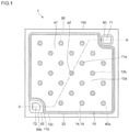
FIG. 1 is a schematic top view of some of the constituent elements of a light emitting element according to a first embodiment of the present disclosure. -
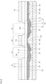
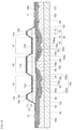
FIG. 2 is a schematic cross-sectional view taken along line II-II inFIG. 1 . -
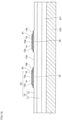
FIG. 3 is an enlarged schematic cross-sectional view of a portion of the semiconductor stack in the light emitting element according to the first embodiment of the present disclosure. -
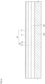
FIG. 4 is a schematic cross-sectional view showing a process in a method of manufacturing a light emitting element according to the first embodiment of the present disclosure. -
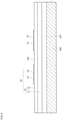
FIG. 5 is a schematic cross-sectional view showing a process in the method of manufacturing a light emitting element according to the first embodiment of the present disclosure. -
FIG. 6 is a schematic cross-sectional view showing a process in the method of manufacturing a light emitting element according to the first embodiment of the present disclosure. -
FIG. 7 is a schematic cross-sectional view showing a process in the method of manufacturing a light emitting element according to the first embodiment of the present disclosure. -
FIG. 8 is a schematic cross-sectional view showing a process in the method of manufacturing a light emitting element according to the first embodiment of the present disclosure. -
FIG. 9 is a schematic cross-sectional view showing a process in the method of manufacturing a light emitting element according to the first embodiment of the present disclosure. -
FIG. 10 is a schematic cross-sectional view showing a process in the method of manufacturing a light emitting element according to the first embodiment of the present disclosure. -
FIG. 11 is a schematic cross-sectional view showing another process in the method of manufacturing a light emitting element of the first embodiment of the present disclosure. -
FIG. 12 is a schematic cross-sectional view of a light emitting element obtained after the process shown inFIG. 11 . -
FIG. 13 is a schematic cross-sectional view of a light emitting element according to a second embodiment of the present disclosure. -
FIG. 14 is a schematic cross-sectional view of a light emitting element according to a third embodiment of the present disclosure. -
FIG. 15 is a schematic cross-sectional view of a variation of the light emitting element according to the first embodiment -
FIG. 16 is a schematic cross-sectional view showing a process in a method of manufacturing another variation of the light emitting element according to the first embodiment -
FIG. 17 is a schematic cross-sectional view showing a process in a method of manufacturing another variation of the light emitting element according to the first embodiment -
FIG. 18 is a schematic cross-sectional view showing a process in a method of manufacturing another variation of the light emitting element according to the first embodiment -
FIG. 19 is a schematic cross-sectional view of another variation of the light emitting element according to the first embodiment - Certain embodiments of the present disclosure will be explained below with reference to the accompanying drawings. In the drawings, the same reference numerals denote the same elements.
-
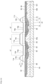
FIG. 1 is a schematic top view of some of the constituent elements of a light emitting element 1 according to a first embodiment of the present disclosure.FIG. 2 is a schematic cross-sectional view showing only the end faces along line II-II inFIG. 1 . - The light emitting element 1 has a
support substrate 100 and asemiconductor stack 20 disposed on thesupport substrate 100. -
FIG. 3 is an enlarged schematic cross-sectional view of a portion of thesemiconductor stack 20. - The
semiconductor stack 20 has a first conductivitytype semiconductor layer 10, a second conductivitytype semiconductor layer 15, and anactive layer 14. Theactive layer 14 is disposed between the first conductivitytype semiconductor layer 10 and the second conductivitytype semiconductor layer 15 and is an emission layer that emits light For example, the peak wavelength of the light from theactive layer 14 is no more than 400 nm, specifically 210 nm to 400 nm, more specifically 300 nm to 400 nm. For example, theactive layer 14 emits ultraviolet light Because the thickness of theactive layer 14 is smaller than the thicknesses of the first conductivitytype semiconductor layer 10 and the second conductivitytype semiconductor layer 15, it is indicated by a line inFIG. 2 . Similarly, theactive layer 14 is shown as a line inFIGS. 4 to 13 andFIGS. 15 to 19 . - The first conductivity
type semiconductor layer 10, the second conductivitytype semiconductor layer 15, and theactive layer 14 are each formed of a nitride semiconductor layer. Nitride semiconductors include semiconductors of all compositions represented by the chemical formula, InxAlyGa1-x-yN (0≤x≤1, 0≤y≤1, x+y≤1) with varied x and y percentages within the ranges. The first conductivitytype semiconductor layer 10 is a nitride semiconductor layer containing Al and Ga, for example, an AlGaN layer. The first conductivitytype semiconductor layer 10 is, for example, an n-type semiconductor layer. The first conductivitytype semiconductor layer 10 contains as an n-type impurity Si, for example. The second conductivitytype semiconductor layer 15 is, for example, a p-type semiconductor layer. The second conductivitytype semiconductor layer 15 contains as a p-type impurity Mg, for example. - The first conductivity
type semiconductor layer 10 has afirst layer 11 and asecond layer 12. Thefirst layer 11 and thesecond layer 12 are, for example, AlGaN layers. The Al percentage composition of thefirst layer 11 is smaller than the Al percentage composition of thesecond layer 12. For example, the Al percentage composition of thefirst layer 11 is in a range of 1% to 3%. The Al percentage composition of thesecond layer 12 is in a range of 3% to 5%. The Al percentage composition difference between thefirst layer 11 and thesecond layer 12 is preferably in a range of 1 % to 4%. For example, the Al percentage composition of thefirst layer 11 is 3%, and the Al percentage composition of thesecond layer 12 is 5%. - The first conductivity
type semiconductor layer 10 has a first region a1 and a second region a2. The first region a1 and the second region a2 each have asecond layer 12. Thesecond layer 12,active layer 14 and the second conductivitytype semiconductor layer 15 are stacked in the first region a1. Theactive layer 14 and the second conductivitytype semiconductor layer 15 are successively stacked on the face of thesecond layer 12 on thesupport substrate 100 side in the first region a1. - There is no
first layer 11 in the first region a1. Thefirst layer 11 is not disposed on thefirst face 12a of thesecond layer 12 in the first region a1. Thefirst face 12a of thesecond layer 12 is positioned, relative to thesecond layer 12, on the opposite side to thesupport substrate 100 in the first region a1, i.e., thefirst face 12a is exposed from thefirst layer 11. Thefirst face 12a functions as a primary light extraction face. In a top view, the first region a1 is a region where thefirst face 12a is located. In a cross-sectional view, the first region a1 is the portion of the first conductivitytype semiconductor layer 10 located immediately under thefirst face 12a. - The
first layer 11 and thesecond layer 12 are stacked in the second regions a2, but neither anactive layer 14 nor second conductivitytype semiconductor layer 15 is stacked. The face (second face) 12b of thesecond layer 12 on thesupport substrate 100 side in the second regions a2 is exposed from the second conductivitytype semiconductor layer 15 and theactive layer 14. Thesecond face 12b functions as a contact face with the firstconductive member 40 described later. In the top view, a second region a2 is a region where asecond face 12b is located. In a cross-sectional view, the second region a2 is a portion of the first conductivitytype semiconductor layer 10 that is located immediately above thesecond face 12b. - As shown in
FIG. 1 , in a top view, a plurality of second regions a2 are arranged in island shapes, and the second regions a2 are surrounded by the first region a1. In a top view, the area of the first region a1 is larger than the sum of the areas of the second regions a2. - In the example shown in
FIG. 3 , there is a third region a3 between the first region a1 and the second region a2. In the third region a3, thefirst layer 11, thesecond layer 12, theactive layer 14, and the second conductivitytype semiconductor layer 15 are stacked. The third region a3, positioned between the first region a1 and the second region a2, includes at least afirst layer 11 and asecond layer 12. The first region a1 and the second region a2 can be made continuous by removing theactive layer 14 and the second conductivitytype semiconductor layer 15 in the third region a3. - The
first layer 11 and thesecond layer 12 are stacked in the second regions a2. In the first region a1, asecond layer 12 is disposed, but nofirst layer 11 is disposed. In the example shown inFIG. 2 , the thickness of the first conductivitytype semiconductor layer 10 in the first region a1 is smaller than the thickness of the first conductivitytype semiconductor layer 10 in the second regions a2. The thickness of the first conductivitytype semiconductor layer 10 in the first region a1 or the second regions a2 means the maximum thickness of the first conductivitytype semiconductor layer 10 in the first region a1 or the second regions a2. - The thickness of the
second layer 12 in the second regions a2 is preferably smaller than the thickness of thefirst layer 11 in the second regions a2. For example, the thickness of thesecond layer 12 in the second regions a2 is preferably no more than 80%, more preferably no more than 70% of the thickness of thefirst layer 11 in the second regions a2. The thickness of thefirst layer 11 in the second regions a2 is preferably, for example, 0.3 µm to 3 µm, more preferably 1 µm to 2.5 µm. For example, the thickness of thesecond layer 12 in the second regions a2 is preferably 0.3 µm to 1.5 µm, more preferably 0.5 µm to 1.2 µm. As shown inFIG. 15 , the thickness of thefirst layer 11 can be set to be the same as the thickness of thesecond layer 12. In the present application, the thickness of thefirst layer 11 in the second regions a2 means the maximum thickness of thefirst layer 11 in the second regions a2. The thickness of thesecond layer 12 in the second regions a2 means the maximum thickness of thesecond layer 12 in the second regions a2. - The
first layer 11 in the second regions a2 has athird face 11a opposite the face on which thesecond layer 12 is stacked. There is a height difference between thefirst face 12a of thesecond layer 12 in the first region a1 and thethird face 11 a of thefirst layer 11 in the second region a2. As shown inFIG. 1 , in the top view, the outer edge of thethird face 11 a in the second region is positioned between the n-sideconductive part 40a of the firstconductive member 40 and the outer edge of thereflective electrode 30. - The
first face 12a of thesecond layer 12 in the first region a1 is roughened whereby protrusions and depressions are formed on thefirst face 12a. Thethird face 11 a of thefirst layer 11 in the second region a2 is roughened whereby protrusions and depressions are formed on thethird face 11a. The sizes of the protrusions and depressions of thefirst face 12a and thethird face 11 a are smaller than the height difference between thefirst face 12a and thethird face 11a. - The protrusions and depressions of the
first face 12a include a plurality offirst protrusions 10a. The protrusions and depressions of thethird face 11a include a plurality ofsecond protrusions 10b. The arithmetic mean height of thefirst protrusions 10a is greater than the arithmetic mean height of thesecond protrusions 10b. Thefirst protrusions 10a and thesecond protrusions 10b are, for example, cone or pyramid shaped. Thefirst protrusions 10a and thesecond protrusions 10b are triangular shaped in the cross section inFIG. 3 , and the height of each of thefirst protrusions 10a and thesecond protrusions 10b is represented by the height of the triangular shape. - As shown in
FIG. 2 , thefirst layer 11 and thesecond layer 12 are stacked in the peripheral portion of the first conductivitytype semiconductor layer 10. Neither anactive layer 14 nor second conductivitytype semiconductor layer 15 is stacked in the peripheral portion. Thesecond layer 12 has afourth face 12c exposed from theactive layer 14 and the second conductivitytype semiconductor layer 15. Thefourth face 12c surrounds the area in which the first region a1 and the second regions a2 are formed in the top view inFIG. 1 . Thefifth face 11 b is the surface of thefirst layer 11 in the peripheral portion of the first conductivitytype semiconductor layer 10 and is also roughened, whereby a plurality ofsecond protrusions 10b are formed on thefifth face 11b. The arithmetic mean height of thefirst protrusions 10a in the first region a1 is greater than the arithmetic mean height of thesecond protrusions 10b on thefifth face 11 b in the peripheral portion of the first conductivitytype semiconductor layer 10. - The light emitting element 1 further has a first
conductive member 40, a secondconductive member 50, a thirdconductive member 60, areflective electrode 30, afirst pad electrode 71, asecond pad electrode 72, and first to fourth insulatingfilms 81 to 84. - A
reflective electrode 30 is disposed on the surface (opposite the face on which theactive layer 14 is stacked) of the second conductivitytype semiconductor layer 15. Thereflective electrode 30 is in contact with the surface of the second conductivitytype semiconductor layer 15. Thereflective electrode 30 is electrically connected to the second conductivitytype semiconductor layer 15. Thereflective electrode 30 preferably has high reflectivity relative to the light emitted by theactive layer 14. Thereflective electrode 30 is, for example, a metal layer containing Ag. In the present application, thereflective electrode 30 having high reflectivity relative to the light emitted by theactive layer 14 means having a reflectance of at least 70%, and preferably at least 80%, relative to the wavelength of the light from theactive layer 14. - The surface of the second conductivity
type semiconductor layer 15 also has a region in which thereflective electrode 30 is not disposed. The region is covered by a first insulatingfilm 81. Furthermore, the first insulatingfilm 81 also covers a portion of thereflective electrode 30. The first insulatingfilm 81 is, for example, a silicon nitride film or silicon oxide film. - A second insulating
film 82 covers the first insulatingfilm 81. The second insulatingfilm 82 also covers thefourth face 12c of the first conductivitytype semiconductor layer 10, the lateral faces of theactive layer 14, and the lateral faces of the second conductivitytype semiconductor layer 15. The second insulatingfilm 82 is, for example, a silicon oxide film - A second
conductive member 50 is disposed on the surface of the second insulatingfilm 82. The secondconductive member 50 is, for example, a metal layer containing at least either Al or Cu. The secondconductive member 50 has a p-sideconductive part 50a. - The
reflective electrode 30 has a surface exposed from the first insulatingfilm 81 and the second insulatingfilm 82. Thereflective electrode 30 is in contact with the p-sideconductive part 50a of the secondconductive member 50. The secondconductive member 50 is electrically connected via the p-sideconductive part 50a and thereflective electrode 30 to the second conductivitytype semiconductor layer 15 stacked in the first region a1. - A third insulating
film 83 covers the secondconductive member 50. The thirdinsulating film 83 is, for example, a silicon oxide film. - A first
conductive member 40 is disposed on the surface of the third insulatingfilm 83. The firstconductive member 40 is, for example, a metal layer containing at least either Al or Cu. The firstconductive member 40 has an n-sideconductive part 40a. - A portion of the
second face 12b of thesecond layer 12 in the second region a2 is covered by the second insulatingfilm 82. Thesecond face 12b is formed to have, for example, a circular shape in a top view, and the first insulatingfilm 81 is formed outward from the outer edge of thesecond face 12b. The portion of thesecond face 12b, including its center, is exposed from the first insulatingfilm 81 and in contact with the n-sideconductive part 40a of the firstconductive member 40. The firstconductive member 40 is electrically connected to the first conductivitytype semiconductor layer 10 via the n-sideconductive part 40a. - The third
insulating film 83 is disposed between the firstconductive member 40 and the secondconductive member 50, and the firstconductive member 40 and the secondconductive member 50 are insulated and separated from one another by the third insulatingfilm 83. - As shown in
FIG. 1 , thesupport substrate 100 is square shaped in a top view. Afirst pad electrode 71 and asecond pad electrode 72 are arranged at diagonal positions on thesupport substrate 100. Thesemiconductor stack 20 in a top view is formed to have a substantially square shape without the two diagonal corners where thefirst pad electrode 71 and thesecond pad electrode 72 are arranged. - As shown in
FIG. 2 , the firstconductive member 40 has apad connection part 40b positioned under thefirst pad electrode 71. A thirdconductive member 60 is disposed on thepad connection part 40b. The thirdconductive member 60 can be formed, for example, by using the same materials and the same process as those for forming the secondconductive member 50. The thirdconductive member 60 is formed as an island shape separated from the secondconductive member 50. Thefirst pad electrode 71 is disposed on the thirdconductive member 60. Thefirst pad electrode 71 is electrically connected to the firstconductive member 40 via the thirdconductive member 60. - The second
conductive member 50 has apad connection part 50b positioned under thesecond pad electrode 72. Thesecond pad electrode 72 is disposed on thepad connection part 50b and is electrically connected to the secondconductive member 50. - The
first pad electrode 71 and thesecond pad electrode 72, for example, contains at least one metal selected from the group consisting of Ti, Pt, and Au. - The first
conductive member 40 is bonded to thesupport substrate 100 via thebonding layer 101. Thebonding layer 101 is a metal layer that contains a soldering material such as Sn. Thesupport substrate 100, for example, is a silicon substrate. - The upper face and the lateral faces of the
semiconductor stack 20 are covered by a fourth insulatingfilm 84. The upper face of thesemiconductor stack 20 includes thefirst face 12a of thesecond layer 12 in the first region a1, thethird face 11 a of thefirst layer 11 in the second regions a2, and thefifth face 11 b of thefirst layer 11 in the peripheral portion. The fourth insulatingfilm 84 is, for example, a silicon oxide film. - The surface of the fourth insulating
film 84 that covers the protrusions and depressions (including thefirst protrusions 10a) formed on thefirst face 12a in the first region a1, also has protrusions and depressions. The surface of the fourth insulatingfilm 84 that covers the protrusions and depressions (including thesecond protrusions 10b) formed on thethird face 11 a in the second regions a2, also has protrusions and depressions. The surface of the fourth insulatingfilm 84 that covers the protrusions and depressions (including thesecond protrusions 10b) formed on thefifth face 11 b of thefirst layer 11 in the peripheral portion of the first conductivitytype semiconductor layer 10, also has protrusions and depressions. - The arithmetic mean height of the protrusions formed on the surface of the fourth insulating
film 84 in the first region a1 is greater than the arithmetic mean height of the protrusions formed on the surface of the fourth insulatingfilm 84 in the second regions a2. The arithmetic mean height of the protrusions formed on the surface of the fourth insulatingfilm 84 in the first region a1 is greater than the arithmetic mean height of the protrusions formed on the surface of the fourth insulatingfilm 84 in the peripheral portion of the first conductivitytype semiconductor layer 10. Forming protrusions having a greater arithmetic mean height on the surface of the fourth insulatingfilm 84 in the first region a1 having anactive layer 14 stacked thereon and having a large contribution to the light extraction efficiency may improve the light extraction efficiency. - The light emitted by the
active layer 14 propagates through the first conductivitytype semiconductor layer 10 to be extracted from thesemiconductor stack 20. Because thesecond layer 12 has a higher Al percentage composition than Al percentage composition of thefirst layer 11 in the first conductivitytype semiconductor layer 10, the light absorption rate in thesecond layer 12 is lower than the light absorption rate in thefirst layer 11. In the case in which the light emitted by theactive layer 14 has a relatively short wavelength with a peak wavelength of no more than 400 nm, in particular, employing AlGaN having a high Al percentage composition for the first conductivitytype semiconductor layer 10 can reduce the light absorption by the first conductivitytype semiconductor layer 10 as compared to using GaN for the first conductivitytype semiconductor layer 10. The light absorption in the first region a1 where theactive layer 14 is stacked has a greater impact on the efficiency in extracting light from thesemiconductor stack 20 than the light absorption in the second regions a2 where noactive layer 14 is stacked. Accordingly, not disposing a first layer having higher light absorption than light absorption of thesecond layer 12 in the first region a1 can improve the light extraction efficiency as compared to the case in which afirst layer 11 is disposed in the first region a1. - Because no
first layer 11 is disposed in the first region a1, the thickness of the first conductivitytype semiconductor layer 10 in the first region a1 is smaller than the thickness of the first conductivitytype semiconductor layer 10 in the second regions a2. Reducing the thickness of the first conductivitytype semiconductor layer 10 in the first region a1, which greatly affects the light extraction efficiency, can reduce the light absorption in the first region a1, thereby increasing the light extraction efficiency. - In the second regions a2, the first
conductive member 40 is connected to the first conductivitytype semiconductor layer 10, providing a current conducting part for the first conductivitytype semiconductor layer 10. Forming not only asecond layer 12, but also afirst layer 11 that has a lower Al percentage composition than thesecond layer 12 in the second regions a2 can reduce the forward voltage (drive voltage) Vf as well as reducing the current concentration in the second regions a2 as compared to the case in which nofirst layer 11 is disposed in the second regions a2. Furthermore, making the thickness of the first conductivitytype semiconductor layer 10 in the second regions a2 larger than the thickness of the first conductivitytype semiconductor layer 10 in the first region a1 can reduce the resistance of the second regions a2 thereby lowering the Vf. - The higher the Al percentage composition in a nitride semiconductor layer containing Al and Ga, the higher the crack occurrence in the nitride semiconductor layer tends to be. The larger the thickness of a nitride semiconductor layer containing Al and Ga, the higher the crack occurrence in the nitride semiconductor layer tends to be. According to this embodiment, the thickness of the
second layer 12 having a higher Al percentage composition is thinner than thefirst layer 11. This can reduce the crack occurrence in the first conductivitytype semiconductor layer 10. - For the purpose of reducing the light absorption in the first region a1, lowering the Vf in the second regions a2, and reducing the crack occurrence in the first conductivity
type semiconductor layer 10, the Al percentage composition in the first conductivitytype semiconductor layer 10 is preferably in a range of 1 % to 5%. Furthermore, the thickness of thesecond layer 12 in the second regions a2 is preferably smaller than the thickness of thefirst layer 11 in the second regions a2. For example, the thickness of thesecond layer 12 in the second regions a2 is preferably no more than 80% of the thickness of thefirst layer 11 in the second regions a2. Making the thickness of thesecond layer 12 in the second regions a2 smaller than the thickness of thefirst layer 11 in the second regions a2 can reduce the crack occurrence in the first conductivitytype semiconductor layer 10 while lowering the Vf in the second regions a2. - Because a portion of the light extracted from the first region a1 may be absorbed by the
first layer 11 disposed in the second regions a2, it is preferable to have a distance between the first region a1 and the second regions a2 to reduce the light absorption. On the other hand, providing too much distance between the first region a1 and the second regions a2 reduces the area of the second region a2 in a top view and may allow the current to concentrate in the second regions a2. According to this embodiment, the outer edge of thethird face 11 a is positioned between the outer edge of the n-sideconductive part 40a of the firstconductive member 40 and the outer edge of thereflective electrode 30 in the top view. This can reduce the light absorption by thefirst layer 11 in the second regions a2 while hindering the current from concentrating in the second regions a2. - The first
conductive member 40 can be electrically connected to thefourth face 12c of thesecond layer 12 in the peripheral portion of the first conductivitytype semiconductor layer 10. In this case, disposing not only asecond layer 12, but also afirst layer 11 having a smaller Al percentage composition than thesecond layer 12 in the peripheral portion of the first conductivitytype semiconductor layer 10 can lower the Vf as compared to the case in which afirst layer 11 is not disposed in the peripheral portion. This can also reduce the crack occurrence in the peripheral portion. - Next, a method of manufacturing a light emitting element 1 according to the first embodiment of the present disclosure will be explained with reference to
FIG. 4 to FIG. 11 . - As shown in
FIG. 4 , on asubstrate 200, anunderlayer 201 including, for example, an undoped GaN layer, is grown. The thickness of theunderlayer 201 is, for example, 6 µm to 8 µm. Then asemiconductor stack 20 is formed via theunderlayer 201. Thesubstrate 200 is a substrate for allowing nitride semiconductor layers to grow, for example, a sapphire substrate. A buffer layer formed of, for example, AlGaN or AlN, can be formed on thesubstrate 200 before allowing theunderlayer 201 to grow. - The
semiconductor stack 20 includes a first conductivitytype semiconductor layer 10, anactive layer 14, and a second conductivitytype semiconductor layer 15. The first conductivitytype semiconductor layer 10 includes afirst layer 11 and asecond layer 12. On theunderlayer 201, thefirst layer 11, thesecond layer 12, theactive layer 14, and the second conductivitytype semiconductor layer 15 are successively epitaxially grown. For example, MOCVD (metal organic chemical vapor deposition) technique can be used to form the semiconductor layers included in thesemiconductor stack 20. - As described earlier, the first conductivity
type semiconductor layer 10 is a nitride semiconductor layer containing Al and Ga in which thefirst layer 11 has a lower Al percentage composition than the Al percentage composition of thesecond layer 12. For example, the Al percentage composition of thefirst layer 11 is 3%, and the Al percentage composition of thesecond layer 12 is 5%. - In forming the
semiconductor stack 20, it is preferable to form thefirst layer 11 to a thickness of, for example, 0.3 µm to 3 µm, more preferably 1 µm to 2.5 µm. For example, it is preferable to form thesecond layer 12 to a thickness of 0.3 µm to 1.5 µm, more preferably 0.5 µm to 1.2 µm. For example, the thickness of thefirst layer 11 is set to be 2 µm, and the thickness of thesecond layer 12 is set to be 1 µm. Forming thesecond layer 12, which has a higher Al percentage composition than thefirst layer 11, thinner than thefirst layer 11 can reduce the crack occurrence when the first conductivitytype semiconductor layer 10 is grown. - After forming the
semiconductor stack 20, as shown inFIG. 5 , the second conductivitytype semiconductor layer 15 and theactive layer 14 are partially removed. For example, the second conductivitytype semiconductor layer 15 and theactive layer 14 are partially removed by RIE (reactive ion etching). The partial removal of the second conductivitytype semiconductor layer 15 and theactive layer 14 exposes portions of thesecond layer 12 of the first conductivitytype semiconductor layer 10 from the second conductivitytype semiconductor layer 15 and theactive layer 14. - The first region a1 is where the second conductivity
type semiconductor layer 15 and theactive layer 14 remain unremoved. The second region a2 is located at the second layer 12 (thesecond face 12b that will serve as the conductive part for the first conductivity type semiconductor layer 10) exposed from the second conductivitytype semiconductor layer 15 and theactive layer 14. - Subsequently, in the state in which the
semiconductor stack 20 is formed on thesubstrate 200, thereflective electrode 30, the first insulatingfilm 81, the second insulatingfilm 82, the secondconductive member 50, the thirdconductive member 60, the third insulatingfilm 83, and the firstconductive member 40 described earlier with reference toFIG. 2 are formed. Thereflective electrode 30, the first insulatingfilm 81, the second insulatingfilm 82, the secondconductive member 50, the thirdconductive member 60, the third insulatingfilm 83, and the firstconductive member 40 can be formed by, for example, sputtering, vapor deposition, or the like. The secondconductive member 50 and the thirdconductive member 60 can be formed by the same process. The p-sideconductive part 50a of the secondconductive member 50 is in contact with thereflective electrode 30, and the n-sideconductive part 40a of the firstconductive member 40 is in contact with thesecond face 12b of the first conductivitytype semiconductor layer 10. - Subsequently, as shown in
FIG. 6 , the firstconductive member 40 is bonded to thesupport substrate 100 via abonding layer 101. InFIG. 6 , the structure inFIG. 5 is flipped upside down. Thesemiconductor stack 20 is bonded to thesupport substrate 100 while being held by thesubstrate 200. - After bonding the
semiconductor stack 20 and thesupport substrate 100, thesubstrate 200 is removed, and theunderlayer 201 is further removed. This exposes the surface of thefirst layer 11 of the first conductivitytype semiconductor layer 10 as shown inFIG. 7 . - As shown in
FIG. 8 , amask 91 is formed on the surface of the exposedfirst layer 11, and the first conductivitytype semiconductor layer 10 is selectively removed by, for example, RIE. In the first conductivitytype semiconductor layer 10, nomask 91 is formed on thefirst layer 11 in the first region a1 where theactive layer 14 and the second conductivitytype semiconductor layer 15 are stacked. Thefirst layer 11 in the first region a1 is removed, and thesecond layer 12 in the first region a1 is exposed from thefirst layer 11. In this example, thefirst layer 11 in the first region a1 is entirely removed. - The
first layer 11 in the second region a2, which includes thesecond face 12b to which the n-sideconductive part 40a of the firstconductive member 40 is connected, is covered by themask 91 and not removed, allowing thesecond layer 12 and thefirst layer 11, which is thicker than thesecond layer 12 and has a lower Al percentage composition than thesecond layer 12, to remain. - The
mask 91 is also disposed in the area outward from the first region a1 of the first conductivitytype semiconductor layer 10, and thus thefirst layer 11 in the area outward from the first region a1 also remains unremoved. - After selectively removing the
first layer 11, themask 91 is removed. After removing themask 91, as shown inFIG. 9 , thefirst layer 11 and thesecond layer 12 in the area outward from the first region a1 are removed. A stack of thefirst layer 11 and thesecond layer 12 are maintained in a portion of the area outward from the first region a1 as the peripheral portion of the first conductivitytype semiconductor layer 10. In the area outward from the peripheral portion, the second insulatingfilm 82 is exposed from thefirst layer 11 and thesecond layer 12. - By following the processes up to this point, as shown in
FIG. 9 , the surface of thesecond layer 12 is exposed as thefirst face 12a in the first region a1, the surface of thefirst layer 11 is exposed as thethird face 11 a in the second region a2, and the surface of thefirst layer 11 is exposed as thefifth face 11 b in the peripheral portion. Subsequently, these surfaces are roughened. For example, TMAH (tetramethylammonium hydroxide) is used to roughen the surfaces. The thickness of thefirst layer 11 after roughening is, for example, preferably 0.3 µm to 3 µm, more preferably 1 µm to 2.5 µm. The thickness of thesecond layer 12 after roughening is, for example, preferably 0.3 µm to 1.5 µm, more preferably 0.5 µm to 1.2 µm. - As shown in
FIG. 10 , a plurality offirst protrusions 10a are formed on thefirst face 12a of thesecond layer 12 in the first region a1, and a plurality ofsecond protrusions 10b are formed on thethird face 11 a of thefirst layer 11 in the second region a2 and thefifth face 11 b of thefirst layer 11 in the peripheral portion. - In wet etching a nitride semiconductor layer containing Al and Ga using TMAH, the higher the Al percentage composition, the higher the etching rate and the greater the surface roughness tend to be. Because the Al percentage composition of the
second layer 12 is higher than the Al percentage composition of thefirst layer 11, the arithmetic mean height of thefirst protrusions 10a formed on thefirst face 12a of thesecond layer 12 is greater than the arithmetic mean height of thesecond protrusions 10b formed on thethird face 11a and thefifth face 11 b of thefirst layer 11. By creating higherfirst protrusions 10a on thefirst face 12a in the first region a1 that has anactive layer 14 and a large contribution to the light extraction efficiency, the light extraction efficiency may be increased. - On the other hand, because the Al percentage composition of the
first layer 11 is lower than the Al percentage composition of thesecond layer 12, the etching rate for thefirst layer 11 in wet etching tends to be lower than the etching rate for thesecond layer 12. Reducing the etched amount of thethird face 11 a in the second region a2 can moderate the reduction in the thickness of thefirst layer 11 in the second region a2. Because the Al percentage composition of thefirst layer 11 is lower than Al percentage composition of thesecond layer 12, moderating the reduction in the thickness of thefirst layer 11 in the second region a2 connected to the n-sideconductive part 40a of the firstconductive member 40 can, as described earlier, reduce the forward voltage (drive voltage) Vf. - After roughening the surface of the first conductivity
type semiconductor layer 10, a fourth insulatingfilm 84 is formed to cover the first conductivitytype semiconductor layer 10 and the second insulatingfilm 82. Subsequently, a portion of the second insulatingfilm 82 and a portion of the fourth insulatingfilm 84 that are located in the area outward from the first conductivitytype semiconductor layer 10 are removed. This, as shown inFIG. 2 , exposes a portion of the secondconductive member 50 from the second insulatingfilm 82 as apad connection part 50b, and asecond pad electrode 72 is formed on thepad connection part 50b. Furthermore, a portion of the thirdconductive member 60 is exposed from the second insulatingfilm 82, and afirst pad electrode 71 is formed on the thirdconductive member 60. - In the process described earlier with reference to
FIG. 8 , after removing thefirst layer 11 in the first region a1 using themask 91 to expose thefirst face 12a of thesecond layer 12 in the first region a1 from thefirst layer 11, thefirst face 12a of thesecond layer 12 in the first region a1 can be roughened by etching with, for example, TMAH while maintaining themask 91 that covers thethird face 11 a of thefirst layer 11 in the second region a2. - Roughening while covering the
third face 11 a of thefirst layer 11 in the second region a2 with themask 91 can create a plurality offirst protrusions 10a on thefirst face 12a of thesecond layer 12 in the first region a1, but does not create protrusions or depressions on thethird face 11 a of thefirst layer 11 in the second region a2 covered by themask 91 as shown inFIG. 11 . Themask 91 used in removing thefirst layer 11 in the first region a1 can be utilized in roughening thefirst face 12a of thesecond layer 12 in the first region a1, thereby simplifying the process. Such a roughening process allows thethird face 11 a of thefirst layer 11 in the second region a2 to be unetched to remain flat as shown inFIG. 12 . This can make thefirst layer 11 in the second region a2 thicker, thereby reducing the Vf. -
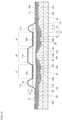
FIG. 13 is a schematic cross-sectional view of a light emitting element according to a second embodiment of the present disclosure. The light emitting element according to the second embodiment has the same structure as the first embodiment shown inFIG. 2 except for the features described below. Only the differences from the first embodiment will basically be descried below. - In this embodiment, the first conductivity
type semiconductor layer 10 has athird layer 13 in addition to thefirst layer 11 and thesecond layer 12. Thethird layer 13 is also a nitride semiconductor layer containing Al and Ga, for example, an AlGaN layer. The Al percentage composition of thesecond layer 12 is higher than the Al percentage composition of thefirst layer 11, and the Al percentage composition of thethird layer 13 is higher than the Al percentage composition of thesecond layer 12. The Al percentage composition difference between thefirst layer 11 and thesecond layer 12 is preferably in a range of 1 % to 4%. The Al percentage composition difference between thesecond layer 12 and thethird layer 13 is preferably more than 0% and up to 4%. For example, the Al percentage composition of thefirst layer 11 is 3%, the Al percentage composition of thesecond layer 12 is 4%, and the Al percentage composition of thethird layer 13 is 5%. From the standpoint of hindering the first conductivitytype semiconductor layer 10 from absorbing light, the Al percentage composition difference between thefirst layer 11 and thesecond layer 12 is preferably at least 2%. For example, the Al percentage composition of thefirst layer 11 is set as 3%, the Al percentage composition of thesecond layer 12 is set as 5%, and the Al percentage composition of thethird layer 13 is set as 6%. - In this embodiment, the
first layer 11, thesecond layer 12, and thethird layer 13 are successively formed on thesubstrate 200, for example, via anunderlayer 201. Anactive layer 14 is formed on thethird layer 13, and a second conductivitytype semiconductor layer 15 is formed on theactive layer 14. - In the first region a1, the
second layer 12 having a higher Al percentage composition than thefirst layer 11 and thethird layer 13 having a higher Al percentage composition than thesecond layer 12 are disposed, but nofirst layer 11 is disposed. Not disposing afirst layer 11 having a lower Al percentage composition and higher light absorption than the second andthird layers first layer 11 is disposed in the first region a1. By disposing thethird layer 13 having a higher Al percentage composition and lower light absorption than thesecond layer 12 as a layer more closely positioned to theactive layer 14 than thesecond layer 12 can further reduce the light absorption in the first region a1. - Because no
first layer 11 is disposed in the first region a1, the thickness of the first conductivitytype semiconductor layer 10 in the first region a1 is smaller than the thickness of the first conductivitytype semiconductor layer 10 in the second region a2. Reducing the thickness of the first conductivitytype semiconductor layer 10 in the first region a1, which has a large impact on the light extraction efficiency, can reduce the light absorption in the first region a1, thereby improving the light extraction efficiency. - The
first layer 11, thesecond layer 12, and thethird layer 13 are stacked in the second region a2. Neither anactive layer 14 nor second conductivitytype semiconductor layer 15 is stacked in the second region a2. The face (sixth face) 13a of thethird layer 13 on thesupport substrate 100 side in the second region a2 is exposed from the second conductivitytype semiconductor layer 15 and theactive layer 14. The n-sideconductive part 40a of the firstconductive member 40 is in contact with thesixth face 13a. - Allowing the second region a2 to also have the
first layer 11 having a lower Al percentage composition than thesecond layer 12 and thethird layer 13 can reduce the forward voltage (drive voltage) Vf and reduce the current concentration in the second region a2 as compared to the case in which the second region a2 has nofirst layer 11. Furthermore, making the first conductivitytype semiconductor layer 10 in the second region a2 thicker than the first conductivitytype semiconductor layer 10 in the first region a1 can reduce the resistance of the second region a2, thereby reducing the Vf. -
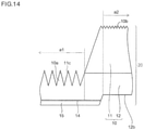
FIG. 14 is a schematic cross-sectional view of a light emitting element according to a third embodiment of the present disclosure.FIG. 14 , similar toFIG. 3 described earlier, is an enlarged schematic cross section of a portion of thesemiconductor stack 20. - According to the third embodiment,
portions 11 c of thefirst layer 11 are provided in the first region a1. The thickness of aportion 11 c of thefirst layer 11 in the first region a1 is smaller than the thickness of thesecond layer 12 in the first region a1, and smaller than the thickness of thefirst layer 11 in the second region a2. The thickness of aportion 11 c of thefirst layer 11 in the first region a1 means the maximum thickness of theportion 11 c of thefirst layer 11 in the first region a1. - In the third embodiment, the
first layer 11 in the first region a1 is partially removed, instead of being entirely removed, after exposing the surface of thefirst layer 11 in the process shown inFIG. 7 discussed earlier. The second region a2 is allowed to maintain thefirst layer 11 with a greater thickness than thefirst layer 11 in the first region a1. In the step of partially removing thefirst layer 11, by not entirely removing thefirst layer 11 in the first region a1, the first region a1 is allowed to maintain a thinnerfirst layer 11 than that in the second region a2 and thesecond layer 12. Subsequently, the surfaces of the first region a1 and the second region a2 are roughened by etching with TMAH, for example. - In the example shown in
FIG. 14 , theportions 11 c of thefirst layer 11 are located at the apexes of the cone or pyramid shapedfirst protrusions 10a on the surface of thesecond layer 12 in the first region a1. The thickness of thesecond portion 11 c of thefirst layer 11 is smaller than the height of thefirst protrusion 10a on thesecond layer 12. In the third embodiment, thefirst protrusion 10a has a trapezoidal shape in a cross-sectional view inFIG. 14 , and the height of thefirst protrusion 10a represents the height of the trapezoid Theportions 11 c of thefirst layer 11 each have a triangular shape in a cross-sectional view inFIG. 14 , and the thickness of aportion 11c of thefirst layer 11 represents the height of the triangle. - The
first layer 11 has a lower Al percentage composition and higher light absorption than thesecond layer 12, but limiting thefirst layer 11 in the first region a1 to theportions 11c that are thinner than thesecond layer 12 and thinner than thefirst layer 11 in the second region a2 can substantially eliminate the impact of the light absorption by thefirst layer 11 in the first region a1 on the light extraction efficiency. - Next, a method of manufacturing another variation of the light emitting element of the first embodiment will be explained with reference to
FIG. 16 to FIG. 18 . This variation is also applicable to the second embodiment and the third embodiment - After forming a
semiconductor stack 20 on asubstrate 200 as previously described with reference toFIG. 4 , a portion of the surface of the second conductivitytype semiconductor layer 15 can be modified as shown inFIG. 16 . InFIG. 16 and the subsequent drawings, the portions of the surface of the second conductivitytype semiconductor layer 15 marked with dot hatching are modified. For example, amask 500 is formed on a portion of the surface of the second conductivitytype semiconductor layer 15, which will be positioned above the first region a1 of the first conductivitytype semiconductor layer 10 described earlier. Then the surface of the second conductivitytype semiconductor layer 15 exposed from themask 500 is plasma treated in ambient air containing oxygen, for example. - The modified surface of the second conductivity
type semiconductor layer 15 has a higher resistance than the surface of the second conductivitytype semiconductor layer 15 that is not modified. In other words, on the surface of the second conductivitytype semiconductor layer 15, a low resistance portion (unmodified portion) 15a and a high resistance portion (modified portion) 15b having a higher resistance than that of thelow resistance portion 15a are formed. - Subsequently, as shown in
FIG. 17 , areflective electrode 30 is formed on the surface of the second conductivitytype semiconductor layer 15 so as to straddle thelow resistance portion 15a and thehigh resistance portion 15b. Thereflective electrode 30 is in contact with the entirelow resistance portion 15a. Thereflective electrode 30 is in contact with a portion of thehigh resistance portion 15b. The area of contact between thereflective electrode 30 and thelow resistance portion 15a is larger than the area of contact between thereflective electrode 30 and thehigh resistance portion 15b. After forming thereflective electrode 30, a first insulatingfilm 81 is formed to cover the surfaces of thereflective electrode 30 and the second conductivitytype semiconductor layer 15. - Subsequently, as shown in
FIG. 18 , a portion of the first insulatingfilm 81, a portion of the second conductivitytype semiconductor layer 15, and a portion of theactive layer 14 are removed. This partially exposes thesecond layer 12 of the first conductivitytype semiconductor layer 10 from the second conductivitytype semiconductor layer 15 and theactive layer 14. The surface of the remaining unremoved second conductivitytype semiconductor layer 15 includes thelow resistance portion 15a and thehigh resistance portion 15b. - Subsequently, the processes shown in
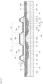
FIG. 6 and onward described earlier are followed to obtain the light emitting element shown inFIG. 19 . The surface of the second conductivitytype semiconductor layer 15 stacked in the first region a1 of the first conductivitytype semiconductor layer 10 includes thelow resistance portion 15a and thehigh resistance portion 15b. Thehigh resistance portion 15b includes a high resistance portion 15bc positioned closer to the second region a2 than thelow resistance portion 15a. Thehigh resistance portion 15b also includes ahigh resistance portion 15b positioned near the periphery of the first conductivitytype semiconductor layer 10. The current density of thehigh resistance portion 15b is lower than the current density of thelow resistance portion 15a. Accordingly, theactive layer 14 in the area where thelow resistance portion 15a is disposed tends to emit light more intensely than theactive layer 14 in the area where thehigh resistance portion 15b is disposed. - By positioning the
high resistance portion 15b in thesecond region 11a where thefirst layer 11 having higher light absorption than thesecond layer 12 of the first conductivitytype semiconductor layer 10 is disposed and in the peripheral area thereof, the emission in the area near thefirst layer 11 can be reduced to thereby reduce the light absorption by thefirst layer 11. Because thereflective electrode 30 is also in contact with thehigh resistance portion 15b, the light absorption by thefirst layer 11 may be reduced and the light extraction efficiency may be improved while maintaining the area of thereflective electrode 30. - In the cross section in
FIG. 19 , the width of a portion of thereflective electrode 30 where thehigh resistance portion 15b is in contact is preferably 3 µm to 25 µm, for example, more preferably 5 µm to 20 µm. - In the cross section in
FIG. 19 , the width of the high resistance portion 15ba of thehigh resistance portion 15b positioned closer to the periphery of the first conductivitytype semiconductor layer 10 is preferably larger than the width of the high resistance portion 15bc positioned closer to the second region a2. Making the width of the high resistance portion 15ba near the peripheral portion in which thefirst layer 11 is disposed more broadly than the second region a2 larger than that of the high resistance portion 15bc can improve the effect of reducing the light absorption by thefirst layer 11. - In the foregoing, certain embodiments of the present invention have been explained with reference to specific examples. The present invention, however, is not limited to these specific examples. Any form implementable by a person of ordinary skill in the art by suitably changing the design based on any of the embodiments descried above will fall within the scope of the present invention so long as it encompasses the subject matter of the present invention. In addition, various changes and modifications a person of ordinary skill in the art would be able to make under the ideas of the present invention would also fall within the scope of the present invention.
Claims (14)
- A light emitting element comprising:a semiconductor stack comprising:a first conductivity type semiconductor layer,a second conductivity type semiconductor layer, andan active layer disposed between the first conductivity type semiconductor layer and the second conductivity type semiconductor layer,a first conductive member electrically connected to the first conductivity type semiconductor layer, anda second conductive member electrically connected to the second conductivity type semiconductor layer; wherein:the first conductivity type semiconductor layer is a nitride semiconductor layer containing Al and Ga, the first conductivity type semiconductor layer comprises a first layer and a second layer, and an Al percentage composition of the first layer is lower than an Al percentage composition of the second layer,the first conductivity type semiconductor layer comprises:a first region where the second conductivity type semiconductor layer and the active layer are stacked; anda second region exposed from the second conductivity type semiconductor layer and the active layer, the second region being connected to the first conductive member; and(i) a thickness of the first layer in the first region is smaller than a thickness of the first layer in the second region, or (ii) the second layer is exposed from the first layer in the first region.
- The light emitting element according to claim 1, wherein:
a thickness of the second layer in the second region is smaller than the thickness of the first layer in the second region. - The light emitting element according to claim 1 or 2, wherein:
a thickness of the second layer in the second region is no more than 80% of the thickness of the first layer in the second region. - The light emitting element according to any of the preceding claims , wherein:
a plurality of first protrusions are formed on a surface of the second layer in the first region, and a plurality of second protrusions are formed on a surface of the first layer in the second region, wherein an arithmetic mean height of the first protrusions is greater than an arithmetic mean height of the second protrusions. - The light emitting element according to any of the preceding claims , wherein:
a peak wavelength of light from the active layer is no more than 400 nm. - The light emitting element according to any of the preceding claims , wherein:
the second conductive member is in contact with the second conductivity type semiconductor layer stacked in the first region. - A method of manufacturing a light emitting element, the method comprising:forming a semiconductor stack that comprises:a substrate,a first conductivity type semiconductor layer disposed on the substrate,an active layer disposed on the first conductivity type semiconductor layer, anda second conductivity type semiconductor layer disposed on the active layer, wherein:
the first conductivity type semiconductor layer is a nitride semiconductor layer containing Al and Ga, the first conductive type semiconductor layer comprises a first layer disposed on the substrate and a second layer disposed on the first layer, and an Al percentage composition of the first layer is lower than an Al percentage composition of the second layer,removing a portion of the second conductivity type semiconductor layer and a portion of the active layer, thereby exposing a portion of the first conductivity type semiconductor layer from the second conductivity type semiconductor layer and the active layer to form a first region and a second region in the first conductivity type semiconductor layer, wherein:the first region is a region where the second conductivity type semiconductor layer and the active layer remain unremoved, andthe second region includes the portion of the first conductivity type semiconductor layer that is exposed from the second conductivity type semiconductor layer and the active layer;subsequent to forming the first region and the second region, exposing a surface of the first layer of the first conductivity type semiconductor layer by removing the substrate; andsubsequent to exposing the surface of the first layer, removing at least a portion of the first layer in the first region, such that (i) a thickness of the first layer in the first region is smaller than a thickness of the first layer in the second region, or (ii) the second layer is exposed from the first layer in the first region. - The method of manufacturing a light emitting element according to claim 7, further comprising:
subsequent to removing said at least a portion of the first layer in the first region, forming a plurality of first protrusions on a surface of the second layer in the first region and a plurality of second protrusions on the surface of the first layer in the second region, wherein:
an arithmetic mean height of the first protrusions is greater than an arithmetic mean height of the second protrusions. - The method of manufacturing a light emitting element according to claim 7 or 8, further comprising:
subsequent to removing said at least a portion of the first layer in the first region, forming a plurality of first protrusions on the surface of the second layer in the first region, wherein:in removing said at least the portion of the first layer in the first region, at least the portion of the first layer in the first region is removed in the state in which the surface of the first layer in the second region is covered with a mask, andthe plurality of first protrusions are formed by etching the first region using the mask. - The method of manufacturing a light emitting element according to any of claims 7 to 9, wherein:
in forming the semiconductor stack, a thickness of the second layer is formed to be smaller than a thickness of the first layer. - The method of manufacturing a light emitting element according to any of claims 7 to 10, wherein:
in forming the semiconductor stack, the second layer is formed to have a thickness that is no more than 50% of the thickness of the first layer. - The method of manufacturing a light emitting element according to any of claims 7 to 11, wherein:
a peak wavelength of light from the active layer is no more than 400 nm. - The method of manufacturing a light emitting element according to any of claims 7 to 12, further comprising:forming a low resistance portion and a high resistance portion that has a higher resistance than the low resistance portion on the surface of the second conductivity type semiconductor layer on the first region of the first conductivity type semiconductor layer, wherein the high resistance portion is positioned closer to the second region than the low resistance portion is; andforming an electrode on the surface of the second conductivity type semiconductor layer such that an area of the electrode in contact with the low resistance portion is larger than an area of the electrode in contact with the high resistance portion.
- The method of manufacturing a light emitting element according to claim 13, wherein:
the high resistance portion is formed by plasma treating the surface of the second conductivity type semiconductor layer.
Applications Claiming Priority (2)
| Application Number | Priority Date | Filing Date | Title |
|---|---|---|---|
| JP2020124209 | 2020-07-21 | ||
| JP2021021054A JP7312953B2 (en) | 2020-07-21 | 2021-02-12 | Light-emitting element and method for manufacturing light-emitting element |
Publications (2)
| Publication Number | Publication Date |
|---|---|
| EP3944344A1 true EP3944344A1 (en) | 2022-01-26 |
| EP3944344B1 EP3944344B1 (en) | 2022-10-19 |
Family
ID=76807539
Family Applications (1)
| Application Number | Title | Priority Date | Filing Date |
|---|---|---|---|
| EP21183868.5A Active EP3944344B1 (en) | 2020-07-21 | 2021-07-06 | Light emitting element and method of manufacturing light emitting element |
Country Status (3)
| Country | Link |
|---|---|
| EP (1) | EP3944344B1 (en) |
| KR (1) | KR102952007B1 (en) |
| CN (1) | CN113964245A (en) |
Cited By (1)
| Publication number | Priority date | Publication date | Assignee | Title |
|---|---|---|---|---|
| EP4270497A3 (en) * | 2022-04-28 | 2023-11-08 | Nichia Corporation | Semiconductor light-emitting element |
Families Citing this family (1)
| Publication number | Priority date | Publication date | Assignee | Title |
|---|---|---|---|---|
| WO2025217793A1 (en) * | 2024-04-16 | 2025-10-23 | Jade Bird Display (shanghai) Limited | Micro led array and micro led display panel |
Citations (3)
| Publication number | Priority date | Publication date | Assignee | Title |
|---|---|---|---|---|
| JP2013084878A (en) | 2011-10-10 | 2013-05-09 | Lg Innotek Co Ltd | Light emitting device and lighting apparatus including the same |
| US20170263817A1 (en) * | 2015-04-03 | 2017-09-14 | Soko Kagaku Co., Ltd. | Nitride Semiconductor Ultraviolet Light-Emitting Element and Nitride Semiconductor Ultraviolet Light-Emitting Device |
| US20180130924A1 (en) * | 2016-11-09 | 2018-05-10 | Epistar Corporation | Light-emitting device and manufacturing method thereof |
Family Cites Families (1)
| Publication number | Priority date | Publication date | Assignee | Title |
|---|---|---|---|---|
| KR102407739B1 (en) * | 2017-11-24 | 2022-06-10 | 쑤저우 레킨 세미컨덕터 컴퍼니 리미티드 | Semiconductor device |
-
2021
- 2021-07-06 EP EP21183868.5A patent/EP3944344B1/en active Active
- 2021-07-12 KR KR1020210091054A patent/KR102952007B1/en active Active
- 2021-07-20 CN CN202110817607.9A patent/CN113964245A/en active Pending
Patent Citations (3)
| Publication number | Priority date | Publication date | Assignee | Title |
|---|---|---|---|---|
| JP2013084878A (en) | 2011-10-10 | 2013-05-09 | Lg Innotek Co Ltd | Light emitting device and lighting apparatus including the same |
| US20170263817A1 (en) * | 2015-04-03 | 2017-09-14 | Soko Kagaku Co., Ltd. | Nitride Semiconductor Ultraviolet Light-Emitting Element and Nitride Semiconductor Ultraviolet Light-Emitting Device |
| US20180130924A1 (en) * | 2016-11-09 | 2018-05-10 | Epistar Corporation | Light-emitting device and manufacturing method thereof |
Cited By (1)
| Publication number | Priority date | Publication date | Assignee | Title |
|---|---|---|---|---|
| EP4270497A3 (en) * | 2022-04-28 | 2023-11-08 | Nichia Corporation | Semiconductor light-emitting element |
Also Published As
| Publication number | Publication date |
|---|---|
| CN113964245A (en) | 2022-01-21 |
| EP3944344B1 (en) | 2022-10-19 |
| KR102952007B1 (en) | 2026-04-10 |
| KR20220011579A (en) | 2022-01-28 |
Similar Documents
| Publication | Publication Date | Title |
|---|---|---|
| US7154123B2 (en) | Nitride-based semiconductor light-emitting device | |
| US7348601B2 (en) | Nitride-based compound semiconductor light emitting device | |
| US7888144B2 (en) | Light-emitting device and method for making the same | |
| CN101305478A (en) | Nitride semiconductor light-emitting element and method for manufacturing nitride semiconductor light-emitting element | |
| US20110303938A1 (en) | Group III nitride semiconductor light-emitting element | |
| WO2005050748A1 (en) | Semiconductor device and method for manufacturing same | |
| US20090127568A1 (en) | Semiconductor light emitting element and method for fabricating the same | |
| EP3944344B1 (en) | Light emitting element and method of manufacturing light emitting element | |
| JP2013239471A (en) | Method of manufacturing light-emitting diode element | |
| US12243965B2 (en) | Semiconductor light-emitting element and method of manufacturing semiconductor light-emitting element | |
| JP7312953B2 (en) | Light-emitting element and method for manufacturing light-emitting element | |
| JP2007281037A (en) | Semiconductor light emitting element, and its manufacturing method | |
| JP2004228290A (en) | Semiconductor light emitting device and manufacturing method thereof | |
| JPH11354841A (en) | Fabrication of semiconductor light emitting element | |
| TW202013766A (en) | Semiconductor devices and manufacturing methods thereof | |
| JP2017055020A (en) | Manufacturing method of semiconductor device | |
| JP7534656B2 (en) | Light-emitting device manufacturing method and light-emitting device | |
| JP2007042952A (en) | Gallium nitride compound semiconductor light emitting device | |
| CN109860349B (en) | LED chip and manufacturing method thereof | |
| JP4174581B2 (en) | Method for manufacturing light emitting device | |
| JP5109363B2 (en) | Semiconductor light emitting device manufacturing method, semiconductor light emitting device, and light emitting device | |
| JPH07221347A (en) | Gallium nitride compound semiconductor light emitting device | |
| JP2009283762A (en) | Method for manufacturing nitride compound semiconductor led | |
| US20220029057A1 (en) | Light emitting element and method of manufacturing light emitting element | |
| US20230155081A1 (en) | Semiconductor light-emitting element and method for manufacturing semiconductor light-emitting element |
Legal Events
| Date | Code | Title | Description |
|---|---|---|---|
| PUAI | Public reference made under article 153(3) epc to a published international application that has entered the european phase |
Free format text: ORIGINAL CODE: 0009012 |
|
| STAA | Information on the status of an ep patent application or granted ep patent |
Free format text: STATUS: THE APPLICATION HAS BEEN PUBLISHED |
|
| AK | Designated contracting states |
Kind code of ref document: A1 Designated state(s): AL AT BE BG CH CY CZ DE DK EE ES FI FR GB GR HR HU IE IS IT LI LT LU LV MC MK MT NL NO PL PT RO RS SE SI SK SM TR |
|
| STAA | Information on the status of an ep patent application or granted ep patent |
Free format text: STATUS: REQUEST FOR EXAMINATION WAS MADE |
|
| 17P | Request for examination filed |
Effective date: 20220217 |
|
| RBV | Designated contracting states (corrected) |
Designated state(s): AL AT BE BG CH CY CZ DE DK EE ES FI FR GB GR HR HU IE IS IT LI LT LU LV MC MK MT NL NO PL PT RO RS SE SI SK SM TR |
|
| GRAP | Despatch of communication of intention to grant a patent |
Free format text: ORIGINAL CODE: EPIDOSNIGR1 |
|
| STAA | Information on the status of an ep patent application or granted ep patent |
Free format text: STATUS: GRANT OF PATENT IS INTENDED |
|
| RIC1 | Information provided on ipc code assigned before grant |
Ipc: H01L 33/20 20100101AFI20220601BHEP |
|
| INTG | Intention to grant announced |
Effective date: 20220623 |
|
| GRAS | Grant fee paid |
Free format text: ORIGINAL CODE: EPIDOSNIGR3 |
|
| GRAA | (expected) grant |
Free format text: ORIGINAL CODE: 0009210 |
|
| STAA | Information on the status of an ep patent application or granted ep patent |
Free format text: STATUS: THE PATENT HAS BEEN GRANTED |
|
| AK | Designated contracting states |
Kind code of ref document: B1 Designated state(s): AL AT BE BG CH CY CZ DE DK EE ES FI FR GB GR HR HU IE IS IT LI LT LU LV MC MK MT NL NO PL PT RO RS SE SI SK SM TR |
|
| REG | Reference to a national code |
Ref country code: GB Ref legal event code: FG4D |
|
| REG | Reference to a national code |
Ref country code: CH Ref legal event code: EP |
|
| REG | Reference to a national code |
Ref country code: DE Ref legal event code: R096 Ref document number: 602021000583 Country of ref document: DE |
|
| REG | Reference to a national code |
Ref country code: IE Ref legal event code: FG4D |
|
| REG | Reference to a national code |
Ref country code: AT Ref legal event code: REF Ref document number: 1526113 Country of ref document: AT Kind code of ref document: T Effective date: 20221115 |
|
| REG | Reference to a national code |
Ref country code: LT Ref legal event code: MG9D |
|
| REG | Reference to a national code |
Ref country code: NL Ref legal event code: MP Effective date: 20221019 |
|
| REG | Reference to a national code |
Ref country code: AT Ref legal event code: MK05 Ref document number: 1526113 Country of ref document: AT Kind code of ref document: T Effective date: 20221019 |
|
| PG25 | Lapsed in a contracting state [announced via postgrant information from national office to epo] |
Ref country code: NL Free format text: LAPSE BECAUSE OF FAILURE TO SUBMIT A TRANSLATION OF THE DESCRIPTION OR TO PAY THE FEE WITHIN THE PRESCRIBED TIME-LIMIT Effective date: 20221019 |
|
| PG25 | Lapsed in a contracting state [announced via postgrant information from national office to epo] |
Ref country code: SE Free format text: LAPSE BECAUSE OF FAILURE TO SUBMIT A TRANSLATION OF THE DESCRIPTION OR TO PAY THE FEE WITHIN THE PRESCRIBED TIME-LIMIT Effective date: 20221019 Ref country code: PT Free format text: LAPSE BECAUSE OF FAILURE TO SUBMIT A TRANSLATION OF THE DESCRIPTION OR TO PAY THE FEE WITHIN THE PRESCRIBED TIME-LIMIT Effective date: 20230220 Ref country code: NO Free format text: LAPSE BECAUSE OF FAILURE TO SUBMIT A TRANSLATION OF THE DESCRIPTION OR TO PAY THE FEE WITHIN THE PRESCRIBED TIME-LIMIT Effective date: 20230119 Ref country code: LT Free format text: LAPSE BECAUSE OF FAILURE TO SUBMIT A TRANSLATION OF THE DESCRIPTION OR TO PAY THE FEE WITHIN THE PRESCRIBED TIME-LIMIT Effective date: 20221019 Ref country code: FI Free format text: LAPSE BECAUSE OF FAILURE TO SUBMIT A TRANSLATION OF THE DESCRIPTION OR TO PAY THE FEE WITHIN THE PRESCRIBED TIME-LIMIT Effective date: 20221019 Ref country code: ES Free format text: LAPSE BECAUSE OF FAILURE TO SUBMIT A TRANSLATION OF THE DESCRIPTION OR TO PAY THE FEE WITHIN THE PRESCRIBED TIME-LIMIT Effective date: 20221019 Ref country code: AT Free format text: LAPSE BECAUSE OF FAILURE TO SUBMIT A TRANSLATION OF THE DESCRIPTION OR TO PAY THE FEE WITHIN THE PRESCRIBED TIME-LIMIT Effective date: 20221019 |
|
| PG25 | Lapsed in a contracting state [announced via postgrant information from national office to epo] |
Ref country code: RS Free format text: LAPSE BECAUSE OF FAILURE TO SUBMIT A TRANSLATION OF THE DESCRIPTION OR TO PAY THE FEE WITHIN THE PRESCRIBED TIME-LIMIT Effective date: 20221019 Ref country code: PL Free format text: LAPSE BECAUSE OF FAILURE TO SUBMIT A TRANSLATION OF THE DESCRIPTION OR TO PAY THE FEE WITHIN THE PRESCRIBED TIME-LIMIT Effective date: 20221019 Ref country code: LV Free format text: LAPSE BECAUSE OF FAILURE TO SUBMIT A TRANSLATION OF THE DESCRIPTION OR TO PAY THE FEE WITHIN THE PRESCRIBED TIME-LIMIT Effective date: 20221019 Ref country code: IS Free format text: LAPSE BECAUSE OF FAILURE TO SUBMIT A TRANSLATION OF THE DESCRIPTION OR TO PAY THE FEE WITHIN THE PRESCRIBED TIME-LIMIT Effective date: 20230219 Ref country code: HR Free format text: LAPSE BECAUSE OF FAILURE TO SUBMIT A TRANSLATION OF THE DESCRIPTION OR TO PAY THE FEE WITHIN THE PRESCRIBED TIME-LIMIT Effective date: 20221019 Ref country code: GR Free format text: LAPSE BECAUSE OF FAILURE TO SUBMIT A TRANSLATION OF THE DESCRIPTION OR TO PAY THE FEE WITHIN THE PRESCRIBED TIME-LIMIT Effective date: 20230120 |
|
| P01 | Opt-out of the competence of the unified patent court (upc) registered |
Effective date: 20230522 |
|
| REG | Reference to a national code |
Ref country code: DE Ref legal event code: R097 Ref document number: 602021000583 Country of ref document: DE |
|
| PG25 | Lapsed in a contracting state [announced via postgrant information from national office to epo] |
Ref country code: SM Free format text: LAPSE BECAUSE OF FAILURE TO SUBMIT A TRANSLATION OF THE DESCRIPTION OR TO PAY THE FEE WITHIN THE PRESCRIBED TIME-LIMIT Effective date: 20221019 Ref country code: RO Free format text: LAPSE BECAUSE OF FAILURE TO SUBMIT A TRANSLATION OF THE DESCRIPTION OR TO PAY THE FEE WITHIN THE PRESCRIBED TIME-LIMIT Effective date: 20221019 Ref country code: EE Free format text: LAPSE BECAUSE OF FAILURE TO SUBMIT A TRANSLATION OF THE DESCRIPTION OR TO PAY THE FEE WITHIN THE PRESCRIBED TIME-LIMIT Effective date: 20221019 Ref country code: DK Free format text: LAPSE BECAUSE OF FAILURE TO SUBMIT A TRANSLATION OF THE DESCRIPTION OR TO PAY THE FEE WITHIN THE PRESCRIBED TIME-LIMIT Effective date: 20221019 Ref country code: CZ Free format text: LAPSE BECAUSE OF FAILURE TO SUBMIT A TRANSLATION OF THE DESCRIPTION OR TO PAY THE FEE WITHIN THE PRESCRIBED TIME-LIMIT Effective date: 20221019 |
|
| PLBE | No opposition filed within time limit |
Free format text: ORIGINAL CODE: 0009261 |
|
| STAA | Information on the status of an ep patent application or granted ep patent |
Free format text: STATUS: NO OPPOSITION FILED WITHIN TIME LIMIT |
|
| PG25 | Lapsed in a contracting state [announced via postgrant information from national office to epo] |
Ref country code: SK Free format text: LAPSE BECAUSE OF FAILURE TO SUBMIT A TRANSLATION OF THE DESCRIPTION OR TO PAY THE FEE WITHIN THE PRESCRIBED TIME-LIMIT Effective date: 20221019 Ref country code: AL Free format text: LAPSE BECAUSE OF FAILURE TO SUBMIT A TRANSLATION OF THE DESCRIPTION OR TO PAY THE FEE WITHIN THE PRESCRIBED TIME-LIMIT Effective date: 20221019 |
|
| 26N | No opposition filed |
Effective date: 20230720 |
|
| PG25 | Lapsed in a contracting state [announced via postgrant information from national office to epo] |
Ref country code: SI Free format text: LAPSE BECAUSE OF FAILURE TO SUBMIT A TRANSLATION OF THE DESCRIPTION OR TO PAY THE FEE WITHIN THE PRESCRIBED TIME-LIMIT Effective date: 20221019 |
|
| PG25 | Lapsed in a contracting state [announced via postgrant information from national office to epo] |
Ref country code: MC Free format text: LAPSE BECAUSE OF FAILURE TO SUBMIT A TRANSLATION OF THE DESCRIPTION OR TO PAY THE FEE WITHIN THE PRESCRIBED TIME-LIMIT Effective date: 20221019 |
|
| PG25 | Lapsed in a contracting state [announced via postgrant information from national office to epo] |
Ref country code: MC Free format text: LAPSE BECAUSE OF FAILURE TO SUBMIT A TRANSLATION OF THE DESCRIPTION OR TO PAY THE FEE WITHIN THE PRESCRIBED TIME-LIMIT Effective date: 20221019 |
|
| REG | Reference to a national code |
Ref country code: BE Ref legal event code: MM Effective date: 20230731 |
|
| PG25 | Lapsed in a contracting state [announced via postgrant information from national office to epo] |
Ref country code: LU Free format text: LAPSE BECAUSE OF NON-PAYMENT OF DUE FEES Effective date: 20230706 |
|
| PG25 | Lapsed in a contracting state [announced via postgrant information from national office to epo] |
Ref country code: LU Free format text: LAPSE BECAUSE OF NON-PAYMENT OF DUE FEES Effective date: 20230706 |
|
| REG | Reference to a national code |
Ref country code: IE Ref legal event code: MM4A |
|
| PG25 | Lapsed in a contracting state [announced via postgrant information from national office to epo] |
Ref country code: IT Free format text: LAPSE BECAUSE OF FAILURE TO SUBMIT A TRANSLATION OF THE DESCRIPTION OR TO PAY THE FEE WITHIN THE PRESCRIBED TIME-LIMIT Effective date: 20221019 Ref country code: BE Free format text: LAPSE BECAUSE OF NON-PAYMENT OF DUE FEES Effective date: 20230731 |
|
| PG25 | Lapsed in a contracting state [announced via postgrant information from national office to epo] |
Ref country code: IE Free format text: LAPSE BECAUSE OF NON-PAYMENT OF DUE FEES Effective date: 20230706 |
|
| PG25 | Lapsed in a contracting state [announced via postgrant information from national office to epo] |
Ref country code: IE Free format text: LAPSE BECAUSE OF NON-PAYMENT OF DUE FEES Effective date: 20230706 |
|
| PG25 | Lapsed in a contracting state [announced via postgrant information from national office to epo] |
Ref country code: BG Free format text: LAPSE BECAUSE OF FAILURE TO SUBMIT A TRANSLATION OF THE DESCRIPTION OR TO PAY THE FEE WITHIN THE PRESCRIBED TIME-LIMIT Effective date: 20221019 |
|
| REG | Reference to a national code |
Ref country code: DE Ref legal event code: R079 Ref document number: 602021000583 Country of ref document: DE Free format text: PREVIOUS MAIN CLASS: H01L0033200000 Ipc: H10H0020819000 |
|
| PG25 | Lapsed in a contracting state [announced via postgrant information from national office to epo] |
Ref country code: BG Free format text: LAPSE BECAUSE OF FAILURE TO SUBMIT A TRANSLATION OF THE DESCRIPTION OR TO PAY THE FEE WITHIN THE PRESCRIBED TIME-LIMIT Effective date: 20221019 |
|
| REG | Reference to a national code |
Ref country code: CH Ref legal event code: PL |
|
| PG25 | Lapsed in a contracting state [announced via postgrant information from national office to epo] |
Ref country code: CH Free format text: LAPSE BECAUSE OF NON-PAYMENT OF DUE FEES Effective date: 20240731 |
|
| PGFP | Annual fee paid to national office [announced via postgrant information from national office to epo] |
Ref country code: GB Payment date: 20250529 Year of fee payment: 5 |
|
| PGFP | Annual fee paid to national office [announced via postgrant information from national office to epo] |
Ref country code: FR Payment date: 20250610 Year of fee payment: 5 |
|
| PG25 | Lapsed in a contracting state [announced via postgrant information from national office to epo] |
Ref country code: CY Free format text: LAPSE BECAUSE OF FAILURE TO SUBMIT A TRANSLATION OF THE DESCRIPTION OR TO PAY THE FEE WITHIN THE PRESCRIBED TIME-LIMIT; INVALID AB INITIO Effective date: 20210706 |
|
| PG25 | Lapsed in a contracting state [announced via postgrant information from national office to epo] |
Ref country code: HU Free format text: LAPSE BECAUSE OF FAILURE TO SUBMIT A TRANSLATION OF THE DESCRIPTION OR TO PAY THE FEE WITHIN THE PRESCRIBED TIME-LIMIT; INVALID AB INITIO Effective date: 20210706 |
|
| PGFP | Annual fee paid to national office [announced via postgrant information from national office to epo] |
Ref country code: DE Payment date: 20250528 Year of fee payment: 5 |
|
| PG25 | Lapsed in a contracting state [announced via postgrant information from national office to epo] |
Ref country code: TR Free format text: LAPSE BECAUSE OF FAILURE TO SUBMIT A TRANSLATION OF THE DESCRIPTION OR TO PAY THE FEE WITHIN THE PRESCRIBED TIME-LIMIT Effective date: 20221019 |