EP3944089A1 - Transmitter with voltage level adjustment mechanism in memory controller - Google Patents
Transmitter with voltage level adjustment mechanism in memory controller Download PDFInfo
- Publication number
- EP3944089A1 EP3944089A1 EP21184984.9A EP21184984A EP3944089A1 EP 3944089 A1 EP3944089 A1 EP 3944089A1 EP 21184984 A EP21184984 A EP 21184984A EP 3944089 A1 EP3944089 A1 EP 3944089A1
- Authority
- EP
- European Patent Office
- Prior art keywords
- pull
- variable resistor
- transmitter
- wpu
- wpd
- Prior art date
- Legal status (The legal status is an assumption and is not a legal conclusion. Google has not performed a legal analysis and makes no representation as to the accuracy of the status listed.)
- Withdrawn
Links
Images




Classifications
-
- G—PHYSICS
- G11—INFORMATION STORAGE
- G11C—STATIC STORES
- G11C11/00—Digital stores characterised by the use of particular electric or magnetic storage elements; Storage elements therefor
- G11C11/21—Digital stores characterised by the use of particular electric or magnetic storage elements; Storage elements therefor using electric elements
- G11C11/34—Digital stores characterised by the use of particular electric or magnetic storage elements; Storage elements therefor using electric elements using semiconductor devices
- G11C11/40—Digital stores characterised by the use of particular electric or magnetic storage elements; Storage elements therefor using electric elements using semiconductor devices using transistors
- G11C11/401—Digital stores characterised by the use of particular electric or magnetic storage elements; Storage elements therefor using electric elements using semiconductor devices using transistors forming cells needing refreshing or charge regeneration, i.e. dynamic cells
- G11C11/4063—Auxiliary circuits, e.g. for addressing, decoding, driving, writing, sensing or timing
- G11C11/407—Auxiliary circuits, e.g. for addressing, decoding, driving, writing, sensing or timing for memory cells of the field-effect type
- G11C11/4074—Power supply or voltage generation circuits, e.g. bias voltage generators, substrate voltage generators, back-up power, power control circuits
-
- G—PHYSICS
- G06—COMPUTING OR CALCULATING; COUNTING
- G06F—ELECTRIC DIGITAL DATA PROCESSING
- G06F13/00—Interconnection of, or transfer of information or other signals between, memories, input/output devices or central processing units
- G06F13/38—Information transfer, e.g. on bus
- G06F13/40—Bus structure
- G06F13/4063—Device-to-bus coupling
- G06F13/4068—Electrical coupling
- G06F13/4072—Drivers or receivers
- G06F13/4077—Precharging or discharging
-
- G—PHYSICS
- G11—INFORMATION STORAGE
- G11C—STATIC STORES
- G11C7/00—Arrangements for writing information into, or reading information out from, a digital store
- G11C7/22—Read-write [R-W] timing or clocking circuits; Read-write [R-W] control signal generators or management
-
- G—PHYSICS
- G11—INFORMATION STORAGE
- G11C—STATIC STORES
- G11C11/00—Digital stores characterised by the use of particular electric or magnetic storage elements; Storage elements therefor
- G11C11/21—Digital stores characterised by the use of particular electric or magnetic storage elements; Storage elements therefor using electric elements
- G11C11/34—Digital stores characterised by the use of particular electric or magnetic storage elements; Storage elements therefor using electric elements using semiconductor devices
- G11C11/40—Digital stores characterised by the use of particular electric or magnetic storage elements; Storage elements therefor using electric elements using semiconductor devices using transistors
- G11C11/401—Digital stores characterised by the use of particular electric or magnetic storage elements; Storage elements therefor using electric elements using semiconductor devices using transistors forming cells needing refreshing or charge regeneration, i.e. dynamic cells
- G11C11/406—Management or control of the refreshing or charge-regeneration cycles
-
- G—PHYSICS
- G11—INFORMATION STORAGE
- G11C—STATIC STORES
- G11C11/00—Digital stores characterised by the use of particular electric or magnetic storage elements; Storage elements therefor
- G11C11/21—Digital stores characterised by the use of particular electric or magnetic storage elements; Storage elements therefor using electric elements
- G11C11/34—Digital stores characterised by the use of particular electric or magnetic storage elements; Storage elements therefor using electric elements using semiconductor devices
- G11C11/40—Digital stores characterised by the use of particular electric or magnetic storage elements; Storage elements therefor using electric elements using semiconductor devices using transistors
- G11C11/401—Digital stores characterised by the use of particular electric or magnetic storage elements; Storage elements therefor using electric elements using semiconductor devices using transistors forming cells needing refreshing or charge regeneration, i.e. dynamic cells
- G11C11/4063—Auxiliary circuits, e.g. for addressing, decoding, driving, writing, sensing or timing
- G11C11/407—Auxiliary circuits, e.g. for addressing, decoding, driving, writing, sensing or timing for memory cells of the field-effect type
- G11C11/409—Read-write [R-W] circuits
- G11C11/4093—Input/output [I/O] data interface arrangements, e.g. data buffers
-
- G—PHYSICS
- G11—INFORMATION STORAGE
- G11C—STATIC STORES
- G11C11/00—Digital stores characterised by the use of particular electric or magnetic storage elements; Storage elements therefor
- G11C11/21—Digital stores characterised by the use of particular electric or magnetic storage elements; Storage elements therefor using electric elements
- G11C11/34—Digital stores characterised by the use of particular electric or magnetic storage elements; Storage elements therefor using electric elements using semiconductor devices
- G11C11/40—Digital stores characterised by the use of particular electric or magnetic storage elements; Storage elements therefor using electric elements using semiconductor devices using transistors
- G11C11/401—Digital stores characterised by the use of particular electric or magnetic storage elements; Storage elements therefor using electric elements using semiconductor devices using transistors forming cells needing refreshing or charge regeneration, i.e. dynamic cells
- G11C11/4063—Auxiliary circuits, e.g. for addressing, decoding, driving, writing, sensing or timing
- G11C11/407—Auxiliary circuits, e.g. for addressing, decoding, driving, writing, sensing or timing for memory cells of the field-effect type
- G11C11/409—Read-write [R-W] circuits
- G11C11/4094—Bit-line management or control circuits
-
- G—PHYSICS
- G11—INFORMATION STORAGE
- G11C—STATIC STORES
- G11C29/00—Checking stores for correct operation ; Subsequent repair; Testing stores during standby or offline operation
- G11C29/02—Detection or location of defective auxiliary circuits, e.g. defective refresh counters
- G11C29/021—Detection or location of defective auxiliary circuits, e.g. defective refresh counters in voltage or current generators
-
- G—PHYSICS
- G11—INFORMATION STORAGE
- G11C—STATIC STORES
- G11C29/00—Checking stores for correct operation ; Subsequent repair; Testing stores during standby or offline operation
- G11C29/02—Detection or location of defective auxiliary circuits, e.g. defective refresh counters
- G11C29/028—Detection or location of defective auxiliary circuits, e.g. defective refresh counters with adaption or trimming of parameters
-
- G—PHYSICS
- G11—INFORMATION STORAGE
- G11C—STATIC STORES
- G11C5/00—Details of stores covered by group G11C11/00
- G11C5/06—Arrangements for interconnecting storage elements electrically, e.g. by wiring
- G11C5/063—Voltage and signal distribution in integrated semi-conductor memory access lines, e.g. word-line, bit-line, cross-over resistance, propagation delay
-
- G—PHYSICS
- G11—INFORMATION STORAGE
- G11C—STATIC STORES
- G11C7/00—Arrangements for writing information into, or reading information out from, a digital store
- G11C7/10—Input/output [I/O] data interface arrangements, e.g. I/O data control circuits, I/O data buffers
- G11C7/1078—Data input circuits, e.g. write amplifiers, data input buffers, data input registers, data input level conversion circuits
- G11C7/1084—Data input buffers, e.g. comprising level conversion circuits, circuits for adapting load
Definitions
- DRAM dynamic random access memory
- a DRAM controller there are a plurality of channels between a DRAM controller and a DRAM module, for transmissions of data signals (i.e., DQ signal).
- DQ signal data signals
- Each channel can be used for bi-directional data transmission, that is the DRAM controller has a transmitter and a receiver for each channel, and the DRAM module also has a transmitter and a receiver for each channel.
- receivers of the DRAM module can use a reference voltage to determine logical values (i.e., bits) of the DQ signals.
- the receiver can determine that the DQ signal has a logical value '1'; and if the receiver determines that the voltage level of the DQ signal is lower than the reference voltage, the receiver can determine that the DQ signal has a logical value '0'.
- the reference voltage used by the receivers should be an average of highest voltage level and a lowest voltage level of the DQ signal.
- the voltage levels of the plurality of channels may be different, that is the single reference voltage is not suitable for every receiver.
- NGS near-ground signaling
- a memory controller comprises a plurality of channels.
- a first channel of the plurality of channels comprises a first transmitter, a first pull-up variable resistor and a first pull-down variable resistor, wherein the first transmitter is configured to generate a first data signal to a memory module, the first pull-up variable resistor is coupled between a supply voltage and an output terminal of the first transmitter, and the first pull-down variable resistor is coupled to the output terminal of the first transmitter.
- the control circuit is coupled to the plurality of channels, and is configured to control the first pull-up variable resistor and/or the first pull-down variable resistor according to a reference voltage used by the memory module.
- a memory system comprising a memory controller and a memory module.
- the memory controller comprises a plurality of transmitters, wherein the transmitters are configured to generate a plurality of data signals, respectively; and the memory module comprises a plurality of receivers, wherein the receivers compare the plurality of data signals with a reference voltage to generate a plurality of output signals, respectively.
- the plurality of transmitters comprise a first transmitter
- the memory controller further comprises a first pull-up variable resistor and a first pull-down variable resistor, wherein the first pull-up variable resistor is coupled between a supply voltage and an output terminal of the first transmitter, and the first pull-down variable resistor is coupled to the output terminal of the first transmitter; and the memory controller further comprises a control circuit configured to control the first pull-up variable resistor and/or the first pull-down variable resistor according to the reference voltage used by the memory module.
- a control method of a memory controller comprising a plurality of channels.
- a first channel of the plurality of channels comprises a first transmitter, a first pull-up variable resistor and a first pull-down variable resistor, wherein the first pull-up variable resistor is coupled between a supply voltage and an output terminal of the first transmitter, and the first pull-down variable resistor is coupled to the output terminal of the first transmitter.
- the control method comprises the steps of: controlling the first pull-up variable resistor and/or the first pull-down variable resistor according to a reference voltage used by the memory module.
- FIG. 1 is a diagram illustrating a memory system 100 according to one embodiment of the present invention.
- the memory system 100 comprises a memory controller (in this embodiment, a DRAM controller 110 serve as the memory controller) and a memory module (in this embodiment, a DRAM module 120 serves as the memory module), where the DRAM controller 110 comprises a memory interface circuit 112 and a control circuit 114, and the DRAM module 120 comprises a memory interface circuit 122, a control circuit 124 and a memory array 126.
- the DRAM controller 110 and the DRAM module 120 are connected via a plurality of connection lines, where the connection lines are used to transmit at least a plurality of a bi-directional data signal DQ, a bi-directional data strobe signal DQS, a plurality of command signals CMDs, a differential clock signal CLK.
- the command signals may comprise at least a row address strobe, a column address strobe, and a write enable signal.
- the clock signal or the command signals shown in FIG. 1 can be single-directional or bi-directional.
- the DRAM controller 110 is arranged to receive a request from a host or a processor, and to transmit at least a portion of the data signal DQ, data strobe signal DQS, command signals CMDs, the clock signal CLK and the clock enable signal CKE to access the DRAM module 120.
- the control circuit 114 within the DRAM controller 110 may comprise associated circuits, such as a processing circuit, a write/read buffer, a control logic and an arbiter, to perform the related operations.
- the memory interface circuit 112 of the DRAM controller 110 is arranged to output the data signal DQ, data strobe signal DQS, command signals CMDs, the clock signal CLK to the DRAM module 120.
- the memory interface circuit 122 is arranged to receive the data signal DQ, data strobe signal DQS, command signals CMDs and the clock signal CLK from the DRAM controller 110, and to output the data to the DRAM controller 110 via the DQ connection lines.
- the control circuit 124 may comprise a read/write controller, a row decoder and a column decoder, and the control circuit 124 is arranged to receive output signals from the memory interface circuit 122 to access the memory array 126.
- FIG. 2 shows some transmitters 212_1 - 212_8 within the memory interface circuit 112 and some receivers 222_1 - 222_8 within the memory interface circuit 122 according to one embodiment of the present invention.
- FIG. 2 shows eight channels between the DRAM controller 110 and the DRAM module 120, and the eight channels are configured to transmit the data signals DQ.
- the transmitter 212_1 is coupled between a supply voltage VDD_TX and a reference voltage (e.g. a ground voltage)
- the receiver 222_1 is coupled between a supply voltage VDD_RX and the reference voltage (e.g.
- the transmitter 212_1 is configured to receive and output a data signal DQ1 to the receiver 222_1, and the receiver 222_1 compares the data signal DQ1 with a reference voltage VREF to generate an output signal Vout1 , wherein if the data signal DQ1 is greater than the reference voltage VREF, the output signal Vout1 has a higher level indicating that the data signal DQ1 has a logical value '1'; and if the data signal DQ1 is lower than the reference voltage VREF, the output signal Vout1 has a lower level indicating that the data signal DQ1 has a logical value '0'.
- works of the other channels are similar to the work of the first channel.
- the transmitter 212_8 is coupled between the supply voltage VDD_TX and the ground voltage, and the receiver 222_8 is coupled between a supply voltage VDD_RX and the ground voltage; and the transmitter 212_8 is configured to receive and output a data signal DQ8 to the receiver 222_8, and the receiver 222_8 compares the data signal DQ8 with the reference voltage VREF to generate the output signal, wherein if the data signal DQ8 is greater than the reference voltage VREF, the output signal Vout8 has a higher level indicating that the data signal DQ8 has a logical value '1'; and if the data signal DQ8 is lower than the reference voltage VREF, the output signal Vout8 has a lower level indicating that the data signal DQ8 has a logical value '0'.
- each of the transmitters 212_1 - 212_8 has a voltage level adjustment mechanism to adjust a voltage level of the transmitted DQ signal, so that a middle voltage level of each data signal DQ can be as close to the reference voltage VREF as possible, wherein the middle voltage level may be an average of a highest voltage level and a lowest voltage level of the data signal DQ.
- a pull-up variable resistor R WPU [1] is coupled between the supply voltage VDD_TX and an output terminal of the transmitter 212_1, and a pull-down variable resister R WPD [1] is coupled between the ground voltage and the output terminal of the transmitter 212_1.
- the DRAM module 120 may calibrate the reference voltage VREF based on training signals to determine an appropriate level for the reference voltage VREF, and the DRAM module 120 can feedback the information of the reference voltage VREF to the DRAM controller 110, so that the control circuit 114 can control the pull-up variable resistor R WPU [1] and/or the pull-down variable resister R WPD [1] to make the middle voltage level of the DQ1 is as close to the reference voltage VREF as possible.
- the DRAM module 120 may feedback a bit error rate or a bit error count to the DRAM controller 110, so that the control circuit 114 can control the pull-up variable resistor R WPU [1] and/or the pull-down variable resister R WPD [1] to have the lowest error rate or the bit error count (it also means that the middle voltage level of the DQ1 received by the receiver 222_1 is very close to the reference voltage VREF).
- a pull-up variable resistor R WPU[ 8] is coupled between the supply voltage VDD_TX and an output terminal of the transmitter 212_8, and a pull-down variable resister R WPD [8] is coupled between the ground voltage and the output terminal of the transmitter 212_8.
- the DRAM module 120 may calibrate the reference voltage VREF based on the training signals to determine the appropriate level for the reference voltage VREF, and the DRAM module 120 can feedback the information of the reference voltage VREF to the DRAM controller 110, so that the control circuit 114 can control the pull-up variable resistor R WPU[ 8] and/or the pull-down variable resister R WPD [8] to make the middle voltage level of the DQ8 is as close to the reference voltage VREF as possible.
- the DRAM module 120 may feedback a bit error rate or a bit error count to the DRAM controller 110, so that the control circuit 114 can control the pull-up variable resistor R WPU[ 8] and/or the pull-down variable resister R WPD [8] to have the lowest error rate or the bit error count (it also means that the middle voltage level of the DQ8 received by the receiver 222_8 is very close to the reference voltage VREF).
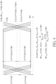
- FIG. 3 shows data signals without the voltage level adjustment mechanism and data signals with the voltage level adjustment mechanism according to one embodiment of the present invention.
- the memory interface circuit 112 does not have the voltage level adjustment mechanism (i.e., the pull-up variable resistor R WPU [1] - R WPU[ 8] and/or the pull-down variable resister R WPD [1] - R WPD [8] do not appear in FIG. 2 )
- the reference voltage VREF may not be suitable for determining a logical value of each data signal.
- the middle voltage level of the data signal DQ1 is lower than the reference voltage VREF
- the middle voltage level of the data signal DQ2 is higher than the reference voltage VREF
- the middle voltage level of the data signal DQ1 is lower than the reference voltage VREF
- the middle voltage level of the data signal DQ1 is equal to the reference voltage VREF.
- every data signal DQ1 - DQ8 has the middle voltage level that is equal to or very close to the reference voltage VREF, so that the reference voltage VREF is suitable for determining logical values of each of the data signals DQ1 - DQ8.
- the pull-up variable resistors R WPU [1] - R WPU[ 8] are weakly-pull-high resistors
- the pull-down variable resistors R WPD [1] - R WPD [8] are weakly-pull-high resistors. Therefore, each of the pull-up variable resistors R WPU [1] - R WPU[ 8] and pull-down variable resistors R WPD [1] - R WPD [8] has higher resistance.
- the memory interface circuit 122 of the DRAM module 120 has on-die termination resistors R ODT [1] - R ODT [8] for improving the impedance mismatch in transmission lines, wherein the on-die termination resistors R ODT [1] - R ODT [8] are positioned at the input terminals of the receivers 222_1 - 222_8, respectively.
- the resistance of each of pull-up variable resistors R WPU [1] - R WPU [8] and pull-down variable resistors R WPD [1] - R WPD [8] is much higher than the resistance of each of the on-die termination resistors R ODT [1] - R ODT [8], for example, the resistance of the variable resistor R WPU [1]/R WPD [1] is several hundred times the resistance of the on-die termination resistor R ODT [1].
- FIG. 4 shows an adjustment of the middle voltage level of the data signal DQ (e.g. each of DQ1 - DQ8) according to one embodiment of the present invention, wherein the symbol R ODT can be used to represent each of the on-die termination resistors R ODT [1] - R ODT [8], the symbol R WPU can be used to represent each of the pull-up variable resistors R WPU [1] - R WPU [8], and the symbol R OP /R ON is used to represent the output impedance of each of the transmitters 212_1 - 212_8.
- the symbol R ODT can be used to represent each of the on-die termination resistors R ODT [1] - R ODT [8]
- the symbol R WPU can be used to represent each of the pull-up variable resistors R WPU [1] - R WPU [8]
- the symbol R OP /R ON is used to represent the output impedance of each of the transmitters 212_1 - 212_
- the middle voltage level V1 of the data signal DQ is equal to 0.5*VOH
- the output impedance R OP /R ON of the transmitter and the resistance of the on-die termination resistor ODT is equal to 'R'
- the resistance of the pull-up variable resistor R WPU is much greater than 'R'.
- FIG. 5 shows an adjustment of the middle voltage level of the data signal DQ (e.g. each of DQ1 - DQ8) according to one embodiment of the present invention, wherein the symbol R ODT can be used to represent each of the on-die termination resistors R ODT [1] - R ODT [8], the symbol R WPD can be used to represent each of the pull-down variable resistors R WPD [1] - R WPD [8], and the symbol R OP /R ON is used to represent the output impedance of each of the transmitters 212_1 - 212_8.
- the symbol R ODT can be used to represent each of the on-die termination resistors R ODT [1] - R ODT [8]
- the symbol R WPD can be used to represent each of the pull-down variable resistors R WPD [1] - R WPD [8]
- the symbol R OP /R ON is used to represent the output impedance of each of the transmitters 212_1 - 212_
- the middle voltage level V1 of the data signal DQ is equal to 0.5*VOH
- the output impedance R OP /R ON of the transmitter and the resistance of the on-die termination resistor R ODT is equal to 'R'
- the resistance of the pull-up variable resistor R WPU is much greater than 'R'.
- FIG. 4 shows the relationship between the pull-up variable resistor R WPU and the middle voltage level of the data signal DQ
- FIG. 5 shows the relationship between the pull-down variable resistor R WPD and the middle voltage level of the data signal DQ
- the control circuit 114 can determine the suitable middle voltage level of the data signal DQ by controlling the resistance of the variable resistors R WPU and R WPD .
- a look-up table may be built in a test stage of the memory system 100, and the control circuit 114 may refer to the reference voltage REF and the look-up table to determine the appropriate resistance of the variable resistors R WPU and R WPD .
- FIG. 6 is diagram illustrating a transmitter and related circuits according to one embodiment of the present invention, wherein the transmitter 212_1 shown in FIG. 2 is used as an example, but the structure shown in FIG. 6 can be applied to any one of the transmitters 212_1 - 212_8. As shown in FIG.
- the transmitter 212_1 comprises transistors M1 - M4 and two resistors R1 and R2, wherein a drain electrode of the transistor M1 is coupled to the supply voltage VDD_TX, a drain electrode of the transistor M2 is coupled to a source electrode of the transistor M1, and a source electrode of the transistor M2 is coupled to an output terminal N1 via the resistor R1; and a source electrode of the transistor M4 is coupled to the ground voltage, a source electrode of the transistor M3 is coupled to a drain electrode of the transistor M3, and a drain electrode of the transistor M3 is coupled to the output terminal N1 via the resistor R2.
- the transistors M1 and M4 are controlled by a driver enable signal DRV_EN, wherein the driver enable signal DRV_EN is configured to enable the transistors M1 and M4 to allow the transmitter 212_1 to transmit the data signal, and to disable the transistors M1 and M4 to make the transmitter 212_1 be unable to transmit the data signal.
- the driver enable signal DRV_EN is configured to enable the transistors M1 and M4 to allow the transmitter 212_1 to transmit the data signal, and to disable the transistors M1 and M4 to make the transmitter 212_1 be unable to transmit the data signal.
- the transistors M2 and M3 are controlled by a pull-up signal DATA_PU[1] and a pull-down signal DATA_PD[1], respectively, wherein the transmitter 212_1 will output the data signal with a higher voltage level if the transistor M2 is enabled while the transistor M3 is disabled; and the transmitter 212_1 will output the data signal with a lower voltage level if the transistor M2 is disabled while the transistor M3 is enabled.
- FIG. 6 further comprises transistors M5-M8 and multiplexers 610 and 620, wherein a source electrode of the transistor M5 is coupled to the supply voltage VDD_TX, a source electrode of the transistor M6 is coupled to a drain electrode of the transistor M5, and a drain electrode of the transistor M6 is coupled to the output terminal N1 via the pull-up variable resistor R WPU [1]; and a source electrode of the transistor M8 is coupled to the ground voltage, a source electrode of the transistor M7 is coupled to a drain electrode of the transistor M8, and a drain electrode of the transistor M7 is coupled to the output terminal N1 via the pull-down variable resistor R WPD [1].
- the transistors M5 and M6 serve as a switching circuit to selectively connect the supply voltage VDD_TX to the pull-up variable resistor R WPU [1], and the transistors M7 and M8 serve as another switching circuit to selectively connect the ground voltage to the pull-down variable resistor R WPD [1].
- the multiplexer 610 receives a dynamic mode pull-up signal DATA_WPU[1] and a static mode pull-up signal OE_WPU[1], and selects one of the dynamic mode pull-up signal DATA_WPU[1] and the static mode pull-up signal OE_WPU[1] to generate a first multiplexer signal according to a selection signal SEL, to control the transistors M5 and M6; and the multiplexer 620 receives a dynamic mode pull-down signal DATA_WPD[1] and a static mode pull-down signal OE_WPD[1], and selects one of the dynamic mode pull-down signal DATA_WPD[1] and the static mode pull-down signal OE_WPD[1] to generate a second multiplexer signal according to the selection signal SEL, to control the transistors M7 and M8.
- the static mode means that the transistors M5 - M8 are always enabled if the transmitter 212_1 is allowed to transmit the data signal DQ1 (e.g., when an output enable (OE) signal of the DRAM interface is on), and the dynamic mode means that the transistors M5 - M8 are enabled only when the transmitter 212_1 transmits the data signal DQ1, that is the transistors M5 - M8 are controlled to be enabled or disabled bit-by-bit, wherein the dynamic mode can lower the power consumption.
- OE output enable
- all the transmitters 212_1 - 212_8 have the voltage level adjustment mechanism to adjust the voltage levels of the data signals DQ1 - DQ8, respectively.
- the present invention is not limited to this. In other embodiments, only part of the transmitters 212_1 - 212_8 have the voltage level adjustment mechanism, and the voltage levels of the data signals outputted by the other transmitters are not controlled according to the reference voltage VREF of the DRAM module 120. This alternative design shall fall within the scope of the present invention.
- each transmitter can be controlled to output data signal with an appropriate voltage level, so that the receivers of the memory module can use the same reference voltage to accurately determine the logical values of the data signals. Therefore, the voltage level adjustment mechanism of the DRAM controller can improve the performance of the receivers in the DRAM module.
- the present invention may also be defined by means of the following numbered clauses.
Landscapes
- Engineering & Computer Science (AREA)
- Computer Hardware Design (AREA)
- Microelectronics & Electronic Packaging (AREA)
- General Engineering & Computer Science (AREA)
- Theoretical Computer Science (AREA)
- Physics & Mathematics (AREA)
- General Physics & Mathematics (AREA)
- Dram (AREA)
- Debugging And Monitoring (AREA)
Abstract
Description
- This application claims the priority of
US Provisional Application No. 63/053,763 (filed on July 20th, 2020 US Provisional Application No. 63/092,530 (filed on October 16th, 2020 - In a dynamic random access memory (DRAM) system, there are a plurality of channels between a DRAM controller and a DRAM module, for transmissions of data signals (i.e., DQ signal). Each channel can be used for bi-directional data transmission, that is the DRAM controller has a transmitter and a receiver for each channel, and the DRAM module also has a transmitter and a receiver for each channel. When the DRAM controller transmits DQ signals to the DRAM module via the plurality of channels, receivers of the DRAM module can use a reference voltage to determine logical values (i.e., bits) of the DQ signals. For example, if a receiver determines that a voltage level of the DQ signal is higher than the reference voltage, the receiver can determine that the DQ signal has a logical value '1'; and if the receiver determines that the voltage level of the DQ signal is lower than the reference voltage, the receiver can determine that the DQ signal has a logical value '0'. Ideally, the reference voltage used by the receivers should be an average of highest voltage level and a lowest voltage level of the DQ signal. However, due to the channel mismatch and semiconductor process variation, the voltage levels of the plurality of channels may be different, that is the single reference voltage is not suitable for every receiver. Furthermore, near-ground signaling (NGS) is widely adopted in modern low-power DRAM interface, and the DQ signals using the NGS technology generally have lower swing and higher speed. Therefore, if the reference voltage is not suitable for some receivers, the misjudgment of logical values will become more serious.
- It is therefore an objective of the present invention to provide a memory controller having a plurality of transmitter, wherein each transmitter can be controlled to output data signal with an appropriate voltage level, so that the receivers of the memory module can use the same reference voltage to accurately determine the logical values of the data signals, to solve the above-mentioned problems.
- According to one embodiment of the present invention, a memory controller comprises a plurality of channels is disclosed. A first channel of the plurality of channels comprises a first transmitter, a first pull-up variable resistor and a first pull-down variable resistor, wherein the first transmitter is configured to generate a first data signal to a memory module, the first pull-up variable resistor is coupled between a supply voltage and an output terminal of the first transmitter, and the first pull-down variable resistor is coupled to the output terminal of the first transmitter. The control circuit is coupled to the plurality of channels, and is configured to control the first pull-up variable resistor and/or the first pull-down variable resistor according to a reference voltage used by the memory module.
- According to another embodiment of the present invention, a memory system comprising a memory controller and a memory module is disclosed. The memory controller comprises a plurality of transmitters, wherein the transmitters are configured to generate a plurality of data signals, respectively; and the memory module comprises a plurality of receivers, wherein the receivers compare the plurality of data signals with a reference voltage to generate a plurality of output signals, respectively. The plurality of transmitters comprise a first transmitter, the memory controller further comprises a first pull-up variable resistor and a first pull-down variable resistor, wherein the first pull-up variable resistor is coupled between a supply voltage and an output terminal of the first transmitter, and the first pull-down variable resistor is coupled to the output terminal of the first transmitter; and the memory controller further comprises a control circuit configured to control the first pull-up variable resistor and/or the first pull-down variable resistor according to the reference voltage used by the memory module.
- According to another embodiment of the present invention, a control method of a memory controller is disclosed, wherein the memory controller comprises a plurality of channels. A first channel of the plurality of channels comprises a first transmitter, a first pull-up variable resistor and a first pull-down variable resistor, wherein the first pull-up variable resistor is coupled between a supply voltage and an output terminal of the first transmitter, and the first pull-down variable resistor is coupled to the output terminal of the first transmitter. The control method comprises the steps of: controlling the first pull-up variable resistor and/or the first pull-down variable resistor according to a reference voltage used by the memory module.
- These and other objectives of the present invention will no doubt become obvious to those of ordinary skill in the art after reading the following detailed description of the preferred embodiment that is illustrated in the various figures and drawings.
-
-
FIG. 1 is a diagram illustrating a memory system according to one embodiment of the present invention. -
FIG. 2 shows some transmitters within the memory interface circuit of DRAM controller and some receivers within the memory interface circuit of DRAM module according to one embodiment of the present invention. -
FIG. 3 shows data signals without the voltage level adjustment mechanism and data signals with the voltage level adjustment mechanism according to one embodiment of the present invention. -
FIG. 4 shows an adjustment of the middle voltage level of the data signal DQ according to one embodiment of the present invention -
FIG. 5 shows an adjustment of the middle voltage level of the data signal DQ according to one embodiment of the present invention -
FIG. 6 is diagram illustrating a transmitter and related circuits according to one embodiment of the present invention. -
FIG. 1 is a diagram illustrating amemory system 100 according to one embodiment of the present invention. As shown inFIG. 1 , thememory system 100 comprises a memory controller (in this embodiment, aDRAM controller 110 serve as the memory controller) and a memory module (in this embodiment, aDRAM module 120 serves as the memory module), where theDRAM controller 110 comprises amemory interface circuit 112 and acontrol circuit 114, and theDRAM module 120 comprises amemory interface circuit 122, acontrol circuit 124 and amemory array 126. In this embodiment, theDRAM controller 110 and theDRAM module 120 are connected via a plurality of connection lines, where the connection lines are used to transmit at least a plurality of a bi-directional data signal DQ, a bi-directional data strobe signal DQS, a plurality of command signals CMDs, a differential clock signal CLK. - When the
memory system 100 is implemented by a DRAM system, the command signals may comprise at least a row address strobe, a column address strobe, and a write enable signal. In addition, the clock signal or the command signals shown inFIG. 1 can be single-directional or bi-directional. - In the general operations of the
memory system 100, theDRAM controller 110 is arranged to receive a request from a host or a processor, and to transmit at least a portion of the data signal DQ, data strobe signal DQS, command signals CMDs, the clock signal CLK and the clock enable signal CKE to access theDRAM module 120. In addition, thecontrol circuit 114 within theDRAM controller 110 may comprise associated circuits, such as a processing circuit, a write/read buffer, a control logic and an arbiter, to perform the related operations. Thememory interface circuit 112 of theDRAM controller 110 is arranged to output the data signal DQ, data strobe signal DQS, command signals CMDs, the clock signal CLK to theDRAM module 120. Thememory interface circuit 122 is arranged to receive the data signal DQ, data strobe signal DQS, command signals CMDs and the clock signal CLK from theDRAM controller 110, and to output the data to theDRAM controller 110 via the DQ connection lines. Thecontrol circuit 124 may comprise a read/write controller, a row decoder and a column decoder, and thecontrol circuit 124 is arranged to receive output signals from thememory interface circuit 122 to access thememory array 126. -
FIG. 2 shows some transmitters 212_1 - 212_8 within thememory interface circuit 112 and some receivers 222_1 - 222_8 within thememory interface circuit 122 according to one embodiment of the present invention. In this embodiment,FIG. 2 shows eight channels between theDRAM controller 110 and theDRAM module 120, and the eight channels are configured to transmit the data signals DQ. Regarding a first channel shown inFIG. 2 , the transmitter 212_1 is coupled between a supply voltage VDD_TX and a reference voltage (e.g. a ground voltage), and the receiver 222_1 is coupled between a supply voltage VDD_RX and the reference voltage (e.g. the ground voltage); and the transmitter 212_1 is configured to receive and output a data signal DQ1 to the receiver 222_1, and the receiver 222_1 compares the data signal DQ1 with a reference voltage VREF to generate an output signal Vout1 , wherein if the data signal DQ1 is greater than the reference voltage VREF, the output signal Vout1 has a higher level indicating that the data signal DQ1 has a logical value '1'; and if the data signal DQ1 is lower than the reference voltage VREF, the output signal Vout1 has a lower level indicating that the data signal DQ1 has a logical value '0'. Similarly, works of the other channels are similar to the work of the first channel. For example, the transmitter 212_8 is coupled between the supply voltage VDD_TX and the ground voltage, and the receiver 222_8 is coupled between a supply voltage VDD_RX and the ground voltage; and the transmitter 212_8 is configured to receive and output a data signal DQ8 to the receiver 222_8, and the receiver 222_8 compares the data signal DQ8 with the reference voltage VREF to generate the output signal, wherein if the data signal DQ8 is greater than the reference voltage VREF, the output signal Vout8 has a higher level indicating that the data signal DQ8 has a logical value '1'; and if the data signal DQ8 is lower than the reference voltage VREF, the output signal Vout8 has a lower level indicating that the data signal DQ8 has a logical value '0'. - As described in the background, due to the channel mismatch and semiconductor process variation, the voltage levels of the plurality of channels (i.e. the transmitted DQ signals of the transmitters 212_1 - 212_8) may be different, that is the single reference voltage VREF is not suitable for every receiver 222_1 - 222_8. To solve this problem, in the
memory interface circuit 112, each of the transmitters 212_1 - 212_8 has a voltage level adjustment mechanism to adjust a voltage level of the transmitted DQ signal, so that a middle voltage level of each data signal DQ can be as close to the reference voltage VREF as possible, wherein the middle voltage level may be an average of a highest voltage level and a lowest voltage level of the data signal DQ. Specifically, taking the first channel as an example, a pull-up variable resistor RWPU[1] is coupled between the supply voltage VDD_TX and an output terminal of the transmitter 212_1, and a pull-down variable resister RWPD[1] is coupled between the ground voltage and the output terminal of the transmitter 212_1. In one embodiment, in the operations of thememory system 100, theDRAM module 120 may calibrate the reference voltage VREF based on training signals to determine an appropriate level for the reference voltage VREF, and theDRAM module 120 can feedback the information of the reference voltage VREF to theDRAM controller 110, so that thecontrol circuit 114 can control the pull-up variable resistor RWPU[1] and/or the pull-down variable resister RWPD[1] to make the middle voltage level of the DQ1 is as close to the reference voltage VREF as possible. In another embodiment, theDRAM module 120 may feedback a bit error rate or a bit error count to theDRAM controller 110, so that thecontrol circuit 114 can control the pull-up variable resistor RWPU[1] and/or the pull-down variable resister RWPD[1] to have the lowest error rate or the bit error count (it also means that the middle voltage level of the DQ1 received by the receiver 222_1 is very close to the reference voltage VREF). - Similarly, voltage level adjustment mechanism of the other channels is similar to the mechanism of the first channel. Taking the eighth channel as an example, a pull-up variable resistor RWPU[8] is coupled between the supply voltage VDD_TX and an output terminal of the transmitter 212_8, and a pull-down variable resister RWPD[8] is coupled between the ground voltage and the output terminal of the transmitter 212_8. In one embodiment, in the operations of the
memory system 100, theDRAM module 120 may calibrate the reference voltage VREF based on the training signals to determine the appropriate level for the reference voltage VREF, and theDRAM module 120 can feedback the information of the reference voltage VREF to theDRAM controller 110, so that thecontrol circuit 114 can control the pull-up variable resistor RWPU[8] and/or the pull-down variable resister RWPD[8] to make the middle voltage level of the DQ8 is as close to the reference voltage VREF as possible. In another embodiment, theDRAM module 120 may feedback a bit error rate or a bit error count to theDRAM controller 110, so that thecontrol circuit 114 can control the pull-up variable resistor RWPU[8] and/or the pull-down variable resister RWPD[8] to have the lowest error rate or the bit error count (it also means that the middle voltage level of the DQ8 received by the receiver 222_8 is very close to the reference voltage VREF). -
FIG. 3 shows data signals without the voltage level adjustment mechanism and data signals with the voltage level adjustment mechanism according to one embodiment of the present invention. Referring to an upper part ofFIG. 3 , if thememory interface circuit 112 does not have the voltage level adjustment mechanism (i.e., the pull-up variable resistor RWPU[1] - RWPU[8] and/or the pull-down variable resister RWPD[1] - RWPD[8] do not appear inFIG. 2 ), the reference voltage VREF may not be suitable for determining a logical value of each data signal. For example, the middle voltage level of the data signal DQ1 is lower than the reference voltage VREF, the middle voltage level of the data signal DQ2 is higher than the reference voltage VREF, the middle voltage level of the data signal DQ1 is lower than the reference voltage VREF, the middle voltage level of the data signal DQ1 is equal to the reference voltage VREF. Referring to a lower part ofFIG. 3 , by controlling the pull-up variable resistor RWPU[1] - RWPU[8] and/or the pull-down variable resister RWPD[1] - RWPD[8] of the channels, every data signal DQ1 - DQ8 has the middle voltage level that is equal to or very close to the reference voltage VREF, so that the reference voltage VREF is suitable for determining logical values of each of the data signals DQ1 - DQ8. - In the embodiment shown in
FIG. 2 , the pull-up variable resistors RWPU[1] - RWPU[8] are weakly-pull-high resistors, and the pull-down variable resistors RWPD[1] - RWPD[8] are weakly-pull-high resistors. Therefore, each of the pull-up variable resistors RWPU[1] - RWPU[8] and pull-down variable resistors RWPD[1] - RWPD[8] has higher resistance. In addition, thememory interface circuit 122 of theDRAM module 120 has on-die termination resistors RODT[1] - RODT[8] for improving the impedance mismatch in transmission lines, wherein the on-die termination resistors RODT[1] - RODT[8] are positioned at the input terminals of the receivers 222_1 - 222_8, respectively. In this embodiment, the resistance of each of pull-up variable resistors RWPU[1] - RWPU[8] and pull-down variable resistors RWPD[1] - RWPD[8] is much higher than the resistance of each of the on-die termination resistors RODT[1] - RODT[8], for example, the resistance of the variable resistor RWPU[1]/RWPD[1] is several hundred times the resistance of the on-die termination resistor RODT[1]. -
FIG. 4 shows an adjustment of the middle voltage level of the data signal DQ (e.g. each of DQ1 - DQ8) according to one embodiment of the present invention, wherein the symbol RODT can be used to represent each of the on-die termination resistors RODT[1] - RODT[8], the symbol RWPU can be used to represent each of the pull-up variable resistors RWPU[1] - RWPU[8], and the symbol ROP/RON is used to represent the output impedance of each of the transmitters 212_1 - 212_8. As shown inFIG. 4 , assuming that the data signal DQ initially has a highest voltage level VOH and a lowest voltage level 0V, the middle voltage level V1 of the data signal DQ is equal to 0.5*VOH, the output impedance ROP/RON of the transmitter and the resistance of the on-die termination resistor ODT is equal to 'R', and the resistance of the pull-up variable resistor RWPU is much greater than 'R'. Thecontrol circuit 114 can control the resistance of the pull-up variable resistor RWPU to increase the lowest voltage level and the highest voltage level of the data signal DQ, and the equations showing an increase of lowest voltage level and an increase of highest voltage level are as follows:

control circuit 114 can determine that the middle voltage level V1' of the data signal DQ becomes (0.5*VOH+1.5* ΔV). -
FIG. 5 shows an adjustment of the middle voltage level of the data signal DQ (e.g. each of DQ1 - DQ8) according to one embodiment of the present invention, wherein the symbol RODT can be used to represent each of the on-die termination resistors RODT[1] - RODT[8], the symbol RWPD can be used to represent each of the pull-down variable resistors RWPD[1] - RWPD[8], and the symbol ROP/RON is used to represent the output impedance of each of the transmitters 212_1 - 212_8. As shown inFIG. 5 , assuming that the data signal DQ initially has a highest voltage level VOH and a lowest voltage level 0V, the middle voltage level V1 of the data signal DQ is equal to 0.5*VOH, the output impedance ROP/RON of the transmitter and the resistance of the on-die termination resistor RODT is equal to 'R', and the resistance of the pull-up variable resistor RWPU is much greater than 'R'. Thecontrol circuit 114 can control the resistance of the pull-down variable resistor RWPD to decrease the highest voltage level of the data signal DQ, and the equations showing a decrease of highest voltage level are as follows:
control circuit 114 can determine that the middle voltage level V1' of the data signal DQ becomes (0.5*VOH-ΔV). -
FIG. 4 shows the relationship between the pull-up variable resistor RWPU and the middle voltage level of the data signal DQ, andFIG. 5 shows the relationship between the pull-down variable resistor RWPD and the middle voltage level of the data signal DQ, therefore, thecontrol circuit 114 can determine the suitable middle voltage level of the data signal DQ by controlling the resistance of the variable resistors RWPU and RWPD. - It is noted that the embodiments shown in
FIG. 4 andFIG. 5 are for illustrative purposes only. In other embodiments, a look-up table may be built in a test stage of thememory system 100, and thecontrol circuit 114 may refer to the reference voltage REF and the look-up table to determine the appropriate resistance of the variable resistors RWPU and RWPD. -
FIG. 6 is diagram illustrating a transmitter and related circuits according to one embodiment of the present invention, wherein the transmitter 212_1 shown inFIG. 2 is used as an example, but the structure shown inFIG. 6 can be applied to any one of the transmitters 212_1 - 212_8. As shown inFIG. 6 , the transmitter 212_1 comprises transistors M1 - M4 and two resistors R1 and R2, wherein a drain electrode of the transistor M1 is coupled to the supply voltage VDD_TX, a drain electrode of the transistor M2 is coupled to a source electrode of the transistor M1, and a source electrode of the transistor M2 is coupled to an output terminal N1 via the resistor R1; and a source electrode of the transistor M4 is coupled to the ground voltage, a source electrode of the transistor M3 is coupled to a drain electrode of the transistor M3, and a drain electrode of the transistor M3 is coupled to the output terminal N1 via the resistor R2. The transistors M1 and M4 are controlled by a driver enable signal DRV_EN, wherein the driver enable signal DRV_EN is configured to enable the transistors M1 and M4 to allow the transmitter 212_1 to transmit the data signal, and to disable the transistors M1 and M4 to make the transmitter 212_1 be unable to transmit the data signal. The transistors M2 and M3 are controlled by a pull-up signal DATA_PU[1] and a pull-down signal DATA_PD[1], respectively, wherein the transmitter 212_1 will output the data signal with a higher voltage level if the transistor M2 is enabled while the transistor M3 is disabled; and the transmitter 212_1 will output the data signal with a lower voltage level if the transistor M2 is disabled while the transistor M3 is enabled. - In addition,
FIG. 6 further comprises transistors M5-M8 andmultiplexers multiplexer 610 receives a dynamic mode pull-up signal DATA_WPU[1] and a static mode pull-up signal OE_WPU[1], and selects one of the dynamic mode pull-up signal DATA_WPU[1] and the static mode pull-up signal OE_WPU[1] to generate a first multiplexer signal according to a selection signal SEL, to control the transistors M5 and M6; and themultiplexer 620 receives a dynamic mode pull-down signal DATA_WPD[1] and a static mode pull-down signal OE_WPD[1], and selects one of the dynamic mode pull-down signal DATA_WPD[1] and the static mode pull-down signal OE_WPD[1] to generate a second multiplexer signal according to the selection signal SEL, to control the transistors M7 and M8. In this embodiment, the static mode means that the transistors M5 - M8 are always enabled if the transmitter 212_1 is allowed to transmit the data signal DQ1 (e.g., when an output enable (OE) signal of the DRAM interface is on), and the dynamic mode means that the transistors M5 - M8 are enabled only when the transmitter 212_1 transmits the data signal DQ1, that is the transistors M5 - M8 are controlled to be enabled or disabled bit-by-bit, wherein the dynamic mode can lower the power consumption. - In the above embodiments, all the transmitters 212_1 - 212_8 have the voltage level adjustment mechanism to adjust the voltage levels of the data signals DQ1 - DQ8, respectively. However, the present invention is not limited to this. In other embodiments, only part of the transmitters 212_1 - 212_8 have the voltage level adjustment mechanism, and the voltage levels of the data signals outputted by the other transmitters are not controlled according to the reference voltage VREF of the
DRAM module 120. This alternative design shall fall within the scope of the present invention. - Briefly summarized, in the DRAM controller of the present invention, each transmitter can be controlled to output data signal with an appropriate voltage level, so that the receivers of the memory module can use the same reference voltage to accurately determine the logical values of the data signals. Therefore, the voltage level adjustment mechanism of the DRAM controller can improve the performance of the receivers in the DRAM module.
- Those skilled in the art will readily observe that numerous modifications and alterations of the device and method may be made while retaining the teachings of the invention. Accordingly, the above disclosure should be construed as limited only by the metes and bounds of the appended claims.
- The present invention may also be defined by means of the following numbered clauses.
- 1. A memory controller, comprising:
a plurality of channels, wherein a first channel of the plurality of channels comprises:- a first transmitter, configured to generate a first data signal to a memory module;
- a first pull-up variable resistor, coupled between a supply voltage and an output terminal of the first transmitter; and
- a first pull-down variable resistor, coupled to the output terminal of the first transmitter; and
- a control circuit, coupled to the plurality of channels, configured to control the first pull-up variable resistor and/or the first pull-down variable resistor according to a reference voltage used by the memory module.
- 2. The memory controller of
clause 1, wherein the control circuit is configured to control the first pull-up variable resistor and/or the first pull-down variable resistor to make a middle voltage level of the first data signal outputted by the first transmitter is substantially equal to the reference voltage used by the memory module. - 3. The memory controller of
clause 1, wherein a second channel of the plurality of channels comprises:- a second transmitter, configured to generate a second data signal to the memory module;
- a second pull-up variable resistor, coupled between the supply voltage and an output terminal of the second transmitter; and
- a second pull-down variable resistor, coupled to the output terminal of the second transmitter; and
- wherein the control circuit is further configured to control the second pull-up variable resistor and/or the second pull-down variable resistor according to the reference voltage used by the memory module.
- 4. The memory controller of clause 3, wherein the control circuit is configured to control the second pull-up variable resistor and/or the second pull-down variable resistor to make a middle voltage level of the second data signal outputted by the second transmitter is substantially equal to the reference voltage used by the memory module.
- 5. The memory controller of clause 4, wherein the control circuits separately controls the first pull-up/pull-down variable resistor and the second pull-up/pull-down variable resistor so that the middle voltage level of the second data signal is not equal to a middle voltage level of the first data signal.
- 6. The memory controller of
clause 1, wherein the first channel further comprises:
a first switching circuit, coupled between the first pull-up variable resistor and the supply voltage, configured to connect the supply voltage to the first pull-up variable resistor or disconnect the first pull-up variable resistor from the supply voltage. - 7. The memory controller of clause 6, wherein the first switching is controlled by a static mode pull-up signal so that the first switching is always enabled when the first transmitter is enabled.
- 8. The memory controller of clause 6, wherein the first switching is controlled by a dynamic mode pull-up signal so that the first switching is enabled only when the first transmitter generates the first data signal, and the control circuit enables the first switching bit-by-bit.
- 9. A memory system, comprising:
- a memory controller comprising a plurality of transmitters, wherein the transmitters are configured to generate a plurality of data signals, respectively; and
- a memory module comprising a plurality of receivers, wherein the receivers compare the plurality of data signals with a reference voltage to generate a plurality of output signals, respectively;
- wherein the plurality of transmitters comprise a first transmitter, the memory controller further comprises a first pull-up variable resistor and a first pull-down variable resistor, wherein the first pull-up variable resistor is coupled between a supply voltage and an output terminal of the first transmitter, and the first pull-down variable resistor is coupled to the output terminal of the first transmitter; and the memory controller further comprises a control circuit configured to control the first pull-up variable resistor and/or the first pull-down variable resistor according to the reference voltage used by the memory module.
- 10. The memory system of clause 9, wherein the control circuit is configured to control the first pull-up variable resistor and/or the first pull-down variable resistor to make a middle voltage level of a first data signal outputted by the first transmitter is substantially equal to the reference voltage used by the memory module.
- 11. The memory system of clause 9, wherein the plurality of transmitters comprise a second transmitter, the memory controller further comprises a second pull-up variable resistor and a second pull-down variable resistor, wherein the second pull-up variable resistor is coupled between the supply voltage and an output terminal of the second transmitter, and the second pull-down variable resistor is coupled to the output terminal of the second transmitter; and the control circuit is further configured to control the second pull-up variable resistor and/or the second pull-down variable resistor according to the reference voltage used by the memory module.
- 12. The memory system of clause 11, wherein the control circuit is configured to control the second pull-up variable resistor and/or the second pull-down variable resistor to make a middle voltage level of a second data signal outputted by the second transmitter is substantially equal to the reference voltage used by the memory module.
- 13. The memory system of clause 12, wherein the control circuits separately controls the first pull-up/pull-down variable resistor and the second pull-up/pull-down variable resistor so that the middle voltage level of the second data signal is not equal to a middle voltage level of the first data signal.
- 14. A control method of a memory controller, wherein the memory controller comprises a plurality of channels, and a first channel of the plurality of channels comprises:
- a first transmitter;
- a first pull-up variable resistor, coupled between a supply voltage and an output terminal of the first transmitter; and
- a first pull-down variable resistor, coupled to the output terminal of the first transmitter; and
- the control method comprises the steps of:
controlling the first pull-up variable resistor and/or the first pull-down variable resistor according to a reference voltage used by the memory module.
- 15. The control method of clause 14, wherein the step of controlling the first pull-up variable resistor and/or the first pull-down variable resistor according to the reference voltage used by the memory module comprises:
controlling the first pull-up variable resistor and/or the first pull-down variable resistor to make a middle voltage level of a first data signal outputted by the first transmitter is substantially equal to the reference voltage used by the memory module. - 16. The control method of clause 14, wherein a second channel of the plurality of channels comprises:
- a second transmitter;
- a second pull-up variable resistor, coupled between the supply voltage and an output terminal of the second transmitter; and
- a second pull-down variable resistor, coupled to the output terminal of the second transmitter; and
- the control method further comprises:
controlling the second pull-up variable resistor and/or the second pull-down variable resistor according to the reference voltage used by the memory module.
- 17. The control method of clause 16, wherein the step of controlling the second pull-up variable resistor and/or the second pull-down variable resistor according to the reference voltage used by the memory module comprises:
controlling the second pull-up variable resistor and/or the second pull-down variable resistor to make a middle voltage level of the second data signal outputted by the second transmitter is substantially equal to the reference voltage used by the memory module. - 18. The control method of clause 17, wherein the first pull-up/pull-down variable resistor and the second pull-up/pull-down variable resistor are separately controlled so that the middle voltage level of the second data signal is not equal to a middle voltage level of the first data signal.
Claims (15)
- A memory controller (110), comprising:a plurality of channels, wherein a first channel of the plurality of channels comprises:a first transmitter (222_1), configured to generate a first data signal to a memory module (120);a first pull-up variable resistor (RWPU[1]), coupled between a supply voltage and an output terminal of the first transmitter (222_1); anda first pull-down variable resistor (RWPD[1), coupled to the output terminal of the first transmitter(222_1); anda control circuit (114), coupled to the plurality of channels, configured to control the first pull-up variable resistor (RWPU[1]) and/or the first pull-down (RWPD[1]) variable resistor according to a reference voltage used by the memory module (120).
- The memory controller (110) of claim 1, wherein the control circuit (114) is configured to control the first pull-up variable resistor (RWPU[1]) and/or the first pull-down variable resistor (RWPD[1]) to make a middle voltage level of the first data signal outputted by the first transmitter (222_1) is substantially equal to the reference voltage used by the memory module (120).
- The memory controller (110) of claim 1, wherein a second channel of the plurality of channels comprises:a second transmitter (221_8), configured to generate a second data signal to the memory module (120);a second pull-up variable resistor (RWPU[8]) , coupled between the supply voltage and an output terminal of the second transmitter (221_8); anda second pull-down variable resistor (RWPD[8]) , coupled to the output terminal of the second transmitter (221_8); andwherein the control circuit (114) is further configured to control the second pull-up variable resistor (RWPU[8]) and/or the second pull-down variable resistor (RWPD[8]) according to the reference voltage used by the memory module (120).
- The memory controller (110) of claim 3, wherein the control circuit (114) is configured to control the second pull-up variable resistor (RWPU[8]) and/or the second pull-down variable resistor (RWPD[8]) to make a middle voltage level of the second data signal outputted by the second transmitter (221_8) is substantially equal to the reference voltage used by the memory module (120).
- The memory controller (110) of claim 4, wherein the control circuits (114) separately controls the first pull-up/pull-down variable resistor and the second pull-up/pull-down variable resistor so that the middle voltage level of the second data signal is not equal to a middle voltage level of the first data signal.
- The memory controller (110) of claim 1, wherein the first channel further comprises:
a first switching circuit, coupled between the first pull-up variable resistor (RWPU[1]) and the supply voltage, configured to connect the supply voltage to the first pull-up variable resistor (RWPU[1]) or disconnect the first pull-up variable resistor (RWPU[1]) from the supply voltage. - The memory controller (110) of claim 6, wherein the first switching is controlled by a static mode pull-up signal so that the first switching is always enabled when the first transmitter (222_1) is enabled; or
wherein the first switching is controlled by a dynamic mode pull-up signal so that the first switching is enabled only when the first transmitter (222_1) generates the first data signal, and the control circuit (114) enables the first switching bit-by-bit. - A memory system (100), comprising:a memory controller (100) comprising a plurality of transmitters, wherein the transmitters are configured to generate a plurality of data signals, respectively; anda memory module (120) comprising a plurality of receivers, wherein the receivers compare the plurality of data signals with a reference voltage to generate a plurality of output signals, respectively;wherein the plurality of transmitters comprise a first transmitter (222_1), the memory controller further comprises a first pull-up variable resistor (RWPU[1]) and a first pull-down variable resistor (RWPD[1]), wherein the first pull-up variable resistor (RWPU[1]) is coupled between a supply voltage and an output terminal of the first transmitter (222_1), and the first pull-down variable resistor (RWPD[1]) is coupled to the output terminal of the first transmitter (222_1); and the memory controller (110) further comprises a control circuit (114) configured to control the first pull-up variable resistor (RWPU[1]) and/or the first pull-down variable resistor according to the reference voltage used by the memory module (120).
- The memory system (100) of claim 8, wherein the control circuit (114) is configured to control the first pull-up variable resistor (RWPU[1]) and/or the first pull-down variable resistor (RWPD[1]) to make a middle voltage level of a first data signal outputted by the first transmitter (222_1) is substantially equal to the reference voltage used by the memory module (120).
- The memory system (100) of claim 8, wherein the plurality of transmitters comprise a second transmitter (221_8), the memory controller (110) further comprises a second pull-up variable resistor (RWPU[8]) and a second pull-down variable resistor (RWPD[8]), wherein the second pull-up variable resistor (RWPU[8]) is coupled between the supply voltage and an output terminal of the second transmitter (221_8), and the second pull-down variable resistor (RWPD[8]) is coupled to the output terminal of the second transmitter (221_8); and the control circuit (114) is further configured to control the second pull-up variable resistor (RWPU[8]) and/or the second pull-down variable resistor (RWPD[8]) according to the reference voltage used by the memory module (120).
- The memory system (100) of claim 10, wherein the control circuit (114) is configured to control the second pull-up variable resistor (RWPU[8]) and/or the second pull-down variable resistor (RWPD[8]) to make a middle voltage level of a second data signal outputted by the second transmitter (221_8) is substantially equal to the reference voltage used by the memory module (120).
- The memory system (100) of claim 11, wherein the control circuits (114) separately controls the first pull-up/pull-down variable resistor and the second pull-up/pull-down variable resistor so that the middle voltage level of the second data signal is not equal to a middle voltage level of the first data signal.
- A control method of a memory controller (110), wherein the memory controller (110) comprises a plurality of channels, and a first channel of the plurality of channels comprises:a first transmitter (222_1);a first pull-up variable resistor (RWPU[1]), coupled between a supply voltage and an output terminal of the first transmitter (222_1); anda first pull-down variable resistor (RWPD[1]) , coupled to the output terminal of the first transmitter (222_1); andthe control method comprises the steps of:
controlling the first pull-up variable resistor (RWPU[1]) and/or the first pull-down variable resistor (RWPD[1]) according to a reference voltage used by the memory module (120). - The control method of claim 13, wherein the step of controlling the first pull-up variable resistor (RWPU[1]) and/or the first pull-down variable resistor (RWPD[1]) according to the reference voltage used by the memory module (120) comprises:
controlling the first pull-up variable resistor (RWPU[1]) and/or the first pull-down variable resistor (RWPD[1]) to make a middle voltage level of a first data signal outputted by the first transmitter (222_1) is substantially equal to the reference voltage used by the memory module (120). - The control method of claim 13, wherein a second channel of the plurality of channels comprises:a second transmitter(221_8);a second pull-up variable resistor (RWPU[8]), coupled between the supply voltage and an output terminal of the second transmitter (221_8); anda second pull-down variable resistor (RWPD[8]), coupled to the output terminal of the second transmitter(221_8); andthe control method further comprises:
controlling the second pull-up variable resistor (RWPU[8]) and/or the second pull-down (RWPD[8]) variable resistor according to the reference voltage used by the memory module (120).
Applications Claiming Priority (3)
| Application Number | Priority Date | Filing Date | Title |
|---|---|---|---|
| US202063053763P | 2020-07-20 | 2020-07-20 | |
| US202063092530P | 2020-10-16 | 2020-10-16 | |
| US17/349,934 US11790977B2 (en) | 2020-07-20 | 2021-06-17 | Transmitter with voltage level adjustment mechanism in memory controller |
Publications (1)
| Publication Number | Publication Date |
|---|---|
| EP3944089A1 true EP3944089A1 (en) | 2022-01-26 |
Family
ID=79292704
Family Applications (1)
| Application Number | Title | Priority Date | Filing Date |
|---|---|---|---|
| EP21184984.9A Withdrawn EP3944089A1 (en) | 2020-07-20 | 2021-07-12 | Transmitter with voltage level adjustment mechanism in memory controller |
Country Status (4)
| Country | Link |
|---|---|
| US (1) | US11790977B2 (en) |
| EP (1) | EP3944089A1 (en) |
| CN (1) | CN113963733B (en) |
| TW (1) | TWI806098B (en) |
Families Citing this family (5)
| Publication number | Priority date | Publication date | Assignee | Title |
|---|---|---|---|---|
| KR102799335B1 (en) * | 2020-08-21 | 2025-04-23 | 삼성전자주식회사 | An interface circuit and a system including same |
| US11714576B2 (en) * | 2020-10-29 | 2023-08-01 | Micron Technology, Inc. | Memory bus drive defect detection |
| CN113611667B (en) * | 2021-07-02 | 2024-09-10 | 芯盟科技有限公司 | Transistor array and manufacturing method thereof, semiconductor device and manufacturing method thereof |
| US12482516B2 (en) | 2022-08-19 | 2025-11-25 | Changxin Memory Technologies, Inc. | Circuit for receiving data and memory |
| CN117636927A (en) * | 2022-08-19 | 2024-03-01 | 长鑫存储技术有限公司 | A data receiving circuit and memory |
Citations (4)
| Publication number | Priority date | Publication date | Assignee | Title |
|---|---|---|---|---|
| EP3203475A1 (en) * | 2016-02-02 | 2017-08-09 | MediaTek Inc. | Memory interface circuit capable of controlling driving ability and associated control method |
| US20180167055A1 (en) * | 2016-12-09 | 2018-06-14 | Micron Technology, Inc. | Apparatuses and methods for calibrating adjustable impedances of a semiconductor device |
| US20190080745A1 (en) * | 2017-09-11 | 2019-03-14 | SK Hynix Inc. | Memory system |
| US20190296691A1 (en) * | 2018-03-20 | 2019-09-26 | Integrated Device Technology, Inc. | Lower power auto-zeroing receiver incorporating ctle, vga, and dfe |
Family Cites Families (13)
| Publication number | Priority date | Publication date | Assignee | Title |
|---|---|---|---|---|
| US6954392B2 (en) * | 2003-03-28 | 2005-10-11 | Micron Technology, Inc. | Method for reducing power consumption when sensing a resistive memory |
| KR100583090B1 (en) * | 2003-05-30 | 2006-05-23 | 주식회사 하이닉스반도체 | Capacitor Manufacturing Method of Ferroelectric Resistors |
| KR100596977B1 (en) * | 2004-08-20 | 2006-07-05 | 삼성전자주식회사 | A reference voltage generator circuit using both an external reference voltage and an internal reference voltage at the same time and a method of generating a reference voltage using the same |
| KR100670699B1 (en) * | 2004-11-01 | 2007-01-17 | 주식회사 하이닉스반도체 | Semiconductor Memory Device with On Die Termination Circuit |
| US7446558B2 (en) | 2006-09-29 | 2008-11-04 | Mediatek Inc. | High speed IO buffer |
| US7876123B2 (en) | 2007-10-09 | 2011-01-25 | Lsi Corporation | High speed multiple memory interface I/O cell |
| EP2583280A4 (en) * | 2010-06-17 | 2014-06-18 | Rambus Inc | Balanced on-die termination |
| US8598941B2 (en) * | 2011-06-21 | 2013-12-03 | Lsi Corporation | Hybrid impedance compensation in a buffer circuit |
| US8836381B2 (en) * | 2012-06-20 | 2014-09-16 | Mosys, Inc. | Pseudo-supply hybrid driver |
| EP3075118B1 (en) * | 2013-11-27 | 2019-11-20 | Intel Corporation | Autonomously controlling a buffer of a processor |
| US10284198B2 (en) * | 2015-10-02 | 2019-05-07 | Samsung Electronics Co., Ltd. | Memory systems with ZQ global management and methods of operating same |
| JP2019193122A (en) | 2018-04-25 | 2019-10-31 | セイコーエプソン株式会社 | Output buffer circuit, oscillator, electronic apparatus, and mobile body |
| KR102670946B1 (en) * | 2019-09-27 | 2024-05-31 | 에스케이하이닉스 주식회사 | Semiconductor apparatus for generating reference voltage |
-
2021
- 2021-06-17 US US17/349,934 patent/US11790977B2/en active Active
- 2021-07-12 EP EP21184984.9A patent/EP3944089A1/en not_active Withdrawn
- 2021-07-14 CN CN202110796062.8A patent/CN113963733B/en active Active
- 2021-07-15 TW TW110126093A patent/TWI806098B/en active
Patent Citations (4)
| Publication number | Priority date | Publication date | Assignee | Title |
|---|---|---|---|---|
| EP3203475A1 (en) * | 2016-02-02 | 2017-08-09 | MediaTek Inc. | Memory interface circuit capable of controlling driving ability and associated control method |
| US20180167055A1 (en) * | 2016-12-09 | 2018-06-14 | Micron Technology, Inc. | Apparatuses and methods for calibrating adjustable impedances of a semiconductor device |
| US20190080745A1 (en) * | 2017-09-11 | 2019-03-14 | SK Hynix Inc. | Memory system |
| US20190296691A1 (en) * | 2018-03-20 | 2019-09-26 | Integrated Device Technology, Inc. | Lower power auto-zeroing receiver incorporating ctle, vga, and dfe |
Also Published As
| Publication number | Publication date |
|---|---|
| TWI806098B (en) | 2023-06-21 |
| US20220020419A1 (en) | 2022-01-20 |
| CN113963733B (en) | 2025-12-12 |
| CN113963733A (en) | 2022-01-21 |
| US11790977B2 (en) | 2023-10-17 |
| TW202205291A (en) | 2022-02-01 |
Similar Documents
| Publication | Publication Date | Title |
|---|---|---|
| US11790977B2 (en) | Transmitter with voltage level adjustment mechanism in memory controller | |
| KR102850417B1 (en) | Receviver performing reference voltage training and memory system including the same | |
| US10284198B2 (en) | Memory systems with ZQ global management and methods of operating same | |
| EP3965104B1 (en) | Memory devices configured to generate pulse amplitude modulation-based dq signals, memory controllers, and memory systems including the memory devices and the memory controllers | |
| US10366045B2 (en) | Flash controller to provide a value that represents a parameter to a flash memory | |
| US10715364B2 (en) | Uniformity between levels of a multi-level signal | |
| KR100744039B1 (en) | Semiconductor memory device that can adjust impedance of data output driver | |
| US8120381B2 (en) | Impedance adjusting device | |
| KR102835912B1 (en) | Multi-level signal receviver and memory system including the same | |
| KR20220050317A (en) | Method of generating signal for test in memory device using multi-level signaling and memory device performing the same | |
| KR102855061B1 (en) | Multi-level signal receviver and memory system including the same | |
| EP3203475B1 (en) | Memory interface circuit capable of controlling driving ability and associated control method | |
| US6760857B1 (en) | System having both externally and internally generated clock signals being asserted on the same clock pin in normal and test modes of operation respectively | |
| US7051130B1 (en) | Integrated circuit device that stores a value representative of a drive strength setting | |
| US20060038577A1 (en) | Methods and circuits for generating reference voltage | |
| US11936377B2 (en) | Impedance control for input/output circuits | |
| KR20170040719A (en) | Memory system with zq global managing scheme | |
| KR100327344B1 (en) | Data output circuit for controlling a slewing rate of output data in semiconductor memory device |
Legal Events
| Date | Code | Title | Description |
|---|---|---|---|
| PUAI | Public reference made under article 153(3) epc to a published international application that has entered the european phase |
Free format text: ORIGINAL CODE: 0009012 |
|
| STAA | Information on the status of an ep patent application or granted ep patent |
Free format text: STATUS: THE APPLICATION HAS BEEN PUBLISHED |
|
| AK | Designated contracting states |
Kind code of ref document: A1 Designated state(s): AL AT BE BG CH CY CZ DE DK EE ES FI FR GB GR HR HU IE IS IT LI LT LU LV MC MK MT NL NO PL PT RO RS SE SI SK SM TR |
|
| STAA | Information on the status of an ep patent application or granted ep patent |
Free format text: STATUS: REQUEST FOR EXAMINATION WAS MADE |
|
| 17P | Request for examination filed |
Effective date: 20220707 |
|
| RBV | Designated contracting states (corrected) |
Designated state(s): AL AT BE BG CH CY CZ DE DK EE ES FI FR GB GR HR HU IE IS IT LI LT LU LV MC MK MT NL NO PL PT RO RS SE SI SK SM TR |
|
| STAA | Information on the status of an ep patent application or granted ep patent |
Free format text: STATUS: EXAMINATION IS IN PROGRESS |
|
| P01 | Opt-out of the competence of the unified patent court (upc) registered |
Effective date: 20230607 |
|
| 17Q | First examination report despatched |
Effective date: 20230703 |
|
| STAA | Information on the status of an ep patent application or granted ep patent |
Free format text: STATUS: THE APPLICATION HAS BEEN WITHDRAWN |
|
| 18W | Application withdrawn |
Effective date: 20231103 |