EP3940942A1 - Power supplies for rf power amplifier - Google Patents
Power supplies for rf power amplifier Download PDFInfo
- Publication number
- EP3940942A1 EP3940942A1 EP21180333.3A EP21180333A EP3940942A1 EP 3940942 A1 EP3940942 A1 EP 3940942A1 EP 21180333 A EP21180333 A EP 21180333A EP 3940942 A1 EP3940942 A1 EP 3940942A1
- Authority
- EP
- European Patent Office
- Prior art keywords
- mode
- power supply
- buck
- type switched
- boost
- Prior art date
- Legal status (The legal status is an assumption and is not a legal conclusion. Google has not performed a legal analysis and makes no representation as to the accuracy of the status listed.)
- Granted
Links
- 238000000034 method Methods 0.000 claims abstract description 59
- 230000005540 biological transmission Effects 0.000 claims abstract description 32
- 230000008030 elimination Effects 0.000 claims abstract description 9
- 238000003379 elimination reaction Methods 0.000 claims abstract description 9
- 238000004891 communication Methods 0.000 claims description 7
- 230000008878 coupling Effects 0.000 claims description 3
- 238000010168 coupling process Methods 0.000 claims description 3
- 238000005859 coupling reaction Methods 0.000 claims description 3
- 238000010586 diagram Methods 0.000 description 8
- 238000004513 sizing Methods 0.000 description 8
- 230000006870 function Effects 0.000 description 6
- 238000005516 engineering process Methods 0.000 description 5
- 238000004590 computer program Methods 0.000 description 4
- 230000007423 decrease Effects 0.000 description 4
- 101100137857 Caenorhabditis elegans pas-4 gene Proteins 0.000 description 3
- 230000001413 cellular effect Effects 0.000 description 3
- 238000010295 mobile communication Methods 0.000 description 3
- WHXSMMKQMYFTQS-UHFFFAOYSA-N Lithium Chemical compound [Li] WHXSMMKQMYFTQS-UHFFFAOYSA-N 0.000 description 2
- 230000003321 amplification Effects 0.000 description 2
- 230000008859 change Effects 0.000 description 2
- 230000006872 improvement Effects 0.000 description 2
- 229910052744 lithium Inorganic materials 0.000 description 2
- 238000004519 manufacturing process Methods 0.000 description 2
- 238000003199 nucleic acid amplification method Methods 0.000 description 2
- 238000012545 processing Methods 0.000 description 2
- 230000004044 response Effects 0.000 description 2
- 238000013459 approach Methods 0.000 description 1
- 238000003491 array Methods 0.000 description 1
- OJIJEKBXJYRIBZ-UHFFFAOYSA-N cadmium nickel Chemical compound [Ni].[Cd] OJIJEKBXJYRIBZ-UHFFFAOYSA-N 0.000 description 1
- 239000003990 capacitor Substances 0.000 description 1
- 230000001419 dependent effect Effects 0.000 description 1
- 238000013461 design Methods 0.000 description 1
- 230000005669 field effect Effects 0.000 description 1
- 238000005259 measurement Methods 0.000 description 1
- 238000012986 modification Methods 0.000 description 1
- 230000004048 modification Effects 0.000 description 1
- 230000003071 parasitic effect Effects 0.000 description 1
Images


Classifications
-
- H—ELECTRICITY
- H03—ELECTRONIC CIRCUITRY
- H03F—AMPLIFIERS
- H03F3/00—Amplifiers with only discharge tubes or only semiconductor devices as amplifying elements
- H03F3/20—Power amplifiers, e.g. Class B amplifiers, Class C amplifiers
- H03F3/21—Power amplifiers, e.g. Class B amplifiers, Class C amplifiers with semiconductor devices only
-
- H—ELECTRICITY
- H02—GENERATION; CONVERSION OR DISTRIBUTION OF ELECTRIC POWER
- H02M—APPARATUS FOR CONVERSION BETWEEN AC AND AC, BETWEEN AC AND DC, OR BETWEEN DC AND DC, AND FOR USE WITH MAINS OR SIMILAR POWER SUPPLY SYSTEMS; CONVERSION OF DC OR AC INPUT POWER INTO SURGE OUTPUT POWER; CONTROL OR REGULATION THEREOF
- H02M3/00—Conversion of dc power input into dc power output
- H02M3/02—Conversion of dc power input into dc power output without intermediate conversion into ac
- H02M3/04—Conversion of dc power input into dc power output without intermediate conversion into ac by static converters
- H02M3/10—Conversion of dc power input into dc power output without intermediate conversion into ac by static converters using discharge tubes with control electrode or semiconductor devices with control electrode
- H02M3/145—Conversion of dc power input into dc power output without intermediate conversion into ac by static converters using discharge tubes with control electrode or semiconductor devices with control electrode using devices of a triode or transistor type requiring continuous application of a control signal
- H02M3/155—Conversion of dc power input into dc power output without intermediate conversion into ac by static converters using discharge tubes with control electrode or semiconductor devices with control electrode using devices of a triode or transistor type requiring continuous application of a control signal using semiconductor devices only
- H02M3/156—Conversion of dc power input into dc power output without intermediate conversion into ac by static converters using discharge tubes with control electrode or semiconductor devices with control electrode using devices of a triode or transistor type requiring continuous application of a control signal using semiconductor devices only with automatic control of output voltage or current, e.g. switching regulators
- H02M3/158—Conversion of dc power input into dc power output without intermediate conversion into ac by static converters using discharge tubes with control electrode or semiconductor devices with control electrode using devices of a triode or transistor type requiring continuous application of a control signal using semiconductor devices only with automatic control of output voltage or current, e.g. switching regulators including plural semiconductor devices as final control devices for a single load
- H02M3/1582—Buck-boost converters
-
- H—ELECTRICITY
- H03—ELECTRONIC CIRCUITRY
- H03F—AMPLIFIERS
- H03F1/00—Details of amplifiers with only discharge tubes, only semiconductor devices or only unspecified devices as amplifying elements
- H03F1/02—Modifications of amplifiers to raise the efficiency, e.g. gliding Class A stages, use of an auxiliary oscillation
- H03F1/0205—Modifications of amplifiers to raise the efficiency, e.g. gliding Class A stages, use of an auxiliary oscillation in transistor amplifiers
- H03F1/0211—Modifications of amplifiers to raise the efficiency, e.g. gliding Class A stages, use of an auxiliary oscillation in transistor amplifiers with control of the supply voltage or current
-
- H—ELECTRICITY
- H02—GENERATION; CONVERSION OR DISTRIBUTION OF ELECTRIC POWER
- H02J—CIRCUIT ARRANGEMENTS OR SYSTEMS FOR SUPPLYING OR DISTRIBUTING ELECTRIC POWER; SYSTEMS FOR STORING ELECTRIC ENERGY
- H02J2207/00—Indexing scheme relating to details of circuit arrangements for charging or depolarising batteries or for supplying loads from batteries
- H02J2207/20—Charging or discharging characterised by the power electronics converter
-
- H—ELECTRICITY
- H02—GENERATION; CONVERSION OR DISTRIBUTION OF ELECTRIC POWER
- H02M—APPARATUS FOR CONVERSION BETWEEN AC AND AC, BETWEEN AC AND DC, OR BETWEEN DC AND DC, AND FOR USE WITH MAINS OR SIMILAR POWER SUPPLY SYSTEMS; CONVERSION OF DC OR AC INPUT POWER INTO SURGE OUTPUT POWER; CONTROL OR REGULATION THEREOF
- H02M1/00—Details of apparatus for conversion
- H02M1/0067—Converter structures employing plural converter units, other than for parallel operation of the units on a single load
- H02M1/007—Plural converter units in cascade
Definitions
- the present invention relates to switched-mode power supplies, and more specifically to switched-mode power supplies and their control methods for radio frequency (RF) power amplifiers in battery-powered wireless transmitter devices.
- RF radio frequency
- RF power amplifiers are critical components in mobile, battery-operated wireless communication devices, e.g. mobile phones, personal digital assistants (PDA), etc., because they determine a significant portion of the total power consumption of such devices. Batteries with low supply voltage, typically about 3V, are employed in the portable devices. It has been possible to design a PA for the 3V battery voltage even if the efficiency already has dropped a bit.
- SMPS switching-mode power supply
- Boost converter a step-up converter
- the needed output transmission power can be easily obtained from the PA, but the efficiency for small transmission power levels is poor.
- the supply voltage of the PA must be lowered. This is not possible with a Boost-type power supply but another type of switching-mode power supply (often referred to as a Buck converter, or a step-down converter) is provided to down-convert the raised battery voltage to the level needed for actual transmission power level. If the two converters are cascaded, the efficiency at low transmission power levels suffers from the cascaded converters and the high voltage between them.
- Some RF PA applications with a switching-mode power supply (SMPS) use a dynamic biasing PA, such as the envelope elimination and restoration (EER) technique, to achieve high-efficiency, linear power amplification.
- EER envelope elimination and restoration
- the phase and envelope information are extracted from the original modulated signal.
- a constant envelope signal containing the phase information is amplified using an RF PA. Since the phase information has a constant envelope, the PA can be highly overdriven to achieve high efficiency.
- the envelope information is fed into the power supply circuit to modulate the supply voltage of the RF PA (e.g. drain or collector voltage) and thereby superimpose the envelope variation. By changing the supply voltage, the output waveform will be shaped and the overall amplification can be linear.
- EER envelope tracking
- the input signal to the RF amplifier contains both the phase information and the amplitude information, and only the envelope information is extracted for the switching power supply.
- the RF PA is operated in the linear region and its supply voltage is changed according to the extracted envelope information.
- the supply voltage is varied with sufficient headroom to minimize distortion.
- transmitter architectures employing EER technique are disclosed in US 6,256,482 and WO2006/085,177 .
- a still further version is power-level tracking (PT) in which a switching-mode power supply tracks only the slow-varying average power level, instead of the fast-varying envelope, and modulates the drain or collector voltage of a linear PA.
- PT power-level tracking
- Buck-Boost converters also exist.
- An example of a Buck-Boost converter is disclosed in US Patent 6,348,781 .
- the Buck-Boost converters are designed to change mode from Buck to Boost automatically to provide a supply voltage that ensures good efficiency of an RF PA at any specific transmission power level. No cascading is needed.
- EER envelope elimination and restoration
- a very tightly controlled frequency and group delay response is needed.
- With a Buck-Boost switching-mode power supply the output voltage range where the mode changes is quite critical, and distortion occurs. Also, in the Boost mode of operation it is difficult to keep the response unaffected.
- Buck-Boost converters are good choices for power level tracking where the frequency and group delay requirements are loose.
- TX transmission
- a control method comprises
- an apparatus comprises
- a control method comprises
- a control method comprises
- Still another aspect of the invention is a computer program embodied on a computer readable medium, said computer program comprising a program code for controlling a processor to execute control methods according to various embodiments of the invention.
- Still another aspect of the invention is a controller comprising means for embodying control methods according to various embodiments of the invention.
- TX RF transmitter
- PA power amplifiers
- SMPS Switch switched-mode power supplies
- a battery 1 provides a battery voltage V batt to a Boost-type switched mode power supply 2 according to an embodiment of the invention.
- the battery may be any type of battery suitable for portable devices, such as a lithium cell battery or a nickel cadmium battery.
- the battery voltage V batt may have any low voltage value depending on the application and the battery technology selected.
- a typical battery voltage may be about 3 Volts or lower, or even 2.5 Volts or lower.
- the Boost switched-mode power supply 2 up-converts from the battery voltage V batt a supply voltage V 2 with a raised voltage level to a Buck-type switched-mode power supply 3.
- the Boost switched-mode power supply may also include a bypass function that bypasses the battery voltage V batt to form the supply voltage V 2 to the Buck-type switched-mode power supply 3 without boosting.
- the Boost switched-mode power supply 2 may also include sectioned transistor switches as will be described below.
- a boost condensator C1 filters high-frequency interference from the boosted voltage V 2 .
- the Buck-type switched-mode power supply 3 down-converts from the supply voltage V 2 a supply voltage V 1 for the RF power amplifiers (PA) 4 and 5.
- the Buck-type switched-mode power supply 3 may also include sectioned transistor switches as will be described below.
- the Buck SMPS 3 may provide a biasing control for the PAs 4 and 5 by modulating their supply voltage V 1 connected to the collectors of the PAs 4 and 5.
- a PA supply voltage control unit 6 in the transmitter circuitry may provide a PA voltage control signal to the Buck SMPS 3.
- the PA voltage control signal from the control unit 6 may represent envelope information derived from the modulated signal, so that the voltage control signal causes the Buck SMPS 3 to modulate the supply voltage V 1 .
- the Buck SMPS 3 may be controlled directly with duty cycle information (command) when the Buck SMPS 3 has an internal duty cycle generator.
- a control signal required with the wanted duty cycle is sent to the input of a switch driver in the Buck SMPS 3.
- mobile communication devices are often multimode and multiband devices supporting two or more frequency bands and modulation formats (for example, GSM, EDGE, CDMA, WCDMA). It is logical to use as few RF power amplifiers as possible but typically at least a low frequency band (such as 900 MHz band for GSM/EDGE/WCDMA) and a high frequency band (such as 1800/1900 MHz band for GSM/EDGE/WCDMA) use different RF power amplifiers even if the amplifiers were implemented inside the same RF module and even on the same chip.
- a low frequency band such as 900 MHz band for GSM/EDGE/WCDMA
- a high frequency band such as 1800/1900 MHz band for GSM/EDGE/WCDMA
- the present invention is not intended to be restricted to this number of power amplifiers but all bands may be implemented by means of one power amplifier, or there may be more power amplifiers with dedicated frequency bands. It should also be appreciated that the mobile communication systems and frequency bands mentioned are only examples, and the present invention can be applied to any mobile communication systems and frequency bands.
- a power amplifier may have several different modes of operation, for example a linear mode for the envelope tracking (ET) and power tracking (PT) operation, and a compressed mode for the EER operation.
- the needed transmission output powers are different for different cellular systems and frequency bands. For instance, for the GSM900 system the needed maximum output power may be 2W or 33dBm, for the GSM1800 system the needed maximum output power may be 1W (30dBm), and for WCDMA on both bands the needed maximum output power may 24 dBm on average. If the output matching of RF PAs is fixed (could also be switchable), the RF PAs are usually designed so that the maximum wanted power is obtained with a certain collector voltage, for example 4.5V.
- the collector voltage can be reduced and this may be achieved with a buck converter. Also, the needed amount of current with maximum output power is less for the high frequency band (1W versus 2W in the example above). Because the same switched-mode power supplies feed the PAs operating in different frequency bands and thereby with different transmission powers, the SMPSs need to be designed for the heaviest load (in the example above, to feed the GSM900 band requires a maximum power of 2W). When another PA or another modulation or a lower output power is used, the efficiency of the SMPSs is not optimum.
- the Buck-type SMPS or the Boost-type SMPS or both may be configured to be sectioned SMPSs.
- the transistor switches may be implemented with parallel transistors, instead of single transistors, so that it is possible to selectively use some or all of the parallel transistors according to the load at each specific moment and thus reduce the capacitive switching losses.
- FIG. 2 An example schematic diagram of a sectioned bypass Boost switched-mode power supply (SMPS) according to an embodiment of the invention is shown in Figure 2 .
- the battery voltage V BATT from the battery 1 at an input node A is coupled to one end of a boost inductor L boost , the second end of which is coupled to a circuit node B.
- a voltage meter 26 may be provided to measure the battery voltage and to forward the measurement result to a control unit 8 via a control bus/line 9.
- Parallel high-side switches BHSW1 and BHSW2 are coupled between the node B and an output node C, and parallel low-side switches BLSW1 and BLSW2 are connected between the node B and a ground potential, for example.
- a bypass switch BPSW1 may further be connected between the input node A and the output node C to selectively bypass the boost inductor L boost and the high-side switches BHSW1 and BHSW2, and thereby to couple the battery voltage V BATT directly to the Buck SMPS 3.
- the control inputs of switches BHSW1, BHSW2, BLSW1, BLSW2 and BPSW1 are controlled by respective control signals from a switch driver 21.
- the switch driver 21 turns selected boost switches BHSW1, BHSW2, BLSW1 and BLSW2 ON (conductive) and OFF (non-conductive) under the control of a pulse width modulated (PWM) signal having a predetermined switching frequency.
- PWM pulse width modulated
- the switching frequency is generated by a switching frequency generator, such as a sawtooth waveform generator 22 in Figure 2 .
- the switching frequency may be set by a boost frequency control signal.
- the sawtooth waveform from the generator 22 may be applied to a first input of a comparator 23, such as a Smith 'trigger.
- the voltage V 2 at the output node C is coupled via a feedback network 24 to a first input of a further comparator 25.
- a boost voltage control signal that determines the desired boost voltage V 2 is applied to a second input of the comparator 25.
- An output voltage of the comparator 25 is thus proportional to the difference between the desired boost voltage and the actual output voltage V 2 , and it is applied to a second input of a comparator 23.
- the state of the output from the comparator 23 changes each time the level of the sawtooth waveform exceeds the output voltage from the comparator 25.
- a PWM signal is provided whose frequency is set by the frequency of the sawtooth signal and whose duty cycle is set by the difference between the desired and actual boost voltage V 2 .
- all boost switches BHSW1, BHSW2, BLSW1 and BLSW2 may be turned off, or the high side switches BHSW1 and BHSW2 may be kept on in order to decrease the total resistance from battery to output because the current flows through the high side switches and the bypass switch.
- the latter arrangement allows to size the bypass switch smaller and thereby saves chip area in integrated implementations.
- the boost section select, the boost frequency control, and the boost voltage control may be obtained through the control bus/line 9 from a transmitter control unit 8. It should be appreciated that this is only one example of many possible ways to implement the switch drive and control.
- the Boost SMPS 2 may be configured to have three section modes. In the first section mode, all switches BHSW1, BHSW2, BLSW1 and BLSW2 are selected. In the second section mode, the switches BHSW1 and BLSW1 are selected. In the third section mode, the switches BHSW2 and BLSW2 are selected.
- One example of possible sizing of switches BHSW1, BHSW2, BLSW1 and BLSW2, when field effect transistors (FETs) are used, could be as follows.
- a first FET e.g. BHSW1 and BLSW1
- a second FET e.g. BHSW2 and BLSW2
- the total effective width of the parallel switches is 21mm.
- the active size is 14mm.
- the active size is 7mm.
- the driving losses are reduced to two 3 rds in the second section mode and to one 3 rd in the third section mode in relation to the first section mode, i.e. the full load.
- the number of different section modes can be freely chosen for each application.
- the Boost SMPS 2 shown in Figure 2 may be configured to have two section modes. With the exemplary sizing described above, in the first section mode, all switches BHSW1, BHSW2, BLSW1 and BLSW2 may be selected, and in the second section mode, the switches BHSW1 and BLSW1 or the switches BHSW2 and BLSW2 may be selected. As another example, if the switches BHSW1 and BLSW1 are sized for a full load (e.g.
- BHSW1 and BLSW1 may be selected in the first section mode and BHSW2 and BLSW2 may be selected in the second section mode.
- two or three section modes provide a sufficient improvement in the performance in comparison with the complexity and cost of the additional control.
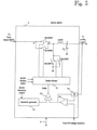
- FIG. 3 An example schematic diagram of a sectioned Buck switched-mode power supply (SMPS) according to an embodiment of the invention is shown in Figure 3 .
- the voltage V 2 i.e. the boosted voltage or the bypassed battery voltage V BATT
- V BATT bypassed battery voltage
- Parallel high-side switches BUHSW1 and BUHSW2 are coupled between the node D and a node E
- parallel low-side switches BULSW1 and BULSW2 are connected between the node E and a ground potential, for example.
- a buck inductor L buck is connected between the node E and the output node F.
- a buck capacitor C2 is connected between the node F and the ground potential.
- the control inputs of switches BUHSW1, BUHSW2, BULSW1 and BULSW2 are controlled by respective control signals from a switch driver 31.
- the switch driver 31 turns selected ones of the boost switches BUHSW1, BUHSW2, BULSW1 and BULSW2 ON (conductive) and OFF (non-conductive) under the control of a pulse width modulated (PWM) signal having a predetermined switching frequency.
- PWM pulse width modulated
- the switching frequency is generated by a switching frequency generator, such as a sawtooth waveform generator 32.
- the switching frequency may be set by a buck frequency control signal.
- the sawtooth waveform from the generator 32 may be applied to a first input of a comparator 33, such as a Smith trigger.
- the voltage V 1 at the output node F is coupled via a feedback network 34 to a first input of a further comparator 35.
- An envelope or voltage control signal from the PA voltage control circuit 6 may be applied to a second input of the comparator 35.
- An output voltage of the comparator 35 is thus proportional to the difference between the envelope information (representing the desired buck voltage) and the actual output voltage V 1 , and it is applied to a second input of the comparator 33.
- the state of the output from the comparator 33 changes each time the level of the sawtooth waveform exceeds the output voltage from the comparator 35.
- a PWM signal is provided whose frequency is set by the frequency of the sawtooth signal and whose duty cycle is set by the difference between the desired and actual buck voltage V 1 .
- the buck section select and the buck frequency control may be obtained through the control bus/line 9 from a transmitter control unit 8. It should be appreciated that this is only one example of many possible ways to implement the switch drive and control.
- the Buck SMPS 3 may be configured to have three section modes. In the first section mode, all switches BUHSW1, BUHSW2, BULSW1 and BULSW2 are selected. In the second section mode, the switches BUHSW1 and BULSW1 are selected. In the third section mode, the switches BUHSW2 and BULSW2 are selected.
- One example of possible sizing of switches BUHSW1, BUHSW2, BULSW1 and BULSW2 is similar to that described in connection with the Boost SMPS 2 in Figure 2 . However, it should be appreciated that the invention is not intended to be restricted to the sizing presented in that example but the sizing can be freely chosen for each application, depending on the number of parallel switches, the number of desired section modes, the type and number of different loads, for example.
- the Buck SMPS 3 shown in Figure 3 may be configured to have two section modes.
- the switches BUHSW1, BUHSW2, BULSW1 and BULSW2 may be selected, and in the second section mode, the switches BUHSW1 and BULSW1 or the switches BUHSW2 and BULSW2 may be selected.
- the switches BUHSW1 and BULSW1 are sized for a full load (e.g.
- BUHSW1 and BULSW1 may be selected in the first section mode and BUHSW2 and BULSW2 may be selected in the second section mode.
- two or three section modes provide a sufficient improvement in the performance in comparison with the complexity and cost of the additional control.
- the frequency control allows changing the switching frequency of the Boost SMPS 2 and the Buck SMPS 3 for different modes.
- Some modes, such as those using EER, ET or PT require relatively high switching frequency in order to achieve the required accuracy.
- a high switching frequency decreases the efficiency with increasing switching losses (parasitic capacitances of a switching stage and its control gates are charged and discharged at the switching frequency). Therefore, efficiency can be improved by lowering the switching frequency in the modes where it is possible.
- the frequency control may also include a dithering mode where the frequency is changed randomly from cycle to cycle. Dithering spreads the switching frequency spuriously over a wider band and thus reduces the average spur power density.
- the Boost SMPS 2 and the Buck SMPS 3 in cascade connection are controlled so that high efficiency is maintained for various loads and transmission power levels.
- the Boost SMPS 2 and the Buck SMPS 3 may be controlled based on the mode of operation of the transmitter, such as the actual battery voltage, the needed output power, the selected frequency band, the selected RF power amplifier (PA), the selected modulation method of the transmission signal, and/or the selected PA voltage control method, such as the envelope elimination and restoration (EER) technique, the envelope tracking (ET) technique, or the power-level tracking (PT).
- EER envelope elimination and restoration
- ET envelope tracking
- PT power-level tracking
- the Boost SMPS 2 may be switched off and put into a bypass mode when the battery voltage V BATT exceeds by a certain amount the actual needed collector voltage of a PA, so as to decrease the switching losses and to enhance efficiency.
- the supply currents taken by a PA may be different for the same collector voltage depending on the frequency band and mode of operation selected. For example, the highest supply currents are needed for the GSM900 transmission at the maximum power level, and thereby the first section mode enabling the high currents may be selected in the Boost SMPS 2 and/or Buck SMPS 3. For WCDMA, for example, the maximum currents and needed voltages are much less. Therefore, with the nominal battery voltage the Boost SMPS 2 may be bypassed for all WCDMA power levels and/or the second or third section mode may be selected in the Buck SMPS 3 in order to enhance efficiency.
- the switching frequency of Buck SMPS 3 can be reduced to decrease the switching losses, because there is no need for fast changes in voltage and the PA is also less sensitive to the ripple in collector voltage when used in the linear mode of operation, such as the PT.
- the GSM PA collector voltage is controlled according to the EER or the ET technique, higher accuracy and a higher switching frequency of the Buck SMPS 3 is required.
- Control of the transmitter may be provided from a transmitter control unit 8 that may be implemented by a control unit controlling the whole operation of a wireless communication device, such a cellular telephone.
- the control unit 8 may select a mode of operation for a multimode multiband wireless communication device and configure the RF power amplifiers 4 and 5 as well as the transmitter front stages 10 accordingly.
- the switches BHSW1, BHSW2, BLSW1 and BLSW2 of the Boost SMPS 2 as well as the switches BUHSW1, BUHSW2, BULSW1 and BULSW2 of the Buck SMPS 3 are typically enabled only during the transmission of radio bursts, and disabled otherwise. Consequently, the RF PAs 4 and 5 may be energized only during the radio bursts.
- the PA voltage control unit 6 may include a digital-to-analog converter (DAC) for converting digital voltage control values into an analog signal.
- DAC digital-to-analog converter
- the digital voltage control value that is written to the DAC may range from 0 to 2048, whereby the value 2048 may give an output voltage of 4.7 V from the Buck SMPS 3.
- the control of the Boost and Buck SMPSs according to a battery voltage V BATT , the selected transmission power level, the selected PA (the selected frequency band) and/or the selected mode may be as described in the following with reference to Figures 4 and 5 .
- the boost switching frequency is set to a frequency 1 (e.g. 8 MHz) by means of the boost frequency control signal applied to the generator 22, step 43.
- a frequency 1 e.g. 8 MHz
- different buck switching frequencies 1 and 1' may be set for EER and ET, respectively.
- a lower frequency 1' may be used in the ET mode because it is more linear than EER.
- fast envelope tracking is easier achieved with a higher switching frequency, such as that used for EER.
- the boost switching frequency is set to a frequency 2 (e.g. 5 MHz) in step 42.
- the battery voltage V BATT is measured during transmitting burst or shortly before the start of the transmitter TX, step 44.
- step 45 it is checked whether the measured V BATT is lower than the desired PA supply voltage V 1 (e.g. power scale*4.7V/2048) plus preset headroom (e.g. 0.6 V) needed by the Buck SMPS 3 (i.e. V 2 -V 1 ).
- V 1 e.g. power scale*4.7V/2048
- preset headroom e.g. 0.6 V
- the bypass switch BPSW1 is activated to connect the battery voltage directly to the output node C and the Buck SMPS 3, step 46.
- the value of the boost voltage V 2 is set to be slightly higher than the desired PA supply voltage V 1 plus the preset headroom (e.g. 0,6 V) by means of the boost voltage control signal applied to the comparator 25, step 47.
- step 48 it is checked whether the modulation method is GMSK (in the GSM mode) or WCDMA. If the modulation method is WCDMA, the Boost SMPS 2 is set to the second section mode (boost switches BHSW2 and BLSW2 are selected), step 49.
- step 50 If the modulation method is GSMK in step 48, it is then checked whether the high band PA 4 or the low band PA 5 is used, step 50. If the low band PA 5 is used, the Boost SMPS 2 is set to the first section mode (all boost switches are selected) by means of the boost section select signal, step 51. If the high band PA 4 is used, the Boost SMPS 2 is set to the second section mode (boost switches BHSW1 and BLSW1 are selected), step 52.
- the buck switching frequency is set to a frequency 1 (e.g. 11 MHz) by means of the buck frequency control signal applied to the generator 32, step 63.
- a frequency 1 e.g. 11 MHz
- different buck switching frequencies 1 and 1' may be set for EER and ET, respectively.
- a lower frequency 1' may be used in the ET mode because it is more linear than EER.
- fast envelope tracking is easier achieved with a higher switching frequency, such as that used for EER.
- the transmitter does not operate in the EER or ET mode, it is assumed that the PA is operating in a substantially linear mode (such the PT mode) and the buck switching frequency is set to a frequency 2 (e.g. 6 MHz) in step 62.
- step 64 it is checked whether the modulation method is GSMK or WCDMA. If the modulation method is GMSK, it checked whether the high band PA 4 or the low band PA 5 is used, step 65.
- the Buck SMPS 3 is set to the third section mode (the switches BUHSW2 and BULSW2 are selected), step 70.
- the Buck SMPS 3 is set to the third section mode (the switches BUHSW2 and BULSW2 are selected), step 70.
- step 64 If it is determined in step 64 that the modulation method is WCDMA, it is checked whether the high band PA 4 or the low band PA 5 is used, step 73.
- the Buck SMPS 3 is set to the third section mode (the switches BUHSW2 and BULSW2 are selected), step 76.
- threshold values for mode selection switching are presented above as illustrative examples only and they may change, depending on the switched-mode power supplies SMPS and the RF power amplifiers PA used in each particular transmitter, for example.
- RF power amplifiers of different manufacturers may typically have different currents and collector voltages.
- the used threshold values may be stored in a table format in the communication device.
- the threshold value tables may be created by measuring several power amplifiers from different manufacturers and comparing the voltage/current curves with the measured SMPS efficiency curves, or the tables may be individually tuned in production by searching the optimum switchover points (lowest battery current at that output voltage).
- Control functions may be implemented by various means.
- these functions, or the control unit 8 may be implemented in hardware (one or more devices), firmware (one or more devices), software (one or more modules), or combinations thereof.
- the processing units used for channel estimation may be implemented within one or more application specific integrated circuits (ASICs), digital signal processors (DSPs), digital signal processing devices (DSPDs), programmable logic devices (PLDs), field programmable gate arrays (FPGAs), processors, controllers, microcontrollers, microprocessors, other electronic units designed to perform the functions described herein, or a combination thereof.
- ASICs application specific integrated circuits
- DSPs digital signal processors
- DSPDs digital signal processing devices
- PLDs programmable logic devices
- FPGAs field programmable gate arrays
- processors controllers, microcontrollers, microprocessors, other electronic units designed to perform the functions described herein, or a combination thereof.
- firmware or software implementation can be through modules (e.g., procedures, functions)
- the software codes may be stored in a memory unit and executed by the processors.
- the memory unit may be implemented within the processor or external to the processor, in which case it can be communicatively coupled to the processor via various means as is known in the art. Additionally, components of the systems described herein may be rearranged and/or complemented by additional components in order to facilitate achieving the various aspects, goals, advantages, etc., described herein, and are not limited to the precise configurations set forth in a given figure, as will be appreciated by one skilled in the art.
- control unit 8 may be a transmitter control unit 8 or a control unit controlling the whole operation of a wireless communication device, such as a cellular telephone.
- Boost-type and Buck-type switched-mode power supplies, power amplifiers, and transmitters may be implemented with discrete electronic components, with one or more circuit chips, or with any combination of discrete components and one or more integrated chips.
- Integrated chips may use any suitable integrated circuit manufacturing technology, including bipolar, CMOS, and BiCMOS technologies.
Abstract
Description
- The present invention relates to switched-mode power supplies, and more specifically to switched-mode power supplies and their control methods for radio frequency (RF) power amplifiers in battery-powered wireless transmitter devices.
- Energy-efficient radio frequency (RF) power amplifiers (PA) are critical components in mobile, battery-operated wireless communication devices, e.g. mobile phones, personal digital assistants (PDA), etc., because they determine a significant portion of the total power consumption of such devices. Batteries with low supply voltage, typically about 3V, are employed in the portable devices. It has been possible to design a PA for the 3V battery voltage even if the efficiency already has dropped a bit. In order to get high efficiency from a PA, a switching-mode power supply (SMPS), often referred to as a Boost converter or a step-up converter is needed to up-convert the battery voltage to a value higher than the maximum battery voltage. With this approach, the needed output transmission power can be easily obtained from the PA, but the efficiency for small transmission power levels is poor. To improve efficiency also at the small transmission power levels, the supply voltage of the PA must be lowered. This is not possible with a Boost-type power supply but another type of switching-mode power supply (often referred to as a Buck converter, or a step-down converter) is provided to down-convert the raised battery voltage to the level needed for actual transmission power level. If the two converters are cascaded, the efficiency at low transmission power levels suffers from the cascaded converters and the high voltage between them.
- Some RF PA applications with a switching-mode power supply (SMPS) use a dynamic biasing PA, such as the envelope elimination and restoration (EER) technique, to achieve high-efficiency, linear power amplification. In the EER, the phase and envelope information are extracted from the original modulated signal. A constant envelope signal containing the phase information is amplified using an RF PA. Since the phase information has a constant envelope, the PA can be highly overdriven to achieve high efficiency. The envelope information is fed into the power supply circuit to modulate the supply voltage of the RF PA (e.g. drain or collector voltage) and thereby superimpose the envelope variation. By changing the supply voltage, the output waveform will be shaped and the overall amplification can be linear. There are also simplified versions of the EER, such as the envelope tracking (ET) technique. In the ET technique, the input signal to the RF amplifier contains both the phase information and the amplitude information, and only the envelope information is extracted for the switching power supply. The RF PA is operated in the linear region and its supply voltage is changed according to the extracted envelope information. The supply voltage is varied with sufficient headroom to minimize distortion. Examples of transmitter architectures employing EER technique are disclosed in
US 6,256,482 andWO2006/085,177 . A still further version is power-level tracking (PT) in which a switching-mode power supply tracks only the slow-varying average power level, instead of the fast-varying envelope, and modulates the drain or collector voltage of a linear PA. - So-called Buck-Boost converters also exist. An example of a Buck-Boost converter is disclosed in
US Patent 6,348,781 . The Buck-Boost converters are designed to change mode from Buck to Boost automatically to provide a supply voltage that ensures good efficiency of an RF PA at any specific transmission power level. No cascading is needed. However, in applications that use the envelope elimination and restoration (EER) technique, a very tightly controlled frequency and group delay response is needed. With a Buck-Boost switching-mode power supply, the output voltage range where the mode changes is quite critical, and distortion occurs. Also, in the Boost mode of operation it is difficult to keep the response unaffected. Buck-Boost converters are good choices for power level tracking where the frequency and group delay requirements are loose. - The problems regarding efficiency are becoming more significant with the battery technology, e.g. lithium battery technology, lowering the cut of voltage from the present range, e.g. 3V, to about 2.5V or lower. As a consequence, a transmission (TX) power amplifier becomes very inefficient and variation in its performance increases, if it is designed for 2.3V supply voltage, for example.
- Some aspects of the present invention are disclosed in the attached independent claims. Various embodiments of the invention are disclosed in the dependent claims.
- According to an aspect of the invention, a control method comprises
- measuring a battery voltage inputted to a cascade connection of a boost-type switched-mode power supply and a buck-type switched-mode power supply providing a supply voltage to a radio frequency power amplifier;
- comparing the measured battery voltage with a threshold corresponding to an input supply voltage which is needed for the buck-type switched-mode power supply;
- bypassing the boost-type switched-mode power supply and coupling the battery voltage directly to the buck-type switched-mode power supply, if the measured battery voltage exceeds the needed input supply voltage;
- controlling the boost-type switched-mode power supply to raise the battery voltage to at least the needed input supply voltage, if the measured battery voltage is below the needed input supply voltage;
- controlling the buck-type switched-mode power supply to operate in one of at least two section modes according to one or more of the following: a mode of operation of the power amplifier, a frequency band of the power amplifier, a modulation method, and a transmission power of the power amplifier.
- According to a further aspect of the invention, an apparatus comprises
- at least one radio frequency power amplifier;
- a boost-type switched-mode power supply having an input for a battery voltage from a battery;
- a buck-type switched-mode power supply connected in cascade with the boost-type switched-mode power supply and having a supply voltage output for the radio frequency power amplifier,
- a bypass switch controllable to bypass the boost-type switched-mode power supply and to couple the battery voltage directly to the buck-type switched-mode power supply, if the battery voltage exceeds a threshold corresponding to an input supply voltage which is needed for the buck-type switched-mode power supply;
- the boost-type switched-mode power supply being controllable to raise the battery voltage to at least the needed input supply voltage, if the battery voltage is below the threshold; and
- the buck-type switched-mode power supply comprising at least two section modes selectable according to one or more of the following: a mode of operation of the power amplifier, a frequency band of the power amplifier, a modulation method, and a transmission power of the power amplifier.
- According to a further aspect of the invention, a control method comprises
- providing a cascade connection of a boost-type switched-mode power supply and a buck-type switched-mode power supply to provide a supply voltage to a radio frequency power amplifier from a battery voltage;
- controlling the boost-type switched-mode power supply to raise the battery voltage to at least an input supply voltage which is needed for the buck-type switched-mode power supply;
- controlling the buck-type switched-mode power supply to operate in one of at least two section modes according to one or more of the following: a mode of operation of the power amplifier, a frequency band of the power amplifier, a modulation method, and a transmission power of the power amplifier.
- According to a further aspect of the invention, a control method comprises
- providing a cascade connection of a boost-type switched-mode power supply and a buck-type switched-mode power supply to provide a supply voltage to a radio frequency power amplifier from a battery voltage;
- controlling the boost-type switched-mode power supply to raise the battery voltage to at least an input supply voltage which is needed for the buck-type switched-mode power supply;
- controlling the buck-type switched-mode power supply to operate at a higher switching frequency, when the power amplifier operates in an envelope elimination and restoration (EER) mode or in an envelope tracking (ET) mode, and to operate at a lower switching frequency, when the power amplifier operates in a linear mode.
- Still another aspect of the invention is a computer program embodied on a computer readable medium, said computer program comprising a program code for controlling a processor to execute control methods according to various embodiments of the invention.
- Still another aspect of the invention is a controller comprising means for embodying control methods according to various embodiments of the invention.
- In the following the invention will be described in greater detail by means of exemplary embodiments with reference to the attached drawings, in which
-
Figure 1 is a block diagram illustrating an example of a transmitter according to an embodiment of the present invention; -
Figure 2 is a schematic diagram illustrating an example of a boost-type switched-mode power supply according an embodiment of the invention; -
Figure 3 is a schematic diagram illustrating an example of a buck-type switched-mode power supply according an embodiment of the invention; -
Figure 4 is a flow diagram illustrating an example of a control algorithm for controlling a boost-type switched-mode power supply in accordance with an embodiment of the invention; and -
Figure 5 is a flow diagram illustrating an example of a control algorithm for controlling a buck-type switched-mode power supply in accordance with an embodiment of the invention. - Referring to
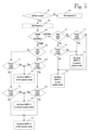
Figure 1 , a block diagram of an exemplary RF transmitter (TX) circuitry is shown in which a supply voltage is provided from abattery 1 to power amplifiers (PA) 4, 5 through cascaded Boost and Buck switched-mode power supplies (SMPS) 2, 3. - A
battery 1 provides a battery voltage Vbatt to a Boost-type switchedmode power supply 2 according to an embodiment of the invention. The battery may be any type of battery suitable for portable devices, such as a lithium cell battery or a nickel cadmium battery. The battery voltage Vbatt may have any low voltage value depending on the application and the battery technology selected. A typical battery voltage may be about 3 Volts or lower, or even 2.5 Volts or lower. - The Boost switched-
mode power supply 2 up-converts from the battery voltage Vbatt a supply voltage V2 with a raised voltage level to a Buck-type switched-mode power supply 3. The Boost switched-mode power supply may also include a bypass function that bypasses the battery voltage Vbatt to form the supply voltage V2 to the Buck-type switched-mode power supply 3 without boosting. The Boost switched-mode power supply 2 may also include sectioned transistor switches as will be described below. A boost condensator C1 filters high-frequency interference from the boosted voltage V2. - The Buck-type switched-
mode power supply 3 down-converts from the supply voltage V2 a supply voltage V1 for the RF power amplifiers (PA) 4 and 5. The Buck-type switched-mode power supply 3 may also include sectioned transistor switches as will be described below. TheBuck SMPS 3 may provide a biasing control for thePAs PAs voltage control unit 6 in the transmitter circuitry may provide a PA voltage control signal to theBuck SMPS 3. For example, for the envelope elimination and restoration (EER) technique, envelope tracking (ET) technique, or power-level tracking (PT), the PA voltage control signal from thecontrol unit 6 may represent envelope information derived from the modulated signal, so that the voltage control signal causes theBuck SMPS 3 to modulate the supply voltage V1. In an embodiment, theBuck SMPS 3 may be controlled directly with duty cycle information (command) when theBuck SMPS 3 has an internal duty cycle generator. In another embodiment, a control signal required with the wanted duty cycle is sent to the input of a switch driver in theBuck SMPS 3. - Nowadays, mobile communication devices are often multimode and multiband devices supporting two or more frequency bands and modulation formats (for example, GSM, EDGE, CDMA, WCDMA). It is logical to use as few RF power amplifiers as possible but typically at least a low frequency band (such as 900 MHz band for GSM/EDGE/WCDMA) and a high frequency band (such as 1800/1900 MHz band for GSM/EDGE/WCDMA) use different RF power amplifiers even if the amplifiers were implemented inside the same RF module and even on the same chip. In the embodiment shown in
Figure 1 , there are two RF power amplifiers (PAs), theRF PA 4 for a high frequency band (e.g. 1800/1900 MHz) of one or more systems (such as GSM, CDMA, WCDMA), and theRF PA 5 for a low frequency band (such as 900 MHz) of one or more systems (such as GSM, CDMA, WCDMA). However, the present invention is not intended to be restricted to this number of power amplifiers but all bands may be implemented by means of one power amplifier, or there may be more power amplifiers with dedicated frequency bands. It should also be appreciated that the mobile communication systems and frequency bands mentioned are only examples, and the present invention can be applied to any mobile communication systems and frequency bands. - A power amplifier may have several different modes of operation, for example a linear mode for the envelope tracking (ET) and power tracking (PT) operation, and a compressed mode for the EER operation. The needed transmission output powers are different for different cellular systems and frequency bands. For instance, for the GSM900 system the needed maximum output power may be 2W or 33dBm, for the GSM1800 system the needed maximum output power may be 1W (30dBm), and for WCDMA on both bands the needed maximum output power may 24 dBm on average. If the output matching of RF PAs is fixed (could also be switchable), the RF PAs are usually designed so that the maximum wanted power is obtained with a certain collector voltage, for example 4.5V. When lower power is needed, the collector voltage can be reduced and this may be achieved with a buck converter. Also, the needed amount of current with maximum output power is less for the high frequency band (1W versus 2W in the example above). Because the same switched-mode power supplies feed the PAs operating in different frequency bands and thereby with different transmission powers, the SMPSs need to be designed for the heaviest load (in the example above, to feed the GSM900 band requires a maximum power of 2W). When another PA or another modulation or a lower output power is used, the efficiency of the SMPSs is not optimum.
- According to embodiments of the invention, the Buck-type SMPS or the Boost-type SMPS or both may be configured to be sectioned SMPSs. In other words, the transistor switches may be implemented with parallel transistors, instead of single transistors, so that it is possible to selectively use some or all of the parallel transistors according to the load at each specific moment and thus reduce the capacitive switching losses.
- An example schematic diagram of a sectioned bypass Boost switched-mode power supply (SMPS) according to an embodiment of the invention is shown in
Figure 2 . The battery voltage VBATT from thebattery 1 at an input node A is coupled to one end of a boost inductor Lboost, the second end of which is coupled to a circuit node B. Avoltage meter 26 may be provided to measure the battery voltage and to forward the measurement result to a control unit 8 via a control bus/line 9. Parallel high-side switches BHSW1 and BHSW2 are coupled between the node B and an output node C, and parallel low-side switches BLSW1 and BLSW2 are connected between the node B and a ground potential, for example. A bypass switch BPSW1 may further be connected between the input node A and the output node C to selectively bypass the boost inductor Lboost and the high-side switches BHSW1 and BHSW2, and thereby to couple the battery voltage VBATT directly to theBuck SMPS 3. The control inputs of switches BHSW1, BHSW2, BLSW1, BLSW2 and BPSW1 are controlled by respective control signals from aswitch driver 21. Depending on the Boost section mode selected according to a boost section select control input, theswitch driver 21 turns selected boost switches BHSW1, BHSW2, BLSW1 and BLSW2 ON (conductive) and OFF (non-conductive) under the control of a pulse width modulated (PWM) signal having a predetermined switching frequency. The switching frequency is generated by a switching frequency generator, such as asawtooth waveform generator 22 inFigure 2 . The switching frequency may be set by a boost frequency control signal. The sawtooth waveform from thegenerator 22 may be applied to a first input of acomparator 23, such as a Smith 'trigger. The voltage V2 at the output node C is coupled via afeedback network 24 to a first input of afurther comparator 25. A boost voltage control signal that determines the desired boost voltage V2 is applied to a second input of thecomparator 25. An output voltage of thecomparator 25 is thus proportional to the difference between the desired boost voltage and the actual output voltage V2, and it is applied to a second input of acomparator 23. The state of the output from thecomparator 23 changes each time the level of the sawtooth waveform exceeds the output voltage from thecomparator 25. Thereby a PWM signal is provided whose frequency is set by the frequency of the sawtooth signal and whose duty cycle is set by the difference between the desired and actual boost voltage V2. If the bypass switch BPSW1 is turned on, and the Boost SPMS is bypassed, all boost switches BHSW1, BHSW2, BLSW1 and BLSW2 may be turned off, or the high side switches BHSW1 and BHSW2 may be kept on in order to decrease the total resistance from battery to output because the current flows through the high side switches and the bypass switch. The latter arrangement allows to size the bypass switch smaller and thereby saves chip area in integrated implementations. The boost section select, the boost frequency control, and the boost voltage control may be obtained through the control bus/line 9 from a transmitter control unit 8. It should be appreciated that this is only one example of many possible ways to implement the switch drive and control. - In an embodiment of the invention, the
Boost SMPS 2 may be configured to have three section modes. In the first section mode, all switches BHSW1, BHSW2, BLSW1 and BLSW2 are selected. In the second section mode, the switches BHSW1 and BLSW1 are selected. In the third section mode, the switches BHSW2 and BLSW2 are selected. One example of possible sizing of switches BHSW1, BHSW2, BLSW1 and BLSW2, when field effect transistors (FETs) are used, could be as follows. If the needed FET size for maximum current is W=21 mm (wherein W is a channel width whose value depends on a needed switch resistance), this maximum size could be split between two parallel FETs, so that a first FET (e.g. BHSW1 and BLSW1) has a size W=14mm and a second FET (e.g. BHSW2 and BLSW2) has a size W=7mm. Thus, in the first section mode, when both parallel switches BHSW1 and BHSW2, or BLSW1 and BLSW2, respectively, are activated, the total effective width of the parallel switches is 21mm. In the second section mode, when only the bigger switch, BHSW1 and BLSW1, is selected in each pair of parallel switches, the active size is 14mm. Similarly, in the third section mode, when only the smaller switch, BHSW2 and BLSW2, is selected in each pair of parallel switches, the active size is 7mm. As a result, the driving losses are reduced to two 3rds in the second section mode and to one 3rd in the third section mode in relation to the first section mode, i.e. the full load. It should be appreciated that the invention is not intended to be restricted to the sizing presented in the above example but the sizing can be freely chosen for each application, depending on the number of parallel switches, the number of desired section modes, the type and number of different loads, for example. - It should also be appreciated that the number of different section modes can be freely chosen for each application. In an embodiment of the invention, there is no sectioning of the boost switches at all, and bypass switching is implemented. In an embodiment of the invention, the
Boost SMPS 2 shown inFigure 2 may be configured to have two section modes. With the exemplary sizing described above, in the first section mode, all switches BHSW1, BHSW2, BLSW1 and BLSW2 may be selected, and in the second section mode, the switches BHSW1 and BLSW1 or the switches BHSW2 and BLSW2 may be selected. As another example, if the switches BHSW1 and BLSW1 are sized for a full load (e.g. W=21mm) and the switches BHSW2 and BLSW2 are sized for a half load (e.g. W=10mm), BHSW1 and BLSW1 may be selected in the first section mode and BHSW2 and BLSW2 may be selected in the second section mode. In most applications, two or three section modes provide a sufficient improvement in the performance in comparison with the complexity and cost of the additional control. - An example schematic diagram of a sectioned Buck switched-mode power supply (SMPS) according to an embodiment of the invention is shown in
Figure 3 . The voltage V2 (i.e. the boosted voltage or the bypassed battery voltage VBATT) from theBoost SMPS 2 is inputted to theBuck SMPS 3 at an input node D. Parallel high-side switches BUHSW1 and BUHSW2 are coupled between the node D and a node E, and parallel low-side switches BULSW1 and BULSW2 are connected between the node E and a ground potential, for example. A buck inductor Lbuck is connected between the node E and the output node F. A buck capacitor C2 is connected between the node F and the ground potential. The control inputs of switches BUHSW1, BUHSW2, BULSW1 and BULSW2 are controlled by respective control signals from aswitch driver 31. Depending on the Buck section mode selected according to a buck section select control input, theswitch driver 31 turns selected ones of the boost switches BUHSW1, BUHSW2, BULSW1 and BULSW2 ON (conductive) and OFF (non-conductive) under the control of a pulse width modulated (PWM) signal having a predetermined switching frequency. The switching frequency is generated by a switching frequency generator, such as asawtooth waveform generator 32. The switching frequency may be set by a buck frequency control signal. The sawtooth waveform from thegenerator 32 may be applied to a first input of acomparator 33, such as a Smith trigger. The voltage V1 at the output node F is coupled via afeedback network 34 to a first input of afurther comparator 35. An envelope or voltage control signal from the PAvoltage control circuit 6 may be applied to a second input of thecomparator 35. An output voltage of thecomparator 35 is thus proportional to the difference between the envelope information (representing the desired buck voltage) and the actual output voltage V1, and it is applied to a second input of thecomparator 33. The state of the output from thecomparator 33 changes each time the level of the sawtooth waveform exceeds the output voltage from thecomparator 35. Thereby a PWM signal is provided whose frequency is set by the frequency of the sawtooth signal and whose duty cycle is set by the difference between the desired and actual buck voltage V1. The buck section select and the buck frequency control may be obtained through the control bus/line 9 from a transmitter control unit 8. It should be appreciated that this is only one example of many possible ways to implement the switch drive and control. - In an embodiment of the invention, the
Buck SMPS 3 may be configured to have three section modes. In the first section mode, all switches BUHSW1, BUHSW2, BULSW1 and BULSW2 are selected. In the second section mode, the switches BUHSW1 and BULSW1 are selected. In the third section mode, the switches BUHSW2 and BULSW2 are selected. One example of possible sizing of switches BUHSW1, BUHSW2, BULSW1 and BULSW2 is similar to that described in connection with theBoost SMPS 2 inFigure 2 . However, it should be appreciated that the invention is not intended to be restricted to the sizing presented in that example but the sizing can be freely chosen for each application, depending on the number of parallel switches, the number of desired section modes, the type and number of different loads, for example. - It should also be appreciated that the number of different section modes can be freely chosen for each application, in a manner similar to that described in connection with the
Boost SMPS 2 inFigure 2 . Thus, in an embodiment of the invention, theBuck SMPS 3 shown inFigure 3 may be configured to have two section modes. With the exemplary sizing described above, in the first section mode, all switches BUHSW1, BUHSW2, BULSW1 and BULSW2 may be selected, and in the second section mode, the switches BUHSW1 and BULSW1 or the switches BUHSW2 and BULSW2 may be selected. As another example, if the switches BUHSW1 and BULSW1 are sized for a full load (e.g. W=21mm) and the switches BUHSW2 and BULSW2 are sized for a half load (e.g. W=10mm), BUHSW1 and BULSW1 may be selected in the first section mode and BUHSW2 and BULSW2 may be selected in the second section mode. In most applications, two or three section modes provide a sufficient improvement in the performance in comparison with the complexity and cost of the additional control. - The frequency control allows changing the switching frequency of the
Boost SMPS 2 and theBuck SMPS 3 for different modes. Some modes, such as those using EER, ET or PT require relatively high switching frequency in order to achieve the required accuracy. A high switching frequency decreases the efficiency with increasing switching losses (parasitic capacitances of a switching stage and its control gates are charged and discharged at the switching frequency). Therefore, efficiency can be improved by lowering the switching frequency in the modes where it is possible. In an embodiment of the invention, the frequency control may also include a dithering mode where the frequency is changed randomly from cycle to cycle. Dithering spreads the switching frequency spuriously over a wider band and thus reduces the average spur power density. - According to embodiments of the invention, the
Boost SMPS 2 and theBuck SMPS 3 in cascade connection are controlled so that high efficiency is maintained for various loads and transmission power levels. TheBoost SMPS 2 and theBuck SMPS 3 may be controlled based on the mode of operation of the transmitter, such as the actual battery voltage, the needed output power, the selected frequency band, the selected RF power amplifier (PA), the selected modulation method of the transmission signal, and/or the selected PA voltage control method, such as the envelope elimination and restoration (EER) technique, the envelope tracking (ET) technique, or the power-level tracking (PT). - For example, in an embodiment of the invention, because the switching losses depend directly on the voltage range over which the signal is swinging, the
Boost SMPS 2 may be switched off and put into a bypass mode when the battery voltage VBATT exceeds by a certain amount the actual needed collector voltage of a PA, so as to decrease the switching losses and to enhance efficiency. - The supply currents taken by a PA may be different for the same collector voltage depending on the frequency band and mode of operation selected. For example, the highest supply currents are needed for the GSM900 transmission at the maximum power level, and thereby the first section mode enabling the high currents may be selected in the
Boost SMPS 2 and/orBuck SMPS 3. For WCDMA, for example, the maximum currents and needed voltages are much less. Therefore, with the nominal battery voltage theBoost SMPS 2 may be bypassed for all WCDMA power levels and/or the second or third section mode may be selected in theBuck SMPS 3 in order to enhance efficiency. - As a further example, according to an embodiment of the invention, if the WCDMA PA collector voltage is controlled according to the power level (the PT technique), then the switching frequency of
Buck SMPS 3 can be reduced to decrease the switching losses, because there is no need for fast changes in voltage and the PA is also less sensitive to the ripple in collector voltage when used in the linear mode of operation, such as the PT. On the other hand, if the GSM PA collector voltage is controlled according to the EER or the ET technique, higher accuracy and a higher switching frequency of theBuck SMPS 3 is required. - In the following, examples of the operation of the transmitter and the control of the Boost and Buck SMPSs according to embodiments of the invention are described.
- Control of the transmitter may be provided from a transmitter control unit 8 that may be implemented by a control unit controlling the whole operation of a wireless communication device, such a cellular telephone. The control unit 8 may select a mode of operation for a multimode multiband wireless communication device and configure the
RF power amplifiers - The switches BHSW1, BHSW2, BLSW1 and BLSW2 of the
Boost SMPS 2 as well as the switches BUHSW1, BUHSW2, BULSW1 and BULSW2 of theBuck SMPS 3 are typically enabled only during the transmission of radio bursts, and disabled otherwise. Consequently, theRF PAs - When a transmitter (TX) is needed to start, the first step is to start the
Boost SMPS 2. Then theBuck SMPS 3 is started and needed control voltage from PAvoltage control unit 6 is set. The PAvoltage control unit 6 may include a digital-to-analog converter (DAC) for converting digital voltage control values into an analog signal. For example, the digital voltage control value that is written to the DAC may range from 0 to 2048, whereby the value 2048 may give an output voltage of 4.7 V from theBuck SMPS 3. Alternatively, it is also possible to control thebuck SMPS 3 directly with duty cycle information (command), if thebuck SMPS 3 has an internal duty cycle generator, or send an input signal required with the wanted duty cycle (e.g. a signal similar to the PWM signal inFigure 3 ) to the input ofswitch driver 31. - The control of the Boost and Buck SMPSs according to a battery voltage VBATT, the selected transmission power level, the selected PA (the selected frequency band) and/or the selected mode may be as described in the following with reference to
Figures 4 and5 . - Referring to
Figure 4 , it is first checked whether the transmitter operates in the EER or ET mode instep 41. If the transmitter operates in the EER or ET mode, the boost switching frequency is set to a frequency 1 (e.g. 8 MHz) by means of the boost frequency control signal applied to thegenerator 22,step 43. In an embodiment of the invention, differentbuck switching frequencies 1 and 1' may be set for EER and ET, respectively. A lower frequency 1' may be used in the ET mode because it is more linear than EER. However, fast envelope tracking is easier achieved with a higher switching frequency, such as that used for EER. If the transmitter does not operate in the EER or ET mode, the boost switching frequency is set to a frequency 2 (e.g. 5 MHz) instep 42. - The battery voltage VBATT is measured during transmitting burst or shortly before the start of the transmitter TX,
step 44. Instep 45, it is checked whether the measured VBATT is lower than the desired PA supply voltage V1 (e.g. power scale*4.7V/2048) plus preset headroom (e.g. 0.6 V) needed by the Buck SMPS 3 (i.e. V2-V1). - If the measured VBATT is higher than the desired PA supply voltage V1 plus the preset headroom (e.g. 0.6 V), the bypass switch BPSW1 is activated to connect the battery voltage directly to the output node C and the
Buck SMPS 3,step 46. - If the measured VBATT is lower than the desired PA supply voltage V1 plus the preset headroom (e.g. 0,6 V), the value of the boost voltage V2 is set to be slightly higher than the desired PA supply voltage V1 plus the preset headroom (e.g. 0,6 V) by means of the boost voltage control signal applied to the
comparator 25,step 47. - In
step 48, it is checked whether the modulation method is GMSK (in the GSM mode) or WCDMA. If the modulation method is WCDMA, theBoost SMPS 2 is set to the second section mode (boost switches BHSW2 and BLSW2 are selected),step 49. - If the modulation method is GSMK in
step 48, it is then checked whether thehigh band PA 4 or thelow band PA 5 is used,step 50. If thelow band PA 5 is used, theBoost SMPS 2 is set to the first section mode (all boost switches are selected) by means of the boost section select signal,step 51. If thehigh band PA 4 is used, theBoost SMPS 2 is set to the second section mode (boost switches BHSW1 and BLSW1 are selected),step 52. - Referring to
Figure 5 , it is first checked whether the transmitter operates in the EER or ET mode instep 61. If the transmitter operates in the EER or ET mode, the buck switching frequency is set to a frequency 1 (e.g. 11 MHz) by means of the buck frequency control signal applied to thegenerator 32,step 63. In an embodiment of the invention, differentbuck switching frequencies 1 and 1' may be set for EER and ET, respectively. A lower frequency 1' may be used in the ET mode because it is more linear than EER. However, fast envelope tracking is easier achieved with a higher switching frequency, such as that used for EER. If the transmitter does not operate in the EER or ET mode, it is assumed that the PA is operating in a substantially linear mode (such the PT mode) and the buck switching frequency is set to a frequency 2 (e.g. 6 MHz) instep 62. - In
step 64, it is checked whether the modulation method is GSMK or WCDMA. If the modulation method is GMSK, it checked whether thehigh band PA 4 or thelow band PA 5 is used,step 65. - If the
high band PA 4 is used, it is checked whether the selected power scale is equal to or higher than 1300,step 66. This corresponds to the PA supply voltage V1 having a value of approximately (1300*4.7V/2048=) 3V. If the power scale is equal to or higher than 1300, theBuck SMPS 3 is set to the first section mode (all buck switches are selected) by means of the buck section select signal,step 67. - If the power scale is lower than 1300, it is checked whether the selected power scale is equal to or higher than 650,
step 68. This corresponds to the PA supply voltage V1 having a value of approximately (650*4.7V/2048=) 1.5V. If the power scale is equal to or higher than 650, theBuck SMPS 3 is set to the second section mode (the switches BUHSW1 and BULSW1 are selected),step 69. - If the power scale is lower than 650, the
Buck SMPS 3 is set to the third section mode (the switches BUHSW2 and BULSW2 are selected),step 70. - If it is determined in step 55 that the
low band PA 5 is used, it is checked whether the selected power scale is equal to or higher than 800,step 71. This corresponds to the PA supply voltage V1 having a value of approximately (800*4.7V/2048=) 1.8V. If the power scale is equal to or higher than 800, theBuck SMPS 3 is set to the first section mode (all buck switches are selected) by means of the buck section select signal,step 67. - If the power scale is lower than 800, it checked whether the selected power scale is equal to or higher than 400,
step 72. This corresponds to the PA supply voltage V1 having a value of approximately (400*4.7V/2048=) 0.9V. If the power scale is equal to or higher than 400, theBuck SMPS 3 is set to the second section mode (the switches BUHSW1 and BULSW1 are selected),step 69. - If the power scale is lower than 400, the
Buck SMPS 3 is set to the third section mode (the switches BUHSW2 and BULSW2 are selected),step 70. - If it is determined in
step 64 that the modulation method is WCDMA, it is checked whether thehigh band PA 4 or thelow band PA 5 is used,step 73. - If the
high band PA 4 is used, it is checked whether the selected power scale is equal to or higher than 1400,step 74. This corresponds to the PA supply voltage V1 having a value of approximately (1400*4.7V/2048=) 3.2V. If the power scale is equal to or higher than 1400, theBuck SMPS 3 is set to the second section mode (the switches BUHSW1 and BULSW1 are selected) by means of the buck section select signal,step 75. - If it is determined in
step 63 that thelow band PA 5 is used, it is checked whether the selected power scale is equal to or higher than 900,step 77. This corresponds to the PA supply voltage V1 having a value of approximately (900*4.7V/2048=) 2.0V. If the power scale is equal to or higher than 900, theBuck SMPS 3 is set to the second section mode (the switches BUHSW1 and BULSW1 are selected) by means of the buck section select signal,step 75. - If the power scale is lower than 900, the
Buck SMPS 3 is set to the third section mode (the switches BUHSW2 and BULSW2 are selected),step 76. - It should be appreciate that the threshold values for mode selection switching are presented above as illustrative examples only and they may change, depending on the switched-mode power supplies SMPS and the RF power amplifiers PA used in each particular transmitter, for example. RF power amplifiers of different manufacturers may typically have different currents and collector voltages. The used threshold values may be stored in a table format in the communication device. The threshold value tables may be created by measuring several power amplifiers from different manufacturers and comparing the voltage/current curves with the measured SMPS efficiency curves, or the tables may be individually tuned in production by searching the optimum switchover points (lowest battery current at that output voltage).
- It should also be appreciated that the exemplary control algorithms described with respect to
Figures 4 and5 are intended only to illustrate the present invention, and that various different control algorithms can be applied without departing from the scope of the present invention. - Control functions according to various embodiments of the present invention may be implemented by various means. For example, these functions, or the control unit 8, may be implemented in hardware (one or more devices), firmware (one or more devices), software (one or more modules), or combinations thereof. For a hardware implementation, the processing units used for channel estimation may be implemented within one or more application specific integrated circuits (ASICs), digital signal processors (DSPs), digital signal processing devices (DSPDs), programmable logic devices (PLDs), field programmable gate arrays (FPGAs), processors, controllers, microcontrollers, microprocessors, other electronic units designed to perform the functions described herein, or a combination thereof. For firmware or software, implementation can be through modules (e.g., procedures, functions) that perform the functions described herein. The software codes may be stored in a memory unit and executed by the processors. The memory unit may be implemented within the processor or external to the processor, in which case it can be communicatively coupled to the processor via various means as is known in the art. Additionally, components of the systems described herein may be rearranged and/or complemented by additional components in order to facilitate achieving the various aspects, goals, advantages, etc., described herein, and are not limited to the precise configurations set forth in a given figure, as will be appreciated by one skilled in the art.
- According to some embodiments of the invention, the control unit 8 may be a transmitter control unit 8 or a control unit controlling the whole operation of a wireless communication device, such as a cellular telephone.
- Boost-type and Buck-type switched-mode power supplies, power amplifiers, and transmitters according to embodiments of the invention may be implemented with discrete electronic components, with one or more circuit chips, or with any combination of discrete components and one or more integrated chips. Integrated chips may use any suitable integrated circuit manufacturing technology, including bipolar, CMOS, and BiCMOS technologies.
- Furthermore, the following exemplary embodiments of the invention are to be understood to be disclosed:
- Embodiment 1: A control method, comprising
- measuring a battery voltage inputted to a cascade connection of a boost-type switched-mode power supply and a buck-type switched-mode power supply providing a supply voltage to a radio frequency power amplifier;
- comparing the measured battery voltage to a threshold corresponding an input supply voltage which is needed for the buck-type switched-mode power supply;
- bypassing the boost-type switched-mode power supply and coupling the battery voltage directly to the buck-type switched-mode power supply, if the measured battery voltage exceeds the needed input supply voltage;
- controlling the boost-type switched-mode power supply to raise the battery voltage to at least the needed input supply voltage, if the measured battery voltage is below the needed input supply voltage;
- controlling the buck-type switched-mode power supply to operate in one of at least two section modes according to one or more of: a mode of operation of the power amplifier, a frequency band of the power amplifier, a modulation method, and a transmission power of the power amplifier.
- Embodiment 2: A method according to
Embodiment 1, further comprising
controlling the buck-type switched-mode power supply to operate at one of at least two switching frequency according to one or more of: a mode of operation of the power amplifier, a frequency band of the power amplifier, a modulation method, and a transmission power of the power amplifier. - Embodiment 3: A method according to any one of
Embodiments
controlling the boost-type switched-mode power supply to operate at one of at least two switching frequency according to one or more of: a mode of operation of the power amplifier, a frequency band of the power amplifier, a modulation method, and a transmission power of the power amplifier. - Embodiment 4: A method according to any one of
Embodiments
controlling the boost-type switched-mode power supply to operate in one of at least two section modes according to one or more of: a mode of operation of the power amplifier, a frequency band of the power amplifier, a modulation method, and a transmission power of the power amplifier. - Embodiment 5: A method according to any one of
Embodiments
controlling the buck-type switched-mode power supply or the boost-type switched-mode power supply to operate at a higher switching frequency, when the power amplifier operates in an envelope elimination and restoration mode or in an envelope tracking mode, and to operate at a lower switching frequency, when the power amplifier operates in a power-level tracking mode. - Embodiment 6: A computer program embodied on a computer readable medium, the computer program comprising program code for controlling a processor to execute a method according to any one of Embodiments 1-5.
- Embodiment 7: An apparatus, comprising
- at least one radio frequency power amplifier;
- a boost-type switched-mode power supply having an input for a battery voltage from a battery ;
- a buck-type switched-mode power supply connected in cascade with the boost-type switched-mode power supply and having a supply voltage output for the radio frequency power amplifier,
- a bypass switch controllable to bypass the boost-type switched-mode power supply and to couple the battery voltage directly to the buck-type switched-mode power supply, if the battery voltage exceeds a threshold corresponding an input supply voltage which is needed for the buck-type switched-mode power supply;
- the boost-type switched-mode power supply is controllable to raise the battery voltage to at least the needed input supply voltage, if the battery voltage is below the threshold; and
- the buck-type switched-mode power supply comprises at least two section modes selectable according to one or more of: a mode of operation of the power amplifier, a frequency band of the power amplifier, a modulation method, and a transmission power of the power amplifier.
- Embodiment 8: An apparatus according to
Embodiment 7, wherein at least one of the buck-type switched-mode power supply and the boost-type switched-mode power supply is controllable to operate at one of at least two switching frequencies according to one or more of: a mode of operation of the power amplifier, a frequency band of the power amplifier, a modulation method, and a transmission power of the power amplifier. - Embodiment 9: An apparatus according to any one of
Embodiments 7 or 8, wherein the boost-type switched-mode power supply is controllable to operate in one of at least two section modes according to one or more of: a mode of operation of the power amplifier, a frequency band of the power amplifier, a modulation method, and a transmission power of the power amplifier. - Embodiment 10: An apparatus according to any one of
Embodiments 7 to 9, wherein the buck-type switched-mode power supply or the boost-type switched-mode power supply is controllable to operate at a higher switching frequency, when the power amplifier operates in an envelope elimination and restoration mode or in an envelope tracking mode, and to operate at a lower switching frequency, when the power amplifier operates in a power-level tracking mode. - Embodiment 11: An apparatus according to
Embodiment 10, wherein the switching frequencies are different for the boost-type switched-mode power supply and the buck-type switched-mode power supply. - Embodiment 12: An apparatus according to any one of
Embodiments 7 to 11, wherein the boost-type switched-mode power supply, the buck-type switched-mode power supply and the power amplifier are implemented with discrete electronic components, with one or more circuit chips, or with any combination of discrete electronic components and one or more integrated chips. - Embodiment 13: An apparatus according to any one of
Embodiments 7 to 12, wherein the apparatus is implemented in a radio frequency transmitter or in a wireless communication device. - Embodiment 14: A controller comprising means for embodying a control method according to any one of
Embodiments 1 to 6. - Embodiment 15: A controller according to Embodiment 14, wherein said means are implemented in hardware, firmware, software, or combinations thereon.
- The previous description of the disclosed embodiments is provided to enable any person skilled in the art to make or use the present invention. Various modifications to these embodiments will be readily apparent to those skilled in the art, and the generic principles defined herein may be applied to other embodiments without departing from the spirit or scope of the invention. Thus, the present invention is not intended to be limited to the embodiments described herein but is to be accorded the widest scope consistent with the principles and novel features disclosed herein.
Claims (15)
- A method, comprising:providing, by a buck-type switched-mode power supply, a supply voltage to a radio frequency power amplifier (4,5),configuring the buck-type switched-mode power supply to operate in one of at least two section modes.
- A method as claimed in claim 1, wherein the buck-type switched-mode power supply (3) section mode is selectable according to one or more of: a mode of operation of the power amplifier, a frequency band of the radio frequency power amplifier, a transmission power of the radio frequency power amplifier and a modulation method.
- A method as claimed in claim 1 or 2, further comprising:measuring (44) a battery voltage inputted to a cascade connection of a boost-type switched-mode power supply and a buck-type switched-mode power supply providing a supply voltage to a radio frequency power amplifier;comparing (45) the measured battery voltage to a threshold corresponding an input supply voltage which is needed for the buck-type switched-mode power supply;bypassing (46) the boost-type switched-mode power supply and coupling the battery voltage directly to the buck-type switched-mode power supply, if the measured battery voltage exceeds the needed input supply voltage;configuring (47) the boost-type switched-mode power supply to raise the battery voltage to at least the needed input supply voltage, if the measured battery voltage is below the needed input supply voltage.
- A method as claimed in claims 1 to 3, further comprising:
configuring (62,63) the buck-type switched-mode power supply to operate at one of at least two switching frequency according to one or more of: a mode of operation of the power amplifier, a frequency band of the power amplifier, a transmission power of the power amplifier and a modulation method. - A method as claimed in claims 1 to 4, further comprising:
configuring (42,43) the boost-type switched-mode power supply to operate at one of at least two switching frequency according to one or more of: a mode of operation of the power amplifier, a frequency band of the power amplifier, a transmission power of the power amplifier and a modulation method. - An apparatus, comprising:at least one radio frequency power amplifier (4,5);a buck-type switched-mode power supply (3) configured to provide a supply voltage to the radio frequency power amplifier (4,5),wherein the buck-type switched-mode power supply (3) comprises at least two section modes.
- An apparatus as claimed in claim 6, wherein the buck-type switched-mode power supply (3) section mode is selectable according to one or more of: a mode of operation of the radio frequency power amplifier, a frequency band of the radio frequency power amplifier, a transmission power of the radio frequency power amplifier and a modulation method.
- An apparatus as claimed in claims 6 or 7 further comprising:a boost-type switched-mode power supply (2) comprising an input for a battery voltage from a battery (1);wherein the buck-type switched-mode power supply (3) is coupled in cascade with the boost-type switched-mode power supply (2).
- An apparatus as claimed in claim 8 further comprising:
a bypass switch (BPSW1) configured to bypass the boost-type switched-mode power supply (2) and to couple the battery voltage directly to the buck-type switched-mode power supply (3), if the battery voltage exceeds a threshold corresponding an input supply voltage which is needed for the buck-type switched-mode power supply (3). - An apparatus as claimed in claims 6 to 9, wherein at least one of the buck-type switched-mode power supply (3) or the boost-type switched-mode power supply (2) is configured to operate at one of at least two switching frequencies according to one or more of: a mode of operation of the power amplifier, a frequency band of the power amplifier, a transmission power of the power amplifier and a modulation method.
- An apparatus as claimed in claims 6 to 10, wherein the boost-type switched-mode power supply (2) is configured to operate in one of at least two section modes according to one or more of: a mode of operation of the power amplifier, a frequency band of the power amplifier, a transmission power of the power amplifier and a modulation method.
- An apparatus as claimed in any one of claims 6 to 11, wherein the buck-type switched-mode power supply (3) or the boost-type switched-mode power supply (2) is configured to operate at a higher switching frequency, when the radio frequency power amplifier (4,5) operates in an envelope elimination and restoration (EER) mode or in an envelope tracking (ET) mode, and to operate at a lower switching frequency, when the power amplifier operates in a power-level tracking (PT) mode.
- An apparatus as claimed in 12, wherein the switching frequencies are different for the boost-type switched-mode power supply (2) and the buck-type switched-mode power supply (3).
- An apparatus as claimed in any one of claims 6 to 13, wherein the boost-type switched-mode power supply (2), the buck-type switched-mode power supply (3) and the at least one radio frequency power amplifier (4,5) are implemented with discrete electronic components, with one or more circuit chips, or with any combination of discrete electronic components and one or more integrated chips.
- An apparatus as claimed in any one of claims 6 to 14, wherein the apparatus is implemented in a radio frequency transmitter or in a wireless communication device.
Applications Claiming Priority (3)
| Application Number | Priority Date | Filing Date | Title |
|---|---|---|---|
| FI20075322A FI20075322A0 (en) | 2007-05-07 | 2007-05-07 | Power supplies for RF power amplifier |
| EP08761640.5A EP2145382B1 (en) | 2007-05-07 | 2008-05-06 | Power supplies for rf power amplifier |
| PCT/FI2008/050244 WO2008135637A1 (en) | 2007-05-07 | 2008-05-06 | Power supplies for rf power amplifier |
Related Parent Applications (1)
| Application Number | Title | Priority Date | Filing Date |
|---|---|---|---|
| EP08761640.5A Division EP2145382B1 (en) | 2007-05-07 | 2008-05-06 | Power supplies for rf power amplifier |
Publications (2)
| Publication Number | Publication Date |
|---|---|
| EP3940942A1 true EP3940942A1 (en) | 2022-01-19 |
| EP3940942B1 EP3940942B1 (en) | 2024-03-13 |
Family
ID=38069490
Family Applications (2)
| Application Number | Title | Priority Date | Filing Date |
|---|---|---|---|
| EP08761640.5A Active EP2145382B1 (en) | 2007-05-07 | 2008-05-06 | Power supplies for rf power amplifier |
| EP21180333.3A Active EP3940942B1 (en) | 2007-05-07 | 2008-05-06 | Method and power supply for rf power amplifier |
Family Applications Before (1)
| Application Number | Title | Priority Date | Filing Date |
|---|---|---|---|
| EP08761640.5A Active EP2145382B1 (en) | 2007-05-07 | 2008-05-06 | Power supplies for rf power amplifier |
Country Status (6)
| Country | Link |
|---|---|
| US (1) | US8089253B2 (en) |
| EP (2) | EP2145382B1 (en) |
| CN (1) | CN101689806B (en) |
| CA (1) | CA2684917C (en) |
| FI (1) | FI20075322A0 (en) |
| WO (1) | WO2008135637A1 (en) |
Families Citing this family (124)
| Publication number | Priority date | Publication date | Assignee | Title |
|---|---|---|---|---|
| US8854019B1 (en) | 2008-09-25 | 2014-10-07 | Rf Micro Devices, Inc. | Hybrid DC/DC power converter with charge-pump and buck converter |
| US9166471B1 (en) | 2009-03-13 | 2015-10-20 | Rf Micro Devices, Inc. | 3D frequency dithering for DC-to-DC converters used in multi-mode cellular transmitters |
| US8315576B2 (en) | 2009-05-05 | 2012-11-20 | Rf Micro Devices, Inc. | Capacitive compensation of cascaded directional couplers |
| CN102035480B (en) * | 2009-09-30 | 2013-11-06 | 华为技术有限公司 | Power supply method and device and system for radio frequency power amplifier |
| US8548398B2 (en) | 2010-02-01 | 2013-10-01 | Rf Micro Devices, Inc. | Envelope power supply calibration of a multi-mode radio frequency power amplifier |
| US8538355B2 (en) | 2010-04-19 | 2013-09-17 | Rf Micro Devices, Inc. | Quadrature power amplifier architecture |
| US9214865B2 (en) | 2010-04-20 | 2015-12-15 | Rf Micro Devices, Inc. | Voltage compatible charge pump buck and buck power supplies |
| US8892063B2 (en) | 2010-04-20 | 2014-11-18 | Rf Micro Devices, Inc. | Linear mode and non-linear mode quadrature PA circuitry |
| US9184701B2 (en) | 2010-04-20 | 2015-11-10 | Rf Micro Devices, Inc. | Snubber for a direct current (DC)-DC converter |
| US8712349B2 (en) | 2010-04-20 | 2014-04-29 | Rf Micro Devices, Inc. | Selecting a converter operating mode of a PA envelope power supply |
| US9553550B2 (en) | 2010-04-20 | 2017-01-24 | Qorvo Us, Inc. | Multiband RF switch ground isolation |
| US8913971B2 (en) | 2010-04-20 | 2014-12-16 | Rf Micro Devices, Inc. | Selecting PA bias levels of RF PA circuitry during a multislot burst |
| US8947157B2 (en) | 2010-04-20 | 2015-02-03 | Rf Micro Devices, Inc. | Voltage multiplier charge pump buck |
| US8942651B2 (en) | 2010-04-20 | 2015-01-27 | Rf Micro Devices, Inc. | Cascaded converged power amplifier |
| US8811921B2 (en) | 2010-04-20 | 2014-08-19 | Rf Micro Devices, Inc. | Independent PA biasing of a driver stage and a final stage |
| US9362825B2 (en) | 2010-04-20 | 2016-06-07 | Rf Micro Devices, Inc. | Look-up table based configuration of a DC-DC converter |
| US8942650B2 (en) | 2010-04-20 | 2015-01-27 | Rf Micro Devices, Inc. | RF PA linearity requirements based converter operating mode selection |
| US8699973B2 (en) | 2010-04-20 | 2014-04-15 | Rf Micro Devices, Inc. | PA bias power supply efficiency optimization |
| US8571492B2 (en) * | 2010-04-20 | 2013-10-29 | Rf Micro Devices, Inc. | DC-DC converter current sensing |
| US8831544B2 (en) | 2010-04-20 | 2014-09-09 | Rf Micro Devices, Inc. | Dynamic device switching (DDS) of an in-phase RF PA stage and a quadrature-phase RF PA stage |
| US9077405B2 (en) | 2010-04-20 | 2015-07-07 | Rf Micro Devices, Inc. | High efficiency path based power amplifier circuitry |
| US9008597B2 (en) | 2010-04-20 | 2015-04-14 | Rf Micro Devices, Inc. | Direct current (DC)-DC converter having a multi-stage output filter |
| US8515361B2 (en) | 2010-04-20 | 2013-08-20 | Rf Micro Devices, Inc. | Frequency correction of a programmable frequency oscillator by propagation delay compensation |
| US9048787B2 (en) | 2010-04-20 | 2015-06-02 | Rf Micro Devices, Inc. | Combined RF detector and RF attenuator with concurrent outputs |
| US9214900B2 (en) | 2010-04-20 | 2015-12-15 | Rf Micro Devices, Inc. | Interference reduction between RF communications bands |
| US8842399B2 (en) | 2010-04-20 | 2014-09-23 | Rf Micro Devices, Inc. | ESD protection of an RF PA semiconductor die using a PA controller semiconductor die |
| US9030256B2 (en) | 2010-04-20 | 2015-05-12 | Rf Micro Devices, Inc. | Overlay class F choke |
| US8811920B2 (en) | 2010-04-20 | 2014-08-19 | Rf Micro Devices, Inc. | DC-DC converter semiconductor die structure |
| US8958763B2 (en) | 2010-04-20 | 2015-02-17 | Rf Micro Devices, Inc. | PA bias power supply undershoot compensation |
| US8983407B2 (en) | 2010-04-20 | 2015-03-17 | Rf Micro Devices, Inc. | Selectable PA bias temperature compensation circuitry |
| US9577590B2 (en) | 2010-04-20 | 2017-02-21 | Qorvo Us, Inc. | Dual inductive element charge pump buck and buck power supplies |
| US8706063B2 (en) | 2010-04-20 | 2014-04-22 | Rf Micro Devices, Inc. | PA envelope power supply undershoot compensation |
| US8913967B2 (en) * | 2010-04-20 | 2014-12-16 | Rf Micro Devices, Inc. | Feedback based buck timing of a direct current (DC)-DC converter |
| US8989685B2 (en) | 2010-04-20 | 2015-03-24 | Rf Micro Devices, Inc. | Look-up table based configuration of multi-mode multi-band radio frequency power amplifier circuitry |
| US9900204B2 (en) | 2010-04-20 | 2018-02-20 | Qorvo Us, Inc. | Multiple functional equivalence digital communications interface |
| US8559898B2 (en) | 2010-04-20 | 2013-10-15 | Rf Micro Devices, Inc. | Embedded RF PA temperature compensating bias transistor |
| US8731498B2 (en) | 2010-04-20 | 2014-05-20 | Rf Micro Devices, Inc. | Temperature correcting an envelope power supply signal for RF PA circuitry |
| US8983410B2 (en) | 2010-04-20 | 2015-03-17 | Rf Micro Devices, Inc. | Configurable 2-wire/3-wire serial communications interface |
| US8565694B2 (en) | 2010-04-20 | 2013-10-22 | Rf Micro Devices, Inc. | Split current current digital-to-analog converter (IDAC) for dynamic device switching (DDS) of an RF PA stage |
| US8542061B2 (en) | 2010-04-20 | 2013-09-24 | Rf Micro Devices, Inc. | Charge pump based power amplifier envelope power supply and bias power supply |
| CN101867284B (en) * | 2010-05-31 | 2012-11-21 | 华为技术有限公司 | Control method of fast tracking power supply, fast tracking power supply and system |
| EP2424067A1 (en) * | 2010-08-26 | 2012-02-29 | ST-Ericsson SA | Power management circuit for a portable electronic device including USB functionality and method for doing the same |
| US8669674B2 (en) * | 2010-12-17 | 2014-03-11 | Nxp B.V. | Power supply circuit with shared functionality and method for operating the power supply circuit |
| CN102158078B (en) * | 2011-01-21 | 2014-01-01 | 华为终端有限公司 | Power amplifier power supply circuit and terminal |
| US8410766B2 (en) * | 2011-02-08 | 2013-04-02 | Nxp B.V. | Power supply circuit with scalable performance and method for operating the power supply circuit |
| JP5621649B2 (en) * | 2011-02-18 | 2014-11-12 | 富士通株式会社 | Transmitter |
| US8718188B2 (en) | 2011-04-25 | 2014-05-06 | Skyworks Solutions, Inc. | Apparatus and methods for envelope tracking |
| KR101228797B1 (en) * | 2011-05-30 | 2013-01-31 | 한국과학기술원 | Power supply apparatus |
| US8698558B2 (en) | 2011-06-23 | 2014-04-15 | Qualcomm Incorporated | Low-voltage power-efficient envelope tracker |
| US8862918B2 (en) | 2011-07-01 | 2014-10-14 | Intel Corporation | Efficient frequency boost operation |
| US9276428B2 (en) * | 2011-07-06 | 2016-03-01 | Htc Corporation | System power integrated circuit and architecture, management circuit, power supply arrangement, and portable apparatus |
| CN102891521B (en) * | 2011-07-18 | 2016-01-20 | 富泰华工业(深圳)有限公司 | Battery charging circuit |
| US20130241660A1 (en) * | 2011-09-08 | 2013-09-19 | Fairchild Semiconductor Corporation | Buck Up Power Converter |
| US8981749B2 (en) | 2011-10-12 | 2015-03-17 | Blackberry Limited | Power converter system for mobile devices |
| CN103095111A (en) * | 2011-10-31 | 2013-05-08 | 成都高新区尼玛电子产品外观设计工作室 | Filtering circuit of radio frequency power amplifier (PA) power supply |
| US9065505B2 (en) | 2012-01-31 | 2015-06-23 | Rf Micro Devices, Inc. | Optimal switching frequency for envelope tracking power supply |
| US9667196B2 (en) * | 2012-02-28 | 2017-05-30 | Adx Research, Inc. | Envelope tracking power converter |
| US20130249520A1 (en) * | 2012-03-23 | 2013-09-26 | Fairchild Semiconductor Corporation | Boost regulator with timing controlled inductor bypass |
| US8725219B2 (en) | 2012-04-16 | 2014-05-13 | Blackberry Limited | Automatic transmit mode selection for a communication device |
| US8854127B2 (en) * | 2012-05-15 | 2014-10-07 | Intel Mobile Communications GmbH | DC-DC converter for envelope tracking |
| KR101984970B1 (en) | 2012-06-07 | 2019-09-03 | 삼성전자주식회사 | Near field communication device and power management method of electronic apparatus comprising the same |
| CN102868311B (en) * | 2012-09-19 | 2015-05-27 | 华为技术有限公司 | Inverter input-stage circuit with wide voltage input range and inverter |
| US8754707B2 (en) * | 2012-10-24 | 2014-06-17 | Qualcomm Incorporated | Boost converter control for envelope tracking |
| US9197129B2 (en) * | 2013-01-28 | 2015-11-24 | Qualcomm, Incorporated | Boost converter topology for high efficiency and low battery voltage support |
| US9124231B2 (en) | 2013-01-28 | 2015-09-01 | Qualcomm, Inc. | Soft turn-off for boost converters |
| CN105009449B (en) | 2013-03-14 | 2017-08-08 | 匡坦斯公司 | Power supply |
| US9184705B2 (en) | 2013-03-15 | 2015-11-10 | Bose Corporation | Feedback mechanism for boost-on-demand amplifiers |
| US9154095B2 (en) | 2013-03-15 | 2015-10-06 | Bose Corporation | Boost-on-demand amplifier |
| AT514357B1 (en) * | 2013-05-23 | 2015-03-15 | Fronius Int Gmbh | A method of controlling a battery powered welder |
| US9837962B2 (en) | 2013-06-06 | 2017-12-05 | Qualcomm Incorporated | Envelope tracker with variable boosted supply voltage |
| EP2863526A1 (en) | 2013-10-21 | 2015-04-22 | ST-Ericsson SA | Switched mode power supply peak-efficiency detection |
| KR102331825B1 (en) * | 2014-03-28 | 2021-11-30 | 삼성전자주식회사 | Method for charging battery and electronic device |
| WO2015147503A1 (en) | 2014-03-28 | 2015-10-01 | Samsung Electronics Co., Ltd. | Method for charging battery and electronic device |
| JP6152241B2 (en) * | 2014-04-23 | 2017-06-21 | レノボ・シンガポール・プライベート・リミテッド | Power system, portable electronic device, and power supply method |
| US9660526B2 (en) * | 2014-05-27 | 2017-05-23 | Skyworks Solutions, Inc. | Voltage converter having adjustable driving signal frequency |
| WO2016023002A1 (en) * | 2014-08-08 | 2016-02-11 | Skyworks Solutions, Inc. | Front end architecture for intermittent emissions and/or coexistence specifications |
| US9685867B2 (en) * | 2014-08-22 | 2017-06-20 | Stmicroelectronics International N.V. | Electrical power supply |
| JP5920853B2 (en) * | 2014-09-03 | 2016-05-18 | レノボ・イノベーションズ・リミテッド(香港) | Multi-phase DC / DC converter and control method thereof |
| US9548767B2 (en) * | 2014-11-04 | 2017-01-17 | Qualcomm Incorporated | Multi-band amplifier |
| GB201421791D0 (en) | 2014-12-08 | 2015-01-21 | Trw Ltd | Method and apparatus for controlling and electric pump of a hydraulic braking circuit |
| US9461590B2 (en) * | 2014-12-12 | 2016-10-04 | Intel Corporation | Envelope tracking in connection with simultaneous transmission in one or more frequency bands |
| US9515622B2 (en) | 2014-12-23 | 2016-12-06 | Nokia Technologies Oy | Reconfigurable bias and supply drivers for radio frequency power amplifiers |
| US20160190921A1 (en) * | 2014-12-24 | 2016-06-30 | Intel Corporation | Selectable-mode voltage regulator topology |
| CN107466440B (en) | 2015-02-15 | 2020-05-22 | 天工方案公司 | Use of boost power supply for low battery 2G bias support |
| JP2016149743A (en) | 2015-02-15 | 2016-08-18 | スカイワークス ソリューションズ, インコーポレイテッドSkyworks Solutions, Inc. | Power amplifier reduced in size through elimination of matching network |
| US9893684B2 (en) * | 2015-02-15 | 2018-02-13 | Skyworks Solutions, Inc. | Radio-frequency power amplifiers driven by boost converter |
| EP3059858A1 (en) * | 2015-02-23 | 2016-08-24 | Nokia Technologies OY | Method and apparatus for supplying power to an amplifier |
| US9800141B2 (en) * | 2015-03-10 | 2017-10-24 | Intel IP Corporation | Hysteretic current control with event dithering |
| CN104779922B (en) * | 2015-05-08 | 2018-05-22 | 宜确半导体(苏州)有限公司 | For optimizing the high voltage envelope tracker of radio-frequency power amplifier performance |
| CN105450189B (en) * | 2015-05-26 | 2019-07-09 | 苏州能讯高能半导体有限公司 | A kind of handset emissions system |
| EP3985835A1 (en) * | 2015-09-22 | 2022-04-20 | Guangdong Oppo Mobile Telecommunications Corp., Ltd. | Charge control method and device, and electronic device |
| KR102511224B1 (en) * | 2015-11-05 | 2023-03-17 | 삼성전자주식회사 | Fuel Gauge System for Measuring Amount of Current of Battery and Portable Electronic Device Including the Same |
| RU2629748C2 (en) * | 2015-11-18 | 2017-09-01 | Акционерное общество "Концерн радиостроения "Вега" | Power supply system of impulse power amplifier |
| US9837972B2 (en) * | 2015-12-30 | 2017-12-05 | Skyworks Solutions, Inc. | Multi-mode power amplifier module |
| CN107465355B (en) * | 2016-06-03 | 2020-02-07 | 光宝电子(广州)有限公司 | Power supply and voltage correction method |
| US9853600B1 (en) * | 2016-06-27 | 2017-12-26 | Raytheon Company | System and method for adaptive power modulation for power amplifier |
| US10340854B2 (en) | 2016-07-29 | 2019-07-02 | Qualcomm Incorporated | Selecting between boosted supply and battery supply |
| US11239755B2 (en) | 2017-05-30 | 2022-02-01 | Skyworks Solutions, Inc. | Power management systems including a plurality of converters for providing dual integrated multi-mode power management |
| EP3503684B1 (en) * | 2017-12-19 | 2022-08-10 | Aptiv Technologies Limited | Head lamp lighting system of a vehicle and its control method |
| US11063514B2 (en) | 2018-03-28 | 2021-07-13 | Qualcomm Incorporated | Methods and apparatuses for voltage regulation using predictively charged precharge rails |
| US10831220B2 (en) * | 2018-03-28 | 2020-11-10 | Qualcomm Incorporated | Methods and apparatuses for voltage regulation using precharge rails |
| US20210014797A1 (en) * | 2018-04-09 | 2021-01-14 | Lg Electronics Inc. | Mobile terminal performing power control |
| CN108983934B (en) * | 2018-06-29 | 2021-11-16 | 联想(北京)有限公司 | Electronic device and control method for electronic device |
| CN110829835B (en) * | 2018-08-14 | 2022-02-25 | 万国半导体(开曼)股份有限公司 | Three-quadrant bridge for buck derived switch mode power supply |
| US11387732B2 (en) | 2019-09-12 | 2022-07-12 | Cirrus Logic, Inc. | Efficient use of energy in a switching power converter |
| CN110601294B (en) * | 2019-09-18 | 2021-10-29 | 重庆京东方智慧电子系统有限公司 | Electronic tag and monitoring method, device and system thereof |
| US11469661B2 (en) | 2019-10-25 | 2022-10-11 | Cirrus Logic, Inc. | Multiphase inductive boost converter with multiple operational phases |
| US11646757B2 (en) | 2019-11-01 | 2023-05-09 | Skyworks Solutions, Inc. | Notch filters for selective emissions suppression |
| US11463008B2 (en) | 2019-11-22 | 2022-10-04 | Cirrus Logic, Inc. | Decreasing output droop in a power converter via an energy storage capacitor |
| US11770064B2 (en) | 2020-05-20 | 2023-09-26 | Cirrus Logic Inc. | Prediction of load current and control current in a power converter using output voltage thresholds by pre-seeding target current values |
| US11953531B2 (en) | 2020-05-20 | 2024-04-09 | Cirrus Logic Inc. | Sense resistor and method for forming same |
| CN115668721B (en) | 2020-05-20 | 2023-08-15 | 思睿逻辑国际半导体有限公司 | Randomization of current in a power converter |
| US20220029537A1 (en) * | 2020-07-24 | 2022-01-27 | Cirrus Logic International Semiconductor Ltd. | Optimizing transitions between operational modes in a bypassable power converter |
| US11522460B2 (en) | 2020-07-24 | 2022-12-06 | Cirrus Logic, Inc. | Optimizing the control of a hysteretic power converter at low duty cycles |
| US11183849B1 (en) | 2020-07-29 | 2021-11-23 | Cirrus Logic, Inc. | Control of power converter based on dynamic constraint factors |
| US11522440B2 (en) | 2020-07-29 | 2022-12-06 | Cirrus Logic, Inc. | Use of shared feedback among two or more reactive schemes |
| US11735942B2 (en) | 2020-07-29 | 2023-08-22 | Cirrus Logic Inc. | Maintaining operation within a stable region of a power curve of a power converter |
| US11855471B2 (en) | 2020-08-14 | 2023-12-26 | Cirrus Logic Inc. | Power supply architecture with bidirectional battery idealization |
| CN112653400B (en) * | 2020-12-10 | 2023-04-14 | Oppo(重庆)智能科技有限公司 | Amplifier circuit, control method thereof, electronic device, and storage medium |
| CN112671064A (en) * | 2020-12-21 | 2021-04-16 | 上海立可芯半导体科技有限公司 | Radio frequency power amplifier power supply device of wireless terminal and control method thereof |
| RU2767315C1 (en) * | 2021-04-26 | 2022-03-17 | Акционерное Общество "Научно-исследовательский институт "Бриз" | Power supply system of pulse power amplifier |
| US11843317B2 (en) | 2021-08-25 | 2023-12-12 | Cirrus Logic Inc. | Pseudo-bypass mode for power converters |
| CN114978229A (en) * | 2022-06-28 | 2022-08-30 | 维沃移动通信有限公司 | Radio frequency control method and device and electronic equipment |
| CN116388345B (en) * | 2023-06-01 | 2023-08-11 | 西安为光能源科技有限公司 | Battery PACK circuit system and control method |
Citations (9)
| Publication number | Priority date | Publication date | Assignee | Title |
|---|---|---|---|---|
| JPH08149805A (en) * | 1994-11-25 | 1996-06-07 | Sharp Corp | Switching regulator circuit |
| US5525895A (en) * | 1994-10-27 | 1996-06-11 | At&T Corp. | Power supply for portable telephone |
| US6256482B1 (en) | 1997-04-07 | 2001-07-03 | Frederick H. Raab | Power- conserving drive-modulation method for envelope-elimination-and-restoration (EER) transmitters |
| US6348781B1 (en) | 2000-12-11 | 2002-02-19 | Motorola, Inc. | Buck or boost power converter |
| WO2006085177A2 (en) | 2005-02-09 | 2006-08-17 | Nokia Corporation | Variable bandwidth envelope modulator for use with envelope elimination and restoration transmitter architecture and method |
| US20070007935A1 (en) * | 2005-07-06 | 2007-01-11 | Dell Products L.P. | Extending the continuous mode of operation for a buck converter |
| EP1755214A1 (en) * | 2002-09-05 | 2007-02-21 | Hitachi, Ltd. | RF power amplifier for wireless communication apparatus |
| US20070096703A1 (en) * | 2005-10-31 | 2007-05-03 | Praveen Jain | Dynamic conversion circuit for a voltage regulator module |
| US20070096704A1 (en) * | 2005-10-31 | 2007-05-03 | Praveen Jain | Digital controller for a voltage regulator module |
Family Cites Families (18)
| Publication number | Priority date | Publication date | Assignee | Title |
|---|---|---|---|---|
| JPH0778481A (en) * | 1993-04-30 | 1995-03-20 | Sgs Thomson Microelectron Inc | Direct-current sum band-gap voltage comparator |
| US6148220A (en) * | 1997-04-25 | 2000-11-14 | Triquint Semiconductor, Inc. | Battery life extending technique for mobile wireless applications |
| US5936357A (en) * | 1998-07-24 | 1999-08-10 | Energy Savings, Inc. | Electronic ballast that manages switching frequencies for extrinsic purposes |
| KR100338783B1 (en) * | 2000-10-28 | 2002-06-01 | Samsung Electronics Co Ltd | Semiconductor device having expanded effective width of active region and fabricating method thereof |
| CN1333508C (en) | 2001-04-17 | 2007-08-22 | 松下电器产业株式会社 | Battery-driven electronic device and mobile communication apparatus |
| EP1461859A2 (en) * | 2001-12-24 | 2004-09-29 | Koninklijke Philips Electronics N.V. | Power amplifier |
| US6696866B2 (en) * | 2002-07-24 | 2004-02-24 | Motorola, Inc. | Method and apparatus for providing a supply voltage based on an envelope of a radio frequency signal |
| US6798177B1 (en) * | 2002-10-15 | 2004-09-28 | Arques Technology, Inc. | Boost-buck cascade converter for pulsating loads |
| CN100438259C (en) * | 2003-08-05 | 2008-11-26 | 松下电器产业株式会社 | Direct-current power supply and battery-powered electronic apparatus equipped with the power supply |
| US6984967B2 (en) * | 2003-10-29 | 2006-01-10 | Allegro Microsystems, Inc. | Multi-mode switching regulator |
| US7539466B2 (en) * | 2004-12-14 | 2009-05-26 | Motorola, Inc. | Amplifier with varying supply voltage and input attenuation based upon supply voltage |
| US20060255777A1 (en) * | 2005-05-10 | 2006-11-16 | Koertzen Henry W | Apparatus and method for improving voltage converter low load efficiency |
| US20070014382A1 (en) * | 2005-07-15 | 2007-01-18 | Nokia Corporation | Reconfigurable transmitter |
| JP4719567B2 (en) * | 2005-12-21 | 2011-07-06 | 日立オートモティブシステムズ株式会社 | Bidirectional DC-DC converter and control method thereof |
| US7427897B2 (en) * | 2006-02-08 | 2008-09-23 | Fairchild Semiconductor Corporation | Power amplifier with close-loop adaptive voltage supply |
| US7869771B2 (en) * | 2006-06-23 | 2011-01-11 | Broadcom Corporation | Multi-band transformer for wireless transmitter |
| US20080111529A1 (en) * | 2006-11-10 | 2008-05-15 | Dell Products L.P. | Methods, apparatus and media for control scheme for parallel high-side switching mosfets |
| US7683593B2 (en) * | 2006-11-30 | 2010-03-23 | Fairchild Semiconductor Corporation | Current sensing in a power converter |
-
2007
- 2007-05-07 FI FI20075322A patent/FI20075322A0/en not_active Application Discontinuation
-
2008
- 2008-02-27 US US12/072,621 patent/US8089253B2/en active Active
- 2008-05-06 WO PCT/FI2008/050244 patent/WO2008135637A1/en active Application Filing
- 2008-05-06 CA CA2684917A patent/CA2684917C/en active Active
- 2008-05-06 CN CN200880023159.8A patent/CN101689806B/en active Active
- 2008-05-06 EP EP08761640.5A patent/EP2145382B1/en active Active
- 2008-05-06 EP EP21180333.3A patent/EP3940942B1/en active Active
Patent Citations (9)
| Publication number | Priority date | Publication date | Assignee | Title |
|---|---|---|---|---|
| US5525895A (en) * | 1994-10-27 | 1996-06-11 | At&T Corp. | Power supply for portable telephone |
| JPH08149805A (en) * | 1994-11-25 | 1996-06-07 | Sharp Corp | Switching regulator circuit |
| US6256482B1 (en) | 1997-04-07 | 2001-07-03 | Frederick H. Raab | Power- conserving drive-modulation method for envelope-elimination-and-restoration (EER) transmitters |
| US6348781B1 (en) | 2000-12-11 | 2002-02-19 | Motorola, Inc. | Buck or boost power converter |
| EP1755214A1 (en) * | 2002-09-05 | 2007-02-21 | Hitachi, Ltd. | RF power amplifier for wireless communication apparatus |
| WO2006085177A2 (en) | 2005-02-09 | 2006-08-17 | Nokia Corporation | Variable bandwidth envelope modulator for use with envelope elimination and restoration transmitter architecture and method |
| US20070007935A1 (en) * | 2005-07-06 | 2007-01-11 | Dell Products L.P. | Extending the continuous mode of operation for a buck converter |
| US20070096703A1 (en) * | 2005-10-31 | 2007-05-03 | Praveen Jain | Dynamic conversion circuit for a voltage regulator module |
| US20070096704A1 (en) * | 2005-10-31 | 2007-05-03 | Praveen Jain | Digital controller for a voltage regulator module |
Also Published As
| Publication number | Publication date |
|---|---|
| EP2145382A1 (en) | 2010-01-20 |
| EP3940942B1 (en) | 2024-03-13 |
| WO2008135637A1 (en) | 2008-11-13 |
| EP2145382B1 (en) | 2021-06-23 |
| FI20075322A0 (en) | 2007-05-07 |
| CA2684917C (en) | 2015-04-21 |
| CA2684917A1 (en) | 2008-11-13 |
| US20080278136A1 (en) | 2008-11-13 |
| EP2145382A4 (en) | 2017-03-29 |
| CN101689806B (en) | 2014-08-06 |
| US8089253B2 (en) | 2012-01-03 |
| CN101689806A (en) | 2010-03-31 |
Similar Documents
| Publication | Publication Date | Title |
|---|---|---|
| EP2145382B1 (en) | Power supplies for rf power amplifier | |
| US8085095B2 (en) | Switched capacitor voltage converter for a power amplifier | |
| JP6227814B2 (en) | Power supply | |
| US7679433B1 (en) | Circuit and method for RF power amplifier power regulation and modulation envelope tracking | |
| JP3838547B2 (en) | Power supply device for high frequency power amplifier circuit | |
| US8116704B2 (en) | Switching power supply | |
| US9628118B2 (en) | Adaptive envelope tracking for biasing radio frequency power amplifiers | |
| JP2005175561A (en) | Power supply circuit for high frequency power amplifier circuit, semiconductor integrated circuit for power supply, and electronic component for power supply | |
| CN101479933A (en) | Controlling switching mode power supply of power amplifier | |
| EP2439987A1 (en) | Circuit and method for reducing radio-frequency power consumption of mobile phone | |
| US20230073655A1 (en) | Jump-start power amplifier boost converter | |
| US8688061B2 (en) | System and method for biasing a power amplifier | |
| US20050101263A1 (en) | Power control in a mobile communication system | |
| CN213717934U (en) | Power amplifying module | |
| US8198879B2 (en) | Booster circuit and PWM signal generator | |
| KR100654644B1 (en) | Power amplifier having optimized power added efficiencyPAE | |
| CN216851908U (en) | Power supply circuit for radio frequency power amplifier | |
| US9413233B2 (en) | Switching power supply with dynamically programmed threshold voltage |
Legal Events
| Date | Code | Title | Description |
|---|---|---|---|
| PUAI | Public reference made under article 153(3) epc to a published international application that has entered the european phase |
Free format text: ORIGINAL CODE: 0009012 |
|
| STAA | Information on the status of an ep patent application or granted ep patent |
Free format text: STATUS: REQUEST FOR EXAMINATION WAS MADE |
|
| 17P | Request for examination filed |
Effective date: 20210618 |
|
| AC | Divisional application: reference to earlier application |
Ref document number: 2145382 Country of ref document: EP Kind code of ref document: P |
|
| AK | Designated contracting states |
Kind code of ref document: A1 Designated state(s): AT BE BG CH CY CZ DE DK EE ES FI FR GB GR HR HU IE IS IT LI LT LU LV MC MT NL NO PL PT RO SE SI SK TR |
|
| REG | Reference to a national code |
Ref country code: HK Ref legal event code: DE Ref document number: 40067056 Country of ref document: HK |
|
| STAA | Information on the status of an ep patent application or granted ep patent |
Free format text: STATUS: EXAMINATION IS IN PROGRESS |
|
| 17Q | First examination report despatched |
Effective date: 20221122 |
|
| GRAP | Despatch of communication of intention to grant a patent |
Free format text: ORIGINAL CODE: EPIDOSNIGR1 |
|
| STAA | Information on the status of an ep patent application or granted ep patent |
Free format text: STATUS: GRANT OF PATENT IS INTENDED |
|
| INTG | Intention to grant announced |
Effective date: 20230706 |
|
| GRAS | Grant fee paid |
Free format text: ORIGINAL CODE: EPIDOSNIGR3 |
|
| GRAA | (expected) grant |
Free format text: ORIGINAL CODE: 0009210 |
|
| STAA | Information on the status of an ep patent application or granted ep patent |
Free format text: STATUS: THE PATENT HAS BEEN GRANTED |
|
| AC | Divisional application: reference to earlier application |
Ref document number: 2145382 Country of ref document: EP Kind code of ref document: P |
|
| AK | Designated contracting states |
Kind code of ref document: B1 Designated state(s): AT BE BG CH CY CZ DE DK EE ES FI FR GB GR HR HU IE IS IT LI LT LU LV MC MT NL NO PL PT RO SE SI SK TR |
|
| REG | Reference to a national code |
Ref country code: GB Ref legal event code: FG4D |
|
| REG | Reference to a national code |
Ref country code: CH Ref legal event code: EP |
|
| REG | Reference to a national code |
Ref country code: DE Ref legal event code: R096 Ref document number: 602008064985 Country of ref document: DE |