EP3939970A1 - Compound, material for organic electroluminescent elements, organic electroluminescent element and electronic device - Google Patents
Compound, material for organic electroluminescent elements, organic electroluminescent element and electronic device Download PDFInfo
- Publication number
- EP3939970A1 EP3939970A1 EP20725613.2A EP20725613A EP3939970A1 EP 3939970 A1 EP3939970 A1 EP 3939970A1 EP 20725613 A EP20725613 A EP 20725613A EP 3939970 A1 EP3939970 A1 EP 3939970A1
- Authority
- EP
- European Patent Office
- Prior art keywords
- group
- formula
- carbon atoms
- compound
- layer
- Prior art date
- Legal status (The legal status is an assumption and is not a legal conclusion. Google has not performed a legal analysis and makes no representation as to the accuracy of the status listed.)
- Granted
Links
- 0 C*=*[C@@](C12)C(*)=C3C(NCC*)=C(*)C(*)=C(*)C3=C1C(*)=C(*)C(N=O)=C2O Chemical compound C*=*[C@@](C12)C(*)=C3C(NCC*)=C(*)C(*)=C(*)C3=C1C(*)=C(*)C(N=O)=C2O 0.000 description 4
Images

Classifications
-
- C—CHEMISTRY; METALLURGY
- C07—ORGANIC CHEMISTRY
- C07D—HETEROCYCLIC COMPOUNDS
- C07D307/00—Heterocyclic compounds containing five-membered rings having one oxygen atom as the only ring hetero atom
- C07D307/77—Heterocyclic compounds containing five-membered rings having one oxygen atom as the only ring hetero atom ortho- or peri-condensed with carbocyclic rings or ring systems
- C07D307/91—Dibenzofurans; Hydrogenated dibenzofurans
-
- H—ELECTRICITY
- H10—SEMICONDUCTOR DEVICES; ELECTRIC SOLID-STATE DEVICES NOT OTHERWISE PROVIDED FOR
- H10K—ORGANIC ELECTRIC SOLID-STATE DEVICES
- H10K50/00—Organic light-emitting devices
-
- H—ELECTRICITY
- H10—SEMICONDUCTOR DEVICES; ELECTRIC SOLID-STATE DEVICES NOT OTHERWISE PROVIDED FOR
- H10K—ORGANIC ELECTRIC SOLID-STATE DEVICES
- H10K50/00—Organic light-emitting devices
- H10K50/10—OLEDs or polymer light-emitting diodes [PLED]
- H10K50/11—OLEDs or polymer light-emitting diodes [PLED] characterised by the electroluminescent [EL] layers
-
- H—ELECTRICITY
- H10—SEMICONDUCTOR DEVICES; ELECTRIC SOLID-STATE DEVICES NOT OTHERWISE PROVIDED FOR
- H10K—ORGANIC ELECTRIC SOLID-STATE DEVICES
- H10K85/00—Organic materials used in the body or electrodes of devices covered by this subclass
- H10K85/60—Organic compounds having low molecular weight
- H10K85/631—Amine compounds having at least two aryl rest on at least one amine-nitrogen atom, e.g. triphenylamine
-
- H—ELECTRICITY
- H10—SEMICONDUCTOR DEVICES; ELECTRIC SOLID-STATE DEVICES NOT OTHERWISE PROVIDED FOR
- H10K—ORGANIC ELECTRIC SOLID-STATE DEVICES
- H10K85/00—Organic materials used in the body or electrodes of devices covered by this subclass
- H10K85/60—Organic compounds having low molecular weight
- H10K85/631—Amine compounds having at least two aryl rest on at least one amine-nitrogen atom, e.g. triphenylamine
- H10K85/633—Amine compounds having at least two aryl rest on at least one amine-nitrogen atom, e.g. triphenylamine comprising polycyclic condensed aromatic hydrocarbons as substituents on the nitrogen atom
-
- H—ELECTRICITY
- H10—SEMICONDUCTOR DEVICES; ELECTRIC SOLID-STATE DEVICES NOT OTHERWISE PROVIDED FOR
- H10K—ORGANIC ELECTRIC SOLID-STATE DEVICES
- H10K50/00—Organic light-emitting devices
- H10K50/10—OLEDs or polymer light-emitting diodes [PLED]
- H10K50/11—OLEDs or polymer light-emitting diodes [PLED] characterised by the electroluminescent [EL] layers
- H10K50/12—OLEDs or polymer light-emitting diodes [PLED] characterised by the electroluminescent [EL] layers comprising dopants
-
- H—ELECTRICITY
- H10—SEMICONDUCTOR DEVICES; ELECTRIC SOLID-STATE DEVICES NOT OTHERWISE PROVIDED FOR
- H10K—ORGANIC ELECTRIC SOLID-STATE DEVICES
- H10K50/00—Organic light-emitting devices
- H10K50/10—OLEDs or polymer light-emitting diodes [PLED]
- H10K50/14—Carrier transporting layers
- H10K50/15—Hole transporting layers
-
- H—ELECTRICITY
- H10—SEMICONDUCTOR DEVICES; ELECTRIC SOLID-STATE DEVICES NOT OTHERWISE PROVIDED FOR
- H10K—ORGANIC ELECTRIC SOLID-STATE DEVICES
- H10K85/00—Organic materials used in the body or electrodes of devices covered by this subclass
- H10K85/60—Organic compounds having low molecular weight
- H10K85/649—Aromatic compounds comprising a hetero atom
- H10K85/652—Cyanine dyes
-
- H—ELECTRICITY
- H10—SEMICONDUCTOR DEVICES; ELECTRIC SOLID-STATE DEVICES NOT OTHERWISE PROVIDED FOR
- H10K—ORGANIC ELECTRIC SOLID-STATE DEVICES
- H10K85/00—Organic materials used in the body or electrodes of devices covered by this subclass
- H10K85/60—Organic compounds having low molecular weight
- H10K85/649—Aromatic compounds comprising a hetero atom
- H10K85/657—Polycyclic condensed heteroaromatic hydrocarbons
- H10K85/6574—Polycyclic condensed heteroaromatic hydrocarbons comprising only oxygen in the heteroaromatic polycondensed ring system, e.g. cumarine dyes
Definitions
- the present invention relates to compounds, materials for organic electroluminescence devices, organic electroluminescence devices, and electronic devices comprising the organic electroluminescence devices.
- An organic electroluminescence device (“organic EL device”) is generally composed of an anode, a cathode, and an organic layer sandwiched between the anode and the cathode.
- organic EL device When a voltage is applied between the electrodes, electrons are injected from the cathode and holes are injected from the anode into a light emitting region. The injected electrons recombine with the injected holes in the light emitting region to form excited states. When the excited states return to the ground state, the energy is released as light. Therefore, it is important for obtaining an organic EL device with a high efficiency to develop a compound that transports electrons or holes into the light emitting region efficiently and facilitates the recombination of electrons and holes.
- Patent Literature 1 describes an aromatic amine derivative, wherein the nitrogen atom has a group comprising a dibenzofuran structure, a group comprising a terphenyl structure, and an aryl group.
- the aromatic amine derivative is used in a hole transporting layer.
- Patent Literature 2 describes an aromatic amine derivative having at least one group comprising a dibenzofuran structure and an aryl group on the nitrogen atom.
- the aromatic amine derivative is used in a hole transporting layer.
- the present invention has been made to solve the above problem and an object of the invention is to provide compounds further improving the performance of organic EL devices, organic EL devices having their performance further improved, and electronic devices comprising such organic EL devices.
- the present invention provides a compound represented by formula (A) (hereinafter also referred to as “inventive compound”): wherein:
- the present invention provides a material for organic EL device comprising the inventive compound.
- the present invention provides an organic electroluminescence device comprising an anode, a cathode, and an organic layer disposed between the anode and the cathode, wherein the organic layer comprises a light emitting layer and at least one layer of the organic layer comprises the inventive compounds.
- the present invention provides an electronic device comprising the organic electroluminescence device.
- the organic EL device comprising the inventive compound exhibits a high efficiency while having a long lifetime.
- hydroxide atom used herein includes isotopes different in the neutron numbers, i.e., light hydrogen (protium), heavy hydrogen (deuterium), and tritium.
- the number of ring carbon atoms referred to herein means the number of the carbon atoms included in the atoms that form the ring itself of a compound in which a series of atoms are bonded to form a cyclic compound (for example, a monocyclic compound, a fused ring compound, a cross-linked compound, a carbocyclic compound, and a heterocyclic compound) and a compound in which two or more cyclic compounds are directly bonded (ring assembly compound). If the ring has a substituent, the carbon atom in the substituent is not included in the ring carbon atom. Unless otherwise noted, the same applies to the number of ring carbon atoms mentioned below.
- a benzene ring has 6 ring carbon atoms
- a naphthalene ring has 10 ring carbon atoms
- a pyridinyl group has 5 ring carbon atoms
- a furan ring has 4 ring carbon atoms
- 9,9-diphenylfluorenyl group has 13 ring carbon atoms
- a 9,9'-spirobifluorenyl group has 25 ring carbon atoms.
- a benzene ring has, for example, an alkyl substituent
- the carbon atom in the alkyl substituent is not counted as the ring carbon atom of the benzene ring. Therefore, an alkyl-substituted benzene ring has 6 ring carbon atoms.
- a naphthalene ring has, for example, an alkyl substituent
- the carbon atom in the alkyl substituent is not counted as the ring carbon atom of the naphthalene ring. Therefore, an alkyl-substituted naphthalene ring has 10 ring carbon atoms.
- the number of ring atom referred to herein means the number of the atoms that form the ring itself of the cyclic compounds and the ring assembly compounds mentioned above.
- the hydrogen atom bonded to the ring atom and the atom in the substituent bonded to the ring atom are not counted as the ring atom. Unless otherwise noted, the same applies to the number of ring atoms mentioned below.
- a pyridine ring has 6 ring atoms
- a quinazoline ring has 10 ring atoms
- a furan ring has 5 ring atoms.
- the hydrogen atom and the atom in a substituent bonded to a pyridine ring are not counted as the ring atom. Therefore, a substituted pyridine ring has 6 ring atoms.
- the hydrogen atom and the atom in a substituent bonded to a quinazoline ring are not counted as the ring atom. Therefore, a substituted quinazoline ring has 10 ring atoms.
- XX to YY carbon atoms referred to by "a substituted or unsubstituted group ZZ having XX to YY carbon atoms” used herein is the number of carbon atoms of the unsubstituted group ZZ and does not include any carbon atom in the substituent of the substituted group ZZ.
- XX to YY atoms referred to by "a substituted or unsubstituted group ZZ having XX to YY atoms” used herein is the number of atoms of the unsubstituted group ZZ and does not include any atom in the substituent of the substituted group ZZ.
- unsubstituted group ZZ referred to by "substituted or unsubstituted group ZZ" used herein means that no hydrogen atom in the group ZZ is substituted by a substituent.
- substituted group ZZ referred to by "substituted or unsubstituted group ZZ” used herein means that at least one hydrogen atom in the group ZZ is substituted by a substituent.
- group BB substituted by group AA means that at least one hydrogen atom in the group BB is substituted by the group AA.
- the inventive compound is represented by formula (A):
- the inventive compound includes a compound represented by formula (1) or (11), preferably formula (1):
- the inventive compound is preferably represented by any of formulae (2) to (5), more preferably represented by any of formulae (2) to (4):
- the inventive compound is preferably represented by any of formulae (12) to (15), more preferably represented by any of formulae (12) to (14):
- Formula (3) is represented by any of formulae (3a) to (3c), preferably represented by formula (3a) or (3c):
- Formula (13) is represented by any of formulae (13a) to (13c), preferably represented by formula (13a) or (13c):
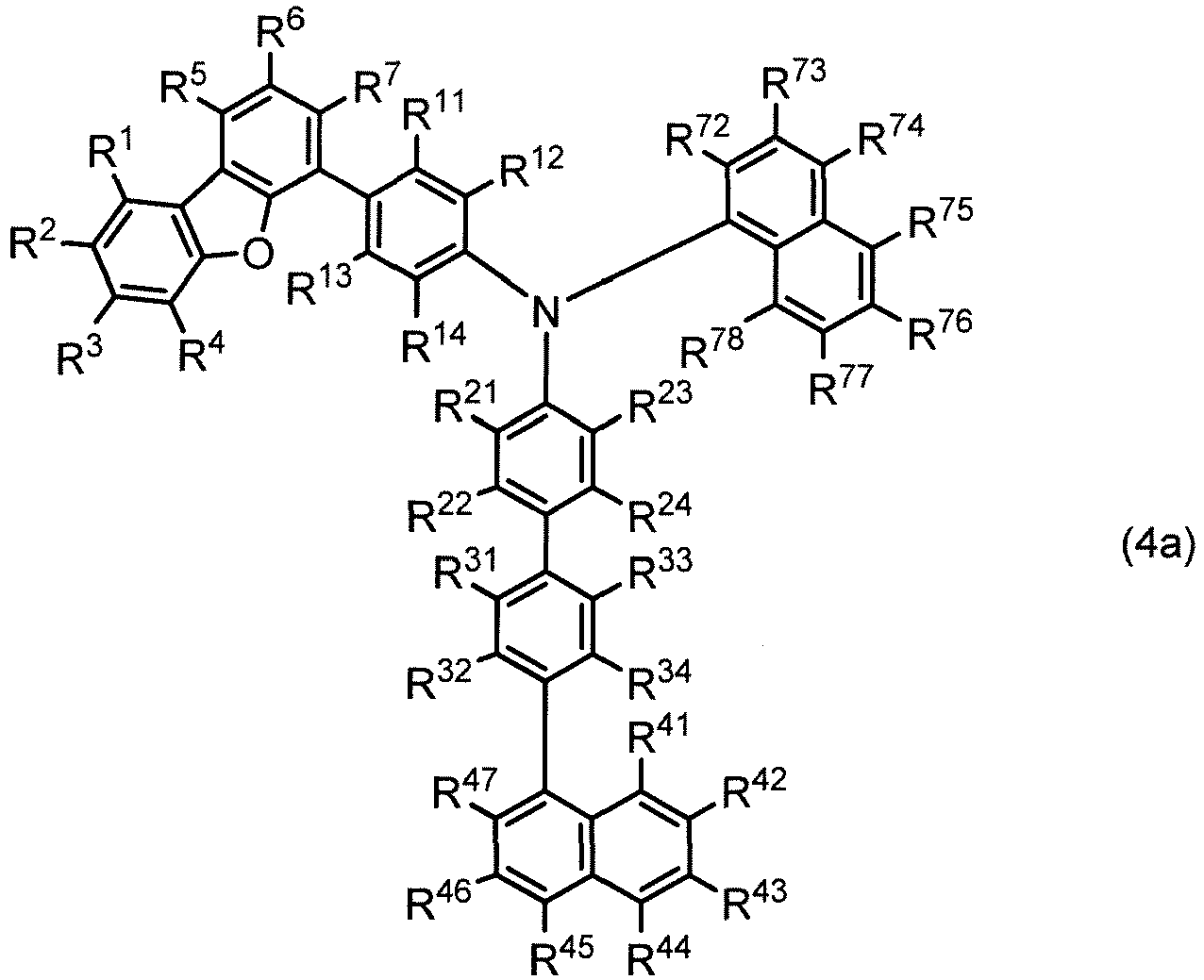
- Formula (4) is represented by formula (4a) or (4b), preferably represented by formula (4a):
- Formula (14) is represented by formula (14a) or (14b), preferably represented by formula (14a):
- Formula (5) is represented by any of formulae (5a) to (5e), preferably represented by formula (5b) or (5e):
- Formula (15) is represented by any of formulae (15a) to (15e), preferably represented by formula (5b) or (5e):
- halogen atom the alkyl group having 1 to 10 carbon atoms, and the cycloalkyl group having 3 to 6 ring carbon atoms are defined as follows, unless otherwise noted.
- the halogen atom is preferably an iodine atom, a bromine atom, a chlorine atom, or a fluorine atom, with a chlorine atom and a fluorine atom being preferred.
- the alkyl group having 1 to 10 carbon atoms is preferably an alkyl group having 1 to 6 carbon atoms, and more preferably an alkyl group having 1 to 4 carbon atoms.
- Examples thereof include a methyl group, an ethyl group a n-propyl group, a sec-propyl group, an isopropyl group, a n-butyl group, a sec-butyl group, an isobutyl group, and a t-butyl group, with a methyl group, an ethyl group, an isopropyl group, an isobutyl group, and a t-butyl group being preferred, a methyl group, an ethyl group, an isopropyl group, and a t-butyl group being more preferred, and a methyl group and a t-butyl group being still more preferred.
- the cycloalkyl group having 3 to 6 ring carbon atoms is preferably a cycloalkyl group having 5 or 6 ring carbon atoms.
- Examples thereof include a cyclopropyl group, a cyclobutyl group, a cyclopentyl group, and a cyclohexyl group, with a cyclopentyl group and a cyclohexyl group being preferred.
- Ar is a substituted or unsubstituted phenyl group, a substituted or unsubstituted biphenylyl group, a substituted or unsubstituted naphthyl group, or a substituted or unsubstituted phenanthryl group.
- the biphenylyl group includes an o-biphenylyl group, a m-biphenylyl group, and a p-biphenylyl group;
- the naphthyl group includes a 1-naphthyl group and 2-naphthyl group;
- the phenanthryl group includes a 1-phenanthryl group, a 2-phenanthryl group, a 3-phenanthryl group, a 4-phenanthryl group, and a 9-phenanthryl group.
- the biphenylyl group is preferably an o-biphenylyl group or a p-biphenylyl group
- the naphthyl group is preferably a 1-naphthyl group
- the phenanthryl group is preferably a 2-phenanthryl group or a 9-phenanthryl group.
- Ar is preferably an unsubstituted phenyl group, an unsubstituted biphenylyl group, an unsubstituted naphthyl group, or an unsubstituted phenanthryl group.
- the optional substituent for the phenyl group, the biphenylyl group, the naphthyl group, and the phenanthryl group is independently selected from a halogen atom, an alkyl group having 1 to 10 carbon atoms, and a cycloalkyl group having 3 to 6 ring carbon atoms.
- the details of the halogen atom, the alkyl group having 1 to 10 carbon atoms, and the cycloalkyl group having 3 to 6 ring carbon atoms are as described above.
- the phenyl group, the biphenylyl group, the naphthyl group, or the phenanthryl group has adjacent two optional substituent, the adjacent two optional substituents are not bonded to each other thereby failing to form a ring structure.
- R 1 to R 7 are each independently a hydrogen atom, a halogen atom, an alkyl group having 1 to 10 carbon atoms, or a cycloalkyl group having 3 to 6 ring carbon atoms.
- the details of the halogen atom, the alkyl group having 1 to 10 carbon atoms, and the cycloalkyl group having 3 to 6 ring carbon atoms are as described above.
- R 1 to R 7 are preferably all hydrogen atoms.
- R 11 to R 14 are each independently a hydrogen atom, a halogen atom, an alkyl group having 1 to 10 carbon atoms, or a cycloalkyl group having 3 to 6 ring carbon atoms.
- the details of the halogen atom, the alkyl group having 1 to 10 carbon atoms, and the cycloalkyl group having 3 to 6 ring carbon atoms are as described above.
- R 11 to R 14 are preferably all hydrogen atoms.
- R 21 to R 24 are each independently a hydrogen atom, a halogen atom, an alkyl group having 1 to 10 carbon atoms, or a cycloalkyl group having 3 to 6 ring carbon atoms.
- the details of the halogen atom, the alkyl group having 1 to 10 carbon atoms, and the cycloalkyl group having 3 to 6 ring carbon atoms are as described above.
- R 21 to R 24 are preferably all hydrogen atoms.
- R 31 to R 34 are each independently a hydrogen atom, a halogen atom, an alkyl group having 1 to 10 carbon atoms, or a cycloalkyl group having 3 to 6 ring carbon atoms.
- the details of the halogen atom, the alkyl group having 1 to 10 carbon atoms, and the cycloalkyl group having 3 to 6 ring carbon atoms are as described above.
- R 31 to R 34 are preferably all hydrogen atoms.
- R 41 to R 48 are each independently a hydrogen atom, a halogen atom, an alkyl group having 1 to 10 carbon atoms, or a cycloalkyl group having 3 to 6 ring carbon atoms, provided that one of R 47 and R 48 is a single bond bonded to *1.
- the details of the halogen atom, the alkyl group having 1 to 10 carbon atoms, and the cycloalkyl group having 3 to 6 ring carbon atoms are as described above.
- R 41 to R 48 not the single bond bonded to *1 are preferably all hydrogen atoms.
- R 51 to R 55 are each independently a hydrogen atom, a halogen atom, an alkyl group having 1 to 10 carbon atoms, or a cycloalkyl group having 3 to 6 ring carbon atoms.
- the details of the halogen atom, the alkyl group having 1 to 10 carbon atoms, and the cycloalkyl group having 3 to 6 ring carbon atoms are as described above.
- R 1 to R 7 , R 11 to R 14 , R 21 to R 24 , R 31 to R 34 , and R 41 to R 48 are as defined in formula (A), and adjacent two selected from R 51 to R 55 are not bonded to each other thereby failing to form a ring structure.
- R 51 to R 55 are preferably all hydrogen atoms.
- one selected from R 61 to R 65 is a single bond bonded to *a.
- R 61 to R 65 not the single bond bonded to *a and R 66 to R 70 are each independently a hydrogen atom, a halogen atom, an alkyl group having 1 to 10 carbon atoms, or a cycloalkyl group having 3 to 6 ring carbon atoms.
- the details of the halogen atom, the alkyl group having 1 to 10 carbon atoms, and the cycloalkyl group having 3 to 6 ring carbon atoms are as described above.
- R 1 to R 7 , R 11 to R 14 , R 21 to R 24 , R 31 to R 34 , and R 41 to R 48 are as defined in formula (A), and adjacent two selected from R 61 to R 65 not the single bond bonded to *a and R 66 to R 70 are not bonded to each other thereby failing to form a ring structure.
- R 61 to R 65 not the single bond bonded to *a and R 66 to R 70 are preferably all hydrogen atoms.
- one selected from R 71 and R 72 is a single bond bonded to *b.
- R 71 or R 72 not the single bond bonded to *b and R 73 to R 78 are each independently a hydrogen atom, a halogen atom, an alkyl group having 1 to 10 carbon atoms, or a cycloalkyl group having 3 to 6 ring carbon atoms.
- the details of the halogen atom, the alkyl group having 1 to 10 carbon atoms, and the cycloalkyl group having 3 to 6 ring carbon atoms are as described above.
- R 1 to R 7 , R 11 to R 14 , R 21 to R 24 , R 31 to R 34 , and R 41 to R 48 are as defined in formula (A), and adjacent two selected from R 71 or R 72 not the single bond bonded to *b and R 73 to R 78 are not bonded to each other thereby failing to form a ring structure.
- R 71 or R 72 not the single bond bonded to *b and R 73 to R 78 are preferably all hydrogen atoms.
- R 81 to R 90 not the single bond bonded to *c are each independently a hydrogen atom, a halogen atom, an alkyl group having 1 to 10 carbon atoms, or a cycloalkyl group having 3 to 6 ring carbon atoms.
- the details of the halogen atom, the alkyl group having 1 to 10 carbon atoms, and the cycloalkyl group having 3 to 6 ring carbon atoms are as described above.
- R 1 to R 7 , R 11 to R 14 , R 21 to R 24 , R 31 to R 34 , and R 41 to R 48 are as defined in formula (A), and adjacent two selected from R 81 to R 90 not the single bond bonded to *c are not bonded to each other thereby failing to form a ring structure.
- R 81 to R 90 not the single bond bonded to *c are preferably all hydrogen atoms.
- the inventive compound is preferably represented by any of the following formulae:
- the inventive compound is preferably represented by any of the following formulae:
- the "hydrogen atom” referred herein includes a light hydrogen (protium), a heavy hydrogen (deuterium), and tritium. Therefore, the inventive compound may include a naturally occurring heavy hydrogen atom.
- a heavy hydrogen atom may be intentionally introduced into the inventive compound by using a deuterated compound as a part or whole of the raw materials.
- the inventive compound comprises at least one heavy hydrogen atom. Therefore, the inventive compound may be a compound that is represented by any of formula (A) and preferred formulae thereof, wherein at one of the hydrogen atoms included in the compound is a heavy hydrogen atom.
- At least one hydrogen atom selected from the hydrogen atoms in the phenyl group, the biphenylyl group, the naphthyl group, or the phenanthryl group for Ar; the hydrogen atom(s) represented by any of R 1 to R 7 ; the hydrogen atom(s) represented by any of R 11 to R 14 ; the hydrogen atom(s) represented by any of R 21 to R 24 ; the hydrogen atom(s) represented by any of R 31 to R 34 ; and the hydrogen atom(s) represented by any of R 41 to R 48 not the single bond bonded to *1 may be a heavy hydrogen atom.
- the deuteration rate of the deuterated compound depends on the deuteration rate of the raw material to be used. It is generally difficult to use the raw materials each having a deuteration rate of 100%. Therefore, the deuteration rate of the inventive compound is less than 100% and 1% or more, preferably 3% or more, more preferably 5% or more, and still more preferably 10% or more.
- the inventive compound may be a mixture of a deuterated compound and a non-deuterated compound or a mixture of two or more compounds having different deuteration rates.
- the deuteration rate of such a mixture (the ratio of the number of heavy hydrogen atoms to the total number of hydrogen atoms each in the mixture) is 1% or more, preferably 3% or more, more preferably 5% or more, and still more preferably 10% or more, and less than 100%.
- At least one hydrogen atom selected from the hydrogen atoms in the phenyl group, the biphenylyl group, the naphthyl group, or the phenanthryl group for Ar may be a heavy hydrogen atom.
- the deuteration rate (the ratio of the number of heavy hydrogen atoms to the total number of hydrogen atoms each in Ar) is 1% or more, preferably 3% or more, more preferably 5% or more, and still more preferably 10% or more, and less than 100%.
- At least one hydrogen atom selected from the hydrogen atom(s) represented by any of R 1 to R 7 may be a heavy hydrogen atom.
- the deuteration rate (the ratio of the number of heavy hydrogen atoms to the total number of hydrogen atoms each represented by R 1 to R 7 ) is 1% or more, preferably 3% or more, more preferably 5% or more, and still more preferably 10% or more, and less than 100%.
- At least one hydrogen atom selected from the hydrogen atom(s) represented by any of R 11 to R 14 may be a heavy hydrogen atom.
- the deuteration rate (the ratio of the number of heavy hydrogen atoms to the total number of hydrogen atoms each represented by R 11 to R 14 ) is 1% or more, preferably 3% or more, more preferably 5% or more, and still more preferably 10% or more, and less than 100%.
- At least one hydrogen atom selected from the hydrogen atom(s) represented by any of R 21 to R 24 may be a heavy hydrogen atom.
- the deuteration rate (the ratio of the number of heavy hydrogen atoms to the total number of hydrogen atoms each represented by R 21 to R 24 ) is 1% or more, preferably 3% or more, more preferably 5% or more, and still more preferably 10% or more, and less than 100%.
- At least one hydrogen atom selected from the hydrogen atom(s) represented by any of R 31 to R 34 may be a heavy hydrogen atom.
- the deuteration rate (the ratio of the number of heavy hydrogen atoms to the total number of hydrogen atoms each represented by R 31 to R 34 ) is 1% or more, preferably 3% or more, more preferably 5% or more, and still more preferably 10% or more, and less than 100%.
- At least one hydrogen atom selected from the hydrogen atom(s) represented by any of R 41 to R 48 not the single bond bonded to *1 may be a heavy hydrogen atom.
- the deuteration rate (the ratio of the number of heavy hydrogen atoms to the total number of hydrogen atoms each represented by R 41 to R 48 not the single bond bonded to *1) is 1% or more, preferably 3% or more, more preferably 5% or more, and still more preferably 10% or more, and less than 100%.
- D in the following examples means a heavy hydrogen atom.
- the material for organic electroluminescence devices comprises the inventive compound.
- the content of the inventive compound in the material for organic electroluminescence devices is, for example, 1% by mass or more (inclusive of 100%), preferably 10% by mass or more (inclusive of 100%), more preferably 50% by mass or more (inclusive of 100%), still more preferably 80% by mass or more (inclusive of 100%), and particularly preferably 90% by mass or more (inclusive of 100%).
- the material for organic electroluminescence devices is useful for the production of an organic EL device.
- the organic electroluminescence device of the invention comprises an anode, a cathode, and an organic layer disposed between the anode and the cathode.
- the organic layer comprises a light emitting layer and at least one layer of the organic layer comprises the inventive compound.
- Examples of the organic layer which comprises the inventive compound include a hole transporting region formed between an anode and a light emitting layer, such as a hole transporting layer, a hole injecting layer, an electron blocking layer, and an exciton blocking layer, a light emitting layer, a space layer, and an electron transporting region formed between a cathode and a light emitting layer, such as an electron transporting layer, an electron injecting layer, and a hole blocking layer, although not limited thereto.
- the inventive compound is used for the production of a fluorescent or phosphorescent EL device preferably as a material for a hole transporting region or a light emitting layer, more preferably as a material for a hole transporting region, still more preferably as a material for a hole transporting layer, an electron blocking layer or an exciton blocking layer, and particularly preferably an electron blocking layer or an exciton blocking layer.
- the organic EL device of the invention may be any of a fluorescent or phosphorescent single color emitting device, a white-emitting device of fluorescent-phosphorescent hybrid type, a simple-type emitting device having a single emission unit, and a tandem emitting device having two or more emission units, with a fluorescent device being preferred.
- the "emission unit” referred to herein is the smallest unit for emitting light by the recombination of injected holes and injected electrons, which comprises an organic layer, wherein at least one layer is a light emitting layer.
- the emission unit may be a multi-layered structure comprising two or more layers selected from a phosphorescent light emitting layer and a fluorescent light emitting layer.
- a space layer may be disposed between the light emitting layers to prevent the diffusion of excitons generated in the phosphorescent light emitting layer into the fluorescent light emitting layer.
- Representative layered structures of the simple-type emission unit are shown below, wherein the layers in parentheses are optional:
- the emission colors of phosphorescent emitting layers or fluorescent emitting layers may be different.
- the emission unit (f) may be (Hole injecting layer)/Hole transporting layer/First phosphorescent emitting layer (red emission)/Second phosphorescent emitting layer (green emission)/Space layer/Fluorescent emitting layer (blue emission)/Electron transporting layer.
- An electron blocking layer may be disposed between each light emitting layer and the hole transporting layer or between each light emitting layer and the space layer, if necessary.
- a hole blocking layer may be disposed between each light emitting layer and the electron transporting layer, if necessary.
- the layered structure of the first emission unit and the second emission unit may be selected from those described above with respect to the emission unit.
- the intermediate layer is also called an intermediate electrode, an intermediate conductive layer, a charge generation layer, an electron withdrawing layer, a connecting layer, or an intermediate insulating layer.
- the intermediate layer supplies electrons to the first emission unit and holes to the second emission unit and may be formed by known materials.
- Fig. 1 is a schematic illustration showing the structure of an example of the organic EL device of the invention, wherein the organic EL device 1 comprises a substrate 2, an anode 3, a cathode 4, and an emission unit 10 disposed between the anode 3 and the cathode 4.
- the emission unit 10 comprises a light emitting layer 5.
- a hole transporting region 6 (for example, a hole injecting layer or a hole transporting layer) is disposed between the light emitting layer 5 and the anode 3, and an electron transporting region 7 (for example, an electron injecting layer or an electron transporting layer) is disposed between the light emitting layer 5 and the cathode 4.
- An electron blocking layer (not shown) may be disposed on the anode 3 side of the light emitting layer 5, and a hole blocking layer (not shown) may be disposed on the cathode 4 side of the light emitting layer 5. With these blocking layers, electrons and holes are confined in the light emitting layer 5 to increase the exciton generation in the light emitting layer 5.
- Fig. 2 is a schematic illustration showing the structure of another example of the organic EL device, wherein the organic EL device 11 comprises a substrate 2, an anode 3, a cathode 4, and an emission unit 20 disposed between the anode 3 and the cathode 4.
- the emission unit 20 comprises a light emitting layer 4.
- the hole transporting region disposed between the anode 3 and the light emitting layer 5 is formed by a first hole transporting layer 6a and a second hole transporting layer 6b.
- the electron transporting region disposed between the light emitting layer 5 and the cathode 4 is formed by a first electron transporting layer 7a and a second electron transporting layer 7b.
- a host is referred to as a fluorescent host when combinedly used with a fluorescent dopant (fluorescent emitting material) and as a phosphorescent host when combinedly used with a phosphorescent dopant (phosphorescent emitting material). Therefore, the fluorescent host and the phosphorescent host are not distinguished from each other merely by the difference in their molecular structures.
- the term "phosphorescent host” means a material for constituting a phosphorescent emitting layer containing a phosphorescent dopant and does not mean a material that cannot be used as a material for a fluorescent emitting layer. The same applies to the fluorescent host.
- the substrate is a support for the emitting device and made of, for example, glass, quartz, and plastics.
- the substrate may be a flexible substrate, for example, a plastic substrate made of polycarbonate, polyarylate, polyether sulfone, polypropylene, polyester, polyvinyl fluoride, or polyvinyl chloride.
- An inorganic deposition film is also usable.
- the anode is formed on the substrate preferably from a metal, an alloy, an electrically conductive compound, and a mixture thereof, each having a large work function, for example, 4.0 eV or more.
- the material for the anode include indium oxide-tin oxide (ITO: indium tin oxide), indium oxide-tin oxide doped with silicon or silicon oxide, indium oxide-zinc oxide, indium oxide doped with tungsten oxide and zinc oxide, and graphene.
- gold Au
- platinum Pt
- nickel Ni
- tungsten W
- Cr chromium
- Mo molybdenum
- iron Fe
- Co cobalt
- Cu copper
- palladium Pd
- titanium Ti
- a nitride of the above metal for example, titanium nitride
- These anode materials are made into a film generally by a sputtering method.
- a film of indium oxide-zinc oxide is formed by sputtering an indium oxide target doped with 1 to 10 wt% of zinc oxide
- a film of indium oxide doped with tungsten oxide and zinc oxide is formed by sputtering an indium oxide target doped with 0.5 to 5 wt% of tungsten oxide and 0.1 to 1 wt% of zinc oxide.
- a vacuum vapor deposition method, a coating method, an inkjet method, and a spin coating method are usable.
- a hole injecting layer to be optionally formed in contact with the anode is formed from a material which is capable of easily injecting holes independently of the work function of the anode. Therefore, the anode can be formed by a material generally known as an electrode material, for example, a metal, an alloy, an electroconductive compound, a mixture thereof, and a group 1 element and a group 2 element of the periodic table.
- an electrode material for example, a metal, an alloy, an electroconductive compound, a mixture thereof, and a group 1 element and a group 2 element of the periodic table.
- a material having a small work function belonging to a group 1 or a group 2 of the periodic table for example, an alkali metal, such as lithium (Li) and cesium (Cs), an alkaline earth metal, such as magnesium (Mg), calcium (Ca), and strontium (Sr), and an alloy thereof, such as MgAg and AlLi, are also usable as an anode material.
- an alkali metal such as lithium (Li) and cesium (Cs)
- an alkaline earth metal such as magnesium (Mg), calcium (Ca), and strontium (Sr)
- an alloy thereof such as MgAg and AlLi
- a rare earth metal such as europium and ytterbium
- the alkali metal, the alkaline earth metal, and the alloy thereof is made into the anode by a vacuum vapor deposition or a sputtering method. When a silver paste is used, a coating method and an inkjet method are usable.
- the hole injecting layer comprises a material having a high hole injecting ability (hole injecting material) and formed between an anode and a light emitting layer or between an anode and a hole transporting layer, if present.
- Examples of the hole injecting material include molybdenum oxide, titanium oxide, vanadium oxide, rhenium oxide, ruthenium oxide, chromium oxide, zirconium oxide, hafnium oxide, tantalum oxide, silver oxide, tungsten oxide, and manganese oxide.
- the following low molecular aromatic amine compound is also usable as the hole injecting layer material: 4,4',4"-tris(N,N-diphenylamino)triphenylamine (TDATA), 4,4',4"-tris[N-(3-methylphenyl)-N-phenylamino]triphenylamine (MTDATA), 4,4'-bis[N-(4-diphenylaminophenyl)-N-phenylamino]biphenyl (DPAB), 4,4'-bis(N- ⁇ 4-[N'-(3-methylphenyl)-N'-phenylamino]phenyl ⁇ -N-phenylamino)biphenyl (DNTPD), 1,3,5-tris[N-(4-diphenylaminophenyl)-N-phenylamino]benzene (DPA3B), 3-[N-(9-phenylcarbazole-3-yl)-N-phenylamino]-9-phen
- a macromolecular compound such as an oligomer, a dendrimer, a polymer, is also usable as the hole injecting layer material.
- Examples thereof include poly(N-vinylcarbazole) (PVK), poly(4-vinyltriphenylamine) (PVTPA), poly[N-(4- ⁇ N'-[4-(4-diphenylamino)phenyl]phenyl-N'-phenylamino ⁇ phenyl)methacrylamide] (PTPDMA), and poly[N,N'-bis(4-butylphenyl)-N,N'-bis(phenyl)benzidine] (Poly-TPD).
- PVK poly(N-vinylcarbazole)
- PVTPA poly(4-vinyltriphenylamine)
- PTPDMA poly[N-(4- ⁇ N'-[4-(4-diphenylamino)phenyl]phenyl-N'-phenylamino
- a macromolecular compound doped with an acid such as poly(3,4-ethylenedioxythiophene)/poly(styrenesulfonic acid) (PEDOT/PSS) and polyaniline/poly(styrenesulfonic acid) (PAni/PSS), is also usable.
- an acid such as poly(3,4-ethylenedioxythiophene)/poly(styrenesulfonic acid) (PEDOT/PSS) and polyaniline/poly(styrenesulfonic acid) (PAni/PSS)
- an acceptor material such as a hexaazatriphenylene (HAT) compound represented by formula (K), is preferably used: wherein:
- R 27 examples include a methyl group, an ethyl group, a n-propyl group, an isopropyl group, a n-butyl group, an isobutyl group, a t-butyl group, a cyclopentyl group, and a cyclohexyl group.
- the hole transporting layer comprises a material having a high hole transporting ability (hole transporting material) and formed between an anode and a light emitting layer or between a hole injecting layer, if present, and a light emitting layer.
- the inventive compound is preferably used in a hole transporting layer alone or in combination with the compound described below.
- the hole transporting layer may be a single layer or a multi-layer of two or more layers.
- the hole transporting layer may be a two-layered structure comprising a first hole transporting layer (anode side) and a second hole transporting layer (cathode side).
- a hole transporting layer of a single-layered structure is preferably in contact with a light emitting layer and a hole transporting layer in a multi-layered structure which is closest to a cathode, for example, the second hole transporting layer in the two-layered structure mentioned above, is preferably in contact with a light emitting layer.
- an electron blocking layer may be disposed between the light emitting layer and the hole transporting layer of the single-layered structure or between the light emitting layer and the hole transporting layer in the multi-layered structure which is closest to the light emitting layer.
- the inventive compound may be included in one or both of the first hole transporting layer and the second hole transporting layer.
- the inventive compound is preferably used in the first hole transporting layer.
- the inventive compound is preferably used in the second hole transporting layer.
- the inventive compound is preferably used in both the first hole transporting layer and the second hole transporting layer.
- the inventive compound used in one or both of the first hole transporting layer and the second hole transporting layer is preferably a light-hydrogen analogue in view of production cost.
- the light-hydrogen analogue means the inventive compound wherein all the hydrogen atoms are light hydrogen atoms.
- the present invention includes an organic EL device comprising the inventive compound in one or both of the first hole transporting layer and the second hole transporting layer, wherein the inventive compound is substantially a light-hydrogen analogue.
- inventive compound is substantially a light-hydrogen analogue used herein means that the content of the light-hydrogen analogue in the total amount of the inventive compound is 90 mol % or more, preferably 95 mol % or more, and still more preferably 99 mol % or, each inclusive of 100%.
- Examples of the hole transporting material other than the inventive compound includes an aromatic amine compound, a carbazole derivative, and an anthracene derivative.
- aromatic amine compound examples include 4,4'-bis[N-(1-naphthyl)-N-phenylamino]biphenyl (NPB), N,N'-bis(3-methylphenyl)-N,N'-diphenyl-[1,1'-biphenyl]-4,4'-diamine (TPD), 4-phenyl-4'-(9-phenylfluorene-9-yl)triphenylamine (BAFLP), 4,4'-bis[N-(9,9-dimethylfluorene-2-yl)-N-phenylamino]biphenyl (DFLDPBi), 4,4',4"-tris(N,N-diphenylamino)triphenylamine (TDATA), 4,4',4"-tris[N-(3-methylphenyl)-N-phenylamino]triphenylamine (MTDATA), and 4,4'-bis[N-(spiro-9,9'-b
- carbazole derivative examples include 4,4'-di(9-carbazolyl)biphenyl (CBP), 9-[4-(9-carbazolyl)phenyl]-10-phenylanthracene (CzPA), and 9-phenyl-3-[4-(10-phenyl-9-anthryl)phenyl]-9H-carbazole (PCzPA).
- anthracene derivative examples include 2-t-butyl-9,10-di(2-naphthyl)anthracene (t-BuDNA), 9,10-di(2-naphthyl)anthracene (DNA), and 9,10-diphenylanthracene (DPAnth).
- a macromolecular compound such as poly(N-vinylcarbazole) (PVK) and poly(4-vinyltriphenylamine) (PVTPA) are usable.
- PVK poly(N-vinylcarbazole)
- PVTPA poly(4-vinyltriphenylamine)
- the light emitting layer comprises a highly light-emitting material (dopant material) and may be formed from a various kind of materials.
- a fluorescent emitting material and a phosphorescent emitting material are usable as the dopant material.
- the fluorescent emitting material is a compound capable of emitting light from a singlet excited state
- the phosphorescent emitting material is a compound capable of emitting light from a triplet excited state.
- blue fluorescent emitting material usable in the light emitting layer examples include a pyrene derivative, a styrylamine derivative, a chrysene derivative, a fluoranthene derivative, a fluorene derivative, a diamine derivative, and a triarylamine derivative, such as N,N'-bis[4-(9H-carbazole-9-yl)phenyl]-N,N'-diphenylstilbene-4,4'-diamine (YGA2S), 4-(9H-carbazole-9-yl)-4'-(10-phenyl-9-anthryl)triphenylamine (YGAPA), and 4-(10-phenyl-9-anthryl)-4'-(9-phenyl-9H-carbazole-3-yl)triphenylamine (PCBAPA).
- a pyrene derivative such as N,N'-bis[4-(9H-carbazole-9-yl)phenyl]-N,N
- green fluorescent emitting material usable in the light emitting layer examples include an aromatic amine derivative, such as N-(9,10-diphenyl-2-anthryl)-N,9-diphenyl-9H-carbazole-3-amine (2PCAPA), N-[9,10-bis(1,1'-biphenyl-2-yl)-2-anthryl]-N,9-diphenyl-9H-carbazole-3-amine (2PCABPhA), N-(9,10-diphenyl-2-anthryl)-N,N',N'-triphenyl-1,4-phenylenediamine (2DPAPA), N-[9,10-bis(1,1'-biphenyl-2-yl)-2-anthryl]-N,N',N'-triphenyl-1,4-phenylenediamine (2DPABPhA), N-[9,10-bis(1,1'-biphenyl-2-yl)]-N-[4-(9H
- red fluorescent emitting material usable in the light emitting layer examples include a tetracene derivative and a diamine derivative, such as N,N,N',N'-tetrakis(4-methylphenyl)tetracene-5,11-diamine (p-mPhTD) and 7,14-diphenyl-N,N,N',N'-tetrakis(4-methylphenyl)acenaphtho[1,2-a]fluoranthene-3,10-diamine (p-mPhAFD).
- a tetracene derivative and a diamine derivative such as N,N,N',N'-tetrakis(4-methylphenyl)tetracene-5,11-diamine (p-mPhTD) and 7,14-diphenyl-N,N,N',N'-tetrakis(4-methylphenyl)acenaphtho[1,2-a]fluoranthene-3
- blue phosphorescent emitting material usable in the light emitting layer include a metal complex, such as an iridium complex, an osmium complex, and a platinum complex.
- a metal complex such as an iridium complex, an osmium complex, and a platinum complex.
- examples thereof include bis[2-(4',6'-difluorophenyl)pyridinato-N,C2']iridium(III) tetrakis(1-pyrazolyl)borato (FIr 6 ), bis[2-(4',6'-difluorophenyl)pyridinato-N,C2']iridium(III) picolinato (FIrpic), bis[2-(3',5'-bistrifluoromethylphenyl)pyridinato-N,C2']iridium(III) picolinato (Ir(CF 3 ppy) 2 (pic)), and bis[2-(4',6'-di
- green phosphorescent emitting material usable in the light emitting layer examples include an iridium complex, such as tris(2-phenylpyridinato-N,C2')iridium(III) (Ir(ppy) 3 ), bis(2-phenylpyridinato-N,C2')iridium(III) acetylacetonato (Ir(ppy) 2 (acac)), bis(1,2-diphenyl-1H-benzimidazolato)iridium(III) acetylacetonato (Ir(pbi) 2 (acac)), and bis(benzo[h]quinolinato)iridium(III) acetylacetonato (Ir(bzq) 2 (acac)).
- an iridium complex such as tris(2-phenylpyridinato-N,C2')iridium(III) (Ir(ppy) 3 ), bis(2-phenylpyridinato-
- red phosphorescent emitting material usable in the light emitting layer examples include a metal complex, such as an iridium complex, a platinum complex, a terbium complex, and a europium complex.
- a metal complex such as an iridium complex, a platinum complex, a terbium complex, and a europium complex.
- organometallic complex such as bis[2-(2'-benzo[4,5- ⁇ ]thienyl)pyridinato-N,C3']iridium(III) acetylacetonato (Ir(btp) 2 (acac)), bis(1-phenylisoquinolinato-N,C2')iridium(III) acetylacetonato (Ir(piq) 2 (acac)), (acetylacetonato)bis[2,3-bis(4-fluorophenyl)quinoxalinato]iridium(III) (Ir(Fdpq
- a rare earth metal complex such as tris(acetylacetonato) (monophenanthroline)terbium(III) (Tb(acac) 3 (Phen)), tris(1,3-diphenyl-1,3-propanedionato)(monophenanthroline)europium(III) (Eu(DBM) 3 (Phen)), and tris[1-(2-thenoyl)-3,3,3-trifluoroacetonato](monophenanthroline)europium(III) (Eu(TTA) 3 (Phen)), emits light from the rare earth metal ion (electron transition between different multiple states), and therefore, usable as a phosphorescent emitting material.
- the light emitting layer may be a layer wherein the above dopant material is dispersed in another material (host material).
- the host material preferably has a lowest unoccupied molecular orbital level (LUMO level) higher than that of the dopant material and a highest occupied molecular orbital level (HOMO level) lower than that of the dopant material.
- LUMO level lowest unoccupied molecular orbital level
- HOMO level highest occupied molecular orbital level
- the host material other the compound (1) may include, for example,
- Examples thereof include:
- the host material may be used alone or in combination of two or more.
- the following anthracene compound is preferably used as a host material for a blue fluorescent device.
- the electron transporting layer comprises a material having a high electron transporting ability (electron transporting material) and formed between a light emitting layer and a cathode or between a light emitting layer and an electron injecting layer, if present.
- the electron transporting layer may be a single layer or a multi-layer of two or more layers.
- the electron transporting layer may be a two-layered structure comprising a first electron transporting layer (anode side) and a second electron transporting layer (cathode side).
- an electron transporting layer of a single-layered structure is preferably in contact with a light emitting layer and an electron transporting layer in a multi-layered structure which is closest to an anode, for example, the first electron transporting layer in the two-layered structure mentioned above, is preferably in contact with a light emitting layer.
- an hole blocking layer mentioned below may be disposed between the light emitting layer and the electron transporting layer of the single-layered structure or between the light emitting layer and the electron transporting layer in the multi-layered structure which is closest to the light emitting layer.
- the electron transporting layer may be formed, for example, by
- metal complex examples include tris(8-quinolinolato)aluminum (III) (Alq), tris(4-methyl-8-quinolinolato)aluminum (Almq 3 ), bis(10-hydroxybenzo[h]quinolinato)beryllium (BeBq 2 ), bis(2-methyl-8-quinolinato)(4-phenylphenolato)aluminum (III) (BAlq), bis(8-quinolinato)zinc(II) (Znq), bis[2-(2-benzoxazolyl)phenolato]zinc(II) (ZnPBO), and bis[2-(2-benzothiazolyl)phenolato]zinc(II) (ZnBTZ).
- heteroaromatic compound examples include 2-(4-biphenylyl)-5-(4-tert-butylphenyl)-1,3,4-oxadiazole (PBD), 1,3-bis[5-(p-tert-butylphenyl)-1,3,4-oxadiazole-2-yl]benzene (OXD-7), 3-(4-tert-butylphenyl)-4-phenyl-5-(4-biphenylyl)-1,2,4-triazole (TAZ), 3-(4-tert-butylphenyl)-4-(4-ethylphenyl)-5-(4-biphenylyl)-1,2,4-triazole (p-EtTAZ), bathophenanthroline (BPhen), bathocuproine (BCP), and 4,4'-bis(5-methylbenzoxazole-2-yl)stilbene (BzOs).
- PBD 2-(4-biphenylyl)-5-(
- macromolecular compound examples include poly[(9,9-dihexylfluorene-2,7-diyl)-co-(pyridine-3,5-diyl)] (PF-Py), and poly[(9,9-dioctylfluorene-2,7-diyl)-co-(2,2'-bipyridine-6,6'-diyl)] (PF-BPy).
- the above compounds have an electron mobility of 10 -6 cm 2 /Vs or more. Materials other than those mentioned above are also usable in the electron transporting layer if their electron transporting ability is higher than their hole transporting ability.
- the electron injecting layer is a layer comprising a material having a high electron injecting ability, for example, an alkali metal, such as lithium (Li), cesium (Cs), an alkaline earth metal, such as magnesium (Mg), calcium (Ca), and strontium (Sr), a rare earth metal, such as europium (Eu) and ytterbium (Yb), and a compound of these metals, such as an alkali metal oxide, an alkali metal halide, an alkali metal-containing organic complex, an alkaline earth metal oxide, an alkaline earth metal halide, an alkaline earth metal-containing organic complex, a rare earth metal oxide, a rare earth metal halide, and a rare metal-containing organic complex. These compounds may be used in combination of two or more.
- an alkali metal such as lithium (Li), cesium (Cs)
- an alkaline earth metal such as magnesium (Mg), calcium (Ca), and strontium (Sr)
- an electron transporting material which is doped with an alkali metal, an alkaline earth metal or a compound thereof, for example, Alq doped with magnesium (Mg), is also usable. By using such a material, electrons are efficiently injected from the cathode.
- a composite material comprising an organic compound and an electron donor is also usable in the electron injecting layer.
- Such a composite material is excellent in the electron injecting ability and the electron transporting ability, because the organic compound receives electrons from the electron donor.
- the organic compound is preferably a compound excellent in transporting the received electrons. Examples thereof include the materials for the electron transporting layer mentioned above, such as the metal complex and the aromatic heterocyclic compound. Any compound capable of giving its electron to the organic compound is usable as the electron donor.
- Preferred examples thereof are an alkali metal, an alkaline earth metal, and a rare earth metal, such as lithium, cesium, magnesium, calcium, erbium, and ytterbium; an alkali metal oxide and an alkaline earth metal oxide, such as, lithium oxide, calcium oxide, and barium oxide; a Lewis base, such as magnesium oxide; and an organic compound, such as tetrathiafulvalene (TTF).
- a rare earth metal such as lithium, cesium, magnesium, calcium, erbium, and ytterbium
- an alkali metal oxide and an alkaline earth metal oxide such as, lithium oxide, calcium oxide, and barium oxide
- a Lewis base such as magnesium oxide
- an organic compound such as tetrathiafulvalene (TTF).
- the cathode is formed preferably from a metal, an alloy, an electrically conductive compound, or a mixture thereof, each having a small work function, for example, a work function of 3.8 eV or less.
- the material for the cathode include an element belonging to a group 1 or group 2 of the periodic table, i.e., an alkali metal, such as lithium (Li) and cesium (Cs), an alkaline earth metal, such as magnesium (Mg), calcium (Ca), and strontium (Sr), an alloy containing these metals (for example, MgAg and AlLi), a rare earth metal, such as europium (Eu) and ytterbium (Yb), and an alloy containing a rare earth metal.
- an alkali metal such as lithium (Li) and cesium (Cs)
- an alkaline earth metal such as magnesium (Mg), calcium (Ca), and strontium (Sr)
- an alloy containing these metals for example, Mg
- the alkali metal, the alkaline earth metal, and the alloy thereof is made into the cathode by a vacuum vapor deposition or a sputtering method.
- a coating method and an inkjet method are usable when a silver paste is used.
- the material for the cathode is selected irrespective of whether the work function is large or small and various electroconductive materials, such as Al, Ag, ITO, graphene, and indium oxide-tin oxide doped with silicon or silicon oxide, are usable. These electroconductive materials are made into films by a sputtering method, an inkjet method, and a spin coating method.
- an insulating thin film layer may be interposed between the pair of electrodes.
- Examples of the material for the insulating layer include aluminum oxide, lithium fluoride, lithium oxide, cesium fluoride, cesium oxide, magnesium oxide, magnesium fluoride, calcium oxide, calcium fluoride, aluminum nitride, titanium oxide, silicon oxide, germanium oxide, silicon nitride, boron nitride, molybdenum oxide, ruthenium oxide, and vanadium oxide. These materials may be used in combination or may be used in each layer of stacked layers.
- a space layer is disposed between the fluorescent emitting layer and the phosphorescent emitting layer to prevent the diffusion of excitons generated in the phosphorescent emitting layer to the fluorescent emitting layer or to control the carrier (charge) balance.
- the space layer may be disposed between two or more phosphorescent emitting layers.
- the space layer is disposed between the light emitting layers, a material combining the electron transporting ability and the hole transporting ability is preferably used for forming the space layer.
- the triplet energy of the material for the space layer is preferably 2.6 eV or more.
- the materials described with respect to the hole transporting layer are usable as the material for the space layer.
- a blocking layer such as an electron blocking layer, a hole blocking layer, and an exciton blocking layer, may be provided in the portion adjacent to the light emitting layer.
- the electron blocking layer is a layer which prevents the diffusion of electrons from the light emitting layer to the hole transporting layer.
- the hole blocking layer is a layer which prevents the diffusion of holes from the light emitting layer to the electron transporting layer.
- the exciton blocking layer prevents the diffusion of excitons generated in the light emitting layer to adjacent layers and has a function of confining the excitons in the light emitting layer.
- Each layer of the organic EL device is formed by a known method, such as a vapor deposition method and a coating method.
- each layer is formed by a known vapor deposition method, such as a vacuum vapor deposition method and a molecular beam evaporation method (MBE method), and a known coating method using a solution of a compound for forming a layer, such as a dipping method, a spin coating method, a casting method, a bar coating method, and a roll coating method.
- a known vapor deposition method such as a vacuum vapor deposition method and a molecular beam evaporation method (MBE method
- MBE method molecular beam evaporation method
- a known coating method using a solution of a compound for forming a layer such as a dipping method, a spin coating method, a casting method, a bar coating method, and a roll coating method.
- each layer is not particularly limited and preferably 5 nm to 10 ⁇ m, more preferably 10 nm to 0.2 ⁇ m, because an excessively small thickness may cause defects such as pin holes and an excessively large thickness may require a high driving voltage.
- the organic EL device can be used in an electronic device, for example, as display parts, such as organic EL panel module, display devices of television sets, mobile phones, personal computer, etc., and light emitting sources of lighting equipment and vehicle lighting equipment.
- display parts such as organic EL panel module, display devices of television sets, mobile phones, personal computer, etc., and light emitting sources of lighting equipment and vehicle lighting equipment.
- the comparative compound Ref-1 is described in Patent Literature 2 and the comparative compounds Ref-2, Ref-3, and Ref-4 are described in Patent Literature 1.
- Each organic EL device was produced in the following manner and evaluated for EL device performance.
- ITO transparent electrode anode (product of Geomatec Company) was ultrasonically cleaned in isopropyl alcohol for 5 min and then UV/ozone cleaned for 30 min.
- the thickness of ITO transparent electrode was 130 nm.
- the cleaned glass substrate having a transparent electrode line was mounted to a substrate holder of a vacuum vapor deposition apparatus.
- the compound HI-1 was vapor-deposited on the surface having the transparent electrode line so as to cover the transparent electrode to form a hole injecting layer with a thickness of 5 nm.
- the compound HT-1 was vapor-deposited to form a first hole transporting layer with a thickness of 80 nm.
- the compound Inv-1 was vapor-deposited to form a second hole transporting layer with a thickness of 10 nm.
- the compound BH-1 (host material) and the compound BD-1 (dopant material) were vapor co-deposited to form a light emitting layer with a thickness of 25 nm.
- the concentration of the compound BD-1 in the light emitting layer was 4.0% by mass.
- the compound ET-1 was vapor-deposited to form a first electron transporting layer with a thickness of 10 nm.
- the compound ET-2 was vapor-deposited to form a second electron transporting layer with a thickness of 15 nm, thereby forming a second electron transporting layer.
- LiF was vapor-deposited to form an electron injecting electrode (cathode) with a thickness of 1 nm.
- metallic Al was vapor-deposited on the electron injecting electrode to form a metallic cathode with a thickness of 80 nm.
- Each organic EL device was produced in the same manner as in Example 1 except for using each compound described in Table 1 as the second hole transporting layer material in place of the compound Inv-1.
- Each organic EL device was produced in the same manner as in Example 1 except for using each compound described in Table 1 as the second hole transporting layer material in place of compound Inv-1.
- the organic EL device thus produced was operated by a constant direct current at room temperature at a current density of 10 mA/cm 2 to measure the luminance by a luminance meter (spectroradiometer CS-1000 manufactured by Minolta). The external quantum efficiency (%) was determined by the results.
- the organic EL device comprising any of the compounds Inv-1 to Inv-5 and Inv-12 of formula (1) of the invention showed a high efficiency (high external quantum efficiency).
- the organic EL device comprising any of the compound Ref-1 described in Patent Literature 2 and any of the compounds Ref-2, Ref-3, and Ref-4 each described in Patent Literature 1 showed a poor efficiency (external quantum efficiency).
- the intermediate 1 (7 mmol, 3.8 g), 4-bromobiphenyl (7 mmol, 1.6 g), tris(dibenzylideneacetone)dipalladium(0) (0.14 mmol, 128 mg), tri-tert-butylphosphonium tetrafluoroborate (0.56 mmol, 162 mg), sodium tert-butoxide (9.8 mmol, 942 mg), and xylene (35 mL) were charged in a flask and refluxed for 4 h by stirring under heating.
Landscapes
- Chemical & Material Sciences (AREA)
- Physics & Mathematics (AREA)
- Organic Chemistry (AREA)
- Optics & Photonics (AREA)
- Spectroscopy & Molecular Physics (AREA)
- Engineering & Computer Science (AREA)
- Materials Engineering (AREA)
- Electroluminescent Light Sources (AREA)
- Furan Compounds (AREA)
Abstract

Description
- The present invention relates to compounds, materials for organic electroluminescence devices, organic electroluminescence devices, and electronic devices comprising the organic electroluminescence devices.
- An organic electroluminescence device ("organic EL device") is generally composed of an anode, a cathode, and an organic layer sandwiched between the anode and the cathode. When a voltage is applied between the electrodes, electrons are injected from the cathode and holes are injected from the anode into a light emitting region. The injected electrons recombine with the injected holes in the light emitting region to form excited states. When the excited states return to the ground state, the energy is released as light. Therefore, it is important for obtaining an organic EL device with a high efficiency to develop a compound that transports electrons or holes into the light emitting region efficiently and facilitates the recombination of electrons and holes.
-
Patent Literature 1 describes an aromatic amine derivative, wherein the nitrogen atom has a group comprising a dibenzofuran structure, a group comprising a terphenyl structure, and an aryl group. In the working examples, the aromatic amine derivative is used in a hole transporting layer. -
Patent Literature 2 describes an aromatic amine derivative having at least one group comprising a dibenzofuran structure and an aryl group on the nitrogen atom. In the working examples, the aromatic amine derivative is used in a hole transporting layer. -
- Patent Literature 1:
WO 2009/145016 - Patent Literature 2:
WO 2007/125714 - Various compounds for organic EL devices have been reported. However, compounds that further improve the performance of organic EL devices have been still demanded.
- The present invention has been made to solve the above problem and an object of the invention is to provide compounds further improving the performance of organic EL devices, organic EL devices having their performance further improved, and electronic devices comprising such organic EL devices.
- The inventors have extensively studied organic EL devices comprising the compounds described in
Patent Literatures Patent Literatures - In an aspect, the present invention provides a compound represented by formula (A) (hereinafter also referred to as "inventive compound"):

- Ar is a substituted or unsubstituted phenyl group, a substituted or unsubstituted biphenylyl group, a substituted or unsubstituted naphthyl group, or a substituted or unsubstituted phenanthryl group;
- R1 to R7 are each independently a hydrogen atom, a halogen atom, an alkyl group having 1 to 10 carbon atoms, or a cycloalkyl group having 3 to 6 ring carbon atoms;
- R11 to R14 are each independently a hydrogen atom, a halogen atom, an alkyl group having 1 to 10 carbon atoms, a cycloalkyl group having 3 to 6 ring carbon atoms;
- R21 to R24 are each independently a hydrogen atom, a halogen atom, an alkyl group having 1 to 10 carbon atoms, or a cycloalkyl group having 3 to 6 ring carbon atoms;
- R31 to R34 are each independently a hydrogen atom, a halogen atom, an alkyl group having 1 to 10 carbon atoms, or a cycloalkyl group having 3 to 6 ring carbon atoms;
- R41 to R48 are each independently a hydrogen atom, a halogen atom, an alkyl group having 1 to 10 carbon atoms, or a cycloalkyl group having 3 to 6 ring carbon atoms, provided that one of R47 and R48 is a single bond bonded to *1;
- the optional substituent for the phenyl group, the biphenylyl group, the naphthyl group, and the phenanthryl group is independently a halogen atom, an alkyl group having 1 to 10 carbon atoms, or a cycloalkyl group having 3 to 6 ring carbon atoms;
- adjacent two selected from R1 to R7, R11 to R14, R21 to R24, R31 to R34, and R41 to R48 not the single bond bonded to *1 are not bonded to each other thereby failing to form a ring structure; and
- if the phenyl group, the biphenylyl group, the naphthyl group, or the phenanthryl group has adjacent two optional substituents, the adjacent two optional substituents are not bonded to each other thereby failing to form a ring structure.
- In another aspect, the present invention provides a material for organic EL device comprising the inventive compound.
- In another aspect, the present invention provides an organic electroluminescence device comprising an anode, a cathode, and an organic layer disposed between the anode and the cathode, wherein the organic layer comprises a light emitting layer and at least one layer of the organic layer comprises the inventive compounds.
- In another aspect, the present invention provides an electronic device comprising the organic electroluminescence device.
- The organic EL device comprising the inventive compound exhibits a high efficiency while having a long lifetime.
-
-
Fig. 1 is a schematic view showing the layered structure of an organic EL device in an embodiment of the invention. -
Fig. 1 is a schematic view showing the layered structure of an organic EL device in another embodiment of the invention. - The definition of "hydrogen atom" used herein includes isotopes different in the neutron numbers, i.e., light hydrogen (protium), heavy hydrogen (deuterium), and tritium.
- The number of ring carbon atoms referred to herein means the number of the carbon atoms included in the atoms that form the ring itself of a compound in which a series of atoms are bonded to form a cyclic compound (for example, a monocyclic compound, a fused ring compound, a cross-linked compound, a carbocyclic compound, and a heterocyclic compound) and a compound in which two or more cyclic compounds are directly bonded (ring assembly compound). If the ring has a substituent, the carbon atom in the substituent is not included in the ring carbon atom. Unless otherwise noted, the same applies to the number of ring carbon atoms mentioned below.
- For example, a benzene ring has 6 ring carbon atoms, a naphthalene ring has 10 ring carbon atoms, a pyridinyl group has 5 ring carbon atoms, a furan ring has 4 ring carbon atoms, 9,9-diphenylfluorenyl group has 13 ring carbon atoms, and a 9,9'-spirobifluorenyl group has 25 ring carbon atoms.
- If a benzene ring has, for example, an alkyl substituent, the carbon atom in the alkyl substituent is not counted as the ring carbon atom of the benzene ring. Therefore, an alkyl-substituted benzene ring has 6 ring carbon atoms. If a naphthalene ring has, for example, an alkyl substituent, the carbon atom in the alkyl substituent is not counted as the ring carbon atom of the naphthalene ring. Therefore, an alkyl-substituted naphthalene ring has 10 ring carbon atoms.
- The number of ring atom referred to herein means the number of the atoms that form the ring itself of the cyclic compounds and the ring assembly compounds mentioned above. The hydrogen atom bonded to the ring atom and the atom in the substituent bonded to the ring atom are not counted as the ring atom. Unless otherwise noted, the same applies to the number of ring atoms mentioned below.
- For example, a pyridine ring has 6 ring atoms, a quinazoline ring has 10 ring atoms, and a furan ring has 5 ring atoms. The hydrogen atom and the atom in a substituent bonded to a pyridine ring are not counted as the ring atom. Therefore, a substituted pyridine ring has 6 ring atoms. The hydrogen atom and the atom in a substituent bonded to a quinazoline ring are not counted as the ring atom. Therefore, a substituted quinazoline ring has 10 ring atoms.
- The term of "XX to YY carbon atoms" referred to by "a substituted or unsubstituted group ZZ having XX to YY carbon atoms" used herein is the number of carbon atoms of the unsubstituted group ZZ and does not include any carbon atom in the substituent of the substituted group ZZ.
- The term of "XX to YY atoms" referred to by "a substituted or unsubstituted group ZZ having XX to YY atoms" used herein is the number of atoms of the unsubstituted group ZZ and does not include any atom in the substituent of the substituted group ZZ.
- The term of "unsubstituted group ZZ" referred to by "substituted or unsubstituted group ZZ" used herein means that no hydrogen atom in the group ZZ is substituted by a substituent.
- The term of "substituted group ZZ" referred to by "substituted or unsubstituted group ZZ" used herein means that at least one hydrogen atom in the group ZZ is substituted by a substituent. The term "group BB substituted by group AA" means that at least one hydrogen atom in the group BB is substituted by the group AA.
- The compound of the invention will be described below.
- The inventive compound is represented by formula (A):

- The inventive compound includes a compound represented by formula (1) or (11), preferably formula (1):


- The inventive compound is preferably represented by any of formulae (2) to (5), more preferably represented by any of formulae (2) to (4):


- In an embodiment, the inventive compound is preferably represented by any of formulae (12) to (15), more preferably represented by any of formulae (12) to (14):


- Formula (3) is represented by any of formulae (3a) to (3c), preferably represented by formula (3a) or (3c):


- Formula (13) is represented by any of formulae (13a) to (13c), preferably represented by formula (13a) or (13c):


- Formula (4) is represented by formula (4a) or (4b), preferably represented by formula (4a):

- Formula (14) is represented by formula (14a) or (14b), preferably represented by formula (14a):


- Formula (5) is represented by any of formulae (5a) to (5e), preferably represented by formula (5b) or (5e):


- Formula (15) is represented by any of formulae (15a) to (15e), preferably represented by formula (5b) or (5e):


- The symbols in the formulae above will be explained below. Unless otherwise noted, the same symbols have the same meaning.
- The halogen atom, the alkyl group having 1 to 10 carbon atoms, and the cycloalkyl group having 3 to 6 ring carbon atoms are defined as follows, unless otherwise noted.
- The halogen atom is preferably an iodine atom, a bromine atom, a chlorine atom, or a fluorine atom, with a chlorine atom and a fluorine atom being preferred.
- The alkyl group having 1 to 10 carbon atoms is preferably an alkyl group having 1 to 6 carbon atoms, and more preferably an alkyl group having 1 to 4 carbon atoms. Examples thereof include a methyl group, an ethyl group a n-propyl group, a sec-propyl group, an isopropyl group, a n-butyl group, a sec-butyl group, an isobutyl group, and a t-butyl group, with a methyl group, an ethyl group, an isopropyl group, an isobutyl group, and a t-butyl group being preferred, a methyl group, an ethyl group, an isopropyl group, and a t-butyl group being more preferred, and a methyl group and a t-butyl group being still more preferred.
- The cycloalkyl group having 3 to 6 ring carbon atoms is preferably a cycloalkyl group having 5 or 6 ring carbon atoms. Examples thereof include a cyclopropyl group, a cyclobutyl group, a cyclopentyl group, and a cyclohexyl group, with a cyclopentyl group and a cyclohexyl group being preferred.
- Ar is a substituted or unsubstituted phenyl group, a substituted or unsubstituted biphenylyl group, a substituted or unsubstituted naphthyl group, or a substituted or unsubstituted phenanthryl group.
- The biphenylyl group includes an o-biphenylyl group, a m-biphenylyl group, and a p-biphenylyl group; the naphthyl group includes a 1-naphthyl group and 2-naphthyl group; and the phenanthryl group includes a 1-phenanthryl group, a 2-phenanthryl group, a 3-phenanthryl group, a 4-phenanthryl group, and a 9-phenanthryl group.
- The biphenylyl group is preferably an o-biphenylyl group or a p-biphenylyl group, the naphthyl group is preferably a 1-naphthyl group, and the phenanthryl group is preferably a 2-phenanthryl group or a 9-phenanthryl group.
- In an embodiment of the invention, Ar is preferably an unsubstituted phenyl group, an unsubstituted biphenylyl group, an unsubstituted naphthyl group, or an unsubstituted phenanthryl group.
- The optional substituent for the phenyl group, the biphenylyl group, the naphthyl group, and the phenanthryl group is independently selected from a halogen atom, an alkyl group having 1 to 10 carbon atoms, and a cycloalkyl group having 3 to 6 ring carbon atoms. The details of the halogen atom, the alkyl group having 1 to 10 carbon atoms, and the cycloalkyl group having 3 to 6 ring carbon atoms are as described above.
- If the phenyl group, the biphenylyl group, the naphthyl group, or the phenanthryl group has adjacent two optional substituent, the adjacent two optional substituents are not bonded to each other thereby failing to form a ring structure.
- R1 to R7 are each independently a hydrogen atom, a halogen atom, an alkyl group having 1 to 10 carbon atoms, or a cycloalkyl group having 3 to 6 ring carbon atoms. The details of the halogen atom, the alkyl group having 1 to 10 carbon atoms, and the cycloalkyl group having 3 to 6 ring carbon atoms are as described above.
- In an embodiment of the invention, R1 to R7 are preferably all hydrogen atoms.
- R11 to R14 are each independently a hydrogen atom, a halogen atom, an alkyl group having 1 to 10 carbon atoms, or a cycloalkyl group having 3 to 6 ring carbon atoms. The details of the halogen atom, the alkyl group having 1 to 10 carbon atoms, and the cycloalkyl group having 3 to 6 ring carbon atoms are as described above.
- In an embodiment of the invention, R11 to R14 are preferably all hydrogen atoms.
- R21 to R24 are each independently a hydrogen atom, a halogen atom, an alkyl group having 1 to 10 carbon atoms, or a cycloalkyl group having 3 to 6 ring carbon atoms. The details of the halogen atom, the alkyl group having 1 to 10 carbon atoms, and the cycloalkyl group having 3 to 6 ring carbon atoms are as described above.
- In an embodiment of the invention, R21 to R24 are preferably all hydrogen atoms.
- R31 to R34 are each independently a hydrogen atom, a halogen atom, an alkyl group having 1 to 10 carbon atoms, or a cycloalkyl group having 3 to 6 ring carbon atoms. The details of the halogen atom, the alkyl group having 1 to 10 carbon atoms, and the cycloalkyl group having 3 to 6 ring carbon atoms are as described above.
- In an embodiment of the invention, R31 to R34 are preferably all hydrogen atoms.
- R41 to R48 are each independently a hydrogen atom, a halogen atom, an alkyl group having 1 to 10 carbon atoms, or a cycloalkyl group having 3 to 6 ring carbon atoms, provided that one of R47 and R48 is a single bond bonded to *1. The details of the halogen atom, the alkyl group having 1 to 10 carbon atoms, and the cycloalkyl group having 3 to 6 ring carbon atoms are as described above.
- In an embodiment of the invention, R41 to R48 not the single bond bonded to *1 are preferably all hydrogen atoms.
- In formula (A), adjacent two selected from R1 to R7, R11 to R14, R21 to R24, R31 to R34, and R41 to R48 not the single bond bonded to *1 are not bonded to each other thereby failing to form a ring structure.
- In formulae (2) and (12), R51 to R55 are each independently a hydrogen atom, a halogen atom, an alkyl group having 1 to 10 carbon atoms, or a cycloalkyl group having 3 to 6 ring carbon atoms. The details of the halogen atom, the alkyl group having 1 to 10 carbon atoms, and the cycloalkyl group having 3 to 6 ring carbon atoms are as described above.
- In formulae (2) and (12), R1 to R7, R11 to R14, R21 to R24, R31 to R34, and R41 to R48 are as defined in formula (A), and adjacent two selected from R51 to R55 are not bonded to each other thereby failing to form a ring structure.
- In an embodiment of the invention, R51 to R55 are preferably all hydrogen atoms.
- In formulae (3) and (13), one selected from R61 to R65 is a single bond bonded to *a.
- R61 to R65 not the single bond bonded to *a and R66 to R70 are each independently a hydrogen atom, a halogen atom, an alkyl group having 1 to 10 carbon atoms, or a cycloalkyl group having 3 to 6 ring carbon atoms. The details of the halogen atom, the alkyl group having 1 to 10 carbon atoms, and the cycloalkyl group having 3 to 6 ring carbon atoms are as described above.
- In formulae (3) and (13), R1 to R7, R11 to R14, R21 to R24, R31 to R34, and R41 to R48 are as defined in formula (A), and adjacent two selected from R61 to R65 not the single bond bonded to *a and R66 to R70 are not bonded to each other thereby failing to form a ring structure.
- In an embodiment of the invention, R61 to R65 not the single bond bonded to *a and R66 to R70 are preferably all hydrogen atoms.
- In formulae (4) and (14), one selected from R71 and R72 is a single bond bonded to *b.
- R71 or R72 not the single bond bonded to *b and R73 to R78 are each independently a hydrogen atom, a halogen atom, an alkyl group having 1 to 10 carbon atoms, or a cycloalkyl group having 3 to 6 ring carbon atoms. The details of the halogen atom, the alkyl group having 1 to 10 carbon atoms, and the cycloalkyl group having 3 to 6 ring carbon atoms are as described above.
- In formulae (4) and (14), R1 to R7, R11 to R14, R21 to R24, R31 to R34, and R41 to R48 are as defined in formula (A), and adjacent two selected from R71 or R72 not the single bond bonded to *b and R73 to R78 are not bonded to each other thereby failing to form a ring structure.
- In an embodiment of the invention, R71 or R72 not the single bond bonded to *b and R73 to R78 are preferably all hydrogen atoms.
- In formulae (5) and (15), one selected from R81 to R90 is a single bond bonded to *c.
- R81 to R90 not the single bond bonded to *c are each independently a hydrogen atom, a halogen atom, an alkyl group having 1 to 10 carbon atoms, or a cycloalkyl group having 3 to 6 ring carbon atoms. The details of the halogen atom, the alkyl group having 1 to 10 carbon atoms, and the cycloalkyl group having 3 to 6 ring carbon atoms are as described above.
- In formulae (5) and (15), R1 to R7, R11 to R14, R21 to R24, R31 to R34, and R41 to R48 are as defined in formula (A), and adjacent two selected from R81 to R90 not the single bond bonded to *c are not bonded to each other thereby failing to form a ring structure.
- In an embodiment of the invention, R81 to R90 not the single bond bonded to *c are preferably all hydrogen atoms.
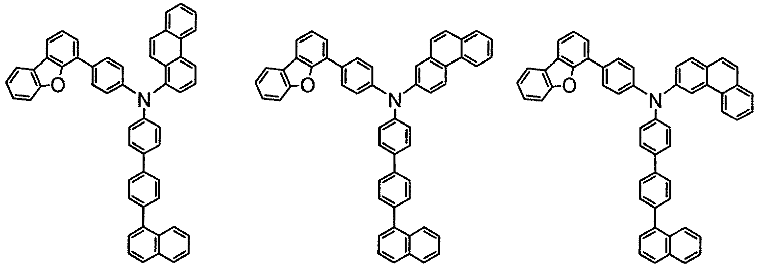
- In an embodiment of the invention, the inventive compound is preferably represented by any of the following formulae:



- In an embodiment of the invention, the inventive compound is preferably represented by any of the following formulae:


- As noted above, the "hydrogen atom" referred herein includes a light hydrogen (protium), a heavy hydrogen (deuterium), and tritium. Therefore, the inventive compound may include a naturally occurring heavy hydrogen atom.
- In addition, a heavy hydrogen atom may be intentionally introduced into the inventive compound by using a deuterated compound as a part or whole of the raw materials. Thus, in an embodiment of the invention, the inventive compound comprises at least one heavy hydrogen atom. Therefore, the inventive compound may be a compound that is represented by any of formula (A) and preferred formulae thereof, wherein at one of the hydrogen atoms included in the compound is a heavy hydrogen atom.
- Namely, in formula (A), at least one hydrogen atom selected from the hydrogen atoms in the phenyl group, the biphenylyl group, the naphthyl group, or the phenanthryl group for Ar; the hydrogen atom(s) represented by any of R1 to R7; the hydrogen atom(s) represented by any of R11 to R14; the hydrogen atom(s) represented by any of R21 to R24; the hydrogen atom(s) represented by any of R31 to R34; and the hydrogen atom(s) represented by any of R41 to R48 not the single bond bonded to *1 may be a heavy hydrogen atom.
- The deuteration rate of the deuterated compound (the ratio of the number of heavy hydrogen atoms to the total number of hydrogen atoms in the inventive compound) depends on the deuteration rate of the raw material to be used. It is generally difficult to use the raw materials each having a deuteration rate of 100%. Therefore, the deuteration rate of the inventive compound is less than 100% and 1% or more, preferably 3% or more, more preferably 5% or more, and still more preferably 10% or more.
- The inventive compound may be a mixture of a deuterated compound and a non-deuterated compound or a mixture of two or more compounds having different deuteration rates. The deuteration rate of such a mixture (the ratio of the number of heavy hydrogen atoms to the total number of hydrogen atoms each in the mixture) is 1% or more, preferably 3% or more, more preferably 5% or more, and still more preferably 10% or more, and less than 100%.
- In the inventive compound, at least one hydrogen atom selected from the hydrogen atoms in the phenyl group, the biphenylyl group, the naphthyl group, or the phenanthryl group for Ar may be a heavy hydrogen atom. The deuteration rate (the ratio of the number of heavy hydrogen atoms to the total number of hydrogen atoms each in Ar) is 1% or more, preferably 3% or more, more preferably 5% or more, and still more preferably 10% or more, and less than 100%.
- In the inventive compound, at least one hydrogen atom selected from the hydrogen atom(s) represented by any of R1 to R7 may be a heavy hydrogen atom. The deuteration rate (the ratio of the number of heavy hydrogen atoms to the total number of hydrogen atoms each represented by R1 to R7) is 1% or more, preferably 3% or more, more preferably 5% or more, and still more preferably 10% or more, and less than 100%.
- In the inventive compound, at least one hydrogen atom selected from the hydrogen atom(s) represented by any of R11 to R14 may be a heavy hydrogen atom. The deuteration rate (the ratio of the number of heavy hydrogen atoms to the total number of hydrogen atoms each represented by R11 to R14) is 1% or more, preferably 3% or more, more preferably 5% or more, and still more preferably 10% or more, and less than 100%.
- In the inventive compound, at least one hydrogen atom selected from the hydrogen atom(s) represented by any of R21 to R24 may be a heavy hydrogen atom. The deuteration rate (the ratio of the number of heavy hydrogen atoms to the total number of hydrogen atoms each represented by R21 to R24) is 1% or more, preferably 3% or more, more preferably 5% or more, and still more preferably 10% or more, and less than 100%.
- In the inventive compound, at least one hydrogen atom selected from the hydrogen atom(s) represented by any of R31 to R34 may be a heavy hydrogen atom. The deuteration rate (the ratio of the number of heavy hydrogen atoms to the total number of hydrogen atoms each represented by R31 to R34) is 1% or more, preferably 3% or more, more preferably 5% or more, and still more preferably 10% or more, and less than 100%.
- In the inventive compound, at least one hydrogen atom selected from the hydrogen atom(s) represented by any of R41 to R48 not the single bond bonded to *1 may be a heavy hydrogen atom. The deuteration rate (the ratio of the number of heavy hydrogen atoms to the total number of hydrogen atoms each represented by R41 to R48 not the single bond bonded to *1) is 1% or more, preferably 3% or more, more preferably 5% or more, and still more preferably 10% or more, and less than 100%.
- One of ordinary skill in the art could easily produce the inventive compound by referring to the Synthesis Examples mentioned below and known synthesis methods.
- Examples of the inventive compound are shown below, although not limited thereto. D in the following examples means a heavy hydrogen atom.


- The material for organic electroluminescence devices comprises the inventive compound. The content of the inventive compound in the material for organic electroluminescence devices is, for example, 1% by mass or more (inclusive of 100%), preferably 10% by mass or more (inclusive of 100%), more preferably 50% by mass or more (inclusive of 100%), still more preferably 80% by mass or more (inclusive of 100%), and particularly preferably 90% by mass or more (inclusive of 100%). The material for organic electroluminescence devices is useful for the production of an organic EL device.
- The organic electroluminescence device of the invention comprises an anode, a cathode, and an organic layer disposed between the anode and the cathode. The organic layer comprises a light emitting layer and at least one layer of the organic layer comprises the inventive compound.
- Examples of the organic layer which comprises the inventive compound include a hole transporting region formed between an anode and a light emitting layer, such as a hole transporting layer, a hole injecting layer, an electron blocking layer, and an exciton blocking layer, a light emitting layer, a space layer, and an electron transporting region formed between a cathode and a light emitting layer, such as an electron transporting layer, an electron injecting layer, and a hole blocking layer, although not limited thereto. The inventive compound is used for the production of a fluorescent or phosphorescent EL device preferably as a material for a hole transporting region or a light emitting layer, more preferably as a material for a hole transporting region, still more preferably as a material for a hole transporting layer, an electron blocking layer or an exciton blocking layer, and particularly preferably an electron blocking layer or an exciton blocking layer.
- The organic EL device of the invention may be any of a fluorescent or phosphorescent single color emitting device, a white-emitting device of fluorescent-phosphorescent hybrid type, a simple-type emitting device having a single emission unit, and a tandem emitting device having two or more emission units, with a fluorescent device being preferred. The "emission unit" referred to herein is the smallest unit for emitting light by the recombination of injected holes and injected electrons, which comprises an organic layer, wherein at least one layer is a light emitting layer.
- Representative device structures of the simple-type organic EL device are shown below:
- The emission unit may be a multi-layered structure comprising two or more layers selected from a phosphorescent light emitting layer and a fluorescent light emitting layer. A space layer may be disposed between the light emitting layers to prevent the diffusion of excitons generated in the phosphorescent light emitting layer into the fluorescent light emitting layer. Representative layered structures of the simple-type emission unit are shown below, wherein the layers in parentheses are optional:
- (a) (Hole injecting layer/)Hole transporting layer/Fluorescent emitting layer/Electron transporting layer(/Electron injecting layer);
- (b) (Hole injecting layer/)Hole transporting layer/Phosphorescent emitting layer/Electron transporting layer(/Electron injecting layer);
- (c) (Hole injecting layer/)Hole transporting layer/First fluorescent emitting layer/Second fluorescent emitting layer/Electron transporting layer(/Electron injecting layer);
- (d) (Hole injecting layer/)Hole transporting layer/First phosphorescent emitting layer/Second phosphorescent emitting layer/Electron transporting layer(/Electron injecting layer);
- (e) (Hole injecting layer/)Hole transporting layer/Phosphorescent emitting layer/Space layer/Fluorescent emitting layer/Electron transporting layer(/Electron injecting layer);
- (f) (Hole injecting layer/)Hole transporting layer/First phosphorescent emitting layer/Second phosphorescent emitting layer/Space layer/Fluorescent emitting layer/Electron transporting layer(/Electron injecting layer);
- (g) (Hole injecting layer/)Hole transporting layer/First phosphorescent emitting layer/Space layer/Second phosphorescent emitting layer/Space layer/Fluorescent emitting layer/Electron transporting layer(/Electron injecting layer);
- (h) (Hole injecting layer/)Hole transporting layer/Phosphorescent emitting layer/Space layer/First fluorescent emitting layer/Second fluorescent emitting layer/Electron transporting layer(/Electron injecting layer);
- (i) (Hole injecting layer/)Hole transporting layer/Electron blocking layer/Fluorescent emitting layer/Electron transporting layer(/Electron injecting layer);
- (j) (Hole injecting layer/)Hole transporting layer/Electron blocking layer/Phosphorescent emitting layer/Electron transporting layer(/Electron injecting layer);
- (k) (Hole injecting layer/)Hole transporting layer/Exciton blocking layer/Fluorescent emitting layer/Electron transporting layer(/Electron injecting layer);
- (l) (Hole injecting layer/)Hole transporting layer/Exciton blocking layer/Phosphorescent emitting layer/Electron transporting layer(/Electron injecting layer);
- (m) (Hole injecting layer/)First hole transporting layer/Second hole transporting layer/Fluorescent emitting layer/Electron transporting layer(/Electron injecting layer);
- (n) (Hole injecting layer/)First hole transporting layer/Second hole transporting layer/Phosphorescent emitting layer/Electron transporting layer(/Electron injecting layer);
- (o) (Hole injecting layer/)First hole transporting layer/Second hole transporting layer/Fluorescent emitting layer/First electron transporting layer/Second electron transporting layer(/Electron injecting layer);
- (p) (Hole injecting layer/)First hole transporting layer/Second hole transporting layer/Phosphorescent emitting layer/First electron transporting layer/Second electron transporting layer(/Electron injecting layer);
- (q) (Hole injecting layer/)Hole transporting layer/Fluorescent emitting layer/Hole blocking layer/Electron transporting layer(/Electron injecting layer/Electron injecting layer);
- (r) (Hole injecting layer/)Hole transporting layer/Phosphorescent emitting layer/Hole blocking layer/Electron transporting layer(/Electron injecting layer);
- (s) (Hole injecting layer/)Hole transporting layer/Fluorescent emitting layer/Exciton blocking layer/Electron transporting layer(/Electron injecting layer); and
- (t) (Hole injecting layer/)Hole transporting layer/Phosphorescent emitting layer/ Exciton blocking layer/Electron transporting layer(/Electron injecting layer).
- The emission colors of phosphorescent emitting layers or fluorescent emitting layers may be different. For example, the emission unit (f) may be (Hole injecting layer)/Hole transporting layer/First phosphorescent emitting layer (red emission)/Second phosphorescent emitting layer (green emission)/Space layer/Fluorescent emitting layer (blue emission)/Electron transporting layer.
- An electron blocking layer may be disposed between each light emitting layer and the hole transporting layer or between each light emitting layer and the space layer, if necessary. Also, a hole blocking layer may be disposed between each light emitting layer and the electron transporting layer, if necessary. With such an electron blocking layer or a hole blocking layer, electrons and holes are confined in the light emitting layer to increase the charge recombination in the light emitting layer, thereby improving the emission efficiency.
- Representative device structure of the tandem-type organic EL device is shown below:
- The layered structure of the first emission unit and the second emission unit may be selected from those described above with respect to the emission unit.
- Generally, the intermediate layer is also called an intermediate electrode, an intermediate conductive layer, a charge generation layer, an electron withdrawing layer, a connecting layer, or an intermediate insulating layer. The intermediate layer supplies electrons to the first emission unit and holes to the second emission unit and may be formed by known materials.
-
Fig. 1 is a schematic illustration showing the structure of an example of the organic EL device of the invention, wherein theorganic EL device 1 comprises asubstrate 2, ananode 3, acathode 4, and anemission unit 10 disposed between theanode 3 and thecathode 4. Theemission unit 10 comprises alight emitting layer 5. A hole transporting region 6 (for example, a hole injecting layer or a hole transporting layer) is disposed between the light emittinglayer 5 and theanode 3, and an electron transporting region 7 (for example, an electron injecting layer or an electron transporting layer) is disposed between the light emittinglayer 5 and thecathode 4. An electron blocking layer (not shown) may be disposed on theanode 3 side of thelight emitting layer 5, and a hole blocking layer (not shown) may be disposed on thecathode 4 side of thelight emitting layer 5. With these blocking layers, electrons and holes are confined in thelight emitting layer 5 to increase the exciton generation in thelight emitting layer 5. -
Fig. 2 is a schematic illustration showing the structure of another example of the organic EL device, wherein theorganic EL device 11 comprises asubstrate 2, ananode 3, acathode 4, and anemission unit 20 disposed between theanode 3 and thecathode 4. Theemission unit 20 comprises alight emitting layer 4. The hole transporting region disposed between theanode 3 and thelight emitting layer 5 is formed by a firsthole transporting layer 6a and a secondhole transporting layer 6b. The electron transporting region disposed between the light emittinglayer 5 and thecathode 4 is formed by a firstelectron transporting layer 7a and a secondelectron transporting layer 7b. - In the present invention, a host is referred to as a fluorescent host when combinedly used with a fluorescent dopant (fluorescent emitting material) and as a phosphorescent host when combinedly used with a phosphorescent dopant (phosphorescent emitting material). Therefore, the fluorescent host and the phosphorescent host are not distinguished from each other merely by the difference in their molecular structures. Namely, in the present invention, the term "phosphorescent host" means a material for constituting a phosphorescent emitting layer containing a phosphorescent dopant and does not mean a material that cannot be used as a material for a fluorescent emitting layer. The same applies to the fluorescent host.
- The substrate is a support for the emitting device and made of, for example, glass, quartz, and plastics. The substrate may be a flexible substrate, for example, a plastic substrate made of polycarbonate, polyarylate, polyether sulfone, polypropylene, polyester, polyvinyl fluoride, or polyvinyl chloride. An inorganic deposition film is also usable.
- The anode is formed on the substrate preferably from a metal, an alloy, an electrically conductive compound, and a mixture thereof, each having a large work function, for example, 4.0 eV or more. Examples of the material for the anode include indium oxide-tin oxide (ITO: indium tin oxide), indium oxide-tin oxide doped with silicon or silicon oxide, indium oxide-zinc oxide, indium oxide doped with tungsten oxide and zinc oxide, and graphene. In addition, gold (Au), platinum (Pt), nickel (Ni), tungsten (W), chromium (Cr), molybdenum (Mo, iron (Fe), cobalt (Co), copper (Cu), palladium (Pd), titanium (Ti), and a nitride of the above metal (for example, titanium nitride) are also usable.
- These anode materials are made into a film generally by a sputtering method. For example, a film of indium oxide-zinc oxide is formed by sputtering an indium oxide target doped with 1 to 10 wt% of zinc oxide, and a film of indium oxide doped with tungsten oxide and zinc oxide is formed by sputtering an indium oxide target doped with 0.5 to 5 wt% of tungsten oxide and 0.1 to 1 wt% of zinc oxide. In addition, a vacuum vapor deposition method, a coating method, an inkjet method, and a spin coating method are usable.
- A hole injecting layer to be optionally formed in contact with the anode is formed from a material which is capable of easily injecting holes independently of the work function of the anode. Therefore, the anode can be formed by a material generally known as an electrode material, for example, a metal, an alloy, an electroconductive compound, a mixture thereof, and a
group 1 element and agroup 2 element of the periodic table. - A material having a small work function belonging to a
group 1 or agroup 2 of the periodic table, for example, an alkali metal, such as lithium (Li) and cesium (Cs), an alkaline earth metal, such as magnesium (Mg), calcium (Ca), and strontium (Sr), and an alloy thereof, such as MgAg and AlLi, are also usable as an anode material. In addition, a rare earth metal, such as europium and ytterbium, and an alloy thereof are also usable. The alkali metal, the alkaline earth metal, and the alloy thereof is made into the anode by a vacuum vapor deposition or a sputtering method. When a silver paste is used, a coating method and an inkjet method are usable. - The hole injecting layer comprises a material having a high hole injecting ability (hole injecting material) and formed between an anode and a light emitting layer or between an anode and a hole transporting layer, if present.
- Examples of the hole injecting material include molybdenum oxide, titanium oxide, vanadium oxide, rhenium oxide, ruthenium oxide, chromium oxide, zirconium oxide, hafnium oxide, tantalum oxide, silver oxide, tungsten oxide, and manganese oxide.
- The following low molecular aromatic amine compound is also usable as the hole injecting layer material: 4,4',4"-tris(N,N-diphenylamino)triphenylamine (TDATA), 4,4',4"-tris[N-(3-methylphenyl)-N-phenylamino]triphenylamine (MTDATA), 4,4'-bis[N-(4-diphenylaminophenyl)-N-phenylamino]biphenyl (DPAB), 4,4'-bis(N-{4-[N'-(3-methylphenyl)-N'-phenylamino]phenyl}-N-phenylamino)biphenyl (DNTPD), 1,3,5-tris[N-(4-diphenylaminophenyl)-N-phenylamino]benzene (DPA3B), 3-[N-(9-phenylcarbazole-3-yl)-N-phenylamino]-9-phenylcarbazole (PCzPCA1), 3,6-bis[N-(9-phenylcarbazole-3-yl)-N-phenylamino]-9-phenylcarbazole (PCzPCA2), and 3-[N-(1-naphthyl)-N-(9-phenylcarbazole-3-yl)amino]-9-phenylcarbazole (PCzPCN1).
- A macromolecular compound, such as an oligomer, a dendrimer, a polymer, is also usable as the hole injecting layer material. Examples thereof include poly(N-vinylcarbazole) (PVK), poly(4-vinyltriphenylamine) (PVTPA), poly[N-(4-{N'-[4-(4-diphenylamino)phenyl]phenyl-N'-phenylamino}phenyl)methacrylamide] (PTPDMA), and poly[N,N'-bis(4-butylphenyl)-N,N'-bis(phenyl)benzidine] (Poly-TPD). A macromolecular compound doped with an acid, such as poly(3,4-ethylenedioxythiophene)/poly(styrenesulfonic acid) (PEDOT/PSS) and polyaniline/poly(styrenesulfonic acid) (PAni/PSS), is also usable.
- In addition, an acceptor material, such as a hexaazatriphenylene (HAT) compound represented by formula (K), is preferably used:

- R21 to R26 are each independently a cyano group, -CONH2, a carboxyl group, or -COOR27 wherein R27 is an alkyl group having 1 to 20 carbon atoms or a cycloalkyl group having 3 to 20 ring carbon atoms, or
- adjacent two selected from R21 and R22, R23 and R24, and R25 and R26 may be bonded to each other to form a group represented by -CO-O-CO-.
- Examples of R27 include a methyl group, an ethyl group, a n-propyl group, an isopropyl group, a n-butyl group, an isobutyl group, a t-butyl group, a cyclopentyl group, and a cyclohexyl group.
- The hole transporting layer comprises a material having a high hole transporting ability (hole transporting material) and formed between an anode and a light emitting layer or between a hole injecting layer, if present, and a light emitting layer. The inventive compound is preferably used in a hole transporting layer alone or in combination with the compound described below.
- The hole transporting layer may be a single layer or a multi-layer of two or more layers. For example, the hole transporting layer may be a two-layered structure comprising a first hole transporting layer (anode side) and a second hole transporting layer (cathode side). In an embodiment of the invention, a hole transporting layer of a single-layered structure is preferably in contact with a light emitting layer and a hole transporting layer in a multi-layered structure which is closest to a cathode, for example, the second hole transporting layer in the two-layered structure mentioned above, is preferably in contact with a light emitting layer. In another embodiment of the invention, an electron blocking layer may be disposed between the light emitting layer and the hole transporting layer of the single-layered structure or between the light emitting layer and the hole transporting layer in the multi-layered structure which is closest to the light emitting layer.
- In the two-layered structure of the hole transporting layer, the inventive compound may be included in one or both of the first hole transporting layer and the second hole transporting layer. In an embodiment of the invention, the inventive compound is preferably used in the first hole transporting layer. In another embodiment, the inventive compound is preferably used in the second hole transporting layer. In still another embodiment, the inventive compound is preferably used in both the first hole transporting layer and the second hole transporting layer.
- In an embodiment of the invention, the inventive compound used in one or both of the first hole transporting layer and the second hole transporting layer is preferably a light-hydrogen analogue in view of production cost.
- The light-hydrogen analogue means the inventive compound wherein all the hydrogen atoms are light hydrogen atoms.
- Thus, the present invention includes an organic EL device comprising the inventive compound in one or both of the first hole transporting layer and the second hole transporting layer, wherein the inventive compound is substantially a light-hydrogen analogue. The words "the inventive compound is substantially a light-hydrogen analogue" used herein means that the content of the light-hydrogen analogue in the total amount of the inventive compound is 90 mol % or more, preferably 95 mol % or more, and still more preferably 99 mol % or, each inclusive of 100%.
- Examples of the hole transporting material other than the inventive compound includes an aromatic amine compound, a carbazole derivative, and an anthracene derivative.
- Examples of the aromatic amine compound include 4,4'-bis[N-(1-naphthyl)-N-phenylamino]biphenyl (NPB), N,N'-bis(3-methylphenyl)-N,N'-diphenyl-[1,1'-biphenyl]-4,4'-diamine (TPD), 4-phenyl-4'-(9-phenylfluorene-9-yl)triphenylamine (BAFLP), 4,4'-bis[N-(9,9-dimethylfluorene-2-yl)-N-phenylamino]biphenyl (DFLDPBi), 4,4',4"-tris(N,N-diphenylamino)triphenylamine (TDATA), 4,4',4"-tris[N-(3-methylphenyl)-N-phenylamino]triphenylamine (MTDATA), and 4,4'-bis[N-(spiro-9,9'-bifluorene-2-yl)-N-phenylamino]biphenyl (BSPB). The above compounds have a hole mobility of 10-6 cm2/Vs or more.
- Examples of the carbazole derivative include 4,4'-di(9-carbazolyl)biphenyl (CBP), 9-[4-(9-carbazolyl)phenyl]-10-phenylanthracene (CzPA), and 9-phenyl-3-[4-(10-phenyl-9-anthryl)phenyl]-9H-carbazole (PCzPA).
- Examples of the anthracene derivative include 2-t-butyl-9,10-di(2-naphthyl)anthracene (t-BuDNA), 9,10-di(2-naphthyl)anthracene (DNA), and 9,10-diphenylanthracene (DPAnth).
- In addition, a macromolecular compound, such as poly(N-vinylcarbazole) (PVK) and poly(4-vinyltriphenylamine) (PVTPA) are usable.
- Compounds other than those mentioned above are also usable, if their hole transporting ability is higher than their electron transporting ability.
- The light emitting layer comprises a highly light-emitting material (dopant material) and may be formed from a various kind of materials. For example, a fluorescent emitting material and a phosphorescent emitting material are usable as the dopant material. The fluorescent emitting material is a compound capable of emitting light from a singlet excited state, and the phosphorescent emitting material is a compound capable of emitting light from a triplet excited state.
- Examples of blue fluorescent emitting material usable in the light emitting layer include a pyrene derivative, a styrylamine derivative, a chrysene derivative, a fluoranthene derivative, a fluorene derivative, a diamine derivative, and a triarylamine derivative, such as N,N'-bis[4-(9H-carbazole-9-yl)phenyl]-N,N'-diphenylstilbene-4,4'-diamine (YGA2S), 4-(9H-carbazole-9-yl)-4'-(10-phenyl-9-anthryl)triphenylamine (YGAPA), and 4-(10-phenyl-9-anthryl)-4'-(9-phenyl-9H-carbazole-3-yl)triphenylamine (PCBAPA).
- Examples of green fluorescent emitting material usable in the light emitting layer include an aromatic amine derivative, such as N-(9,10-diphenyl-2-anthryl)-N,9-diphenyl-9H-carbazole-3-amine (2PCAPA), N-[9,10-bis(1,1'-biphenyl-2-yl)-2-anthryl]-N,9-diphenyl-9H-carbazole-3-amine (2PCABPhA), N-(9,10-diphenyl-2-anthryl)-N,N',N'-triphenyl-1,4-phenylenediamine (2DPAPA), N-[9,10-bis(1,1'-biphenyl-2-yl)-2-anthryl]-N,N',N'-triphenyl-1,4-phenylenediamine (2DPABPhA), N-[9,10-bis(1,1'-biphenyl-2-yl)]-N-[4-(9H-carbazole-9-yl)phenyl]-N-phenylanthracene-2-amine (2YGABPhA), and N,N,9-triphenylanthracene-9-amine (DPhAPhA).
- Examples of red fluorescent emitting material usable in the light emitting layer include a tetracene derivative and a diamine derivative, such as N,N,N',N'-tetrakis(4-methylphenyl)tetracene-5,11-diamine (p-mPhTD) and 7,14-diphenyl-N,N,N',N'-tetrakis(4-methylphenyl)acenaphtho[1,2-a]fluoranthene-3,10-diamine (p-mPhAFD).
- Examples of blue phosphorescent emitting material usable in the light emitting layer include a metal complex, such as an iridium complex, an osmium complex, and a platinum complex. Examples thereof include bis[2-(4',6'-difluorophenyl)pyridinato-N,C2']iridium(III) tetrakis(1-pyrazolyl)borato (FIr6), bis[2-(4',6'-difluorophenyl)pyridinato-N,C2']iridium(III) picolinato (FIrpic), bis[2-(3',5'-bistrifluoromethylphenyl)pyridinato-N,C2']iridium(III) picolinato (Ir(CF3ppy)2(pic)), and bis[2-(4',6'-difluorophenyl)pyridinato-N,C2']iridium(III) acetylacetonato (FIracac).
- Examples of green phosphorescent emitting material usable in the light emitting layer include an iridium complex, such as tris(2-phenylpyridinato-N,C2')iridium(III) (Ir(ppy)3), bis(2-phenylpyridinato-N,C2')iridium(III) acetylacetonato (Ir(ppy)2(acac)), bis(1,2-diphenyl-1H-benzimidazolato)iridium(III) acetylacetonato (Ir(pbi)2(acac)), and bis(benzo[h]quinolinato)iridium(III) acetylacetonato (Ir(bzq)2(acac)).
- Examples of red phosphorescent emitting material usable in the light emitting layer include a metal complex, such as an iridium complex, a platinum complex, a terbium complex, and a europium complex. Examples thereof include an organometallic complex, such as bis[2-(2'-benzo[4,5-α]thienyl)pyridinato-N,C3']iridium(III) acetylacetonato (Ir(btp)2(acac)), bis(1-phenylisoquinolinato-N,C2')iridium(III) acetylacetonato (Ir(piq)2(acac)), (acetylacetonato)bis[2,3-bis(4-fluorophenyl)quinoxalinato]iridium(III) (Ir(Fdpq)2(acac)), and 2,3,7,8,12,13,17,18-octaethyl-21H,23H-porphyrin platinum(II) (PtOEP).
- A rare earth metal complex, such as tris(acetylacetonato) (monophenanthroline)terbium(III) (Tb(acac)3(Phen)), tris(1,3-diphenyl-1,3-propanedionato)(monophenanthroline)europium(III) (Eu(DBM)3(Phen)), and tris[1-(2-thenoyl)-3,3,3-trifluoroacetonato](monophenanthroline)europium(III) (Eu(TTA)3(Phen)), emits light from the rare earth metal ion (electron transition between different multiple states), and therefore, usable as a phosphorescent emitting material.
- The light emitting layer may be a layer wherein the above dopant material is dispersed in another material (host material). The host material preferably has a lowest unoccupied molecular orbital level (LUMO level) higher than that of the dopant material and a highest occupied molecular orbital level (HOMO level) lower than that of the dopant material.
- The host material other the compound (1) may include, for example,
- (1) a metal complex, such as an aluminum complex, a beryllium complex, and a zinc complex;
- (2) a heterocyclic compound, such as an oxadiazole derivative, a benzimidazole derivative, and a phenanthroline derivative;
- (3) a fused aromatic compound, such as a carbazole derivative, an anthracene derivative, a phenanthrene derivative, a pyrene derivative, and a chrysene derivative; and
- (4) an aromatic amine compound, such as a triarylamine derivative and a fused aromatic polycyclic amine derivative.
- Examples thereof include:
- a metal complex, such as tris(8-quinolinolato)aluminum(III) (Alq), tris(4-methyl-8-quinolinolato)aluminum(III) (Almq3), bis(10-hydroxybenzo[h]quinolinato)beryllium(II) (BeBq2), bis(2-methyl-8-quinolinolato)(4-phenylphenolato)aluminum(III) (BAlq), bis(8-quinolinolato)zinc(II) (Znq), bis[2-(2-benzoxazolyl)phenolato]zinc(II) (ZnPBO), and bis[2-(2-benzothiazolyl)phenolato]zinc(II) (ZnBTZ);
- a heterocyclic compound, such as 2-(4-biphenylyl)-5-(4-tert-butylphenyl)-1,3,4-oxadiazole (PBD), 1,3-bis[5-(p-tert-butylphenyl)-1,3,4-oxadiazole-2-yl]benzene (OXD-7), 3-(4-biphenylyl)-4-phenyl-5-(4-tert-butylphenyl)-1,2,4-triazole (TAZ), 2,2',2"-(1,3,5-benzenetriyl)tris(1-phenyMH-benzimidazole) (TPBI), bathophenanthroline (BPhen), and bathocuproin (BCP);
- a fused aromatic compound, such as 9-[4-(10-phenyl-9-anthryl)phenyl]-9H-carbazole (CzPA), 3,6-diphenyl-9-[4-(10-phenyl-9-anthryl)phenyl]-9H-carbazole (DPCzPA), 9,10-bis(3,5-diphenylphenyl)anthracene (DPPA), 9,10-di(2-naphthyl)anthracene (DNA), 2-tert-butyl-9,10-di(2-naphthyl)anthracene (t-BuDNA), 9,9'-bianthryl (BANT), 9,9'-(stilbene-3,3'-diyl)diphenanthrene (DPNS), 9,9'-(stilbene-4,4'-diyl)diphenanthrene (DPNS2), 3,3',3"-(benzene-1,3,5-triyl)tripyrene (TPB3), 9,10-diphenylanthracene (DPAnth), and 6,12-dimethoxy-5,11-diphenylchrysene; and
- an aromatic amine compound, such as N,N-diphenyl-9-[4-(10-phenyl-9-anthryl)phenyl]-9H-carbazole-3-amine (CzA1PA), 4-(10-phenyl-9-anthryl)triphenylamine (DPhPA), N,9-diphenyl-N-[4-(10-phenyl-9-anthryl)phenyl]-9H-carbazole-3-amine (PCAPA), N,9-diphenyl-N-{4-[4-(10-phenyl-9-anthryl)phenyl]phenyl}-9H-carbazole-3-amine (PCAPBA), N-(9,10-diphenyl-2-anthryl)-N,9-diphenyl-9H-carbazole-3-amine (2PCAPA), 4,4'-bis[N-(1-anthryl)-N-phenylamino]biphenyl (NPB or α-NPD), N,N'-bis(3-methylphenyl)-N,N'-diphenyl-[1,1'-biphenyl]-4,4'-diamine (TPD), 4,4'-bis[N-(9,9-dimethylfluorene-2-yl)-N-phenylamino]biphenyl (DFLDPBi), and 4,4'-bis[N-(spiro-9,9'-bifluorene-2-yl)-N-phenylamino]biphenyl (BSPB).
- The host material may be used alone or in combination of two or more.
- In particular, as a host material for a blue fluorescent device, the following anthracene compound is preferably used.


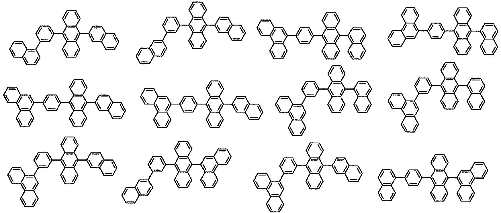


- The electron transporting layer comprises a material having a high electron transporting ability (electron transporting material) and formed between a light emitting layer and a cathode or between a light emitting layer and an electron injecting layer, if present.
- The electron transporting layer may be a single layer or a multi-layer of two or more layers. For example, the electron transporting layer may be a two-layered structure comprising a first electron transporting layer (anode side) and a second electron transporting layer (cathode side). In an embodiment of the invention, an electron transporting layer of a single-layered structure is preferably in contact with a light emitting layer and an electron transporting layer in a multi-layered structure which is closest to an anode, for example, the first electron transporting layer in the two-layered structure mentioned above, is preferably in contact with a light emitting layer. In another embodiment of the invention, an hole blocking layer mentioned below may be disposed between the light emitting layer and the electron transporting layer of the single-layered structure or between the light emitting layer and the electron transporting layer in the multi-layered structure which is closest to the light emitting layer.
- The electron transporting layer may be formed, for example, by
- (1) a metal complex, such as an aluminum complex, a beryllium complex, and a zinc complex;
- (2) a heteroaromatic compound, such as an imidazole derivative, a benzimidazole derivative, an azine derivative, a carbazole derivative, and a phenanthroline derivative; and
- (3) a macromolecular compound.
- Examples of the metal complex include tris(8-quinolinolato)aluminum (III) (Alq), tris(4-methyl-8-quinolinolato)aluminum (Almq3), bis(10-hydroxybenzo[h]quinolinato)beryllium (BeBq2), bis(2-methyl-8-quinolinato)(4-phenylphenolato)aluminum (III) (BAlq), bis(8-quinolinato)zinc(II) (Znq), bis[2-(2-benzoxazolyl)phenolato]zinc(II) (ZnPBO), and bis[2-(2-benzothiazolyl)phenolato]zinc(II) (ZnBTZ).
- Examples of the heteroaromatic compound include 2-(4-biphenylyl)-5-(4-tert-butylphenyl)-1,3,4-oxadiazole (PBD), 1,3-bis[5-(p-tert-butylphenyl)-1,3,4-oxadiazole-2-yl]benzene (OXD-7), 3-(4-tert-butylphenyl)-4-phenyl-5-(4-biphenylyl)-1,2,4-triazole (TAZ), 3-(4-tert-butylphenyl)-4-(4-ethylphenyl)-5-(4-biphenylyl)-1,2,4-triazole (p-EtTAZ), bathophenanthroline (BPhen), bathocuproine (BCP), and 4,4'-bis(5-methylbenzoxazole-2-yl)stilbene (BzOs).
- Examples of the macromolecular compound include poly[(9,9-dihexylfluorene-2,7-diyl)-co-(pyridine-3,5-diyl)] (PF-Py), and poly[(9,9-dioctylfluorene-2,7-diyl)-co-(2,2'-bipyridine-6,6'-diyl)] (PF-BPy).
- The above compounds have an electron mobility of 10-6 cm2/Vs or more. Materials other than those mentioned above are also usable in the electron transporting layer if their electron transporting ability is higher than their hole transporting ability.
- The electron injecting layer is a layer comprising a material having a high electron injecting ability, for example, an alkali metal, such as lithium (Li), cesium (Cs), an alkaline earth metal, such as magnesium (Mg), calcium (Ca), and strontium (Sr), a rare earth metal, such as europium (Eu) and ytterbium (Yb), and a compound of these metals, such as an alkali metal oxide, an alkali metal halide, an alkali metal-containing organic complex, an alkaline earth metal oxide, an alkaline earth metal halide, an alkaline earth metal-containing organic complex, a rare earth metal oxide, a rare earth metal halide, and a rare metal-containing organic complex. These compounds may be used in combination of two or more.
- In addition, an electron transporting material which is doped with an alkali metal, an alkaline earth metal or a compound thereof, for example, Alq doped with magnesium (Mg), is also usable. By using such a material, electrons are efficiently injected from the cathode.
- A composite material comprising an organic compound and an electron donor is also usable in the electron injecting layer. Such a composite material is excellent in the electron injecting ability and the electron transporting ability, because the organic compound receives electrons from the electron donor. The organic compound is preferably a compound excellent in transporting the received electrons. Examples thereof include the materials for the electron transporting layer mentioned above, such as the metal complex and the aromatic heterocyclic compound. Any compound capable of giving its electron to the organic compound is usable as the electron donor. Preferred examples thereof are an alkali metal, an alkaline earth metal, and a rare earth metal, such as lithium, cesium, magnesium, calcium, erbium, and ytterbium; an alkali metal oxide and an alkaline earth metal oxide, such as, lithium oxide, calcium oxide, and barium oxide; a Lewis base, such as magnesium oxide; and an organic compound, such as tetrathiafulvalene (TTF).
- The cathode is formed preferably from a metal, an alloy, an electrically conductive compound, or a mixture thereof, each having a small work function, for example, a work function of 3.8 eV or less. Examples of the material for the cathode include an element belonging to a
group 1 orgroup 2 of the periodic table, i.e., an alkali metal, such as lithium (Li) and cesium (Cs), an alkaline earth metal, such as magnesium (Mg), calcium (Ca), and strontium (Sr), an alloy containing these metals (for example, MgAg and AlLi), a rare earth metal, such as europium (Eu) and ytterbium (Yb), and an alloy containing a rare earth metal. - The alkali metal, the alkaline earth metal, and the alloy thereof is made into the cathode by a vacuum vapor deposition or a sputtering method. A coating method and an inkjet method are usable when a silver paste is used.
- When the electron injecting layer is formed, the material for the cathode is selected irrespective of whether the work function is large or small and various electroconductive materials, such as Al, Ag, ITO, graphene, and indium oxide-tin oxide doped with silicon or silicon oxide, are usable. These electroconductive materials are made into films by a sputtering method, an inkjet method, and a spin coating method.
- Since electric field is applied to the ultra-thin films of organic EL devices, the pixel defects due to leak and short circuit tends to occur. To prevent the defects, an insulating thin film layer may be interposed between the pair of electrodes.
- Examples of the material for the insulating layer include aluminum oxide, lithium fluoride, lithium oxide, cesium fluoride, cesium oxide, magnesium oxide, magnesium fluoride, calcium oxide, calcium fluoride, aluminum nitride, titanium oxide, silicon oxide, germanium oxide, silicon nitride, boron nitride, molybdenum oxide, ruthenium oxide, and vanadium oxide. These materials may be used in combination or may be used in each layer of stacked layers.
- For example, in an organic EL device having a fluorescent emitting layer and a phosphorescent emitting layer, a space layer is disposed between the fluorescent emitting layer and the phosphorescent emitting layer to prevent the diffusion of excitons generated in the phosphorescent emitting layer to the fluorescent emitting layer or to control the carrier (charge) balance. The space layer may be disposed between two or more phosphorescent emitting layers.
- Since the space layer is disposed between the light emitting layers, a material combining the electron transporting ability and the hole transporting ability is preferably used for forming the space layer. To prevent the diffusion of triplet energy in the adjacent phosphorescent emitting layer, the triplet energy of the material for the space layer is preferably 2.6 eV or more. The materials described with respect to the hole transporting layer are usable as the material for the space layer.
- A blocking layer, such as an electron blocking layer, a hole blocking layer, and an exciton blocking layer, may be provided in the portion adjacent to the light emitting layer. The electron blocking layer is a layer which prevents the diffusion of electrons from the light emitting layer to the hole transporting layer. The hole blocking layer is a layer which prevents the diffusion of holes from the light emitting layer to the electron transporting layer. The exciton blocking layer prevents the diffusion of excitons generated in the light emitting layer to adjacent layers and has a function of confining the excitons in the light emitting layer.
- Each layer of the organic EL device is formed by a known method, such as a vapor deposition method and a coating method. For example, each layer is formed by a known vapor deposition method, such as a vacuum vapor deposition method and a molecular beam evaporation method (MBE method), and a known coating method using a solution of a compound for forming a layer, such as a dipping method, a spin coating method, a casting method, a bar coating method, and a roll coating method.
- The thickness of each layer is not particularly limited and preferably 5 nm to 10 µm, more preferably 10 nm to 0.2 µm, because an excessively small thickness may cause defects such as pin holes and an excessively large thickness may require a high driving voltage.
- The organic EL device can be used in an electronic device, for example, as display parts, such as organic EL panel module, display devices of television sets, mobile phones, personal computer, etc., and light emitting sources of lighting equipment and vehicle lighting equipment.
- The present invention will be described below in more details with reference to the examples. However, it should be noted that the scope of the invention is not limited thereto.
- Compounds used in the production of organic EL devices of Examples 1 to 6:


- Comparative compounds used in the production of organic EL devices of Comparative Examples 1 to 4:


- The comparative compound Ref-1 is described in
Patent Literature 2 and the comparative compounds Ref-2, Ref-3, and Ref-4 are described inPatent Literature 1. - Other compounds used in the production of organic EL devices of Examples 1 to 6 and Comparative Examples 1 to 4:


- Each organic EL device was produced in the following manner and evaluated for EL device performance.
- A 25 mm × 75 mm × 1.1 mm glass substrate having ITO transparent electrode (anode) (product of Geomatec Company) was ultrasonically cleaned in isopropyl alcohol for 5 min and then UV/ozone cleaned for 30 min. The thickness of ITO transparent electrode was 130 nm.
- The cleaned glass substrate having a transparent electrode line was mounted to a substrate holder of a vacuum vapor deposition apparatus. First, the compound HI-1 was vapor-deposited on the surface having the transparent electrode line so as to cover the transparent electrode to form a hole injecting layer with a thickness of 5 nm.
- On the hole injecting layer, the compound HT-1 was vapor-deposited to form a first hole transporting layer with a thickness of 80 nm.
- On the first hole transporting layer, the compound Inv-1 was vapor-deposited to form a second hole transporting layer with a thickness of 10 nm.
- Then, on the second hole transporting layer, the compound BH-1 (host material) and the compound BD-1 (dopant material) were vapor co-deposited to form a light emitting layer with a thickness of 25 nm. The concentration of the compound BD-1 in the light emitting layer was 4.0% by mass.
- Then, on the light emitting layer, the compound ET-1 was vapor-deposited to form a first electron transporting layer with a thickness of 10 nm.
- On the first electron transporting layer, the compound ET-2 was vapor-deposited to form a second electron transporting layer with a thickness of 15 nm, thereby forming a second electron transporting layer.
- On the second electron transporting layer, LiF was vapor-deposited to form an electron injecting electrode (cathode) with a thickness of 1 nm.
- Then, metallic Al was vapor-deposited on the electron injecting electrode to form a metallic cathode with a thickness of 80 nm.
- The layered structure of the organic EL device of Example 1 is shown below:
ITO (130) /HI-1 (5) /HT-1 (80) /Compound Inv-1 (10) /BH-1:BD-1=96:4 (25) /ET-1 (10) /ET-2 (15) /LiF (1) /Al (80) wherein the numerals in parenthesis is the thickness (nm) and the ratio of BH-1 and BD-1 is based on mass. - Each organic EL device was produced in the same manner as in Example 1 except for using each compound described in Table 1 as the second hole transporting layer material in place of the compound Inv-1.
- Each organic EL device was produced in the same manner as in Example 1 except for using each compound described in Table 1 as the second hole transporting layer material in place of compound Inv-1.
- Each of the organic EL devices produced above was measured for external quantum efficiency. The results are shown in Table 1.
- The organic EL device thus produced was operated by a constant direct current at room temperature at a current density of 10 mA/cm2 to measure the luminance by a luminance meter (spectroradiometer CS-1000 manufactured by Minolta). The external quantum efficiency (%) was determined by the results.
Table 1 Second hole transporting layer material External quantum efficiency (%) @10mA/cm2 Example 1 Compound Inv-1 9.6 Example 2 Compound Inv-2 9.9 Example 3 Compound Inv-3 10.0 Example 4 Compound Inv-4 9.9 Example 5 Compound Inv-5 9.6 Example 6 Compound Inv-12 9.9 Comparative Example 1 Compound Ref-1 8.7 Comparative Example 2 Compound Ref-2 9.2 Comparative Example 3 Compound Ref- 3 9.1 Comparative Example 4 Compound Ref-4 8.6 - As seen from the results of Table 1, the organic EL device comprising any of the compounds Inv-1 to Inv-5 and Inv-12 of formula (1) of the invention showed a high efficiency (high external quantum efficiency).
- In contrast, the organic EL device comprising any of the compound Ref-1 described in
Patent Literature 2 and any of the compounds Ref-2, Ref-3, and Ref-4 each described inPatent Literature 1 showed a poor efficiency (external quantum efficiency). - Upon comparing Examples 1 and 5 with Comparative Examples 1, 2, and 4, it can be found that a high efficiency is obtained when a 1-naphthyl group is bonded to the central nitrogen group via a p-biphenylylene linker.
- Upon comparing Examples 1 to 6 with Comparative Example 3, it can be found that a high efficiency is obtained when Ar defined in formula (1) is present on the central nitrogen atom.
- Compounds synthesized in Synthesis Examples
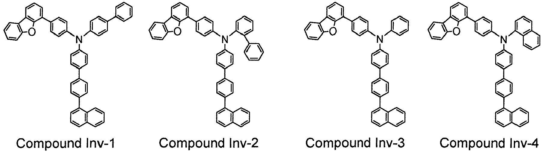


-

- In an argon atmosphere, Amine 1 (20 mmol, 5.2 g), Chloride 1 (20 mmol, 6.3 g), tris(dibenzylideneacetone)dipalladium(0) (0.4 mmol, 366 mg), 2, 2'-bis(diphenylphosphino)-1,1'-binaphthyl (0.4 mmol, 249 mg), sodium tert-butoxide (28 mmol, 2.7 g), and toluene (100 mL) were charged in a flask and stirred at 80 °C for 5 h under heating.
- After cooling to room temperature (25 °C), the reaction solution was concentrated and the obtained residue was purified by a silica gel column chromatography to obtain a white solid (8.28 g, yield of 77%), which was identified as the intermediate 1 by LC-MS analysis.
-

- In an argon atmosphere, the intermediate 1 (7 mmol, 3.8 g), 4-bromobiphenyl (7 mmol, 1.6 g), tris(dibenzylideneacetone)dipalladium(0) (0.14 mmol, 128 mg), tri-tert-butylphosphonium tetrafluoroborate (0.56 mmol, 162 mg), sodium tert-butoxide (9.8 mmol, 942 mg), and xylene (35 mL) were charged in a flask and refluxed for 4 h by stirring under heating.
- After cooling to room temperature (25 °C), the reaction solution was concentrated and the obtained residue was purified by a silica gel column chromatography to obtain a white solid (4.0 g, yield of 83%), which was identified as the compound Inv-1 by LC-MS analysis.
-

- In the same manner as in Synthesis Example 1 except for using 2-bromobiphenyl in place of 4-bromobiphenyl, a white powder (3.8 g, yield of 78%) was obtained, which was identified as the compound Inv-2 by LC-MS analysis.
-

- In the same manner as in Synthesis Example 1 except for using bromobenzene in place of 4-bromobiphenyl, a white powder (3.0 g, yield of 69%) was obtained, which was identified as the compound Inv-3 by LC-MS analysis.
-

- In the same manner as in Synthesis Example 1 except for using 1-iodonaphthalene in place of 4-bromobiphenyl, a white powder (2.7 g, yield of 58%) was obtained, which was identified as the compound Inv-4 by LC-MS analysis.
-

- In the same manner as in Synthesis Example 1 except for using 9-bromophenanthlene in place of 4-bromobiphenyl, a white powder (2.9 g, yield of 58%) was obtained, which was identified as the compound Inv-5 by LC-MS analysis.
-

- In the same manner as in Synthesis Example 1 except for using 3-bromobiphenyl in place of 4-bromobiphenyl, a white powder (4.1 g, yield of 85%) was obtained, which was identified as the compound Inv-6 by LC-MS analysis.
-

- In the same manner as in Synthesis Example 1 except for using 2-bromonaphthalene in place of 4-bromobiphenyl, a white powder (3.3 g, yield of 72%) was obtained, which was identified as the compound Inv-7 by LC-MS analysis.
-

- In the same manner as in Synthesis Example 1 except for using 1-bromophenanthlene in place of 4-bromobiphenyl, a white powder (2.5 g, yield of 50%) was obtained, which was identified as the compound Inv-8 by LC-MS analysis.
-

- In the same manner as in Synthesis Example 1 except for using 2-bromophenanthlene in place of 4-bromobiphenyl, a white powder (4.4 g, yield of 88%) was obtained, which was identified as the compound Inv-9 by LC-MS analysis.
-

- In the same manner as in Synthesis Example 1 except for using 3-bromophenanthlene in place of 4-bromobiphenyl, a white powder (3.5 g, yield of 71%) was obtained, which was identified as the compound Inv-10 by LC-MS analysis.
-
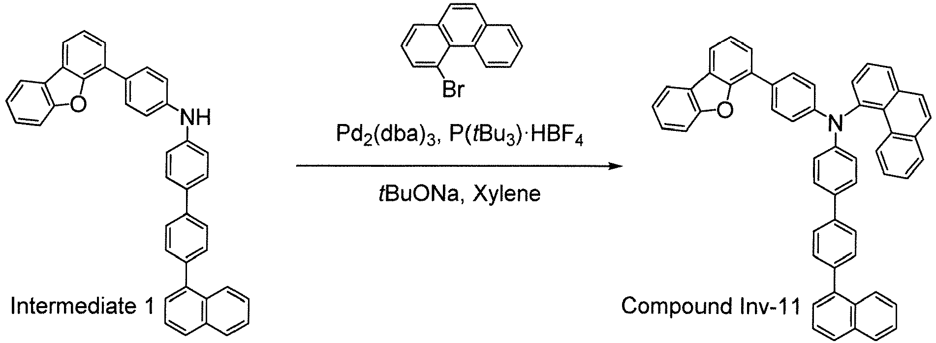
- In the same manner as in Synthesis Example 1 except for using 4-bromophenanthlene in place of 4-bromobiphenyl, a white powder (2.1 g, yield of 43%) was obtained, which was identified as the compound Inv-11 by LC-MS analysis.
-

- In the same manner as in Synthesis Example 3 except for using bromobenzene-d5 in place of bromobenzene, a white powder (3.1 g, yield of 72%) was obtained, which was identified as the compound Inv-12 by LC-MS analysis.
-
- 1, 11:
- Organic EL device
- 2:
- Substrate
- 3:
- Anode
- 4:
- Cathode
- 5:
- Light emitting layer
- 6:
- Hole transporting region (hole transporting layer)
- 6a:
- First hole transporting layer
- 6b:
- Second hole transporting layer
- 7:
- Electron transporting region (electron transporting layer)
- 7a:
- First electron transporting layer
- 7b:
- Second electron transporting layer
- 10, 20:
- Emission unit
Claims (27)
- A compound represented by formula (A):
 Ar is a substituted or unsubstituted phenyl group, a substituted or unsubstituted biphenylyl group, a substituted or unsubstituted naphthyl group, or a substituted or unsubstituted phenanthryl group;R1 to R7 are each independently a hydrogen atom, a halogen atom, an alkyl group having 1 to 10 carbon atoms, or a cycloalkyl group having 3 to 6 ring carbon atoms;R11 to R14 are each independently a hydrogen atom, a halogen atom, an alkyl group having 1 to 10 carbon atoms, or a cycloalkyl group having 3 to 6 ring carbon atoms;R21 to R24 are each independently a hydrogen atom, a halogen atom, an alkyl group having 1 to 10 carbon atoms, or a cycloalkyl group having 3 to 6 ring carbon atoms;R31 to R34 are each independently a hydrogen atom, a halogen atom, an alkyl group having 1 to 10 carbon atoms, or a cycloalkyl group having 3 to 6 ring carbon atoms;R41 to R48 are each independently a hydrogen atom, a halogen atom, an alkyl group having 1 to 10 carbon atoms, or a cycloalkyl group having 3 to 6 ring carbon atoms, provided that one selected from R47and R48 is a single bond bonded to *1;the optional substituent for the phenyl group, the biphenylyl group, the naphthyl group, and the phenanthryl group is independently a halogen atom, an alkyl group having 1 to 10 carbon atoms, or a cycloalkyl group having 3 to 6 ring carbon atoms;adjacent two selected from R1 to R7, R11 to R14, R21 to R24, R31 to R34, and R41 to R48 not the single bond bonded to *1 are not bonded to each other thereby failing to form a ring structure; andif the phenyl group, the biphenylyl group, the naphthyl group, or the phenanthryl group has adjacent two optional substituents, the adjacent two optional substituents are not bonded to each other thereby failing to form a ring.
 - The compound according to claim 1, wherein the halogen atom for the optional substituent of Ar and the halogen atom for R1 to R7, R11 to R14, R21 to R24, R31 to R34, and R41 to R48 not the single bond bonded to *1 are each independently selected from an iodine atom, a bromine atom, a chlorine atom, and a fluorine atom.
- The compound according to claim 1, wherein the alkyl group having 1 to 10 carbon atoms for the optional substituent of Ar and the alkyl group having 1 to 10 carbon atoms for R1 to R7, R11 to R14, R21 to R24, R31 to R34, and R41 to R48 not the single bond bonded to *1 are each independently selected from a methyl group, an ethyl group, a n-propyl group, a sec-propyl group, an isopropyl group, a n-butyl group, a sec-butyl group, an isobutyl group, and a t-butyl group.
- The compound according to claim 1, wherein the cycloalkyl group having 3 to 6 ring carbon atoms for the optional substituent of Ar and the cycloalkyl group having 3 to 6 ring carbon atoms for R1 to R7, R11 to R14, R21 to R24, R31 to R34, and R41 to R48 not the single bond bonded to *1 are each independently selected from a cyclopropyl group, a cyclobutyl group, a cyclopentyl group, and a cyclohexyl group.
- The compound according to any one of claims 1 to 4, wherein the compound is represented by formula (1) or (11):


- The compound according to any one of claims 1 to 5, wherein the compound is represented by formula (2) or (12):

 R1 to R7, R11 to R14, R21 to R24, R31 to R34, and R41 to R48 are as defined in formula (A); andR51 to R55 are each independently a hydrogen atom, a halogen atom, an alkyl group having 1 to 10 carbon atoms, or a cycloalkyl group having 3 to 6 ring carbon atoms.
 - The compound according to any one of claims 1 to 5, wherein the compound is represented by formula (3) or (13):

 R1 to R7, R11 to R14, R21 to R24, R31 to R34, and R41 to R48 are as defined in formula (A); andone selected from R61 to R65 is a single bond bonded to *a, and the others of R61 to R65 and R66 to R70 are each independently a hydrogen atom, a halogen atom, an alkyl group having 1 to 10 carbon atoms, or a cycloalkyl group having 3 to 6 ring carbon atoms.
 - The compound according to claim 7, wherein formula (3) is represented by any of formulae (3a) to (3c):


 R1 to R7, R11 to R14, R21 to R24, R31 to R34, and R41 to R47 are as defined in formula (A); andR61 to R65 and R66 to R70 are as defined in formula (3).
 - The compound according to claim 7, wherein formula (13) is represented by any of formulae (13a) to (13c):

 R1 to R7, R11 to R14, R21 to R24, R31 to R34, R41 to R46, and R48 are as defined in formula (A); andR61 to R65 and R66 to R70 are as defined in formula (13).
 - The compound according to any one of claims 1 to 5, wherein the compound is represented by formula (4) or (14):
 R1 to R7, R11 to R14, R21 to R24, R31 to R34, and R41 to R48 are as defined in formula (A); andone selected from R71 and R72 is a single bond bonded to *b, and the other of R71 and R72 and R73 to R78 are each independently a hydrogen atom, a halogen atom, an alkyl group having 1 to 10 carbon atoms, or a cycloalkyl group having 3 to 6 ring carbon atoms.
 - The compound according to claim 10, wherein formula (4) is represented by formula (4a) or (4b):

 R1 to R7, R11 to R14, R21 to R24, R31 to R34, and R41 to R47 are as defined in formula (A); andR71 to R7 and R73 to R78 are as defined in formula (4).
 - The compound according to claim 10, wherein formula (14) is represented by formula (14a) or (14b):

 R1 to R7, R11 to R14, R21 to R24, R31 to R34, R41 to R46, and R48 are as defined in formula (A); andR71 to R72 and R73 to R78 are as defined in formula (14).
 - The compound according to any one of claims 1 to 5, wherein the compound is represented by formula (5) or (15):

 R1 to R7, R11 to R14, R21 to R24, R31 to R34, and R41 to R48 are as defined in formula (A); andone selected from R81 to R90 is a single bond bonded to *c, and the others of R81 to R90 are each independently a hydrogen atom, a halogen atom, an alkyl group having 1 to 10 carbon atoms, or a cycloalkyl group having 3 to 6 ring carbon atoms.
 - The compound according to claim 13, wherein formula (5) is represented by any of formulae (5a) to (5e):


 R1 to R7, R11 to R14, R21 to R24, R31 to R34, and R41 to R47 are as defined in formula (A); andR81 to R90 are as defined in formula (5).
 - The compound according to claim 13, wherein formula (15) is represented by any of formulae (15a) to (15e):


 R1 to R7, R11 to R14, R21 to R24, R31 to R34, R41 to R46, and R48 are as defined in formula (A); andR81 to R90 are as defined in formula (15).
 - The compound according to any one of claims 1 to 15, wherein R1 to R7, R11 to R14, R21 to R24, R31 to R34, R41 to R48 not the single bond bonded to *1, R51 to R55, R61 to R65 not the single bond bonded to *a, R66 to R70, R71 or R72 not the single bond bonded to *b, R73 to R78, and R81 to R90 not the single bond bonded to *c are all hydrogen atoms.
- The compound according to any one of claims 1 to 16, wherein the compound is represented by any of the following formulae:


- A material for organic electroluminescence device, comprising the compound according to any one of claims 1 to 17.
- An organic electroluminescence device comprising a cathode, an anode, and an organic layer between the cathode and the anode, wherein:the organic layer comprises a light emitting layer; andat least one layer of the organic layer comprises the compound according to any one of claims 1 to 17.
- The organic electroluminescence device according to claim 19, wherein:the organic layer comprises a hole transporting region between the anode and the light emitting layer; andthe hole transporting region comprises the compound.
- The organic electroluminescence device according to claim 20, wherein:the hole transporting region comprises a first hole transporting layer on anode side and a second hole transporting layer on cathode side; andthe first hole transporting layer, the second hole transporting layer, or both thereof comprise the compound.
- The organic electroluminescence device according to claim 21, wherein the first hole transporting layer comprises the compound.
- The organic electroluminescence device according to claim 21, wherein the second hole transporting layer comprises the compound.
- The organic electroluminescence device according to any one of claims 21 to 23, wherein the second hole transporting layer is in contact with the light emitting layer.
- The organic electroluminescence device according to any one of claims 19 to 24, wherein the light emitting layer comprises a fluorescent dopant material.
- The organic electroluminescence device according to any one of claims 19 to 24, wherein the light emitting layer comprises a phosphorescent dopant material.
- An electronic device comprising the organic electroluminescence device according to any one of claims 19 to 26.
Applications Claiming Priority (2)
| Application Number | Priority Date | Filing Date | Title |
|---|---|---|---|
| JP2019049104 | 2019-03-15 | ||
| PCT/JP2020/009500 WO2020189316A1 (en) | 2019-03-15 | 2020-03-05 | Compound, material for organic electroluminescent elements, organic electroluminescent element and electronic device |
Publications (3)
| Publication Number | Publication Date |
|---|---|
| EP3939970A1 true EP3939970A1 (en) | 2022-01-19 |
| EP3939970A4 EP3939970A4 (en) | 2022-11-09 |
| EP3939970B1 EP3939970B1 (en) | 2023-12-27 |
Family
ID=72520859
Family Applications (1)
| Application Number | Title | Priority Date | Filing Date |
|---|---|---|---|
| EP20725613.2A Active EP3939970B1 (en) | 2019-03-15 | 2020-03-05 | Compound, material for organic electroluminescence devices, organic electroluminescence device, and electronic device |
Country Status (6)
| Country | Link |
|---|---|
| US (2) | US11618740B2 (en) |
| EP (1) | EP3939970B1 (en) |
| JP (1) | JP6748335B1 (en) |
| KR (1) | KR102221900B1 (en) |
| CN (1) | CN111868046B (en) |
| WO (1) | WO2020189316A1 (en) |
Families Citing this family (11)
| Publication number | Priority date | Publication date | Assignee | Title |
|---|---|---|---|---|
| KR102495414B1 (en) * | 2017-03-08 | 2023-02-02 | 이데미쓰 고산 가부시키가이샤 | Chemical compounds, materials for organic electroluminescent devices, organic electroluminescent devices, and electronic devices |
| WO2019146781A1 (en) * | 2018-01-29 | 2019-08-01 | 出光興産株式会社 | Compound and organic electroluminescent element using same |
| CN113227083A (en) | 2018-11-30 | 2021-08-06 | 出光兴产株式会社 | Compound, material for organic electroluminescent element, and electronic device |
| US12048242B2 (en) | 2019-05-31 | 2024-07-23 | Idemitsu Kosan Co., Ltd. | Compound, material for organic electroluminescent elements, organic electroluminescent element, and electronic device |
| US11575087B1 (en) | 2020-12-25 | 2023-02-07 | Idemitsu Kosan Co., Ltd. | Organic electroluminescence device, light emitting device, organic electroluminescence display device and electronic device |
| US12369490B2 (en) | 2021-01-13 | 2025-07-22 | Idemitsu Kosan Co., Ltd. | Organic electroluminescent element, organic electroluminescent display device, and electronic device |
| WO2022230967A1 (en) | 2021-04-28 | 2022-11-03 | 出光興産株式会社 | Compound, material for organic electroluminescent elements, organic electroluminescent element, and electronic device |
| JP2025014072A (en) * | 2021-10-01 | 2025-01-29 | 出光興産株式会社 | Organic electroluminescence element, organic electroluminescence display device and electronic device |
| JP2025016806A (en) * | 2021-10-15 | 2025-02-05 | 出光興産株式会社 | Organic electroluminescence element and electronic device |
| KR20240096737A (en) * | 2021-11-05 | 2024-06-26 | 이데미쓰 고산 가부시키가이샤 | Organic electroluminescent devices and electronic devices |
| KR20230127061A (en) | 2022-02-24 | 2023-08-31 | 호도가야 가가쿠 고교 가부시키가이샤 | Arylamine compound, organic electroluminescence element and electronic device |
Family Cites Families (36)
| Publication number | Priority date | Publication date | Assignee | Title |
|---|---|---|---|---|
| KR101425423B1 (en) * | 2005-05-30 | 2014-08-01 | 시바 홀딩 인크 | Electroluminescent device |
| KR101453109B1 (en) * | 2006-04-26 | 2014-10-27 | 이데미쓰 고산 가부시키가이샤 | Aromatic amine derivative, and organic electroluminescence element using the same |
| KR102301756B1 (en) * | 2008-05-16 | 2021-09-15 | 가부시키가이샤 한도오따이 에네루기 켄큐쇼 | Triarylamine derivative, light-emitting substance, light-emitting element, light-emitting device, and electronic device |
| JP5193295B2 (en) * | 2008-05-29 | 2013-05-08 | 出光興産株式会社 | Aromatic amine derivatives and organic electroluminescence devices using them |
| JP2011088887A (en) * | 2009-09-22 | 2011-05-06 | Semiconductor Energy Lab Co Ltd | Halogenated diarylamine compound and method for synthesizing the same |
| EP2891653B1 (en) * | 2012-08-30 | 2018-01-17 | Idemitsu Kosan Co., Ltd | Aromatic amine derivative, and organic electroluminescent element using same |
| JP5848480B1 (en) * | 2014-10-28 | 2016-01-27 | 三星ディスプレイ株式會社Samsung Display Co., Ltd. | Material for organic electroluminescence device and organic electroluminescence device using the same |
| JP6576631B2 (en) * | 2014-12-15 | 2019-09-18 | 三星ディスプレイ株式會社Samsung Display Co.,Ltd. | Amine compound and organic electroluminescence device |
| US9812649B2 (en) * | 2015-02-17 | 2017-11-07 | Luminescence Technology Corp. | Indenotriphenylene-based amine derivative for organic electroluminescent device |
| US9847491B2 (en) * | 2015-04-30 | 2017-12-19 | Samsung Display Co., Ltd. | Organic light-emitting device |
| KR102560940B1 (en) * | 2015-06-17 | 2023-08-01 | 삼성디스플레이 주식회사 | Mono amine derivatives and organic electroluminescent device including the same |
| JP6661289B2 (en) * | 2015-07-08 | 2020-03-11 | 三星ディスプレイ株式會社Samsung Display Co.,Ltd. | Organic electroluminescent element material and organic electroluminescent element using the same |
| EP3133666B1 (en) | 2015-08-21 | 2020-03-11 | Samsung Display Co., Ltd. | Organic light-emitting device |
| KR102675680B1 (en) * | 2015-12-15 | 2024-06-18 | 삼성디스플레이 주식회사 | Amine compound and organic light emitting device including the same |
| KR20170075118A (en) * | 2015-12-22 | 2017-07-03 | 삼성디스플레이 주식회사 | Organic light emitting device |
| KR102083707B1 (en) * | 2016-02-11 | 2020-03-02 | 주식회사 엘지화학 | Compound and organic electroluminescent device using the sane |
| JP2020093979A (en) * | 2017-03-08 | 2020-06-18 | 出光興産株式会社 | Compound, material for organic electroluminescence device, organic electroluminescence device, and electronic device |
| KR20190020514A (en) | 2017-08-21 | 2019-03-04 | 에스케이케미칼 주식회사 | Compound for organic electroluminescent device and organic electroluminescent device comprising the same |
| KR102081739B1 (en) * | 2017-11-03 | 2020-02-26 | (주)씨엠디엘 | 2,3 substituted naphthylamine derivative organic compounds and organic electroluminescent device including the same |
| WO2019146781A1 (en) * | 2018-01-29 | 2019-08-01 | 出光興産株式会社 | Compound and organic electroluminescent element using same |
| US20200111962A1 (en) | 2018-10-03 | 2020-04-09 | Idemitsu Kosan Co., Ltd. | Organic electroluminescence device and electronic apparatus provided with the same |
| WO2020075758A1 (en) | 2018-10-09 | 2020-04-16 | 出光興産株式会社 | Organic electroluminescence element and electronic device using same |
| WO2020075759A1 (en) | 2018-10-09 | 2020-04-16 | 出光興産株式会社 | Organic electroluminescence element and electronic device using same |
| WO2020075760A1 (en) | 2018-10-09 | 2020-04-16 | 出光興産株式会社 | Organic electroluminescence element and electronic device using same |
| WO2020080416A1 (en) | 2018-10-16 | 2020-04-23 | 出光興産株式会社 | Organic electroluminescence element and electronic device |
| CN112823434B (en) | 2018-10-16 | 2025-06-03 | 出光兴产株式会社 | Organic electroluminescent element and electronic device |
| JP2022037252A (en) | 2018-11-07 | 2022-03-09 | 出光興産株式会社 | Organic electroluminescent element and electronic apparatus |
| WO2020096012A1 (en) | 2018-11-07 | 2020-05-14 | 出光興産株式会社 | Organic electroluminescent element and electronic appliance including same |
| US20220069232A1 (en) | 2018-11-07 | 2022-03-03 | Idemitsu Kosan Co.,Ltd. | Organic electroluminescence device and electronic apparatus using the same |
| JP2022037253A (en) | 2018-11-07 | 2022-03-09 | 出光興産株式会社 | Compound and organic electroluminescent element employing the same |
| CN113227083A (en) | 2018-11-30 | 2021-08-06 | 出光兴产株式会社 | Compound, material for organic electroluminescent element, and electronic device |
| JP2022053547A (en) | 2018-12-03 | 2022-04-06 | 出光興産株式会社 | Compound, material for organic electroluminescent elements, organic electroluminescent element, and electronic device |
| WO2020116562A1 (en) | 2018-12-05 | 2020-06-11 | 出光興産株式会社 | Organic electroluminescence element and electronic device |
| WO2020115933A1 (en) | 2018-12-05 | 2020-06-11 | 出光興産株式会社 | Organic electroluminescent element and electronic device using same |
| WO2020116561A1 (en) | 2018-12-05 | 2020-06-11 | 出光興産株式会社 | Organic electroluminescence element and electronic apparatus |
| CN113166089A (en) * | 2018-12-20 | 2021-07-23 | 默克专利有限公司 | Material for electronic devices |
-
2020
- 2020-03-05 WO PCT/JP2020/009500 patent/WO2020189316A1/en not_active Ceased
- 2020-03-05 JP JP2020515777A patent/JP6748335B1/en active Active
- 2020-03-05 KR KR1020207014327A patent/KR102221900B1/en active Active
- 2020-03-05 CN CN202080000925.XA patent/CN111868046B/en active Active
- 2020-03-05 EP EP20725613.2A patent/EP3939970B1/en active Active
- 2020-05-01 US US16/864,185 patent/US11618740B2/en active Active
-
2023
- 2023-01-24 US US18/158,613 patent/US20230159479A1/en active Pending
Also Published As
| Publication number | Publication date |
|---|---|
| JP6748335B1 (en) | 2020-08-26 |
| EP3939970A4 (en) | 2022-11-09 |
| KR20200112805A (en) | 2020-10-05 |
| CN111868046B (en) | 2023-08-01 |
| WO2020189316A1 (en) | 2020-09-24 |
| US20230159479A1 (en) | 2023-05-25 |
| EP3939970B1 (en) | 2023-12-27 |
| US11618740B2 (en) | 2023-04-04 |
| JPWO2020189316A1 (en) | 2021-04-08 |
| KR102221900B1 (en) | 2021-03-02 |
| US20200290985A1 (en) | 2020-09-17 |
| CN111868046A (en) | 2020-10-30 |
Similar Documents
| Publication | Publication Date | Title |
|---|---|---|
| EP3939970B1 (en) | Compound, material for organic electroluminescence devices, organic electroluminescence device, and electronic device | |
| US12384739B2 (en) | Compound, material for organic electroluminescent elements, organic electroluminescent element and electronic device | |
| WO2020111253A1 (en) | Compound, material for organic electroluminescent elements, organic electroluminescent element and electronic device | |
| JPWO2017022730A1 (en) | COMPOUND, MATERIAL FOR ORGANIC ELECTROLUMINESCENT ELEMENT, ORGANIC ELECTROLUMINESCENT ELEMENT, AND ELECTRONIC DEVICE | |
| CN114514221A (en) | Compound, material for organic electroluminescent element, and electronic device | |
| EP4238956A1 (en) | Compound, material for organic electroluminescent element, organic electroluminescent element, and electronic appliance | |
| WO2021193654A1 (en) | Compound, material for organic electroluminescent elements, organic electroluminescent element, and electronic device | |
| EP3360859B1 (en) | Compound, material for organic electroluminescence elements, organic electroluminescence element, and electronic device | |
| EP3790857B1 (en) | Compound, material for organic electroluminescence element, organic electroluminescence element and electronic device | |
| WO2016204151A1 (en) | Compound, material for organic electroluminescence element, organic electroluminescence element, and electronic device | |
| JP2019199442A (en) | Compound, material for organic electroluminescent element, organic electroluminescent element, and electronic device | |
| JP7351039B2 (en) | Compounds, materials for organic electroluminescent devices, organic electroluminescent devices and electronic devices | |
| KR20240137576A (en) | Compounds, materials for organic electroluminescent devices, organic electroluminescent devices, and electronic devices | |
| EP4083025A1 (en) | Compound, material for organic electroluminescent element, organic electroluminescent element and electronic device | |
| US20220281856A1 (en) | Compound, material for organic electroluminescent element, organic electroluminescent element, and electronic device | |
| KR20250137122A (en) | Compounds, materials for organic electroluminescent devices, organic electroluminescent devices and electronic devices | |
| KR20240026282A (en) | Compounds, materials for organic electroluminescent devices, organic electroluminescent devices, and electronic devices | |
| WO2023027173A1 (en) | Compound, organic electroluminescent element material, organic electroluminescent element, and electronic device | |
| KR20250144393A (en) | Compounds, materials for organic electroluminescent devices, organic electroluminescent devices and electronic devices | |
| WO2023199960A1 (en) | Compound, material for organic electroluminescent elements, organic electroluminescent element, and electronic device | |
| KR20250013167A (en) | Organic electroluminescent devices and electronic devices | |
| WO2023195482A1 (en) | Compound, material for organic electroluminescent elements, organic electroluminescent element, and electronic device | |
| WO2023182323A1 (en) | Compound, material for organic electroluminescent element, organic electroluminescent element, and electronic device | |
| WO2022270638A1 (en) | Compound, organic electroluminescent element material, organic electroluminescent element, and electronic device | |
| WO2022114118A1 (en) | Compound, organic electroluminescent element material, organic electroluminescent element, and electronic device |
Legal Events
| Date | Code | Title | Description |
|---|---|---|---|
| STAA | Information on the status of an ep patent application or granted ep patent |
Free format text: STATUS: UNKNOWN |
|
| STAA | Information on the status of an ep patent application or granted ep patent |
Free format text: STATUS: THE INTERNATIONAL PUBLICATION HAS BEEN MADE |
|
| PUAI | Public reference made under article 153(3) epc to a published international application that has entered the european phase |
Free format text: ORIGINAL CODE: 0009012 |
|
| STAA | Information on the status of an ep patent application or granted ep patent |
Free format text: STATUS: REQUEST FOR EXAMINATION WAS MADE |
|
| 17P | Request for examination filed |
Effective date: 20200620 |
|
| AK | Designated contracting states |
Kind code of ref document: A1 Designated state(s): AL AT BE BG CH CY CZ DE DK EE ES FI FR GB GR HR HU IE IS IT LI LT LU LV MC MK MT NL NO PL PT RO RS SE SI SK SM TR |
|
| DAV | Request for validation of the european patent (deleted) | ||
| DAX | Request for extension of the european patent (deleted) | ||
| A4 | Supplementary search report drawn up and despatched |
Effective date: 20221012 |
|
| RIC1 | Information provided on ipc code assigned before grant |
Ipc: H01L 51/50 20060101ALI20221006BHEP Ipc: C07D 307/91 20060101AFI20221006BHEP |
|
| GRAP | Despatch of communication of intention to grant a patent |
Free format text: ORIGINAL CODE: EPIDOSNIGR1 |
|
| STAA | Information on the status of an ep patent application or granted ep patent |
Free format text: STATUS: GRANT OF PATENT IS INTENDED |
|
| RIC1 | Information provided on ipc code assigned before grant |
Ipc: H10K 50/15 20230101ALI20230313BHEP Ipc: H10K 85/60 20230101ALI20230313BHEP Ipc: C07D 307/91 20060101AFI20230313BHEP |
|
| INTG | Intention to grant announced |
Effective date: 20230328 |
|
| P01 | Opt-out of the competence of the unified patent court (upc) registered |
Effective date: 20230522 |
|
| GRAJ | Information related to disapproval of communication of intention to grant by the applicant or resumption of examination proceedings by the epo deleted |
Free format text: ORIGINAL CODE: EPIDOSDIGR1 |
|
| STAA | Information on the status of an ep patent application or granted ep patent |
Free format text: STATUS: REQUEST FOR EXAMINATION WAS MADE |
|
| GRAP | Despatch of communication of intention to grant a patent |
Free format text: ORIGINAL CODE: EPIDOSNIGR1 |
|
| STAA | Information on the status of an ep patent application or granted ep patent |
Free format text: STATUS: GRANT OF PATENT IS INTENDED |
|
| INTC | Intention to grant announced (deleted) | ||
| INTG | Intention to grant announced |
Effective date: 20230825 |
|
| GRAS | Grant fee paid |
Free format text: ORIGINAL CODE: EPIDOSNIGR3 |
|
| GRAA | (expected) grant |
Free format text: ORIGINAL CODE: 0009210 |
|
| STAA | Information on the status of an ep patent application or granted ep patent |
Free format text: STATUS: THE PATENT HAS BEEN GRANTED |
|
| AK | Designated contracting states |
Kind code of ref document: B1 Designated state(s): AL AT BE BG CH CY CZ DE DK EE ES FI FR GB GR HR HU IE IS IT LI LT LU LV MC MK MT NL NO PL PT RO RS SE SI SK SM TR |
|
| REG | Reference to a national code |
Ref country code: GB Ref legal event code: FG4D |
|
| REG | Reference to a national code |
Ref country code: CH Ref legal event code: EP |
|
| REG | Reference to a national code |
Ref country code: DE Ref legal event code: R096 Ref document number: 602020023393 Country of ref document: DE |
|
| REG | Reference to a national code |
Ref country code: IE Ref legal event code: FG4D |
|
| PG25 | Lapsed in a contracting state [announced via postgrant information from national office to epo] |
Ref country code: GR Free format text: LAPSE BECAUSE OF FAILURE TO SUBMIT A TRANSLATION OF THE DESCRIPTION OR TO PAY THE FEE WITHIN THE PRESCRIBED TIME-LIMIT Effective date: 20240328 |
|
| REG | Reference to a national code |
Ref country code: LT Ref legal event code: MG9D |
|
| PG25 | Lapsed in a contracting state [announced via postgrant information from national office to epo] |
Ref country code: LT Free format text: LAPSE BECAUSE OF FAILURE TO SUBMIT A TRANSLATION OF THE DESCRIPTION OR TO PAY THE FEE WITHIN THE PRESCRIBED TIME-LIMIT Effective date: 20231227 |
|
| PG25 | Lapsed in a contracting state [announced via postgrant information from national office to epo] |
Ref country code: ES Free format text: LAPSE BECAUSE OF FAILURE TO SUBMIT A TRANSLATION OF THE DESCRIPTION OR TO PAY THE FEE WITHIN THE PRESCRIBED TIME-LIMIT Effective date: 20231227 |
|
| PG25 | Lapsed in a contracting state [announced via postgrant information from national office to epo] |
Ref country code: LT Free format text: LAPSE BECAUSE OF FAILURE TO SUBMIT A TRANSLATION OF THE DESCRIPTION OR TO PAY THE FEE WITHIN THE PRESCRIBED TIME-LIMIT Effective date: 20231227 Ref country code: GR Free format text: LAPSE BECAUSE OF FAILURE TO SUBMIT A TRANSLATION OF THE DESCRIPTION OR TO PAY THE FEE WITHIN THE PRESCRIBED TIME-LIMIT Effective date: 20240328 Ref country code: FI Free format text: LAPSE BECAUSE OF FAILURE TO SUBMIT A TRANSLATION OF THE DESCRIPTION OR TO PAY THE FEE WITHIN THE PRESCRIBED TIME-LIMIT Effective date: 20231227 Ref country code: ES Free format text: LAPSE BECAUSE OF FAILURE TO SUBMIT A TRANSLATION OF THE DESCRIPTION OR TO PAY THE FEE WITHIN THE PRESCRIBED TIME-LIMIT Effective date: 20231227 Ref country code: BG Free format text: LAPSE BECAUSE OF FAILURE TO SUBMIT A TRANSLATION OF THE DESCRIPTION OR TO PAY THE FEE WITHIN THE PRESCRIBED TIME-LIMIT Effective date: 20240327 |
|
| REG | Reference to a national code |
Ref country code: NL Ref legal event code: MP Effective date: 20231227 |
|
| REG | Reference to a national code |
Ref country code: AT Ref legal event code: MK05 Ref document number: 1644410 Country of ref document: AT Kind code of ref document: T Effective date: 20231227 |
|
| PG25 | Lapsed in a contracting state [announced via postgrant information from national office to epo] |
Ref country code: NL Free format text: LAPSE BECAUSE OF FAILURE TO SUBMIT A TRANSLATION OF THE DESCRIPTION OR TO PAY THE FEE WITHIN THE PRESCRIBED TIME-LIMIT Effective date: 20231227 |
|
| PG25 | Lapsed in a contracting state [announced via postgrant information from national office to epo] |
Ref country code: SE Free format text: LAPSE BECAUSE OF FAILURE TO SUBMIT A TRANSLATION OF THE DESCRIPTION OR TO PAY THE FEE WITHIN THE PRESCRIBED TIME-LIMIT Effective date: 20231227 Ref country code: RS Free format text: LAPSE BECAUSE OF FAILURE TO SUBMIT A TRANSLATION OF THE DESCRIPTION OR TO PAY THE FEE WITHIN THE PRESCRIBED TIME-LIMIT Effective date: 20231227 Ref country code: NO Free format text: LAPSE BECAUSE OF FAILURE TO SUBMIT A TRANSLATION OF THE DESCRIPTION OR TO PAY THE FEE WITHIN THE PRESCRIBED TIME-LIMIT Effective date: 20240327 Ref country code: NL Free format text: LAPSE BECAUSE OF FAILURE TO SUBMIT A TRANSLATION OF THE DESCRIPTION OR TO PAY THE FEE WITHIN THE PRESCRIBED TIME-LIMIT Effective date: 20231227 Ref country code: LV Free format text: LAPSE BECAUSE OF FAILURE TO SUBMIT A TRANSLATION OF THE DESCRIPTION OR TO PAY THE FEE WITHIN THE PRESCRIBED TIME-LIMIT Effective date: 20231227 Ref country code: HR Free format text: LAPSE BECAUSE OF FAILURE TO SUBMIT A TRANSLATION OF THE DESCRIPTION OR TO PAY THE FEE WITHIN THE PRESCRIBED TIME-LIMIT Effective date: 20231227 |
|
| PG25 | Lapsed in a contracting state [announced via postgrant information from national office to epo] |
Ref country code: IS Free format text: LAPSE BECAUSE OF FAILURE TO SUBMIT A TRANSLATION OF THE DESCRIPTION OR TO PAY THE FEE WITHIN THE PRESCRIBED TIME-LIMIT Effective date: 20240427 |
|
| PG25 | Lapsed in a contracting state [announced via postgrant information from national office to epo] |
Ref country code: CZ Free format text: LAPSE BECAUSE OF FAILURE TO SUBMIT A TRANSLATION OF THE DESCRIPTION OR TO PAY THE FEE WITHIN THE PRESCRIBED TIME-LIMIT Effective date: 20231227 Ref country code: AT Free format text: LAPSE BECAUSE OF FAILURE TO SUBMIT A TRANSLATION OF THE DESCRIPTION OR TO PAY THE FEE WITHIN THE PRESCRIBED TIME-LIMIT Effective date: 20231227 |
|
| PG25 | Lapsed in a contracting state [announced via postgrant information from national office to epo] |
Ref country code: SK Free format text: LAPSE BECAUSE OF FAILURE TO SUBMIT A TRANSLATION OF THE DESCRIPTION OR TO PAY THE FEE WITHIN THE PRESCRIBED TIME-LIMIT Effective date: 20231227 |
|
| PG25 | Lapsed in a contracting state [announced via postgrant information from national office to epo] |
Ref country code: SM Free format text: LAPSE BECAUSE OF FAILURE TO SUBMIT A TRANSLATION OF THE DESCRIPTION OR TO PAY THE FEE WITHIN THE PRESCRIBED TIME-LIMIT Effective date: 20231227 Ref country code: SK Free format text: LAPSE BECAUSE OF FAILURE TO SUBMIT A TRANSLATION OF THE DESCRIPTION OR TO PAY THE FEE WITHIN THE PRESCRIBED TIME-LIMIT Effective date: 20231227 Ref country code: RO Free format text: LAPSE BECAUSE OF FAILURE TO SUBMIT A TRANSLATION OF THE DESCRIPTION OR TO PAY THE FEE WITHIN THE PRESCRIBED TIME-LIMIT Effective date: 20231227 Ref country code: IT Free format text: LAPSE BECAUSE OF FAILURE TO SUBMIT A TRANSLATION OF THE DESCRIPTION OR TO PAY THE FEE WITHIN THE PRESCRIBED TIME-LIMIT Effective date: 20231227 Ref country code: IS Free format text: LAPSE BECAUSE OF FAILURE TO SUBMIT A TRANSLATION OF THE DESCRIPTION OR TO PAY THE FEE WITHIN THE PRESCRIBED TIME-LIMIT Effective date: 20240427 Ref country code: EE Free format text: LAPSE BECAUSE OF FAILURE TO SUBMIT A TRANSLATION OF THE DESCRIPTION OR TO PAY THE FEE WITHIN THE PRESCRIBED TIME-LIMIT Effective date: 20231227 Ref country code: CZ Free format text: LAPSE BECAUSE OF FAILURE TO SUBMIT A TRANSLATION OF THE DESCRIPTION OR TO PAY THE FEE WITHIN THE PRESCRIBED TIME-LIMIT Effective date: 20231227 Ref country code: AT Free format text: LAPSE BECAUSE OF FAILURE TO SUBMIT A TRANSLATION OF THE DESCRIPTION OR TO PAY THE FEE WITHIN THE PRESCRIBED TIME-LIMIT Effective date: 20231227 |
|
| PG25 | Lapsed in a contracting state [announced via postgrant information from national office to epo] |
Ref country code: PL Free format text: LAPSE BECAUSE OF FAILURE TO SUBMIT A TRANSLATION OF THE DESCRIPTION OR TO PAY THE FEE WITHIN THE PRESCRIBED TIME-LIMIT Effective date: 20231227 Ref country code: PT Free format text: LAPSE BECAUSE OF FAILURE TO SUBMIT A TRANSLATION OF THE DESCRIPTION OR TO PAY THE FEE WITHIN THE PRESCRIBED TIME-LIMIT Effective date: 20240429 |
|
| PG25 | Lapsed in a contracting state [announced via postgrant information from national office to epo] |
Ref country code: PT Free format text: LAPSE BECAUSE OF FAILURE TO SUBMIT A TRANSLATION OF THE DESCRIPTION OR TO PAY THE FEE WITHIN THE PRESCRIBED TIME-LIMIT Effective date: 20240429 Ref country code: PL Free format text: LAPSE BECAUSE OF FAILURE TO SUBMIT A TRANSLATION OF THE DESCRIPTION OR TO PAY THE FEE WITHIN THE PRESCRIBED TIME-LIMIT Effective date: 20231227 |
|
| REG | Reference to a national code |
Ref country code: DE Ref legal event code: R097 Ref document number: 602020023393 Country of ref document: DE |
|
| PG25 | Lapsed in a contracting state [announced via postgrant information from national office to epo] |
Ref country code: DK Free format text: LAPSE BECAUSE OF FAILURE TO SUBMIT A TRANSLATION OF THE DESCRIPTION OR TO PAY THE FEE WITHIN THE PRESCRIBED TIME-LIMIT Effective date: 20231227 |
|
| PG25 | Lapsed in a contracting state [announced via postgrant information from national office to epo] |
Ref country code: DK Free format text: LAPSE BECAUSE OF FAILURE TO SUBMIT A TRANSLATION OF THE DESCRIPTION OR TO PAY THE FEE WITHIN THE PRESCRIBED TIME-LIMIT Effective date: 20231227 |
|
| REG | Reference to a national code |
Ref country code: CH Ref legal event code: PL |
|
| PLBE | No opposition filed within time limit |
Free format text: ORIGINAL CODE: 0009261 |
|
| STAA | Information on the status of an ep patent application or granted ep patent |
Free format text: STATUS: NO OPPOSITION FILED WITHIN TIME LIMIT |
|
| PG25 | Lapsed in a contracting state [announced via postgrant information from national office to epo] |
Ref country code: LU Free format text: LAPSE BECAUSE OF NON-PAYMENT OF DUE FEES Effective date: 20240305 |
|
| PG25 | Lapsed in a contracting state [announced via postgrant information from national office to epo] |
Ref country code: MC Free format text: LAPSE BECAUSE OF FAILURE TO SUBMIT A TRANSLATION OF THE DESCRIPTION OR TO PAY THE FEE WITHIN THE PRESCRIBED TIME-LIMIT Effective date: 20231227 |
|
| PG25 | Lapsed in a contracting state [announced via postgrant information from national office to epo] |
Ref country code: MC Free format text: LAPSE BECAUSE OF FAILURE TO SUBMIT A TRANSLATION OF THE DESCRIPTION OR TO PAY THE FEE WITHIN THE PRESCRIBED TIME-LIMIT Effective date: 20231227 Ref country code: LU Free format text: LAPSE BECAUSE OF NON-PAYMENT OF DUE FEES Effective date: 20240305 |
|
| 26N | No opposition filed |
Effective date: 20240930 |
|
| REG | Reference to a national code |
Ref country code: BE Ref legal event code: MM Effective date: 20240331 |
|
| PG25 | Lapsed in a contracting state [announced via postgrant information from national office to epo] |
Ref country code: BE Free format text: LAPSE BECAUSE OF NON-PAYMENT OF DUE FEES Effective date: 20240331 |
|
| PG25 | Lapsed in a contracting state [announced via postgrant information from national office to epo] |
Ref country code: IE Free format text: LAPSE BECAUSE OF NON-PAYMENT OF DUE FEES Effective date: 20240305 |
|
| PG25 | Lapsed in a contracting state [announced via postgrant information from national office to epo] |
Ref country code: IE Free format text: LAPSE BECAUSE OF NON-PAYMENT OF DUE FEES Effective date: 20240305 Ref country code: BE Free format text: LAPSE BECAUSE OF NON-PAYMENT OF DUE FEES Effective date: 20240331 Ref country code: CH Free format text: LAPSE BECAUSE OF NON-PAYMENT OF DUE FEES Effective date: 20240331 |
|
| PG25 | Lapsed in a contracting state [announced via postgrant information from national office to epo] |
Ref country code: SI Free format text: LAPSE BECAUSE OF FAILURE TO SUBMIT A TRANSLATION OF THE DESCRIPTION OR TO PAY THE FEE WITHIN THE PRESCRIBED TIME-LIMIT Effective date: 20231227 |
|
| PG25 | Lapsed in a contracting state [announced via postgrant information from national office to epo] |
Ref country code: CY Free format text: LAPSE BECAUSE OF FAILURE TO SUBMIT A TRANSLATION OF THE DESCRIPTION OR TO PAY THE FEE WITHIN THE PRESCRIBED TIME-LIMIT; INVALID AB INITIO Effective date: 20200305 |
|
| PG25 | Lapsed in a contracting state [announced via postgrant information from national office to epo] |
Ref country code: HU Free format text: LAPSE BECAUSE OF FAILURE TO SUBMIT A TRANSLATION OF THE DESCRIPTION OR TO PAY THE FEE WITHIN THE PRESCRIBED TIME-LIMIT; INVALID AB INITIO Effective date: 20200305 |
|
| PG25 | Lapsed in a contracting state [announced via postgrant information from national office to epo] |
Ref country code: TR Free format text: LAPSE BECAUSE OF FAILURE TO SUBMIT A TRANSLATION OF THE DESCRIPTION OR TO PAY THE FEE WITHIN THE PRESCRIBED TIME-LIMIT Effective date: 20231227 |
|
| PGFP | Annual fee paid to national office [announced via postgrant information from national office to epo] |
Ref country code: GB Payment date: 20260202 Year of fee payment: 7 |
|
| PGFP | Annual fee paid to national office [announced via postgrant information from national office to epo] |
Ref country code: DE Payment date: 20260128 Year of fee payment: 7 |
|
| PGFP | Annual fee paid to national office [announced via postgrant information from national office to epo] |
Ref country code: FR Payment date: 20260209 Year of fee payment: 7 |