EP3937209B1 - Process for manufacturing a silicon carbide semiconductor device having improved characteristics - Google Patents
Process for manufacturing a silicon carbide semiconductor device having improved characteristics Download PDFInfo
- Publication number
- EP3937209B1 EP3937209B1 EP21183643.2A EP21183643A EP3937209B1 EP 3937209 B1 EP3937209 B1 EP 3937209B1 EP 21183643 A EP21183643 A EP 21183643A EP 3937209 B1 EP3937209 B1 EP 3937209B1
- Authority
- EP
- European Patent Office
- Prior art keywords
- top surface
- process according
- epitaxial layer
- silicon carbide
- substrate
- Prior art date
- Legal status (The legal status is an assumption and is not a legal conclusion. Google has not performed a legal analysis and makes no representation as to the accuracy of the status listed.)
- Active
Links
Images


Classifications
-
- H—ELECTRICITY
- H10—SEMICONDUCTOR DEVICES; ELECTRIC SOLID-STATE DEVICES NOT OTHERWISE PROVIDED FOR
- H10P—GENERIC PROCESSES OR APPARATUS FOR THE MANUFACTURE OR TREATMENT OF DEVICES COVERED BY CLASS H10
- H10P52/00—Grinding, lapping or polishing of wafers, substrates or parts of devices
- H10P52/40—Chemomechanical polishing [CMP]
- H10P52/402—Chemomechanical polishing [CMP] of semiconductor materials
-
- H—ELECTRICITY
- H10—SEMICONDUCTOR DEVICES; ELECTRIC SOLID-STATE DEVICES NOT OTHERWISE PROVIDED FOR
- H10P—GENERIC PROCESSES OR APPARATUS FOR THE MANUFACTURE OR TREATMENT OF DEVICES COVERED BY CLASS H10
- H10P14/00—Formation of materials, e.g. in the shape of layers or pillars
- H10P14/20—Formation of materials, e.g. in the shape of layers or pillars of semiconductor materials
- H10P14/24—Formation of materials, e.g. in the shape of layers or pillars of semiconductor materials using chemical vapour deposition [CVD]
-
- H—ELECTRICITY
- H10—SEMICONDUCTOR DEVICES; ELECTRIC SOLID-STATE DEVICES NOT OTHERWISE PROVIDED FOR
- H10P—GENERIC PROCESSES OR APPARATUS FOR THE MANUFACTURE OR TREATMENT OF DEVICES COVERED BY CLASS H10
- H10P14/00—Formation of materials, e.g. in the shape of layers or pillars
- H10P14/20—Formation of materials, e.g. in the shape of layers or pillars of semiconductor materials
- H10P14/29—Formation of materials, e.g. in the shape of layers or pillars of semiconductor materials characterised by the substrates
- H10P14/2901—Materials
- H10P14/2902—Materials being Group IVA materials
- H10P14/2904—Silicon carbide
-
- H—ELECTRICITY
- H10—SEMICONDUCTOR DEVICES; ELECTRIC SOLID-STATE DEVICES NOT OTHERWISE PROVIDED FOR
- H10P—GENERIC PROCESSES OR APPARATUS FOR THE MANUFACTURE OR TREATMENT OF DEVICES COVERED BY CLASS H10
- H10P14/00—Formation of materials, e.g. in the shape of layers or pillars
- H10P14/20—Formation of materials, e.g. in the shape of layers or pillars of semiconductor materials
- H10P14/34—Deposited materials, e.g. layers
- H10P14/3402—Deposited materials, e.g. layers characterised by the chemical composition
- H10P14/3404—Deposited materials, e.g. layers characterised by the chemical composition being Group IVA materials
- H10P14/3408—Silicon carbide
-
- H—ELECTRICITY
- H10—SEMICONDUCTOR DEVICES; ELECTRIC SOLID-STATE DEVICES NOT OTHERWISE PROVIDED FOR
- H10P—GENERIC PROCESSES OR APPARATUS FOR THE MANUFACTURE OR TREATMENT OF DEVICES COVERED BY CLASS H10
- H10P14/00—Formation of materials, e.g. in the shape of layers or pillars
- H10P14/60—Formation of materials, e.g. in the shape of layers or pillars of insulating materials
- H10P14/63—Formation of materials, e.g. in the shape of layers or pillars of insulating materials characterised by the formation processes
- H10P14/6302—Non-deposition formation processes
- H10P14/6304—Formation by oxidation, e.g. oxidation of the substrate
- H10P14/6306—Formation by oxidation, e.g. oxidation of the substrate of the semiconductor materials
- H10P14/6308—Formation by oxidation, e.g. oxidation of the substrate of the semiconductor materials of Group IV semiconductors
-
- H—ELECTRICITY
- H10—SEMICONDUCTOR DEVICES; ELECTRIC SOLID-STATE DEVICES NOT OTHERWISE PROVIDED FOR
- H10P—GENERIC PROCESSES OR APPARATUS FOR THE MANUFACTURE OR TREATMENT OF DEVICES COVERED BY CLASS H10
- H10P70/00—Cleaning of wafers, substrates or parts of devices
- H10P70/20—Cleaning during device manufacture
-
- H—ELECTRICITY
- H10—SEMICONDUCTOR DEVICES; ELECTRIC SOLID-STATE DEVICES NOT OTHERWISE PROVIDED FOR
- H10D—INORGANIC ELECTRIC SEMICONDUCTOR DEVICES
- H10D62/00—Semiconductor bodies, or regions thereof, of devices having potential barriers
- H10D62/80—Semiconductor bodies, or regions thereof, of devices having potential barriers characterised by the materials
- H10D62/83—Semiconductor bodies, or regions thereof, of devices having potential barriers characterised by the materials being Group IV materials, e.g. B-doped Si or undoped Ge
- H10D62/832—Semiconductor bodies, or regions thereof, of devices having potential barriers characterised by the materials being Group IV materials, e.g. B-doped Si or undoped Ge being Group IV materials comprising two or more elements, e.g. SiGe
- H10D62/8325—Silicon carbide
Definitions
- the present solution relates to a process for manufacturing a silicon carbide semiconductor device having improved characteristics.
- Electronic semiconductor devices are known, for example diodes or MOSFETs (Metal Oxide Semiconductor Field-Effect Transistors), in particular for electronic power applications, made starting from a silicon carbide substrate.
- MOSFETs Metal Oxide Semiconductor Field-Effect Transistors
- silicon carbide generally has a wider bandgap than silicon, which is commonly used in electronic power devices. Consequently, also with relatively small thicknesses, silicon carbide has a breakdown voltage higher than that of silicon and may therefore be advantageously used in high-voltage, high-power, and high-temperature applications.
- Manufacturing of a silicon carbide semiconductor device is, however, affected by some problems.
- problems of crystallographic quality of silicon carbide may represent an obstacle to achieving high production yields, which in general prove lower than similar devices obtained starting from silicon, consequently causing an increase in the production costs.
- epitaxial processes generally used for device manufacturing tend to propagate crystallographic defects buried in the starting substrate towards the surface of the grown epitaxial layers.
- propagation of TSDs may generate, on the surface of the same epitaxial layer, pits or nano-pits (i.e., pits having nanometric dimensions, with a diameter of few nanometres, for example less than 30 nm) .
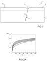
- Figure 1 shows schematically a wafer 1 of semiconductor material, in particular silicon carbide (SiC), comprising a substrate 2, on which an epitaxial layer 3, having a top surface 3a, is grown, in particular with a homo-epitaxial process.
- a defect in particular a TSD, designated by 4, propagates starting from the substrate 2 (as indicated by the arrow) towards the overlying epitaxial layer 3, generating, on its top surface 3a, a surface pit 5.
- the presence of the surface pit 5, in particular if in the active area of a corresponding power device, for example a diode or MOSFET, formed in the epitaxial layer 3, may lead to a drop in the performance and reliability of the power device; for example, the surface pit 5 may jeopardise proper growth of subsequent layers on the top surface 3a of the epitaxial layer 3, for example a dielectric layer grown via surface oxidation and/or a conductive layer designed for formation of electrodes of the power device, thus jeopardising reliability of the power device.
- Figures 2A and 2B show plots of the leakage current I leak as the reverse-biasing voltage V r increases for a power device (in this case, a Schottky diode) made starting from a silicon carbide substrate, in the case where nano-pits are present in the active area as a result of the propagation of dislocations from the substrate ( Figure 2A ), and in the case where there are dislocations, but these dislocations do not entail the presence of surface pits ( Figure 2B ). From an examination of Figures 2A and 2B it is evident that the leakage current is sensibly higher in the presence of surface pits in the active area, as compared to the case where, even in the presence of dislocations through the substrate, surface pits are not present.
- a power device in this case, a Schottky diode
- US 2017/121850 A1 discloses a method for manufacturing a silicon carbide semiconductor device, which includes: forming a silicon carbide epitaxial film on a silicon carbide substrate; flattening a surface of the epitaxial film by using chemical mechanical polishing such that the surface of the epitaxial film has an arithmetic mean roughness Ra of 0.3 nm or less; thermally oxidizing the surface of the epitaxial film to form a sacrificial oxide; removing the sacrificial oxide; and cleaning, by using deionized water, a surface of the epitaxial film exposed by the removing of the sacrificial oxide.
- WO 2017/212971 A1 discloses a polishing liquid and method for producing a polished article.
- This polishing liquid contains permanganate ions, a weak acid and a soluble salt of the weak acid.
- SiC MOS characteristics depend on the gate oxide fabrication process, and are improved by the increase of dry oxidation temperature and the applying of N2O and H2 POAs.
- the document shows that predominant origins of SiC MOS reliability degradation are wafer-related defects such as dislocation and surface defects of epitaxial layer.
- the planarization of SiC epitaxial layer surface using a CMP treatment is disclosed as an effective technique for the improvement of SiC MOS reliability.
- the aim of the present solution is to provide a process for manufacturing a silicon carbide semiconductor device, which will enable the disadvantages highlighted previously to be overcome.
- an aspect of the present solution instead of following the approach of known solutions acting on stopping or reducing propagation of defects (in particular, TSDs), envisages intervening on reducing the morphological damage generated on the surface by propagation of the same defects, in particular on reducing the pits (nano-pits) generated on the epitaxial layer surface.
- the solution proposed allows to improve subsequent processing operations envisaged by the manufacturing process on the epitaxial layer, for example an oxidation step for the growth of a dielectric layer on the epitaxial layer, preventing effects of electrical-field crowding and ensuring a uniform oxidation.
- an additional CMP step is introduced into the manufacturing process, i.e., a step of chemical-mechanical polishing of the surface of the epitaxial layer formed on the silicon carbide substrate.
- said CMP process step uses a polishing compound free of particles and having a pH lower than 5.
- This process step with the associated surface machining (which is a combination of chemical etching and mechanical planarization) enables removal of a thin superficial layer of material (of the order of hundreds of nanometres starting from the surface of the epitaxial layer), consequently making the surface of the epitaxial layer substantially free of pits.
- the pits due to propagation of the TSDs are substantially removed entirely with removal of the aforesaid superficial layer of material.
- a process for manufacturing a generic silicon carbide semiconductor device for example a power device (such as a diode or a MOSFET) is now described.
- the process first envisages providing a wafer 21 of silicon carbide (in particular 4H-SiC), comprising a substrate 22 (which is illustrated schematically in Figure 4A ).
- a wafer 21 of silicon carbide in particular 4H-SiC
- a substrate 22 which is illustrated schematically in Figure 4A
- an epitaxial growth is carried out, for example with Chemical Vapour Deposition (CVD), for the formation, on the substrate 22, of an epitaxial layer (once again of 4H-SiC) 23, having a top surface 23a.
- CVD Chemical Vapour Deposition
- a defect in particular a TSD, designated as a whole by 24 in Figure 4A , during epitaxial growth may propagate starting from the substrate 22 towards the overlying epitaxial layer 23, generating, on its top surface 23a, a surface pit 25, which may, for example, have a diameter of some nanometres (for example, less than 30 nm) .
- the manufacturing process comprises, following upon the aforesaid step of epitaxial growth (in particular, immediately after), an additional step, designated by 14 in Figure 3 , of Chemical Mechanical Polishing (CMP) using a polishing compound free of particles and having a pH less than 5, so-called "soft", of the top surface 23a of the epitaxial layer 23 formed on the substrate 22.
- CMP Chemical Mechanical Polishing
- the CMP process is preceded by a step, designated by 15, of cleaning of the wafer surface, in particular of the top surface 23a of the aforesaid epitaxial layer 23; cleaning is, for example, obtained via a jet of water at a high pressure and drying of the surface via rotation of the sample, or, alternatively via the use of chemical agents, such as HF, NH 4 OH, H 2 O 2 , HCl.
- cleaning is, for example, obtained via a jet of water at a high pressure and drying of the surface via rotation of the sample, or, alternatively via the use of chemical agents, such as HF, NH 4 OH, H 2 O 2 , HCl.
- the CMP process via combination of chemical and mechanical effects, causes removal of a thin surface layer of the epitaxial layer 23, starting from its top surface 23a, so as to remove the surface pits 25 originated by propagation of the TSDs 24, consequently making the resulting top surface of the epitaxial layer 23, designated by 23a', substantially planar and free of defects.
- the thickness of the surface layer removed (considered in a direction orthogonal to the aforesaid top surface 23a) may be comprised between 100 nm and 500 nm, for example 300 nm, it being in any case sufficient to remove, as mentioned previously, the surface pits 25, possibly entirely.
- the actual thickness of the removed surface layer will result from a compromise between the desire to remove as little material as possible (so as to optimize times and costs of the manufacturing process) and, at the same time, assure a complete removal of the surface defectiveness.
- the present Applicant has found that removal of a layer of a thickness of 100 nm may in general be sufficient to make the top surface 23a' resulting from the CMP process uniform. However, it may be convenient to remove a greater thickness, for example of 300 nm, in order to have a higher certainty that the desired results are obtained.
- the CMP process has the further advantage of reducing the surface roughness of the aforesaid resulting top surface 23a' of the epitaxial layer 23.
- the typical roughness (generally denoted as parameter Rq) measured on the top surface of an epitaxial layer is variable between 0.1 nm and 1 nm; moreover, there frequently arises a phenomenon known as "step bunching", i.e., of formation of surface steps, basically due to CVD epitaxial growth on "off-axis" substrates.
- the present Applicant has found that the aforesaid CMP process enables a marked reduction of the roughness value of the resulting top surface 23a', with values of the Rq parameter of even less than 0.1 nm (i.e., values comparable with the noise of the instrumentation used for detecting the same thickness), and moreover enables complete elimination of the step-bunching phenomenon.
- the resulting top surface 23a' is optimized and prepared for the subsequent chemical and/or mechanical processing steps, which may be envisaged for manufacturing of an electronic device (for example, a power device, such as a diode or a MOSFET).
- an electronic device for example, a power device, such as a diode or a MOSFET.
- the manufacturing process envisages, following the aforesaid CMP process, a step, designated by 16, of cleaning of the resulting top surface 23a' of the epitaxial layer, in particular via C 6 H 8 O 7 and H 2 O 2 , and subsequently a standard process of oxidation of the same resulting top surface 23a', for formation of an oxide layer on the epitaxial layer 23.
- the physical/chemical properties of the formed oxide layer are optimized thanks to the absence of defects and to the low roughness of the starting surface (the aforesaid resulting top surface 23a').
- the manufacturing process may then proceed with processing operations (known and not described in detail herein) required for formation of the desired power device, for example steps of formation and definition of conductive layers for providing electrodes, formation of passivation layers, etc.
- the present Applicant has moreover found that it is possible to configure appropriately the CMP process (in particular, in terms of the process parameters and in terms of the used consumables), so that the same CMP process will not cause defects, such as scratches or the like, on the resulting top surface 23a' of the epitaxial layer 23.
- Figure 5 shows a system 30 for implementation of the CMP process on the silicon carbide wafer, again designated by 21, which has already undergone the step of epitaxial growth for formation of the epitaxial layer 23 on the corresponding substrate 22.
- the system 30 comprises a polishing pad 32 carried by a rotating support 33, which causes rotation thereof at a certain speed; the wafer 21 is set in contact with the polishing pad 32 by a supporting head 34 (to which it is attached by a fixing layer 35); the supporting head 34, in addition to rotating about its axis of rotation, exerts a force to press the wafer 21 on the polishing pad 32.
- a polishing compound (so-called "slurry") 36 is made to flow over the surface of the polishing pad 32 so as to come into contact, thanks to rotation of the same polishing pad 32, with the wafer 21 in order to abrade its surface and cause chemical etching thereof.
- a conditioner pad 37 supported in cantilever fashion above the surface of the polishing pad 32, implements cleaning of the polishing pad 32 to clean it from residues possibly trapped on its surface and consequently to prevent any scratching of the wafer 21.
- the present Applicant has found experimentally that it is possible to achieve better electrical and physical characteristics after the CMP process, using a particle-free polishing compound 35 having a pH ⁇ 5.
- a pressure P exerted by the supporting head 34 on the polishing pad 32 comprised between 1 and 3 psi has been found to be optimal, as likewise a temperature T of the CMP process lower than 50°C, 1 psi being approximately 6.895 kPa.
- the process described enables, by introduction of the CMP process step subsequent to epitaxial growth, removal of the surface defects and therefore optimal preparation of the resulting top surface of the wafer for the subsequent processing operations for manufacturing of the semiconductor device (for example, enabling an increase in the robustness of oxide layers subsequently grown on the epitaxial layer).
- the aforesaid CMP process enables elimination of surface pits due to propagation of the dislocations coming from the substrate generated during the step of epitaxial growth. Furthermore, the CMP process has the further advantage of reducing the surface roughness and in particular the so-called step-bunching phenomenon.
- the surface roughness of the resulting top surface 23a' following upon CMP has low values, in particular with values of the Rq parameter of less than 0.5 nm, preferably less than 0.2 nm, and even more preferably less than 0.1 nm.
- the aforesaid CMP process may be configured so as not to cause scratches or surface defects, as discussed previously and as demonstrated by the experimental tests conducted by the present Applicant.
- the present solution enables an increase in the electrical yield associated to the manufacturing process, a saving in manufacturing costs, and moreover a saving of area.
- the process described may find advantageous application for any device (diodes, MOSFETs, etc.) obtained starting from a silicon carbide (SiC) substrate, on which an epitaxial growth is carried out during the processing steps envisaged for manufacturing of the same device.
- a silicon carbide (SiC) substrate on which an epitaxial growth is carried out during the processing steps envisaged for manufacturing of the same device.
Landscapes
- Mechanical Treatment Of Semiconductor (AREA)
- Recrystallisation Techniques (AREA)
- Carbon And Carbon Compounds (AREA)
- Finish Polishing, Edge Sharpening, And Grinding By Specific Grinding Devices (AREA)
Description
- The present solution relates to a process for manufacturing a silicon carbide semiconductor device having improved characteristics.
- Electronic semiconductor devices are known, for example diodes or MOSFETs (Metal Oxide Semiconductor Field-Effect Transistors), in particular for electronic power applications, made starting from a silicon carbide substrate.
- The above devices prove advantageous thanks to the favourable chemico-physical properties of silicon carbide. For instance, silicon carbide generally has a wider bandgap than silicon, which is commonly used in electronic power devices. Consequently, also with relatively small thicknesses, silicon carbide has a breakdown voltage higher than that of silicon and may therefore be advantageously used in high-voltage, high-power, and high-temperature applications.
- Manufacturing of a silicon carbide semiconductor device is, however, affected by some problems.
- For instance, problems of crystallographic quality of silicon carbide may represent an obstacle to achieving high production yields, which in general prove lower than similar devices obtained starting from silicon, consequently causing an increase in the production costs.
- In particular, epitaxial processes generally used for device manufacturing tend to propagate crystallographic defects buried in the starting substrate towards the surface of the grown epitaxial layers.
- In detail, propagation of TSDs (Threading-Screw Dislocations) from the substrate towards the epitaxial layer may generate, on the surface of the same epitaxial layer, pits or nano-pits (i.e., pits having nanometric dimensions, with a diameter of few nanometres, for example less than 30 nm) .
- It has been shown that the presence of such defects entails a reduction of the device electrical performance and in particular a drop in reliability, with a consequent reduction of the yield after electrical testing, with possible generation of high leakage currents in conditions of reverse biasing.
- The aforesaid problems are particularly important for certain applications, in particular in the automotive field, where extremely low percentages of failure are allowed (for example, less than 10) during effective use of the devices (in the example, on board a motor vehicle).
-
Figure 1 shows schematically a wafer 1 of semiconductor material, in particular silicon carbide (SiC), comprising asubstrate 2, on which anepitaxial layer 3, having atop surface 3a, is grown, in particular with a homo-epitaxial process. A defect, in particular a TSD, designated by 4, propagates starting from the substrate 2 (as indicated by the arrow) towards the overlyingepitaxial layer 3, generating, on itstop surface 3a, asurface pit 5. - The presence of the
surface pit 5, in particular if in the active area of a corresponding power device, for example a diode or MOSFET, formed in theepitaxial layer 3, may lead to a drop in the performance and reliability of the power device; for example, thesurface pit 5 may jeopardise proper growth of subsequent layers on thetop surface 3a of theepitaxial layer 3, for example a dielectric layer grown via surface oxidation and/or a conductive layer designed for formation of electrodes of the power device, thus jeopardising reliability of the power device. - Studies and experimental test - see, for example, T. Kimoto, "Material science and device physics in SiC technology for high-voltage power devices", Japanese Journal of Applied Physics 54, 040103 (2015) - have confirmed that the presence of the aforesaid surface pits (nano-pits), originating from propagation of dislocations from the substrate, effectively jeopardises device performance.
- In this regard,
Figures 2A and2B show plots of the leakage current Ileak as the reverse-biasing voltage Vr increases for a power device (in this case, a Schottky diode) made starting from a silicon carbide substrate, in the case where nano-pits are present in the active area as a result of the propagation of dislocations from the substrate (Figure 2A ), and in the case where there are dislocations, but these dislocations do not entail the presence of surface pits (Figure 2B ). From an examination ofFigures 2A and2B it is evident that the leakage current is sensibly higher in the presence of surface pits in the active area, as compared to the case where, even in the presence of dislocations through the substrate, surface pits are not present. - Solutions that have so far been proposed to overcome the problem highlighted (see, for example, N. Piluso, A. Campione, S. Lorenti, A. Severino, G. Arena, S. Coffa, F. La Via, "High Quality 4H-SiC Epitaxial Layer by Tuning CVD Process", Materials Science Forum, ISSN: 1662-9752, Vol. 963, pp. 91-96), and in particular for reducing the effect of defects on the surface of the epitaxial layer, envisage appropriate steps aimed at improving the epitaxial growth performed starting from the silicon carbide substrate. However, since TSDs are defects of a crystallographic nature, it is not possible to prevent propagation thereof towards the epitaxial layer.
- Other known solutions (see, for example, N. Piluso, A. Severino, R. Anzalone, M.A. Di Stefano, E. Fontana, M. Salanitri, S. Lorenti, A. Campione, P. Fiorenza, F. La Via, "Growth of 4H-SiC Epitaxial Layer through Optimization of Buffer Layer", Materials Science Forum, ISSN: 1662-9752, Vol. 924, pp. 84-87) envisage introduction of buffer layers, interposed between the substrate and the epitaxial layer; however, also these solutions enable at most a limited reduction of the density of dislocations, but do not arrest propagation of the same dislocations towards the surface of the epitaxial layer.
-
US 2017/121850 A1 discloses a method for manufacturing a silicon carbide semiconductor device, which includes: forming a silicon carbide epitaxial film on a silicon carbide substrate; flattening a surface of the epitaxial film by using chemical mechanical polishing such that the surface of the epitaxial film has an arithmetic mean roughness Ra of 0.3 nm or less; thermally oxidizing the surface of the epitaxial film to form a sacrificial oxide; removing the sacrificial oxide; and cleaning, by using deionized water, a surface of the epitaxial film exposed by the removing of the sacrificial oxide. -
WO 2017/212971 A1 discloses a polishing liquid and method for producing a polished article. This polishing liquid contains permanganate ions, a weak acid and a soluble salt of the weak acid. - SENZAKI J. et AI., "Challenges of high-performance and high-reliability in SiC MOS structures", Materials Science Forum, Trans Tech Publications Ltd- Switzerland, CH, vol. 717-720, pages 703 - 708, discloses the influences of wafer-related defect and gate oxide fabrication process on characteristics of SiC MOS power devices. The SiC MOS characteristics depend on the gate oxide fabrication process, and are improved by the increase of dry oxidation temperature and the applying of N2O and H2 POAs. In addition, the document shows that predominant origins of SiC MOS reliability degradation are wafer-related defects such as dislocation and surface defects of epitaxial layer. Moreover, the planarization of SiC epitaxial layer surface using a CMP treatment is disclosed as an effective technique for the improvement of SiC MOS reliability.
- The need is therefore certainly felt to provide a solution that will enable reduction of the disadvantages linked to propagation of the crystallographic defects, in particular TSDs, towards the surface of the epitaxial layer grown on the silicon carbide substrate.
- The aim of the present solution is to provide a process for manufacturing a silicon carbide semiconductor device, which will enable the disadvantages highlighted previously to be overcome.
- According to the present invention, a manufacturing process is consequently provided, as defined in the appended claims.
- For a better understanding of the present invention, preferred embodiments thereof are now described, purely by way of non-limiting example and with reference to the attached drawings, wherein:
-
Figure 1 is a schematic and simplified cross-sectional view of a portion of a silicon carbide semiconductor device; -
Figures 2A and2B show plots of leakage currents in the semiconductor device, associated to the presence of surface defects; -
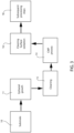
Figure 3 shows a simplified flowchart of operations according to a process for manufacturing a silicon carbide semiconductor device according to the present solution; -
Figures 4A and 4B are a schematic and simplified cross-sectional views of a portion of a silicon carbide semiconductor device, during respective steps of the manufacturing process according to the present solution; and -
Figure 5 is a schematic representation of a CMP (Chemical Mechanical Polishing) system, used during a process for manufacturing a silicon carbide semiconductor device according to the present solution. - As will be discussed in detail in what follows, an aspect of the present solution, instead of following the approach of known solutions acting on stopping or reducing propagation of defects (in particular, TSDs), envisages intervening on reducing the morphological damage generated on the surface by propagation of the same defects, in particular on reducing the pits (nano-pits) generated on the epitaxial layer surface.
- The solution proposed allows to improve subsequent processing operations envisaged by the manufacturing process on the epitaxial layer, for example an oxidation step for the growth of a dielectric layer on the epitaxial layer, preventing effects of electrical-field crowding and ensuring a uniform oxidation.
- According to the present solution, an additional CMP step is introduced into the manufacturing process, i.e., a step of chemical-mechanical polishing of the surface of the epitaxial layer formed on the silicon carbide substrate. According to the present invention, said CMP process step uses a polishing compound free of particles and having a pH lower than 5.
- This process step, with the associated surface machining (which is a combination of chemical etching and mechanical planarization) enables removal of a thin superficial layer of material (of the order of hundreds of nanometres starting from the surface of the epitaxial layer), consequently making the surface of the epitaxial layer substantially free of pits. The pits due to propagation of the TSDs are substantially removed entirely with removal of the aforesaid superficial layer of material.
- With reference to
Figure 3 , a process for manufacturing a generic silicon carbide semiconductor device, for example a power device (such as a diode or a MOSFET) is now described. - As indicated at
step 10, the process first envisages providing awafer 21 of silicon carbide (in particular 4H-SiC), comprising a substrate 22 (which is illustrated schematically inFigure 4A ). Next (step 11), an epitaxial growth is carried out, for example with Chemical Vapour Deposition (CVD), for the formation, on thesubstrate 22, of an epitaxial layer (once again of 4H-SiC) 23, having atop surface 23a. - As discussed previously, a defect, in particular a TSD, designated as a whole by 24 in
Figure 4A , during epitaxial growth may propagate starting from thesubstrate 22 towards the overlyingepitaxial layer 23, generating, on itstop surface 23a, asurface pit 25, which may, for example, have a diameter of some nanometres (for example, less than 30 nm) . - According to the present solution, the manufacturing process comprises, following upon the aforesaid step of epitaxial growth (in particular, immediately after), an additional step, designated by 14 in
Figure 3 , of Chemical Mechanical Polishing (CMP) using a polishing compound free of particles and having a pH less than 5, so-called "soft", of thetop surface 23a of theepitaxial layer 23 formed on thesubstrate 22. - As indicated again in
Figure 3 , the CMP process is preceded by a step, designated by 15, of cleaning of the wafer surface, in particular of thetop surface 23a of the aforesaidepitaxial layer 23; cleaning is, for example, obtained via a jet of water at a high pressure and drying of the surface via rotation of the sample, or, alternatively via the use of chemical agents, such as HF, NH4OH, H2O2, HCl. - As illustrated schematically in
Figure 4B , the CMP process, via combination of chemical and mechanical effects, causes removal of a thin surface layer of theepitaxial layer 23, starting from itstop surface 23a, so as to remove thesurface pits 25 originated by propagation of theTSDs 24, consequently making the resulting top surface of theepitaxial layer 23, designated by 23a', substantially planar and free of defects. - In detail, the thickness of the surface layer removed (considered in a direction orthogonal to the
aforesaid top surface 23a) may be comprised between 100 nm and 500 nm, for example 300 nm, it being in any case sufficient to remove, as mentioned previously, thesurface pits 25, possibly entirely. - As it will be clear, the actual thickness of the removed surface layer will result from a compromise between the desire to remove as little material as possible (so as to optimize times and costs of the manufacturing process) and, at the same time, assure a complete removal of the surface defectiveness. The present Applicant has found that removal of a layer of a thickness of 100 nm may in general be sufficient to make the
top surface 23a' resulting from the CMP process uniform. However, it may be convenient to remove a greater thickness, for example of 300 nm, in order to have a higher certainty that the desired results are obtained. - In any case, the CMP process has the further advantage of reducing the surface roughness of the aforesaid resulting
top surface 23a' of theepitaxial layer 23. - In this regard, it is known that the typical roughness (generally denoted as parameter Rq) measured on the top surface of an epitaxial layer is variable between 0.1 nm and 1 nm; moreover, there frequently arises a phenomenon known as "step bunching", i.e., of formation of surface steps, basically due to CVD epitaxial growth on "off-axis" substrates.
- The present Applicant has found that the aforesaid CMP process enables a marked reduction of the roughness value of the resulting
top surface 23a', with values of the Rq parameter of even less than 0.1 nm (i.e., values comparable with the noise of the instrumentation used for detecting the same thickness), and moreover enables complete elimination of the step-bunching phenomenon. - Basically, the resulting
top surface 23a', after the CMP process, is optimized and prepared for the subsequent chemical and/or mechanical processing steps, which may be envisaged for manufacturing of an electronic device (for example, a power device, such as a diode or a MOSFET). - In this regard, with reference again to
Figure 3 , the manufacturing process envisages, following the aforesaid CMP process, a step, designated by 16, of cleaning of the resultingtop surface 23a' of the epitaxial layer, in particular via C6H8O7 and H2O2, and subsequently a standard process of oxidation of the same resultingtop surface 23a', for formation of an oxide layer on theepitaxial layer 23. - Advantageously, the physical/chemical properties of the formed oxide layer are optimized thanks to the absence of defects and to the low roughness of the starting surface (the aforesaid resulting
top surface 23a'). - As indicated generically at
step 18, the manufacturing process may then proceed with processing operations (known and not described in detail herein) required for formation of the desired power device, for example steps of formation and definition of conductive layers for providing electrodes, formation of passivation layers, etc. - It will thus be noted that the proposed solution differ from pre-existing solutions substantially for the fact of envisaging the additional CMP process step (with standard preliminary cleaning and subsequent dedicated cleaning), therefore not involving a substantial increase in terms of costs or times of the manufacturing process.
- The present Applicant has moreover found that it is possible to configure appropriately the CMP process (in particular, in terms of the process parameters and in terms of the used consumables), so that the same CMP process will not cause defects, such as scratches or the like, on the resulting
top surface 23a' of theepitaxial layer 23. - In this regard,
Figure 5 shows asystem 30 for implementation of the CMP process on the silicon carbide wafer, again designated by 21, which has already undergone the step of epitaxial growth for formation of theepitaxial layer 23 on thecorresponding substrate 22. - In particular, the
system 30 comprises apolishing pad 32 carried by arotating support 33, which causes rotation thereof at a certain speed; thewafer 21 is set in contact with thepolishing pad 32 by a supporting head 34 (to which it is attached by a fixing layer 35); the supportinghead 34, in addition to rotating about its axis of rotation, exerts a force to press thewafer 21 on thepolishing pad 32. - A polishing compound (so-called "slurry") 36 is made to flow over the surface of the
polishing pad 32 so as to come into contact, thanks to rotation of thesame polishing pad 32, with thewafer 21 in order to abrade its surface and cause chemical etching thereof. - Moreover, a
conditioner pad 37 supported in cantilever fashion above the surface of thepolishing pad 32, implements cleaning of thepolishing pad 32 to clean it from residues possibly trapped on its surface and consequently to prevent any scratching of thewafer 21. - The present Applicant has found experimentally that it is possible to achieve better electrical and physical characteristics after the CMP process, using a particle-
free polishing compound 35 having a pH < 5. - In addition, a pressure P exerted by the supporting
head 34 on thepolishing pad 32 comprised between 1 and 3 psi has been found to be optimal, as likewise a temperature T of the CMP process lower than 50°C, 1 psi being approximately 6.895 kPa. - The present Applicant has moreover found that using one or more of the following further parameters of the CMP process is advantageous: rate of rotation of the
polishing pad 32 less than 70 rpm; rate of rotation of the supportinghead 34 less than 60 rpm; force of thrust of theconditioner pad 37 on the polishing pad approximately 6 lbf (i.e., around 3 kgf, 1kgf being approximately 29.4 N); flow of the polishingcompound 36 less than 100 ml/min. - The advantages of the proposed solution emerge clearly from the foregoing description.
- In any case, it is underlined that the process described enables, by introduction of the CMP process step subsequent to epitaxial growth, removal of the surface defects and therefore optimal preparation of the resulting top surface of the wafer for the subsequent processing operations for manufacturing of the semiconductor device (for example, enabling an increase in the robustness of oxide layers subsequently grown on the epitaxial layer).
- In particular, the aforesaid CMP process enables elimination of surface pits due to propagation of the dislocations coming from the substrate generated during the step of epitaxial growth. Furthermore, the CMP process has the further advantage of reducing the surface roughness and in particular the so-called step-bunching phenomenon. As mentioned previously, the surface roughness of the resulting
top surface 23a' following upon CMP has low values, in particular with values of the Rq parameter of less than 0.5 nm, preferably less than 0.2 nm, and even more preferably less than 0.1 nm. - Moreover, advantageously, the aforesaid CMP process may be configured so as not to cause scratches or surface defects, as discussed previously and as demonstrated by the experimental tests conducted by the present Applicant.
- Consequently, the present solution enables an increase in the electrical yield associated to the manufacturing process, a saving in manufacturing costs, and moreover a saving of area.
- In particular, it is underlined that the process described may find advantageous application for any device (diodes, MOSFETs, etc.) obtained starting from a silicon carbide (SiC) substrate, on which an epitaxial growth is carried out during the processing steps envisaged for manufacturing of the same device.
Claims (12)
- A process for manufacturing a silicon carbide semiconductor device, comprising:providing a silicon carbide wafer (21), having a substrate (22); andcarrying out an epitaxial growth for formation on the substrate (22) of an epitaxial layer (23), having a top surface (23a), propagation of dislocations (24) from the substrate (22) towards the top surface (23a) occurring during said epitaxial growth with consequent formation of surface damages,further comprising, subsequent to the step of carrying out an epitaxial growth: removing a surface portion of the epitaxial layer (23) starting from said top surface (23a), so as to remove the surface damages at said top surface (23a) and define a resulting top surface (23a') substantially free of defects;wherein said surface damages are pits (25) due to propagation of the dislocations (24) starting from said substrate (22) towards said top surface (23a) during said epitaxial growth;and wherein the step of removing comprises carrying out a step of Chemical Mechanical Polishing - CMP - of the top surface (23a) of the epitaxial layer (23);characterized in that said CMP step is carried out using a polishing compound (36) free of particles and having a pH lower than 5.
- The process according to claim 1, wherein the removed surface portion of the epitaxial layer (23) has a thickness comprised between 100 nm and 500 nm.
- The process according to claim 2, wherein said thickness is equal to 300 nm.
- The process according to any of the preceding claims, wherein, during said CMP step, the wafer (21) is pressed against a polishing pad (32) by a supporting head (34) with a pressure (P) comprised between 6.9 and 20.7 kPa (1 and 3 psi).
- The process according to claim 4, wherein said CMP step is moreover carried out with one or more of the following parameters: rate of rotation of the polishing pad (32) < 70 rpm; rate of rotation of the supporting head (34) < 60 rpm; force of thrust of the supporting head (34) on the polishing pad (32) about 29.4 N (3 kgf); flow of the polishing compound (36) < 100 ml/min.
- The process according to any of the preceding claims, wherein said CMP step is carried out at a temperature (T) lower than 50°C.
- The process according to any of the preceding claims, further comprising: prior to said CMP step, cleaning of the top surface (23a) of the epitaxial layer (23); and moreover, subsequent to said CMP step, a dedicated washing of the resulting top surface (23a'); wherein, following upon said CMP step and said dedicated washing, the resulting top surface (23a') has a value of roughness (Rq) lower than 0.1 nm.
- The process according to any of the preceding claims, wherein said epitaxial growth is carried out with Chemical Vapour Deposition - CVD.
- The process according to any of the preceding claims, wherein said epitaxial layer (23) is made of 4H-SiC.
- The process according to any of the preceding claims, further comprising, following upon the step of removing a surface portion of the epitaxial layer (23), carrying out further processing operations starting from the resulting top surface (23a') to form said semiconductor device.
- The process according to any of the preceding claims, wherein said semiconductor device is an electronic power device.
- The process according to claim 11, wherein said electronic power device is a diode or a MOSFET.
Applications Claiming Priority (1)
| Application Number | Priority Date | Filing Date | Title |
|---|---|---|---|
| IT102020000016279A IT202000016279A1 (en) | 2020-07-06 | 2020-07-06 | PROCESS FOR MANUFACTURING A SILICON CARBIDE SEMICONDUCTOR DEVICE WITH IMPROVED CHARACTERISTICS |
Publications (3)
| Publication Number | Publication Date |
|---|---|
| EP3937209A1 EP3937209A1 (en) | 2022-01-12 |
| EP3937209B1 true EP3937209B1 (en) | 2024-12-18 |
| EP3937209C0 EP3937209C0 (en) | 2024-12-18 |
Family
ID=72356438
Family Applications (1)
| Application Number | Title | Priority Date | Filing Date |
|---|---|---|---|
| EP21183643.2A Active EP3937209B1 (en) | 2020-07-06 | 2021-07-05 | Process for manufacturing a silicon carbide semiconductor device having improved characteristics |
Country Status (5)
| Country | Link |
|---|---|
| US (1) | US12635439B2 (en) |
| EP (1) | EP3937209B1 (en) |
| JP (1) | JP2022014457A (en) |
| CN (1) | CN114300352B (en) |
| IT (1) | IT202000016279A1 (en) |
Family Cites Families (24)
| Publication number | Priority date | Publication date | Assignee | Title |
|---|---|---|---|---|
| JP3259225B2 (en) | 1999-12-27 | 2002-02-25 | 株式会社ニコン | Polishing status monitoring method and apparatus, polishing apparatus, process wafer, semiconductor device manufacturing method, and semiconductor device |
| US7230274B2 (en) | 2004-03-01 | 2007-06-12 | Cree, Inc | Reduction of carrot defects in silicon carbide epitaxy |
| EP1619276B1 (en) * | 2004-07-19 | 2017-01-11 | Norstel AB | Homoepitaxial growth of SiC on low off-axis SiC wafers |
| DE102005024073A1 (en) | 2005-05-25 | 2006-11-30 | Siltronic Ag | Semiconductor layer structure and method for producing a semiconductor layer structure |
| TWI332017B (en) | 2005-12-26 | 2010-10-21 | Hitachi Chemical Co Ltd | Abrasive-free polishing slurry and cmp process |
| EP2394787B1 (en) | 2009-02-04 | 2019-05-29 | Hitachi Metals, Ltd. | Manufacturing method for a silicon carbide monocrystal substrate |
| JP5267177B2 (en) | 2009-02-04 | 2013-08-21 | 日立金属株式会社 | Method for manufacturing silicon carbide single crystal substrate |
| JP4959763B2 (en) | 2009-08-28 | 2012-06-27 | 昭和電工株式会社 | SiC epitaxial wafer and manufacturing method thereof |
| WO2011058830A1 (en) | 2009-11-13 | 2011-05-19 | 住友電気工業株式会社 | Method for manufacturing a semiconductor substrate |
| US20110221039A1 (en) | 2010-03-12 | 2011-09-15 | Sinmat, Inc. | Defect capping for reduced defect density epitaxial articles |
| CN104979184B (en) * | 2011-10-07 | 2018-02-02 | 旭硝子株式会社 | Monocrystalline silicon carbide substrate and lapping liquid |
| JP6113960B2 (en) * | 2012-02-21 | 2017-04-12 | 株式会社荏原製作所 | Substrate processing apparatus and substrate processing method |
| DE102013010187B4 (en) | 2012-06-27 | 2024-11-28 | Fairchild Semiconductor Corp. | Schottky barrier device with locally planarized surface and associated semiconductor product |
| US9312164B2 (en) * | 2014-04-13 | 2016-04-12 | Texas Instruments Incorporated | Localized region of isolated silicon over dielectric mesa |
| US20160020246A1 (en) | 2014-07-15 | 2016-01-21 | United Microelectronics Corporation | Method for fabricating cmos image sensors and surface treating process thereof |
| JP2016127177A (en) | 2015-01-06 | 2016-07-11 | 住友電気工業株式会社 | Silicon carbide substrate, silicon carbide semiconductor device and silicon carbide substrate manufacturing method |
| JP6361747B2 (en) * | 2015-02-02 | 2018-07-25 | 富士電機株式会社 | Silicon carbide semiconductor device manufacturing method and silicon carbide semiconductor device |
| WO2016185819A1 (en) | 2015-05-18 | 2016-11-24 | 住友電気工業株式会社 | Method for manufacturing silicon carbide epitaxial substrate, silicon carbide epitaxial substrate, method for manufacturing silicon carbide semiconductor device, and silicon carbide semiconductor device |
| WO2017212971A1 (en) * | 2016-06-08 | 2017-12-14 | 三井金属鉱業株式会社 | Polishing liquid and method for producing polished article |
| US10811500B2 (en) * | 2017-01-31 | 2020-10-20 | Sumitomo Electric Industries, Ltd. | Silicon carbide epitaxial substrate and method for manufacturing silicon carbide semiconductor device |
| US11078380B2 (en) | 2017-07-10 | 2021-08-03 | Entegris, Inc. | Hard abrasive particle-free polishing of hard materials |
| US11638978B2 (en) * | 2019-06-10 | 2023-05-02 | Rohm And Haas Electronic Materials Cmp Holdings, Inc. | Low-debris fluopolymer composite CMP polishing pad |
| EP4066275B1 (en) * | 2019-11-29 | 2023-12-27 | Soitec | Method for manufacturing a composite structure comprising a thin layer of monocrystalline sic on an sic carrier substrate |
| JP7275393B2 (en) * | 2020-06-24 | 2023-05-17 | 三菱電機株式会社 | Semiconductor device and its manufacturing method |
-
2020
- 2020-07-06 IT IT102020000016279A patent/IT202000016279A1/en unknown
-
2021
- 2021-07-05 EP EP21183643.2A patent/EP3937209B1/en active Active
- 2021-07-06 CN CN202110762512.1A patent/CN114300352B/en active Active
- 2021-07-06 JP JP2021112177A patent/JP2022014457A/en active Pending
- 2021-07-06 US US17/368,437 patent/US12635439B2/en active Active
Also Published As
| Publication number | Publication date |
|---|---|
| CN114300352B (en) | 2026-03-27 |
| US12635439B2 (en) | 2026-05-19 |
| US20220005702A1 (en) | 2022-01-06 |
| CN114300352A (en) | 2022-04-08 |
| JP2022014457A (en) | 2022-01-19 |
| EP3937209A1 (en) | 2022-01-12 |
| IT202000016279A1 (en) | 2022-01-06 |
| EP3937209C0 (en) | 2024-12-18 |
Similar Documents
| Publication | Publication Date | Title |
|---|---|---|
| KR100394972B1 (en) | Epitaxially coated semiconductor wafer and process for producing it | |
| Deng et al. | Plasma-assisted polishing of gallium nitride to obtain a pit-free and atomically flat surface | |
| US9449814B2 (en) | Manufacturing method of semiconductor device | |
| KR101905788B1 (en) | Method for finishing a substrate of the semiconductor-on-insulator type | |
| US9287353B2 (en) | Composite substrate and method of manufacturing the same | |
| US6338805B1 (en) | Process for fabricating semiconductor wafers with external gettering | |
| US6376335B1 (en) | Semiconductor wafer manufacturing process | |
| KR20100033414A (en) | Bonded wafer manufacturing method | |
| WO2011106144A1 (en) | Methods for reducing the width of the unbonded region in soi structures and wafers and soi structures produced by such methods | |
| WO2018216203A1 (en) | Gaas substrate and production method therefor | |
| KR20110052456A (en) | Wafer Bonding Method | |
| KR102138949B1 (en) | Method for producing sos substrates, and sos substrate | |
| JP2023528784A (en) | Temporary strippable substrate for very high temperatures and process for transferring working layer from said substrate | |
| JP5529217B2 (en) | Manufacturing method of semiconductor device | |
| JPWO2016125404A1 (en) | Silicon carbide semiconductor device manufacturing method and silicon carbide semiconductor device | |
| WO2001049450A1 (en) | Chemical mechanical polishing process for manufacturing dopant-striation-free silicon wafers | |
| US12635439B2 (en) | Process for manufacturing a silicon carbide semiconductor device having improved characteristics | |
| JP3450683B2 (en) | Preparation method of semiconductor processing surface | |
| WO2007063677A1 (en) | Method for grinding surface of semiconductor wafer and method for manufacturing semiconductor wafer | |
| JP6199354B2 (en) | Manufacturing method of semiconductor device | |
| KR102507136B1 (en) | Method for reducing the metal contamination on a surface of a substrate | |
| US20260018457A1 (en) | Methods of processing semiconductor-on-insulator structures using clean-and-etch operation | |
| US6248651B1 (en) | Low cost method of fabricating transient voltage suppressor semiconductor devices or the like | |
| JP5809317B2 (en) | Manufacturing method of semiconductor device | |
| CN120824187A (en) | SiC backside conditioning for improved ohmic contact formation |
Legal Events
| Date | Code | Title | Description |
|---|---|---|---|
| PUAI | Public reference made under article 153(3) epc to a published international application that has entered the european phase |
Free format text: ORIGINAL CODE: 0009012 |
|
| STAA | Information on the status of an ep patent application or granted ep patent |
Free format text: STATUS: THE APPLICATION HAS BEEN PUBLISHED |
|
| AK | Designated contracting states |
Kind code of ref document: A1 Designated state(s): AL AT BE BG CH CY CZ DE DK EE ES FI FR GB GR HR HU IE IS IT LI LT LU LV MC MK MT NL NO PL PT RO RS SE SI SK SM TR |
|
| B565 | Issuance of search results under rule 164(2) epc |
Effective date: 20211108 |
|
| STAA | Information on the status of an ep patent application or granted ep patent |
Free format text: STATUS: REQUEST FOR EXAMINATION WAS MADE |
|
| 17P | Request for examination filed |
Effective date: 20220706 |
|
| RBV | Designated contracting states (corrected) |
Designated state(s): AL AT BE BG CH CY CZ DE DK EE ES FI FR GB GR HR HU IE IS IT LI LT LU LV MC MK MT NL NO PL PT RO RS SE SI SK SM TR |
|
| GRAP | Despatch of communication of intention to grant a patent |
Free format text: ORIGINAL CODE: EPIDOSNIGR1 |
|
| STAA | Information on the status of an ep patent application or granted ep patent |
Free format text: STATUS: GRANT OF PATENT IS INTENDED |
|
| INTG | Intention to grant announced |
Effective date: 20240712 |
|
| GRAS | Grant fee paid |
Free format text: ORIGINAL CODE: EPIDOSNIGR3 |
|
| GRAA | (expected) grant |
Free format text: ORIGINAL CODE: 0009210 |
|
| STAA | Information on the status of an ep patent application or granted ep patent |
Free format text: STATUS: THE PATENT HAS BEEN GRANTED |
|
| AK | Designated contracting states |
Kind code of ref document: B1 Designated state(s): AL AT BE BG CH CY CZ DE DK EE ES FI FR GB GR HR HU IE IS IT LI LT LU LV MC MK MT NL NO PL PT RO RS SE SI SK SM TR |
|
| REG | Reference to a national code |
Ref country code: CH Ref legal event code: EP |
|
| REG | Reference to a national code |
Ref country code: DE Ref legal event code: R096 Ref document number: 602021023458 Country of ref document: DE |
|
| REG | Reference to a national code |
Ref country code: IE Ref legal event code: FG4D |
|
| U01 | Request for unitary effect filed |
Effective date: 20241231 |
|
| U07 | Unitary effect registered |
Designated state(s): AT BE BG DE DK EE FI FR IT LT LU LV MT NL PT RO SE SI Effective date: 20250114 |
|
| PG25 | Lapsed in a contracting state [announced via postgrant information from national office to epo] |
Ref country code: HR Free format text: LAPSE BECAUSE OF FAILURE TO SUBMIT A TRANSLATION OF THE DESCRIPTION OR TO PAY THE FEE WITHIN THE PRESCRIBED TIME-LIMIT Effective date: 20241218 |
|
| PG25 | Lapsed in a contracting state [announced via postgrant information from national office to epo] |
Ref country code: NO Free format text: LAPSE BECAUSE OF FAILURE TO SUBMIT A TRANSLATION OF THE DESCRIPTION OR TO PAY THE FEE WITHIN THE PRESCRIBED TIME-LIMIT Effective date: 20250318 |
|
| PG25 | Lapsed in a contracting state [announced via postgrant information from national office to epo] |
Ref country code: GR Free format text: LAPSE BECAUSE OF FAILURE TO SUBMIT A TRANSLATION OF THE DESCRIPTION OR TO PAY THE FEE WITHIN THE PRESCRIBED TIME-LIMIT Effective date: 20250319 |
|
| PG25 | Lapsed in a contracting state [announced via postgrant information from national office to epo] |
Ref country code: RS Free format text: LAPSE BECAUSE OF FAILURE TO SUBMIT A TRANSLATION OF THE DESCRIPTION OR TO PAY THE FEE WITHIN THE PRESCRIBED TIME-LIMIT Effective date: 20250318 |
|
| PG25 | Lapsed in a contracting state [announced via postgrant information from national office to epo] |
Ref country code: SM Free format text: LAPSE BECAUSE OF FAILURE TO SUBMIT A TRANSLATION OF THE DESCRIPTION OR TO PAY THE FEE WITHIN THE PRESCRIBED TIME-LIMIT Effective date: 20241218 |
|
| PG25 | Lapsed in a contracting state [announced via postgrant information from national office to epo] |
Ref country code: PL Free format text: LAPSE BECAUSE OF FAILURE TO SUBMIT A TRANSLATION OF THE DESCRIPTION OR TO PAY THE FEE WITHIN THE PRESCRIBED TIME-LIMIT Effective date: 20241218 |
|
| PG25 | Lapsed in a contracting state [announced via postgrant information from national office to epo] |
Ref country code: ES Free format text: LAPSE BECAUSE OF FAILURE TO SUBMIT A TRANSLATION OF THE DESCRIPTION OR TO PAY THE FEE WITHIN THE PRESCRIBED TIME-LIMIT Effective date: 20241218 |
|
| PG25 | Lapsed in a contracting state [announced via postgrant information from national office to epo] |
Ref country code: IS Free format text: LAPSE BECAUSE OF FAILURE TO SUBMIT A TRANSLATION OF THE DESCRIPTION OR TO PAY THE FEE WITHIN THE PRESCRIBED TIME-LIMIT Effective date: 20250418 |
|
| PG25 | Lapsed in a contracting state [announced via postgrant information from national office to epo] |
Ref country code: SK Free format text: LAPSE BECAUSE OF FAILURE TO SUBMIT A TRANSLATION OF THE DESCRIPTION OR TO PAY THE FEE WITHIN THE PRESCRIBED TIME-LIMIT Effective date: 20241218 |
|
| PG25 | Lapsed in a contracting state [announced via postgrant information from national office to epo] |
Ref country code: CZ Free format text: LAPSE BECAUSE OF FAILURE TO SUBMIT A TRANSLATION OF THE DESCRIPTION OR TO PAY THE FEE WITHIN THE PRESCRIBED TIME-LIMIT Effective date: 20241218 |
|
| U20 | Renewal fee for the european patent with unitary effect paid |
Year of fee payment: 5 Effective date: 20250620 |
|
| PLBE | No opposition filed within time limit |
Free format text: ORIGINAL CODE: 0009261 |
|
| STAA | Information on the status of an ep patent application or granted ep patent |
Free format text: STATUS: NO OPPOSITION FILED WITHIN TIME LIMIT |
|
| REG | Reference to a national code |
Ref country code: CH Ref legal event code: L10 Free format text: ST27 STATUS EVENT CODE: U-0-0-L10-L00 (AS PROVIDED BY THE NATIONAL OFFICE) Effective date: 20251029 |
|
| 26N | No opposition filed |
Effective date: 20250919 |
|
| REG | Reference to a national code |
Ref country code: CH Ref legal event code: H13 Free format text: ST27 STATUS EVENT CODE: U-0-0-H10-H13 (AS PROVIDED BY THE NATIONAL OFFICE) Effective date: 20260224 |
|
| GBPC | Gb: european patent ceased through non-payment of renewal fee |
Effective date: 20250705 |
|
| PG25 | Lapsed in a contracting state [announced via postgrant information from national office to epo] |
Ref country code: GB Free format text: LAPSE BECAUSE OF NON-PAYMENT OF DUE FEES Effective date: 20250705 |
|
| PG25 | Lapsed in a contracting state [announced via postgrant information from national office to epo] |
Ref country code: CH Free format text: LAPSE BECAUSE OF NON-PAYMENT OF DUE FEES Effective date: 20250731 |
|
| PG25 | Lapsed in a contracting state [announced via postgrant information from national office to epo] |
Ref country code: IE Free format text: LAPSE BECAUSE OF NON-PAYMENT OF DUE FEES Effective date: 20250705 |
|
| PG25 | Lapsed in a contracting state [announced via postgrant information from national office to epo] |
Ref country code: MC Free format text: LAPSE BECAUSE OF FAILURE TO SUBMIT A TRANSLATION OF THE DESCRIPTION OR TO PAY THE FEE WITHIN THE PRESCRIBED TIME-LIMIT Effective date: 20241218 |
|
| U20 | Renewal fee for the european patent with unitary effect paid |
Year of fee payment: 6 Effective date: 20260618 |
|
| PG25 | Lapsed in a contracting state [announced via postgrant information from national office to epo] |
Ref country code: CY Free format text: LAPSE BECAUSE OF FAILURE TO SUBMIT A TRANSLATION OF THE DESCRIPTION OR TO PAY THE FEE WITHIN THE PRESCRIBED TIME-LIMIT Effective date: 20241218 |