JP7275393B2 - Semiconductor device and its manufacturing method - Google Patents
Semiconductor device and its manufacturing method Download PDFInfo
- Publication number
- JP7275393B2 JP7275393B2 JP2022531324A JP2022531324A JP7275393B2 JP 7275393 B2 JP7275393 B2 JP 7275393B2 JP 2022531324 A JP2022531324 A JP 2022531324A JP 2022531324 A JP2022531324 A JP 2022531324A JP 7275393 B2 JP7275393 B2 JP 7275393B2
- Authority
- JP
- Japan
- Prior art keywords
- pillar
- type
- peripheral portion
- conductivity type
- width
- Prior art date
- Legal status (The legal status is an assumption and is not a legal conclusion. Google has not performed a legal analysis and makes no representation as to the accuracy of the status listed.)
- Active
Links
- 239000004065 semiconductor Substances 0.000 title claims description 359
- 238000004519 manufacturing process Methods 0.000 title claims description 130
- 229910010271 silicon carbide Inorganic materials 0.000 claims description 348
- HBMJWWWQQXIZIP-UHFFFAOYSA-N silicon carbide Chemical compound [Si+]#[C-] HBMJWWWQQXIZIP-UHFFFAOYSA-N 0.000 claims description 346
- 230000002093 peripheral effect Effects 0.000 claims description 175
- 239000012535 impurity Substances 0.000 claims description 156
- 238000000034 method Methods 0.000 claims description 99
- 239000000758 substrate Substances 0.000 claims description 87
- 239000000463 material Substances 0.000 claims description 18
- 238000005530 etching Methods 0.000 claims description 11
- 150000002500 ions Chemical class 0.000 claims description 4
- 239000010410 layer Substances 0.000 description 308
- 230000004048 modification Effects 0.000 description 58
- 238000012986 modification Methods 0.000 description 58
- 239000011229 interlayer Substances 0.000 description 31
- 238000010586 diagram Methods 0.000 description 22
- 230000008569 process Effects 0.000 description 21
- VYPSYNLAJGMNEJ-UHFFFAOYSA-N Silicium dioxide Chemical compound O=[Si]=O VYPSYNLAJGMNEJ-UHFFFAOYSA-N 0.000 description 20
- 229910052814 silicon oxide Inorganic materials 0.000 description 20
- 239000013078 crystal Substances 0.000 description 18
- 238000005468 ion implantation Methods 0.000 description 17
- 230000005684 electric field Effects 0.000 description 15
- 230000015556 catabolic process Effects 0.000 description 12
- 208000028659 discharge Diseases 0.000 description 11
- 229910021420 polycrystalline silicon Inorganic materials 0.000 description 9
- 239000004020 conductor Substances 0.000 description 8
- 238000001312 dry etching Methods 0.000 description 8
- 229920005591 polysilicon Polymers 0.000 description 8
- 239000007789 gas Substances 0.000 description 6
- 230000015572 biosynthetic process Effects 0.000 description 5
- 230000007547 defect Effects 0.000 description 5
- 238000012545 processing Methods 0.000 description 5
- 230000004913 activation Effects 0.000 description 4
- 238000000137 annealing Methods 0.000 description 4
- 238000000059 patterning Methods 0.000 description 4
- 238000005498 polishing Methods 0.000 description 4
- XKRFYHLGVUSROY-UHFFFAOYSA-N Argon Chemical compound [Ar] XKRFYHLGVUSROY-UHFFFAOYSA-N 0.000 description 2
- IJGRMHOSHXDMSA-UHFFFAOYSA-N Atomic nitrogen Chemical compound N#N IJGRMHOSHXDMSA-UHFFFAOYSA-N 0.000 description 2
- KRHYYFGTRYWZRS-UHFFFAOYSA-N Fluorane Chemical compound F KRHYYFGTRYWZRS-UHFFFAOYSA-N 0.000 description 2
- XUIMIQQOPSSXEZ-UHFFFAOYSA-N Silicon Chemical compound [Si] XUIMIQQOPSSXEZ-UHFFFAOYSA-N 0.000 description 2
- 238000013461 design Methods 0.000 description 2
- 230000000694 effects Effects 0.000 description 2
- 239000002184 metal Substances 0.000 description 2
- 230000000149 penetrating effect Effects 0.000 description 2
- 229910052710 silicon Inorganic materials 0.000 description 2
- 239000010703 silicon Substances 0.000 description 2
- 229910052786 argon Inorganic materials 0.000 description 1
- 239000000470 constituent Substances 0.000 description 1
- 230000005669 field effect Effects 0.000 description 1
- 238000010438 heat treatment Methods 0.000 description 1
- 230000006872 improvement Effects 0.000 description 1
- 239000011261 inert gas Substances 0.000 description 1
- 238000009413 insulation Methods 0.000 description 1
- 230000010354 integration Effects 0.000 description 1
- 238000012423 maintenance Methods 0.000 description 1
- 229910052757 nitrogen Inorganic materials 0.000 description 1
- 230000003647 oxidation Effects 0.000 description 1
- 238000007254 oxidation reaction Methods 0.000 description 1
- 238000002161 passivation Methods 0.000 description 1
- SBEQWOXEGHQIMW-UHFFFAOYSA-N silicon Chemical compound [Si].[Si] SBEQWOXEGHQIMW-UHFFFAOYSA-N 0.000 description 1
- 239000002356 single layer Substances 0.000 description 1
- 239000011800 void material Substances 0.000 description 1
Images


Classifications
-
- H—ELECTRICITY
- H01—ELECTRIC ELEMENTS
- H01L—SEMICONDUCTOR DEVICES NOT COVERED BY CLASS H10
- H01L29/00—Semiconductor devices adapted for rectifying, amplifying, oscillating or switching, or capacitors or resistors with at least one potential-jump barrier or surface barrier, e.g. PN junction depletion layer or carrier concentration layer; Details of semiconductor bodies or of electrodes thereof ; Multistep manufacturing processes therefor
- H01L29/02—Semiconductor bodies ; Multistep manufacturing processes therefor
- H01L29/06—Semiconductor bodies ; Multistep manufacturing processes therefor characterised by their shape; characterised by the shapes, relative sizes, or dispositions of the semiconductor regions ; characterised by the concentration or distribution of impurities within semiconductor regions
- H01L29/0603—Semiconductor bodies ; Multistep manufacturing processes therefor characterised by their shape; characterised by the shapes, relative sizes, or dispositions of the semiconductor regions ; characterised by the concentration or distribution of impurities within semiconductor regions characterised by particular constructional design considerations, e.g. for preventing surface leakage, for controlling electric field concentration or for internal isolations regions
- H01L29/0607—Semiconductor bodies ; Multistep manufacturing processes therefor characterised by their shape; characterised by the shapes, relative sizes, or dispositions of the semiconductor regions ; characterised by the concentration or distribution of impurities within semiconductor regions characterised by particular constructional design considerations, e.g. for preventing surface leakage, for controlling electric field concentration or for internal isolations regions for preventing surface leakage or controlling electric field concentration
- H01L29/0611—Semiconductor bodies ; Multistep manufacturing processes therefor characterised by their shape; characterised by the shapes, relative sizes, or dispositions of the semiconductor regions ; characterised by the concentration or distribution of impurities within semiconductor regions characterised by particular constructional design considerations, e.g. for preventing surface leakage, for controlling electric field concentration or for internal isolations regions for preventing surface leakage or controlling electric field concentration for increasing or controlling the breakdown voltage of reverse biased devices
- H01L29/0615—Semiconductor bodies ; Multistep manufacturing processes therefor characterised by their shape; characterised by the shapes, relative sizes, or dispositions of the semiconductor regions ; characterised by the concentration or distribution of impurities within semiconductor regions characterised by particular constructional design considerations, e.g. for preventing surface leakage, for controlling electric field concentration or for internal isolations regions for preventing surface leakage or controlling electric field concentration for increasing or controlling the breakdown voltage of reverse biased devices by the doping profile or the shape or the arrangement of the PN junction, or with supplementary regions, e.g. junction termination extension [JTE]
- H01L29/063—Reduced surface field [RESURF] pn-junction structures
- H01L29/0634—Multiple reduced surface field (multi-RESURF) structures, e.g. double RESURF, charge compensation, cool, superjunction (SJ), 3D-RESURF, composite buffer (CB) structures
-
- H—ELECTRICITY
- H01—ELECTRIC ELEMENTS
- H01L—SEMICONDUCTOR DEVICES NOT COVERED BY CLASS H10
- H01L21/00—Processes or apparatus adapted for the manufacture or treatment of semiconductor or solid state devices or of parts thereof
- H01L21/02—Manufacture or treatment of semiconductor devices or of parts thereof
- H01L21/02104—Forming layers
- H01L21/02365—Forming inorganic semiconducting materials on a substrate
- H01L21/02518—Deposited layers
- H01L21/02521—Materials
- H01L21/02524—Group 14 semiconducting materials
- H01L21/02529—Silicon carbide
-
- H—ELECTRICITY
- H01—ELECTRIC ELEMENTS
- H01L—SEMICONDUCTOR DEVICES NOT COVERED BY CLASS H10
- H01L21/00—Processes or apparatus adapted for the manufacture or treatment of semiconductor or solid state devices or of parts thereof
- H01L21/02—Manufacture or treatment of semiconductor devices or of parts thereof
- H01L21/04—Manufacture or treatment of semiconductor devices or of parts thereof the devices having at least one potential-jump barrier or surface barrier, e.g. PN junction, depletion layer or carrier concentration layer
- H01L21/0445—Manufacture or treatment of semiconductor devices or of parts thereof the devices having at least one potential-jump barrier or surface barrier, e.g. PN junction, depletion layer or carrier concentration layer the devices having semiconductor bodies comprising crystalline silicon carbide
- H01L21/0475—Changing the shape of the semiconductor body, e.g. forming recesses
-
- H—ELECTRICITY
- H01—ELECTRIC ELEMENTS
- H01L—SEMICONDUCTOR DEVICES NOT COVERED BY CLASS H10
- H01L29/00—Semiconductor devices adapted for rectifying, amplifying, oscillating or switching, or capacitors or resistors with at least one potential-jump barrier or surface barrier, e.g. PN junction depletion layer or carrier concentration layer; Details of semiconductor bodies or of electrodes thereof ; Multistep manufacturing processes therefor
- H01L29/02—Semiconductor bodies ; Multistep manufacturing processes therefor
- H01L29/06—Semiconductor bodies ; Multistep manufacturing processes therefor characterised by their shape; characterised by the shapes, relative sizes, or dispositions of the semiconductor regions ; characterised by the concentration or distribution of impurities within semiconductor regions
- H01L29/0603—Semiconductor bodies ; Multistep manufacturing processes therefor characterised by their shape; characterised by the shapes, relative sizes, or dispositions of the semiconductor regions ; characterised by the concentration or distribution of impurities within semiconductor regions characterised by particular constructional design considerations, e.g. for preventing surface leakage, for controlling electric field concentration or for internal isolations regions
- H01L29/0607—Semiconductor bodies ; Multistep manufacturing processes therefor characterised by their shape; characterised by the shapes, relative sizes, or dispositions of the semiconductor regions ; characterised by the concentration or distribution of impurities within semiconductor regions characterised by particular constructional design considerations, e.g. for preventing surface leakage, for controlling electric field concentration or for internal isolations regions for preventing surface leakage or controlling electric field concentration
- H01L29/0611—Semiconductor bodies ; Multistep manufacturing processes therefor characterised by their shape; characterised by the shapes, relative sizes, or dispositions of the semiconductor regions ; characterised by the concentration or distribution of impurities within semiconductor regions characterised by particular constructional design considerations, e.g. for preventing surface leakage, for controlling electric field concentration or for internal isolations regions for preventing surface leakage or controlling electric field concentration for increasing or controlling the breakdown voltage of reverse biased devices
- H01L29/0615—Semiconductor bodies ; Multistep manufacturing processes therefor characterised by their shape; characterised by the shapes, relative sizes, or dispositions of the semiconductor regions ; characterised by the concentration or distribution of impurities within semiconductor regions characterised by particular constructional design considerations, e.g. for preventing surface leakage, for controlling electric field concentration or for internal isolations regions for preventing surface leakage or controlling electric field concentration for increasing or controlling the breakdown voltage of reverse biased devices by the doping profile or the shape or the arrangement of the PN junction, or with supplementary regions, e.g. junction termination extension [JTE]
- H01L29/0619—Semiconductor bodies ; Multistep manufacturing processes therefor characterised by their shape; characterised by the shapes, relative sizes, or dispositions of the semiconductor regions ; characterised by the concentration or distribution of impurities within semiconductor regions characterised by particular constructional design considerations, e.g. for preventing surface leakage, for controlling electric field concentration or for internal isolations regions for preventing surface leakage or controlling electric field concentration for increasing or controlling the breakdown voltage of reverse biased devices by the doping profile or the shape or the arrangement of the PN junction, or with supplementary regions, e.g. junction termination extension [JTE] with a supplementary region doped oppositely to or in rectifying contact with the semiconductor containing or contacting region, e.g. guard rings with PN or Schottky junction
-
- H—ELECTRICITY
- H01—ELECTRIC ELEMENTS
- H01L—SEMICONDUCTOR DEVICES NOT COVERED BY CLASS H10
- H01L29/00—Semiconductor devices adapted for rectifying, amplifying, oscillating or switching, or capacitors or resistors with at least one potential-jump barrier or surface barrier, e.g. PN junction depletion layer or carrier concentration layer; Details of semiconductor bodies or of electrodes thereof ; Multistep manufacturing processes therefor
- H01L29/02—Semiconductor bodies ; Multistep manufacturing processes therefor
- H01L29/06—Semiconductor bodies ; Multistep manufacturing processes therefor characterised by their shape; characterised by the shapes, relative sizes, or dispositions of the semiconductor regions ; characterised by the concentration or distribution of impurities within semiconductor regions
- H01L29/0657—Semiconductor bodies ; Multistep manufacturing processes therefor characterised by their shape; characterised by the shapes, relative sizes, or dispositions of the semiconductor regions ; characterised by the concentration or distribution of impurities within semiconductor regions characterised by the shape of the body
-
- H—ELECTRICITY
- H01—ELECTRIC ELEMENTS
- H01L—SEMICONDUCTOR DEVICES NOT COVERED BY CLASS H10
- H01L29/00—Semiconductor devices adapted for rectifying, amplifying, oscillating or switching, or capacitors or resistors with at least one potential-jump barrier or surface barrier, e.g. PN junction depletion layer or carrier concentration layer; Details of semiconductor bodies or of electrodes thereof ; Multistep manufacturing processes therefor
- H01L29/02—Semiconductor bodies ; Multistep manufacturing processes therefor
- H01L29/06—Semiconductor bodies ; Multistep manufacturing processes therefor characterised by their shape; characterised by the shapes, relative sizes, or dispositions of the semiconductor regions ; characterised by the concentration or distribution of impurities within semiconductor regions
- H01L29/0684—Semiconductor bodies ; Multistep manufacturing processes therefor characterised by their shape; characterised by the shapes, relative sizes, or dispositions of the semiconductor regions ; characterised by the concentration or distribution of impurities within semiconductor regions characterised by the shape, relative sizes or dispositions of the semiconductor regions or junctions between the regions
- H01L29/0692—Surface layout
- H01L29/0696—Surface layout of cellular field-effect devices, e.g. multicellular DMOS transistors or IGBTs
-
- H—ELECTRICITY
- H01—ELECTRIC ELEMENTS
- H01L—SEMICONDUCTOR DEVICES NOT COVERED BY CLASS H10
- H01L29/00—Semiconductor devices adapted for rectifying, amplifying, oscillating or switching, or capacitors or resistors with at least one potential-jump barrier or surface barrier, e.g. PN junction depletion layer or carrier concentration layer; Details of semiconductor bodies or of electrodes thereof ; Multistep manufacturing processes therefor
- H01L29/02—Semiconductor bodies ; Multistep manufacturing processes therefor
- H01L29/06—Semiconductor bodies ; Multistep manufacturing processes therefor characterised by their shape; characterised by the shapes, relative sizes, or dispositions of the semiconductor regions ; characterised by the concentration or distribution of impurities within semiconductor regions
- H01L29/10—Semiconductor bodies ; Multistep manufacturing processes therefor characterised by their shape; characterised by the shapes, relative sizes, or dispositions of the semiconductor regions ; characterised by the concentration or distribution of impurities within semiconductor regions with semiconductor regions connected to an electrode not carrying current to be rectified, amplified or switched and such electrode being part of a semiconductor device which comprises three or more electrodes
- H01L29/1095—Body region, i.e. base region, of DMOS transistors or IGBTs
-
- H—ELECTRICITY
- H01—ELECTRIC ELEMENTS
- H01L—SEMICONDUCTOR DEVICES NOT COVERED BY CLASS H10
- H01L29/00—Semiconductor devices adapted for rectifying, amplifying, oscillating or switching, or capacitors or resistors with at least one potential-jump barrier or surface barrier, e.g. PN junction depletion layer or carrier concentration layer; Details of semiconductor bodies or of electrodes thereof ; Multistep manufacturing processes therefor
- H01L29/02—Semiconductor bodies ; Multistep manufacturing processes therefor
- H01L29/12—Semiconductor bodies ; Multistep manufacturing processes therefor characterised by the materials of which they are formed
- H01L29/16—Semiconductor bodies ; Multistep manufacturing processes therefor characterised by the materials of which they are formed including, apart from doping materials or other impurities, only elements of Group IV of the Periodic System
- H01L29/1608—Silicon carbide
-
- H—ELECTRICITY
- H01—ELECTRIC ELEMENTS
- H01L—SEMICONDUCTOR DEVICES NOT COVERED BY CLASS H10
- H01L29/00—Semiconductor devices adapted for rectifying, amplifying, oscillating or switching, or capacitors or resistors with at least one potential-jump barrier or surface barrier, e.g. PN junction depletion layer or carrier concentration layer; Details of semiconductor bodies or of electrodes thereof ; Multistep manufacturing processes therefor
- H01L29/66—Types of semiconductor device ; Multistep manufacturing processes therefor
- H01L29/66007—Multistep manufacturing processes
- H01L29/66053—Multistep manufacturing processes of devices having a semiconductor body comprising crystalline silicon carbide
- H01L29/66068—Multistep manufacturing processes of devices having a semiconductor body comprising crystalline silicon carbide the devices being controllable only by the electric current supplied or the electric potential applied, to an electrode which does not carry the current to be rectified, amplified or switched, e.g. three-terminal devices
-
- H—ELECTRICITY
- H01—ELECTRIC ELEMENTS
- H01L—SEMICONDUCTOR DEVICES NOT COVERED BY CLASS H10
- H01L29/00—Semiconductor devices adapted for rectifying, amplifying, oscillating or switching, or capacitors or resistors with at least one potential-jump barrier or surface barrier, e.g. PN junction depletion layer or carrier concentration layer; Details of semiconductor bodies or of electrodes thereof ; Multistep manufacturing processes therefor
- H01L29/66—Types of semiconductor device ; Multistep manufacturing processes therefor
- H01L29/68—Types of semiconductor device ; Multistep manufacturing processes therefor controllable by only the electric current supplied, or only the electric potential applied, to an electrode which does not carry the current to be rectified, amplified or switched
- H01L29/76—Unipolar devices, e.g. field effect transistors
- H01L29/772—Field effect transistors
- H01L29/78—Field effect transistors with field effect produced by an insulated gate
- H01L29/7801—DMOS transistors, i.e. MISFETs with a channel accommodating body or base region adjoining a drain drift region
- H01L29/7802—Vertical DMOS transistors, i.e. VDMOS transistors
- H01L29/7803—Vertical DMOS transistors, i.e. VDMOS transistors structurally associated with at least one other device
- H01L29/7806—Vertical DMOS transistors, i.e. VDMOS transistors structurally associated with at least one other device the other device being a Schottky barrier diode
-
- H—ELECTRICITY
- H01—ELECTRIC ELEMENTS
- H01L—SEMICONDUCTOR DEVICES NOT COVERED BY CLASS H10
- H01L29/00—Semiconductor devices adapted for rectifying, amplifying, oscillating or switching, or capacitors or resistors with at least one potential-jump barrier or surface barrier, e.g. PN junction depletion layer or carrier concentration layer; Details of semiconductor bodies or of electrodes thereof ; Multistep manufacturing processes therefor
- H01L29/66—Types of semiconductor device ; Multistep manufacturing processes therefor
- H01L29/68—Types of semiconductor device ; Multistep manufacturing processes therefor controllable by only the electric current supplied, or only the electric potential applied, to an electrode which does not carry the current to be rectified, amplified or switched
- H01L29/76—Unipolar devices, e.g. field effect transistors
- H01L29/772—Field effect transistors
- H01L29/78—Field effect transistors with field effect produced by an insulated gate
- H01L29/7801—DMOS transistors, i.e. MISFETs with a channel accommodating body or base region adjoining a drain drift region
- H01L29/7802—Vertical DMOS transistors, i.e. VDMOS transistors
- H01L29/7811—Vertical DMOS transistors, i.e. VDMOS transistors with an edge termination structure
-
- H—ELECTRICITY
- H01—ELECTRIC ELEMENTS
- H01L—SEMICONDUCTOR DEVICES NOT COVERED BY CLASS H10
- H01L29/00—Semiconductor devices adapted for rectifying, amplifying, oscillating or switching, or capacitors or resistors with at least one potential-jump barrier or surface barrier, e.g. PN junction depletion layer or carrier concentration layer; Details of semiconductor bodies or of electrodes thereof ; Multistep manufacturing processes therefor
- H01L29/66—Types of semiconductor device ; Multistep manufacturing processes therefor
- H01L29/86—Types of semiconductor device ; Multistep manufacturing processes therefor controllable only by variation of the electric current supplied, or only the electric potential applied, to one or more of the electrodes carrying the current to be rectified, amplified, oscillated or switched
- H01L29/861—Diodes
- H01L29/872—Schottky diodes
-
- H—ELECTRICITY
- H01—ELECTRIC ELEMENTS
- H01L—SEMICONDUCTOR DEVICES NOT COVERED BY CLASS H10
- H01L21/00—Processes or apparatus adapted for the manufacture or treatment of semiconductor or solid state devices or of parts thereof
- H01L21/02—Manufacture or treatment of semiconductor devices or of parts thereof
- H01L21/04—Manufacture or treatment of semiconductor devices or of parts thereof the devices having at least one potential-jump barrier or surface barrier, e.g. PN junction, depletion layer or carrier concentration layer
- H01L21/0445—Manufacture or treatment of semiconductor devices or of parts thereof the devices having at least one potential-jump barrier or surface barrier, e.g. PN junction, depletion layer or carrier concentration layer the devices having semiconductor bodies comprising crystalline silicon carbide
- H01L21/0455—Making n or p doped regions or layers, e.g. using diffusion
- H01L21/046—Making n or p doped regions or layers, e.g. using diffusion using ion implantation
- H01L21/047—Making n or p doped regions or layers, e.g. using diffusion using ion implantation characterised by the angle between the ion beam and the crystal planes or the main crystal surface
-
- H—ELECTRICITY
- H01—ELECTRIC ELEMENTS
- H01L—SEMICONDUCTOR DEVICES NOT COVERED BY CLASS H10
- H01L29/00—Semiconductor devices adapted for rectifying, amplifying, oscillating or switching, or capacitors or resistors with at least one potential-jump barrier or surface barrier, e.g. PN junction depletion layer or carrier concentration layer; Details of semiconductor bodies or of electrodes thereof ; Multistep manufacturing processes therefor
- H01L29/02—Semiconductor bodies ; Multistep manufacturing processes therefor
- H01L29/06—Semiconductor bodies ; Multistep manufacturing processes therefor characterised by their shape; characterised by the shapes, relative sizes, or dispositions of the semiconductor regions ; characterised by the concentration or distribution of impurities within semiconductor regions
- H01L29/0684—Semiconductor bodies ; Multistep manufacturing processes therefor characterised by their shape; characterised by the shapes, relative sizes, or dispositions of the semiconductor regions ; characterised by the concentration or distribution of impurities within semiconductor regions characterised by the shape, relative sizes or dispositions of the semiconductor regions or junctions between the regions
- H01L29/0692—Surface layout
Description
本開示は半導体装置に関し、特にスーパージャンクション構造を用いた半導体装置に関するものである。 TECHNICAL FIELD The present disclosure relates to a semiconductor device, and more particularly to a semiconductor device using a superjunction structure.
パワーデバイスに用いられる炭化珪素(SiC)は、珪素(Si)に比べて高耐圧であり、低抵抗化が可能であり、SiC-SBD(Schottky Barrier Diode)およびSiC-MOSFET(MOS Field Effect Transistor)が製品化されている。 Silicon carbide (SiC) used in power devices has a higher breakdown voltage than silicon (Si), and can be made to have a lower resistance. has been commercialized.
ユニポーラデバイスとしてその理論限界を超え、SiCパワーデバイスのさらなる高耐圧および低抵抗化を実現する構造として、スーパージャンクション(SJ:Super Junction)構造が挙げられる。SJ構造とは、半導体層において、主電流が流れる方向に直交する方向に、p型不純物層(p型ピラー)とn型不純物層(n型ピラー)とが交互に配列された構造である。 A super junction (SJ: Super Junction) structure can be cited as a structure that exceeds the theoretical limits of a unipolar device and realizes even higher breakdown voltage and lower resistance for SiC power devices. The SJ structure is a structure in which p-type impurity layers (p-type pillars) and n-type impurity layers (n-type pillars) are alternately arranged in a semiconductor layer in a direction perpendicular to the direction in which the main current flows.
SiCパワーデバイスのSJ構造を形成する方法には、イオン注入とエピタキシャル成長を繰り返すマルチエピ法、トレンチを形成して埋め込みエピを行う埋め込みエピ法がある。3.3kV以上の高耐圧デバイスでは、オン抵抗に占めるドリフト抵抗が支配的であり、SJ構造適用のメリットが大きい。なお、3.3kV以上の高耐圧デバイスでは、厚いSJ構造を形成する必要があるため、生産性を考慮すると埋め込みエピ法が優位である。 Methods for forming the SJ structure of SiC power devices include a multi-epi method in which ion implantation and epitaxial growth are repeated, and a buried epitaxial method in which trenches are formed and buried epitaxially is performed. In a device with a high withstand voltage of 3.3 kV or more, the drift resistance that accounts for the on-resistance is dominant, and the application of the SJ structure has a great merit. In addition, since it is necessary to form a thick SJ structure in a high withstand voltage device of 3.3 kV or higher, the embedded epitaxial method is superior in terms of productivity.
SiCパワーデバイスのSJ構造を埋め込みエピで形成する場合、特許文献1の図11で示されるようにトレンチ端部でボイドが形成される。ボイドが形成されると、炭化珪素半導体装置のリーク電流が増加するため、特許文献1の図22に示されるようにスクライブ用トレンチを形成し、さらに特許文献1の図24に示されるようにチャネルストッパ領域を形成している。このような工程を経て得られた構成によって、特許文献1の図31に示されているように炭化珪素半導体装置のリーク電流を低減している。
When the SJ structure of a SiC power device is formed by buried epitaxial, voids are formed at trench edges as shown in FIG. The formation of voids increases the leakage current of the silicon carbide semiconductor device. Therefore, scribe trenches are formed as shown in FIG. It forms a stopper region. The configuration obtained through such steps reduces the leakage current of the silicon carbide semiconductor device as shown in FIG. 31 of
特許文献1の製造方法ではボイドが形成された非常に幅の広い無効領域が発生し、また、リーク電流を低減するための追加の工程および構成が必要になり、半導体装置のコストが増加する課題があった。
In the manufacturing method of
本開示は上記のような問題を解決するためになされたものであり、半導体装置の無効領域を低減し、リーク電流を低減した半導体装置を提供することを目的とする。 The present disclosure has been made to solve the above-described problems, and aims to provide a semiconductor device in which the ineffective region of the semiconductor device is reduced and the leakage current is reduced.
本開示に係る半導体装置は、第1導電型の半導体基体と、前記半導体基体上に、前記半導体基体の厚み方向に突出するように設けられた第1導電型の複数の第1のピラーおよび第2導電型の複数の第2のピラーを有するピラー部と、前記ピラー部の周囲に設けられた第1導電型または第2導電型のピラー周辺部と、前記ピラー部を活性領域として設けられた半導体素子と、を備え、前記複数の第1および第2のピラーは、ストライプ状の平面視形状を有し、それぞれの長手方向に直交する幅方向において並列するように交互に配列され、前記ピラー周辺部は、前記半導体基体上に突出する前記ピラー部の全体を幅を有して囲むと共に、前記複数の第1および第2のピラーの上面が露出するように設けられ、前記ピラー周辺部の不純物の濃度と前記ピラー周辺部の前記幅との積は、前記ピラー周辺部の導電型が第2導電型である場合には、前記第2のピラーの第2導電型の不純物の濃度と前記第2のピラーの幅との積よりも大きく設定され、前記ピラー周辺部の導電型が第1導電型である場合には、前記第1のピラーの第1導電型の不純物の濃度と前記第1のピラーの幅との積よりも大きく設定される。
A semiconductor device according to the present disclosure includes a semiconductor substrate of a first conductivity type, a plurality of first pillars of the first conductivity type provided on the semiconductor substrate so as to protrude in a thickness direction of the semiconductor substrate, and a first pillar of the first conductivity type. a pillar portion having a plurality of second pillars of two conductivity types; a first conductivity type or second conductivity type pillar peripheral portion provided around the pillar portion; and the pillar portion serving as an active region. a semiconductor element, wherein the plurality of first and second pillars have a striped plan view shape and are alternately arranged in parallel in a width direction perpendicular to the longitudinal direction of each pillar ; The pillar peripheral portion surrounds the entire pillar portion protruding above the semiconductor substrate with a width, and is provided so as to expose upper surfaces of the plurality of first and second pillars. When the conductivity type of the pillar peripheral portion is the second conductivity type, the product of the impurity concentration of the pillar peripheral portion and the width of the pillar peripheral portion is the second conductivity type impurity concentration of the second pillar. and the width of the second pillar. It is set larger than the product of the width of the first pillar .
本開示の半導体装置によれば、第1および第2のピラーをエピタキシャル成長で形成する際にボイドが形成されにくく、半導体装置の無効領域を低減し、リーク電流を低減できる。 According to the semiconductor device of the present disclosure, voids are less likely to be formed when the first and second pillars are formed by epitaxial growth, the ineffective region of the semiconductor device can be reduced, and the leakage current can be reduced.
<はじめに>
以下に説明する各実施の形態における半導体装置は、ウエハプロセスを経て製造された半導体装置を、ダイシング工程によりチップ単位に分離して得られた半導体チップを指すものとし、チップ周辺部とは半導体チップの外周部を指すものとする。<Introduction>
A semiconductor device in each embodiment described below refers to a semiconductor chip obtained by separating a semiconductor device manufactured through a wafer process into individual chips through a dicing process. shall refer to the outer periphery of the
また、以下において、「外側」とは半導体チップの外周に向かう方向であり、「内側」とは「外側」に対して反対の方向とする。 Further, hereinafter, "outside" means the direction toward the outer circumference of the semiconductor chip, and "inside" means the direction opposite to "outside".
また、以下の記載では、不純物の導電型に関して、n型を「第1導電型」、n型とは反対導電型のp型を「第2導電型」として一般的に定義するが、その逆の定義でも構わない。また、n-型は不純物濃度がn型よりも低濃度であることを示し、n+型は不純物濃度がn型よりも高濃度であることを示す。同様に、p-型は不純物濃度がp型よりも低濃度であることを示し、p+型は不純物濃度がp型よりも高濃度であることを示す。In addition, in the following description, n-type is generally defined as “first conductivity type”, and p-type, which is the opposite conductivity type to n-type, is generally defined as “second conductivity type” with respect to the conductivity type of impurities, but vice versa. The definition of Also, the n − type indicates that the impurity concentration is lower than that of the n type, and the n + type indicates that the impurity concentration is higher than that of the n type. Similarly, p − type indicates a lower impurity concentration than p type, and p + type indicates a higher impurity concentration than p type.
なお、図面は模式的に示されるものであり、異なる図面にそれぞれ示されている画像のサイズおよび位置の相互関係は、必ずしも正確に記載されるものではなく、適宜変更され得る。また、以下の説明では、同様の構成要素には同じ符号を付して図示し、それらの名称および機能も同様のものとする。よって、それらについての詳細な説明を省略する場合がある。また、本明細書において、「~上」および「~を覆う」という場合、構成要素間に介在物が存在することが妨げられるものではない。例えば、「A上に設けられたB」または「AがBを覆う」と記載している場合、AとBとの間に他の構成要素Cが設けられたものも設けられていないものも意味され得る。また、以下の説明では、「上」、「下」、「側」、「底」、「表」または「裏」などの特定の位置および方向を意味する用語が用いられる場合があるが、これらの用語は、実施の形態の内容を理解することを容易にするため便宜上用いられているものであり、実際に実施される際の方向とは関係しない。 It should be noted that the drawings are shown schematically, and the mutual relationship between the sizes and positions of the images shown in different drawings is not necessarily described accurately and can be changed as appropriate. Also, in the following description, the same components are denoted by the same reference numerals, and their names and functions are also the same. Therefore, detailed descriptions thereof may be omitted. In this specification, the terms "on" and "covering" do not preclude the presence of intervening elements between constituent elements. For example, when "B provided on A" or "A covers B" is described, the other component C may or may not be provided between A and B. can be implied. Also, in the following description, terms such as “upper”, “lower”, “side”, “bottom”, “front” or “back” may be used that mean specific positions and directions. are used for convenience in order to facilitate understanding of the contents of the embodiments, and are not related to the direction of actual implementation.
また、「MOS」という用語は、古くは金属-酸化物-半導体の接合構造に用いられており、Metal-Oxide-Semiconductorの頭文字を採ったものとされている。しかしながら特にMOS構造を有する電界効果トランジスタ(MOSFET)においては、近年の集積化や製造プロセスの改善などの観点からゲート絶縁膜およびゲート電極の材料が改善されている。 The term "MOS" has long been used for a metal-oxide-semiconductor junction structure, and is an acronym for Metal-Oxide-Semiconductor. However, particularly in a field effect transistor (MOSFET) having a MOS structure, materials for gate insulating films and gate electrodes have been improved from the viewpoint of recent integration and improvement of manufacturing processes.
例えばMOSFETにおいては、主としてソース・ドレインを自己整合的に形成する観点から、ゲート電極の材料として金属の代わりに多結晶珪素が採用されてきている。また電気的特性を改善する観点から、ゲート絶縁膜の材料として高誘電率の材料が採用されるが、当該材料は必ずしも酸化物には限定されない。 For example, in MOSFETs, polycrystalline silicon has been adopted as the material of the gate electrode instead of metal, mainly from the viewpoint of forming the source/drain in a self-aligned manner. Also, from the viewpoint of improving electrical characteristics, a material with a high dielectric constant is employed as the material of the gate insulating film, but the material is not necessarily limited to oxide.
従って「MOS」という用語は必ずしも金属-酸化物-半導体の積層構造のみに限定されて採用されているわけではなく、本明細書でもそのような限定を前提としない。すなわち、技術常識に鑑みて、ここでは「MOS」とはその語源に起因した略語としてのみならず、広く導電体-絶縁体-半導体の積層構造をも含む意義を有する。 Therefore, the term "MOS" is not necessarily employed to be limited to metal-oxide-semiconductor stacked structures only, nor is such a limitation assumed herein. That is, in view of common technical knowledge, the term "MOS" here is not only an abbreviation derived from its etymology, but also broadly includes a layered structure of conductor-insulator-semiconductor.
<実施の形態1>
<装置構成>
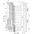
図1は実施の形態1に係る半導体装置として、SJ構造を有する炭化珪素半導体装置100のピラー部の構成を模式的に示す斜視図である。炭化珪素半導体装置100は、半導体基板の主面に対して垂直な方向に主電流が流れる縦型MOSFETを示しているが、便宜的に、主電極およびMOSFETのユニットセルなどは図示を省略している。<
<Device configuration>
FIG. 1 is a perspective view schematically showing a configuration of a pillar portion of a silicon
ピラー部7は、図1に示されるように、平面視形状がストライプ状の複数のn型ピラー7n(第1のピラー)と、複数のp型ピラー7p(第2のピラー)とが、それぞれの長手方向に直交する幅方向において並列するように半導体基板3上に交互に配列された領域である。これらの配列方向は、炭化珪素半導体装置100の主電流が流れる方向に直交する方向である。ピラー部7を囲むようにp型不純物を含むp型ピラー周辺部6が設けられており、p型ピラー周辺部6のさらに外側はp型不純物を含むp型チップ周辺部5となっている。
As shown in FIG. 1, the
半導体基板3は、n+型のSiC基板であり、例えば市販されている4H-SiCのn型基板であって、[11-20]方向に4度のオフ角を有し、300~400μmの厚みを有し、n型不純物の濃度は5×10¹⁸~1×1020cm-3である。The
半導体基板3とp型チップ周辺部5との間にはn型不純物を含むn型SiC層4(第1の半導体層)が設けられており、その厚さは0.5~10μm、n型不純物の濃度は1×10¹⁴~5×1019cm-3である。なお、半導体基板3とn型SiC層4とを合わせて半導体基体と呼称する場合がある。An n-type SiC layer 4 (first semiconductor layer) containing n-type impurities is provided between the
図1におけるA-A線(Y軸に並行な線)での矢示方向の断面図を図2に示し、B-B線(X軸に並行な線)での矢示方向の断面図を図3に示す。図2および図3に示されるようにn型ピラー7nおよびp型ピラー7pは、n型SiC層4上から高さ方向(Z軸方向)突出するように設けられ、p型ピラー周辺部6がピラー部7を囲み、p型チップ周辺部5がn型SiC層4の外周上を覆っている。なお、n型SiC層4の端面は、半導体チップの側面に露出している。
FIG. 2 shows a cross-sectional view in the direction of the arrows along line AA (a line parallel to the Y axis) in FIG. 1, and a cross-sectional view in the direction of the arrows along line BB (a line parallel to the X axis) It is shown in FIG. As shown in FIGS. 2 and 3, the n-
図4は、n型ピラー7nおよびp型ピラー7pの大きさを示す図であり、n型ピラー7nのピラー幅7nWと、p型ピラー7pのピラー幅7pWとは同等であり、例えば、0.5~5μmの長さに形成される。また、n型ピラー7nのピラー高さ7nHと、p型ピラー7pのピラー幅7pHとは同等であり、例えば、5~100μmの高さに形成される。そして、n型ピラー7nの不純物濃度と幅の積が、p型ピラー7pの不純物濃度と幅の積にほぼ一致するように形成され、n型不純物およびp型不純物の濃度は、それぞれ例えば5×10¹⁵~1×1018cm-3である。このような構成とすることで、炭化珪素半導体装置100がオフの状態では、n型ピラー7nおよびp型ピラー7pの全体に空乏層が広がる。FIG. 4 is a diagram showing the sizes of the n-
p型ピラー7pとの接合部での電界を緩和するためには、n型SiC層4の不純物濃度は、n型ピラー7nの不純物濃度と同じか低い方が良いが、n型ピラー7nの不純物濃度よりも高濃度とすることもできる。また、n型SiC層4を設けず、n型ピラー7nおよびp型ピラー7pが半導体基板3に直接接合することもできる。n型SiC層4の不純物濃度が、n型ピラー7nの不純物濃度よりも高濃度である場合、また、n型SiC層4を設けない場合は、n型SiC層4の不純物濃度が、n型ピラー7nの不純物濃度と同じか低い場合に比べると効果は小さくなるが、図1に示されるようなピラー部7を設けることで、従来の構造と比べて高耐圧で低抵抗な炭化珪素半導体装置を実現できる。
In order to relax the electric field at the junction with the p-
なお、図1~図4では、ピラー部7にp型ピラー7pを3個、n型ピラー7nを4個設けた構成を示したが、実際には炭化半導体装置の大きさに応じた数のp型ピラー7pおよびn型ピラー7nが形成される。先に説明したように、ピラー幅は0.5~5μmであり、MOSFETのユニットセルが設けられるMOSFETセル領域の全体のY方向の幅は、例えば1~10mmであるので、少なくともMOSFETセル領域に収まる個数のp型ピラー7pおよびn型ピラー7nが形成される。
1 to 4 show a configuration in which three p-
また、図3および図4に示されるように、p型ピラー周辺部6の幅6Wをp型ピラー7pの幅7pWよりも厚くすることで、p型ピラー周辺部6とp型ピラー7pとで不純物濃度が同じ場合、p型ピラー周辺部6の不純物濃度と幅の積が、p型ピラー7pの不純物濃度と幅の積よりも大きくなる。このような構成とすることで、p型ピラー周辺部6の全体に空乏層が広がらず、p型ピラー周辺部6の電界強度が低く抑えられ、リーク電流増加および放電リスクが抑制される。この場合、p型ピラー周辺部6の幅は、p型ピラー7pの幅の1.2倍以上とすることができる。
Further, as shown in FIGS. 3 and 4, by making the
また、p型ピラー周辺部6の幅6Wとp型ピラー7pの幅7pWとが同じ場合でも、p型ピラー周辺部6の不純物濃度をp型ピラー7pの不純物濃度の1.2倍以上とすることで、p型ピラー周辺部6の全体に空乏層が広がらず、p型ピラー周辺部6の電界強度が低く抑えられ、リーク電流増加および放電リスクが抑制される。
Further, even when the
図5は、ピラー部7にMOSFETのユニットセルを設けた場合のMOSFETセル領域MCRと、その外周に設けられるMOSFET終端領域MTRとを模式的に示す炭化珪素半導体装置100の斜視図である。
FIG. 5 is a perspective view of a silicon
MOSFETセル領域MCRの構成について、図6および図7を用いて説明する。図6は図5におけるC-C線(Y軸に並行な線)での矢示方向の断面図であり、図6における領域Aの拡大図を図7に示す。 The configuration of MOSFET cell region MCR will be described with reference to FIGS. 6 and 7. FIG. 6 is a cross-sectional view taken along line CC (a line parallel to the Y-axis) in FIG. 5, and an enlarged view of area A in FIG. 6 is shown in FIG.
図7に示すようにMOSFETは、半導体基板3の一方の主面上にn型SiC層4が設けられ、n型SiC層4上には、複数のp型ピラー7pおよび複数のn型ピラー7nが交互に設けられている。そして、p型ピラー7pの上層部から、n型ピラー7nの上層部にかけて、p型のウェル領域8が選択的に複数設けられ、それぞれのウェル領域8にはp型のコンタクト領域10が、ウェル領域8を貫通するように設けられている。
As shown in FIG. 7, the MOSFET has an n-
そして、ウェル領域8の上層部にはコンタクト領域10の両側面に接してn型のソース領域9が設けられている。なお、ソース領域9の厚みは、ウェル領域8の厚みより薄く、コンタクト領域10の厚みはウェル領域8の厚みと同程度か、あるいはコンタクト領域10の方が少し深くなるように設けられ、p型ピラー7pに電気的に接続されるように構成されている。
An n-
隣り合うウェル領域8のソース領域9上に跨がるようにゲート絶縁膜11が選択的に形成され、ゲート絶縁膜11上にはゲート電極12が形成されている。すなわち、ゲート絶縁膜11は、隣り合うソース領域9間において、ソース領域9の一部上部からウェル領域8上およびn型ピラー7n上から、隣り合うウェル領域8のソース領域9の一部上部に渡るように設けられ、ゲート絶縁膜11上にゲート電極12が設けられている。
A
そして、ゲート絶縁膜11およびゲート電極12を覆うように層間絶縁膜13が形成され、層間絶縁膜13を覆うようにソース電極14が形成されている。層間絶縁膜13には、ゲート電極12を覆う領域以外の領域で、層間絶縁膜13を厚さ方向に貫通してソース領域9の一部およびコンタクト領域10の全部の表面に達するコンタクトホールが設けられている。そして、コンタクトホール内にはソース電極14が充填され、ソース電極14がソース領域9およびコンタクト領域10に接続されている。
また、ソース電極14が設けられた側とは反対側の半導体基板3の他方の主面(裏面)上にはドレイン電極15が設けられている。なお、MOSFETセル領域MCRおよびMOSFET終端領域MTRの構成の一例については、後にさらに説明する。
A
以上説明したように、半導体基板3上に、平面視形状がストライプ状の複数のn型ピラー7nと、複数のp型ピラー7pとを交互に配列したピラー部7を設けることで、p型ピラー7pをエピタキシャル成長で形成する際にボイドが形成されず、無効領域を低減することができる。このため、ボイドを切り離すための加工が不要になり、製造コストを低減できる。
As described above, on the
また、図7においては、MOSFETのユニットセルを2個設けた構成を示したが、実際には炭化半導体装置の大きさに応じた数のユニットセルが形成される。 Also, although FIG. 7 shows a configuration in which two MOSFET unit cells are provided, in practice, the number of unit cells is formed according to the size of the carbide semiconductor device.
<変形例1>
図8は、実施の形態1の変形例1の炭化珪素半導体装置100Aの構成を示す断面図であり、図7に対応する断面図である。図8に示されるように、炭化珪素半導体装置100Aは、n型SiC層4を設ける代わりに、ウェル領域8間にn型SiC層40(第2のn型SiC層)が設けられている。<
FIG. 8 is a cross-sectional view showing a configuration of silicon
<変形例2>
図9は、実施の形態1の変形例2の炭化珪素半導体装置100Bの構成を示す断面図であり、図2に対応する断面図である。図9に示されるように、炭化珪素半導体装置100Bは、n型SiC層4上にp型チップ周辺部5が設けられていない構成を有している。<Modification 2>
FIG. 9 is a cross-sectional view showing a configuration of silicon
このような構成は、p型ピラー7pを埋め込みエピ法により形成する場合に、全面エッチングによりp型ピラー7pを形成する場合に作りやすいという特徴を持つ。また図9では、n型SiC層4は均一な厚さになっているが、p型チップ周辺部5を除去した領域のn型SiC層4の厚さが、p型ピラー周辺部6およびp型ピラー7pの下部の厚さより、小さくすることもできる。
Such a structure is characterized in that it is easy to fabricate when the p-
<変形例3>
図10および図11は、実施の形態1の変形例3の炭化珪素半導体装置100Cの構成を示す断面図であり、それぞれ図2および図3に対応する断面図である。図10および図11に示されるように、炭化珪素半導体装置100Bはn型SiC層4のピラー周辺部高さ4H2が、ピラー部7でのn型SiC層4の高さ4H1より低くなっている。<
10 and 11 are cross-sectional views showing a configuration of silicon carbide semiconductor device 100C of
図12は、このような構成を採った場合のMOSFETセル領域MCRにおける主電流の流れを矢印で模式的に示した図である。図12に示されるようにMOSFETセル領域MCRにおける主電流は、MOSFETセル領域MCRに流れ、チップ周辺部に電流が流れにくくなっている。これは、n型SiC層4のピラー周辺部の厚みが薄くなることで電流経路が狭くなり、チップ周辺部への主電流の広がり幅が狭くなって、チップ周辺部に広がるよりも先に主電流が半導体基板3に到達するためである。なお、高さ4H1と高さ4H2の比率は、例えば2対1程度とすることができる。
FIG. 12 is a diagram schematically showing, by arrows, the flow of the main current in the MOSFET cell region MCR when such a configuration is adopted. As shown in FIG. 12, the main current in the MOSFET cell region MCR flows through the MOSFET cell region MCR, making it difficult for the current to flow through the chip periphery. This is because the thickness of the pillar periphery of the n-
チップ周辺部はダイシング時の欠陥などがあり、主電流が流れると不具合が生じやすい。n型SiC層4のピラー周辺部高さ4H2を、ピラー部7でのn型SiC層4のピラー高さ4H1より低くすることでチップ周辺部に主電流が流れにくくなり、MOSFETに主電流として大電流が流れた場合の電流耐量が大きくなる。
The chip periphery has defects during dicing, and problems are likely to occur when the main current flows. By making the pillar peripheral portion height 4H2 of the n-
半導体として炭化硅素を用いた炭化珪素半導体装置は、半導体として硅素を用いた半導体装置と比較して、耐圧性に優れ、許容電流密度も高く、耐熱性に優れ高温動作可能な半導体装置を得ることができる。 A silicon carbide semiconductor device using silicon carbide as a semiconductor has excellent withstand voltage, high allowable current density, excellent heat resistance and high temperature operation as compared with a semiconductor device using silicon as a semiconductor. can be done.
<実施の形態2>
<ピラー部の製造方法>
次に、実施の形態2として、炭化珪素半導体装置200のピラー部の製造方法について説明する。まず、図13に示す工程において、例えば市販されている4H-SiCのn型基板であって、[11-20]方向に4度のオフ角を有し、300~400μmの厚みを有し、n型不純物の濃度が5×10¹⁸~1×1020cm-3である半導体基板3を準備する。<Embodiment 2>
<Manufacturing Method of Pillar Part>
Next, a method for manufacturing a pillar portion of silicon
次に、図14に示す工程において、半導体基板3の一方の主面上に、エピタキシャル成長によりn型不純物を含むn型SiC層70(第1の半導体層)を形成する。n型SiC層70は、例えば厚さ5~100μm、不純物濃度はn型不純物の濃度は1×10¹⁵~1×1018cm-3とすることができる。なお、半導体基板3とn型SiC層70とを合わせて半導体基体と呼称する場合がある。14, an n-type SiC layer 70 (first semiconductor layer) containing n-type impurities is formed on one main surface of the
次に、図15に示す工程において、ドライエッチングによりn型SiC層70をエッチングして、n型SiC層70の凸部72と、n型SiC層70のn型チップ周辺部71を形成する。半導体基板3が[11-20]方向に4度のオフ角を有している場合は、凸部72は平面視形状が、X軸([11-20]方向)に平行な方向に延在するストライプ状をなし、Y軸([1-100]方向)に沿った方向に間隔を開けて複数の凸部72が配列されるように形成される。n型SiC層70は、[11-20]方向に垂直な方向には対称な形状になるため、エピタキシャル成長で凸部72間にp型SiC層を形成する際に、p型SiC層の形状を制御しやすくなる。なお、凸部72は、Y軸方向の幅が例えば0.5~5μm、Z軸([0001]方向)方向の高さが例えば5~100μmの範囲で形成される。
Next, in the process shown in FIG. 15, the n-
一方、半導体基板3にオフ角のない基板を用いた場合は、ストライプ状の凸部72は、[11-20]方向から[0001]軸の周りに90度回転した方位に形成することができる。つまり、図15における[11-20]軸と[1-100]軸を入れ替えた方位に凸部72を形成しても、エピタキシャル成長で凸部72間に形成されるp型SiC層は対称な形状になるため、p型SiC層の形状を制御しやすくなる。
On the other hand, when a substrate having no off-angle is used as the
次に、図16に示す工程において、エピタキシャル成長によりn型SiC層70のn型チップ周辺部71および凸部72を覆うようにp型SiC層60(第2の半導体層)を形成する。図16では、n型SiC層70の凸部72のp型SiC層60の表面は平坦になっているが、凹凸を有していても良い。
Next, in the step shown in FIG. 16, the p-type SiC layer 60 (second semiconductor layer) is formed by epitaxial growth so as to cover the n-type chip
図15に示したように、n型SiC層70の凸部72の周囲が、n型チップ周辺部71として掘り下げられた状態でp型SiC層60をエピタキシャル成長させることで、結晶面方位の違いに起因する結晶成長速度の差によるボイドが形成がされず、無効領域を低減することができる。このため、ボイドを切り離すための加工が不要になり、製造コストを低減できる。
As shown in FIG. 15, by epitaxially growing the p-
p型SiC層60のp型不純物の濃度は、n型ピラー7nの不純物濃度と幅の積が、p型ピラー7pの不純物濃度と幅の積にほぼ一致するように設定すると良い。
The p-type impurity concentration of the p-
次に、図17に示す工程において、研磨あるいはドライエッチングによりn型SiC層70の凸部72上のp型SiC層60を除去して、凸部72の上面を露出させると共に、凸部72間にp型SiC層60を残す。凸部72がn型ピラー7nとなり凸部72間のp型SiC層60がp型ピラー7pとなってピラー部7を構成する。また、ピラー部7を囲むように所定の幅を有するp型ピラー周辺部6が形成される。なお、n型SiC層70の凸部72の上部を一部除去することができる。また、n型SiC層70のn型チップ周辺部71上のp型チップ周辺部5の上部を一部除去することができる。
17, the p-
以上の方法により形成された炭化珪素半導体装置200のMOSFETセル領域MCRおよびMOSFET終端領域MTRが形成される前の斜視図を図18に示す。図18に示されるように、炭化珪素半導体装置200においては、n型SiC層70のn型チップ周辺部71の端面が半導体チップの側面に露出していることを除いて、図1に示した炭化珪素半導体装置100と同じである。
FIG. 18 shows a perspective view of silicon
なお、図14~図18では、ピラー部7にp型ピラー7pを3個、n型ピラー7nを4個設けた構成を示したが、実際には炭化半導体装置の大きさに応じた数のp型ピラー7pおよびn型ピラー7nが形成される。
14 to 18 show a configuration in which three p-
次に、図18おけるA-A線(Y軸に並行な線)での矢示方向の断面図およびB-B線(X軸に並行な線)での矢示方向の断面図を用いて炭化珪素半導体装置200のピラー部の製造方法の変形例について説明する。
Next, using a cross-sectional view in the direction of the arrows along line AA (a line parallel to the Y axis) and a cross-sectional view in the direction of the arrows along line BB (a line parallel to the X axis) in FIG. A modification of the method for manufacturing the pillar portion of silicon
まず、図14~図17に示した工程でのA-A線およびB-B線での断面図を図19~図25に示す。図19は図14に示した工程でのA-A線での断面図である。なお、B-B線での断面図は図19と同じである。図20は図15に示した工程でのA-A線での断面図であり、図21はB-B線での断面図である。図22は図16に示した工程でのA-A線での断面図であり、図23はB-B線での断面図である。図24は図17に示した工程でのA-A線での断面図であり、図25はB-B線での断面図である。 First, FIGS. 19 to 25 are sectional views taken along the lines AA and BB in the steps shown in FIGS. 14 to 17. FIGS. FIG. 19 is a cross-sectional view along line AA in the process shown in FIG. Note that the cross-sectional view taken along line BB is the same as FIG. 20 is a cross-sectional view taken along line AA in the process shown in FIG. 15, and FIG. 21 is a cross-sectional view taken along line BB. 22 is a cross-sectional view taken along line AA in the process shown in FIG. 16, and FIG. 23 is a cross-sectional view taken along line BB. 24 is a cross-sectional view taken along line AA in the process shown in FIG. 17, and FIG. 25 is a cross-sectional view taken along line BB.
<ピラー部の製造方法の変形例1>
図19に示した構成に対して、図26に示されるように、半導体基板3の一方の主面上にエピタキシャル成長によりn型不純物を含むn型SiC層4を形成し、さらにその上にエピタキシャル成長によりn型不純物を含むn型SiC層70を形成して2層構造とすることができる。この場合、1層目となるn型SiC層4は、例えば厚さ0.5~10μm、n型不純物の濃度を1×10¹⁴~1×1019cm-3とし、2層目となるn型SiC層70は、例えば厚さ5~100μm、n型不純物の濃度を1×10¹⁵~1×1018cm-3とすることができる。なお、n型SiC層4およびn型SiC層70は、共に第1のn型SiC層と呼称することができる。<Modified Example 1 of Manufacturing Method of Pillar Portion>
For the structure shown in FIG. 19, as shown in FIG. 26, an n-
このように第1のn型SiC層を2層構造とすることで、半導体基板3とエピタキシャル層との間で、不純物濃度の差に起因する結晶の格子定数の違いによるひずみを緩和することができる。なお、1層目と2層目とで厚さおよび不純物濃度を変えるのは、1層目と2層目とでひずみを緩和させるために必要な厚さおよび不純物濃度が異なるためである。
By forming the first n-type SiC layer into a two-layer structure in this way, it is possible to relax the distortion caused by the difference in crystal lattice constant caused by the difference in impurity concentration between the
第1のn型SiC層を2層構造とした場合、図20に示した構成に対して、図27に示されるように第1のn型SiC層の周辺部をn型SiC層4の1層だけとすることもでき、1層だけとなったn型SiC層4の厚みを薄くすることもできる。このように、チップ周辺部の第1のn型SiC層の厚さを薄くすることで、図12を用いて説明したように、MOSFETの主電流がチップ周辺部に流れにくくなり、MOSFETに主電流として大電流が流れた場合の電流耐量が大きくなる。
When the first n-type SiC layer has a two-layer structure, as shown in FIG. It is also possible to reduce the thickness of the n-
また、図28に示されるように第1のn型SiCの周辺部に2層目のn型SiC層70を一部残すこともできる。このような構成とすることで、ピラーの底部が同じ不純物濃度のエピタキシャル層に接触するため、接触部分での電界バランスを保つ設計が容易となり、耐圧を保持しやすくなる。
Also, as shown in FIG. 28, a part of the second n-
<ピラー部の製造方法の変形例2>
図19に示した構成のように、第1のn型SiC層を単層構造とした場合は、図29に示すように、ドライエッチングによりn型SiC層70をエッチングする際にして、オーバエッチングにより半導体基板3を部分的に除去し、半導体基板3に凹凸を形成することができる。このような構成とすることで、ピラーの底部が高不純物濃度の半導体基板3と接触するので、抵抗を低減することができる。<Modified Example 2 of Manufacturing Method of Pillar Portion>
When the first n-type SiC layer has a single-layer structure as in the configuration shown in FIG. 19, as shown in FIG. can partially remove the
また、図30に示すように、ドライエッチングによりn型SiC層70をエッチングする際にして、オーバエッチングが発生しないようにエッチングを行うことで、凸部72の下に第1のn型SiC、すなわちn型SiC層70が残らない構成とすることができる。このような構成とすることで、ピラーの底部が高不純物濃度の半導体基板3と接触するので、抵抗を低減することができ、また、図29に示した構成と比較して、電界バランスを保つ設計が容易となる。
Further, as shown in FIG. 30, when the n-
<半導体装置の製造方法>
図31は、ピラー部7にMOSFETのユニットセルを設けた場合のMOSFETセル領域MCRと、その外周に設けられるMOSFET終端領域MTRとを模式的に示す炭化珪素半導体装置200の斜視図である。<Method for manufacturing a semiconductor device>
FIG. 31 is a perspective view of a silicon
MOSFETセル領域MCRにおけるMOSFETセルの製造工程について、図32~図35を用いて説明する。図32は図24に対応する断面図であり、図32における領域Bの拡大図を図33に示す。なお、図33においては、図7を用いて説明した構成と同一の構成については同一の符号を付し、重複する説明は省略する。 A manufacturing process of the MOSFET cell in the MOSFET cell region MCR will be described with reference to FIGS. 32 to 35. FIG. FIG. 32 is a sectional view corresponding to FIG. 24, and FIG. 33 shows an enlarged view of region B in FIG. In addition, in FIG. 33, the same reference numerals are assigned to the same configurations as those described using FIG. 7, and overlapping descriptions are omitted.
図33に示すように、半導体基板3の一方の主面上にn型SiC層70が設けられ、n型SiC層70上には、複数のp型ピラー7pおよび複数のn型ピラー7nが交互に設けられている。そして、p型ピラー7pの上層部から、n型ピラー7nの上層部にかけて、p型不純物のイオン注入によりp型のウェル領域8を選択的に複数形成する。また、それぞれのウェル領域8には、ウェル領域8を貫通するようにp型不純物のイオン注入によりp型のコンタクト領域10を形成する。また、ウェル領域8の上層部にはコンタクト領域10の両側面に接するようにn型不純物のイオン注入によりn型のソース領域9を形成する。イオン注入により形成された結晶欠陥を回復するため活性化アニールを行い、注入された不純物を活性化させる。
As shown in FIG. 33, an n-
なお、p型のウェル領域8の厚さは、例えば0.2~1.5μm、p型不純物の濃度は、例えば1×10¹⁴~1×1019cm-3とし、ソース領域9の厚さは、例えば0.1~0.5μm、n型不純物の濃度は、例えば1×10¹⁷~1×1021cm-3とし、コンタクト領域10の厚さは、例えば0.2~1.5μm、p型不純物の濃度は、例えば1×10¹⁸~1×10²¹m-3とすることができる。なお、図面ではウェル領域8およびコンタクト領域10の厚さは同じに描かれているが、両者が同じ厚さに限定されるものではない。The thickness of the p-
その後、図34に示す工程において、ピラー部7上に、ゲート絶縁膜11の材料となる絶縁膜、例えばシリコン酸化膜111を形成し、さらに、シリコン酸化膜111上にゲート電極12となる導体膜、例えばポリシリコン膜を形成する。そして、ポリシリコン膜をパターニングして隣り合うソース領域9の端縁部上方に跨がるようにゲート電極12を形成する。その後、ゲート電極12およびシリコン酸化膜111を覆うように、層間絶縁膜13の材料となる絶縁膜、例えばシリコン酸化膜131を形成する。
34, an insulating film, for example, a
その後、図35に示す工程において、シリコン酸化膜111および131をパターニングして、ゲート絶縁膜11およびゲート電極12を覆う層間絶縁膜13を形成する。このパターニングでは、層間絶縁膜13を厚さ方向に貫通してソース領域9の一部およびコンタクト領域10の全部の表面に達するコンタクトホールが形成される。その後、コンタクトホール内を埋め込むと共に層間絶縁膜13上を覆うように導体膜を形成してソース電極14を形成し、また、ソース電極14が設けられた側とは反対側の半導体基板3の他方の主面(裏面)上にドレイン電極15を形成することで、炭化珪素半導体装置200が完成する。なお、MOSFETセル領域MCRおよびMOSFET終端領域MTRの製造方法の一例については、後にさらに説明する。
Thereafter, in the step shown in FIG. 35,
図35に示した炭化珪素半導体装置200においては、p型ピラー7pの上層部から、n型ピラー7nの上層部にかけてp型のウェル領域8を選択的に複数設け、また、それぞれのウェル領域8に、p型のコンタクト領域10およびn型のソース領域9を設けた構成を示したが、n型ピラー7nおよびp型ピラー7pの上層部にp型のウェル領域8等を設けるのではなく、n型ピラー7nおよびp型ピラー7pの上にn型SiC層40(第3の半導体層)を設けて、n型SiC層40内にp型のウェル領域8等を設けた構成とすることができる。以下、その製造工程について、半導体装置の製造方法の他の例として図36~図40を用いて説明する。
In silicon
図17を用いて説明した工程の後、図36に示す工程において、ピラー部7上からp型チップ周辺部5上にかけての領域を覆うようにエピタキシャル成長によりn型SiC層40を形成する。n型SiC層40は、半導体チップ全面に形成することもでき、MOSFETセルを形成するMOSFETセル領域だけ形成することもでき、また、MOSFETセル領域とMOSFET終端領域に形成することもできる。
After the step described with reference to FIG. 17, in the step shown in FIG. 36, an n-
図37は図36の拡大領域を示す図面であり、図37における領域Cの拡大図を図38に示す。なお、図38においては、図7を用いて説明した構成と同一の構成については同一の符号を付し、重複する説明は省略する。 37 is a drawing showing an enlarged area of FIG. 36, and an enlarged view of area C in FIG. 37 is shown in FIG. In addition, in FIG. 38, the same reference numerals are assigned to the same configurations as those described using FIG. 7, and duplicate descriptions will be omitted.
図38に示すように、p型ピラー7pの上方からn型ピラー7nの上方にかけてのn型SiC層40内に、p型不純物のイオン注入によりp型のウェル領域8を選択的に複数形成する。また、それぞれのウェル領域8には、ウェル領域8を貫通するようにp型不純物のイオン注入によりp型のコンタクト領域10を形成する。また、ウェル領域8の上層部にはコンタクト領域10の両側面に接するようにn型不純物のイオン注入によりn型のソース領域9を形成する。イオン注入により形成された結晶欠陥を回復するため活性化アニールを行い、注入された不純物を活性化させる。
As shown in FIG. 38, a plurality of p-
その後、図39に示す工程において、n型SiC層40上に、ゲート絶縁膜11の材料となる絶縁膜、例えばシリコン酸化膜111を形成し、さらに、シリコン酸化膜111上にゲート電極12となる導体膜、例えばポリシリコン膜を形成する。そして、ポリシリコン膜をパターニングして隣り合うソース領域9の端縁部上方に跨がるようにゲート電極12を形成する。その後、ゲート電極12およびシリコン酸化膜111を覆うように、層間絶縁膜13の材料となる絶縁膜、例えばシリコン酸化膜131を形成する。
After that, in the process shown in FIG. 39, an insulating film, for example, a
その後、図40に示す工程において、シリコン酸化膜111および131をパターニングして、ゲート絶縁膜11およびゲート電極12を覆う層間絶縁膜13を形成する。このパターニングでは、層間絶縁膜13を厚さ方向に貫通してソース領域9の一部およびコンタクト領域10の全部の表面に達するコンタクトホールが形成される。その後、コンタクトホール内を埋め込むと共に層間絶縁膜13上を覆うように導体膜を形成してソース電極14を形成し、また、ソース電極14が設けられた側とは反対側の半導体基板3の他方の主面(裏面)上にドレイン電極15を形成することで、炭化珪素半導体装置200Aが完成する。
Thereafter, in the step shown in FIG. 40,
なお、図40に示した炭化珪素半導体装置200Aでは、p型のウェル領域8の厚さとn型SiC層40の厚さを同等としたが、図41に示すようにp型のウェル領域8をn型SiC層40の厚さよりも深くまで形成することができる。このような構成とすることで、高濃度のn型SiC層40にp型のウェル領域8の角部が接触せず、MOSFETへの高電圧印加時にp型のウェル領域8の角部の電界強度を低減して耐圧を保持することができる。なお、p型のウェル領域8の深さは、n型SiC層40の厚さ0.1~1μm程度深くする。
In silicon
以上説明した実施の形態2の炭化珪素半導体装置200および200Aにおいても、p型ピラー7pをエピタキシャル成長で形成する際にボイドが形成されず、無効領域を低減することができる。このため、ボイドを切り離すための加工が不要になり、製造コストを低減できる。
In silicon
また、図35および図40においては、MOSFETのユニットセルを2個設けた構成を示したが、実際には炭化半導体装置の大きさに応じた数のユニットセルが形成される。 35 and 40 show a configuration in which two MOSFET unit cells are provided, actually, the number of unit cells is formed according to the size of the carbide semiconductor device.
<半導体装置の製造方法の変形例1>
図42および図43を用いて、実施の形態2の炭化珪素半導体装置の製造方法の変形例1について説明する。なお、図42および図43は、それぞれ図22および図23に対応する図である。<
図15および図20を用いて説明したように、n型SiC層70の凸部72と、n型SiC層70のn型チップ周辺部71を形成した後、エピタキシャル成長によりn型SiC層70のn型チップ周辺部71および凸部72を覆うようにp型SiC層60を形成する際に、図42および図43に示すように、p型SiC層60をn型SiC層70の凸部72間が埋め込まれた後もエピタキシャル成長を継続することで、p型ピラー周辺部6の幅6Wをp型ピラー7pの幅7pWより大幅に大きく形成する。
As described with reference to FIGS. 15 and 20, after forming the
この結果、p型ピラー周辺部6とp型ピラー7pとで不純物濃度が同じ場合、p型ピラー周辺部6の不純物濃度と幅の積が、p型ピラー7pの不純物濃度と幅の積よりも大幅に大きくなる。このような構成とすることで、p型ピラー周辺部6の全体に空乏層が広がらず、p型ピラー周辺部6の電界強度が低く抑えられ、リーク電流増加および放電リスクが抑制される。
As a result, when the impurity concentration is the same in the p-type pillar
<半導体装置の製造方法の変形例2>
図44および図45を用いて、実施の形態2の炭化珪素半導体装置の製造方法の変形例2について説明する。なお、図44および図45は、それぞれ図22および図23に対応する図である。<Modification 2 of Method for Manufacturing Semiconductor Device>
Modification 2 of the method for manufacturing the silicon carbide semiconductor device of Embodiment 2 will be described with reference to FIGS. 44 and 45 . 44 and 45 are diagrams corresponding to FIGS. 22 and 23, respectively.
図15および図20を用いて説明したように、n型SiC層70の凸部72と、n型SiC層70のn型チップ周辺部71を形成した後、エピタキシャル成長によりn型SiC層70のn型チップ周辺部71および凸部72を覆うようにp型SiC層60を形成する際に、図44および図45に示すように、p型ピラー周辺部6のp型の不純物濃度が、p型ピラー7pのp型の不純物濃度より高くなるように形成する。このためには、p型SiC層60のエピタキシャル条件を調整して、n型SiC層70の凸部72間よりもp型ピラー周辺部6の方がp型不純物を取り込みやすくする。
As described with reference to FIGS. 15 and 20, after forming the
すなわち、エピタキシャル成長時の原料ガス比、温度、圧力を調整することで、結晶面による不純物の取り込み量が変わる。p型ピラー周辺部6はトレンチ底面からの結晶成長にほぼ限られるが、凸部72間ではトレンチ底面とトレンチ側壁の複数の面から結晶成長するため、不純物の取り込み量が異なる。また、広い面積で掘り下げられたp型ピラー周辺部6と、狭い幅で掘り下げられた凸部72間とでは原料ガスおよび不純物ガスの供給されやすさが異なることも影響するので、これらの要素を考慮してp型SiC層60のエピタキシャル条件を調整する。
That is, by adjusting the material gas ratio, temperature, and pressure during epitaxial growth, the amount of impurities taken in by the crystal face changes. The p-type pillar
この結果、p型ピラー周辺部6の幅6Wとp型ピラー7pの幅7pWとが同じ場合でも、p型ピラー周辺部6の不純物濃度と幅の積が、p型ピラー7pの不純物濃度と幅の積よりも大きくなる。このような構成とすることで、p型ピラー周辺部6の全体に空乏層が広がらず、p型ピラー周辺部6の電界強度が低く抑えられ、リーク電流増加および放電リスクが抑制される。
As a result, even when the
また、p型SiC層60を図42~図45の構成を組み合わせて形成することで、p型ピラー周辺部6の不純物濃度と幅の積が、p型ピラー7pの不純物濃度と幅の積よりも大幅に大きくなるようにすることができる。このような構成とすることで、p型ピラー周辺部6の全体に空乏層が広がらず、p型ピラー周辺部6の電界強度が低く抑えられ、リーク電流増加および放電リスクが抑制される。
Further, by forming the p-
<半導体装置の製造方法の変形例3>
図46および図47を用いて、実施の形態2の炭化珪素半導体装置の製造方法の変形例3について説明する。なお、図46および図47は、それぞれ図22および図23に対応する図である。<
図15および図20を用いて説明したように、n型SiC層70の凸部72と、n型SiC層70のn型チップ周辺部71を形成した後、エピタキシャル成長によりn型SiC層70のn型チップ周辺部71および凸部72を覆うようにp型SiC層60を形成した後、図46および図47に示すように、p型ピラー周辺部6にp型不純物のイオン注入を行い、p型ピラー周辺部6のp型不純物の濃度が、p型ピラー7pのp型の不純物濃度より高くなるようにする。
As described with reference to FIGS. 15 and 20, after forming the
この結果、p型ピラー周辺部6の不純物濃度と幅の積が、p型ピラー7pの不純物濃度と幅の積よりも大きくなる。このような構成とすることで、p型ピラー周辺部6の全体に空乏層が広がらず、p型ピラー周辺部6の電界強度が低く抑えられ、リーク電流増加および放電リスクが抑制される。
As a result, the product of the impurity concentration and the width of the p-type pillar
なお、p型ピラー周辺部6へのイオン注入は必要な箇所のみ実施することができる。SiCの場合、結晶方位によってエピタキシャル成長速度およびエピタキシャル濃度が異なる場合がある。この結果、p型SiC層60をエピタキシャル成長した際に、p型ピラー周辺部6の不純物濃度と幅の積が均一に形成されない場合があり、p型ピラー周辺部6の不純物濃度と幅の積が、p型ピラー7pの不純物濃度と幅の積よりも小さい場所が形成されることがある。その場合はp型ピラー周辺部6の濃度と幅の積がp型ピラー周辺部6の不純物濃度と幅の積より小さい部分にのみイオン注入を行い、p型ピラー周辺部6の濃度と幅の積がp型ピラー周辺部6の不純物濃度と幅の積より大きくすることができる。
It should be noted that the ion implantation into the p-type pillar
なお、同じ構造、大きさの半導体装置であれば、p型ピラー周辺部6の不純物濃度と幅の積が、p型ピラー7pの不純物濃度と幅の積よりも小さい場所はいつも同じ場所に発生するので、サンプルを作り分解、検証することで特定することができる。
If the semiconductor device has the same structure and size, the place where the product of the impurity concentration and the width of the p-type pillar
また、p型ピラー周辺部6の不純物濃度と幅の積が、p型ピラー7pの不純物濃度と幅の積よりも小さくなる原因としては、エピタキシャル条件によって、p型ピラー周辺部6の幅が狭くなったり、結晶面によるp型不純物の取り込み量が少なく、p型不純物の濃度が低くなったりすることが考えられる。
The reason why the product of the impurity concentration and the width of the p-type pillar
<半導体装置の製造方法の変形例4>
図48を用いて、実施の形態2の炭化珪素半導体装置の製造方法の変形例4について説明する。なお、図48は図24に対応する図である。<
図17および図24を用いて説明したように、研磨あるいはドライエッチングによりn型SiC層70の凸部72上のp型SiC層60を除去して、凸部72の上面を露出させる際に、図48に示されるように、p型ピラー周辺部6の外側のp型チップ周辺部5を除去する。
As described with reference to FIGS. 17 and 24, when the p-
このような構成とすることで、全面エッチングによりp型SiC層60の凸部72上のp型SiC層60と同時にp型チップ周辺部5を除去することができ、製造工程を簡略化できる。この際、n型SiC層70のn型チップ周辺部71の一部を除去することもできる。
With such a structure, the p-
<半導体装置の製造方法の変形例5>
図49および図50を用いて、実施の形態2の炭化珪素半導体装置の製造方法の変形例5について説明する。なお、図49および図50は、それぞれ図20および図21に対応する図である。<
図27を用いて説明したように、第1のn型SiC層の周辺部をn型SiC層4の1層だけとした場合、1層だけとなったn型SiC層4の厚みを薄くすることもできる。この結果、n型SiC層4のピラー周辺部高さ4H2が、ピラー部7でのn型SiC層4の高さ4H1より低くなる。このように、チップ周辺部の第1のn型SiC層の厚さを薄くすることで、図12を用いて説明したように、MOSFETの主電流がチップ周辺部に流れにくくなり、MOSFETに主電流として大電流が流れた場合の電流耐量が大きくなる。
As described with reference to FIG. 27, when only one layer of the n-
<ダイシング工程>
図51および図52を用いて、ウエハプロセスを経て製造された半導体装置をチップ単位に分離するダイシング工程を説明する。図51および図52は、ウエハ状態で隣り合う炭化珪素半導体装置200を示した断面図に相当し、図51は図18のA-A線での矢示方向の断面図であり、図52は図18のB-B線での矢示方向の断面図に相当する。なお、炭化珪素半導体装置200は図35に示す状態となっているが、ソース電極14およびドレイン電極15等は省略している。<Dicing process>
A dicing process for separating a semiconductor device manufactured through a wafer process into chips will be described with reference to FIGS. 51 and 52. FIG. 51 and 52 correspond to cross-sectional views showing silicon
図51および図52において、2つの炭化珪素半導体装置200の間の矢印で示した位置でダイシングを行ってチップ単位に分離する。このようなダイシングを行うには、隣り合う炭化珪素半導体装置200においてn型SiC層70の凸部72の間隔をn型ピラー7nおよびp型ピラー7pのピラー幅0.5~5μmに比べて、10倍以上、例えば50μm以上とする。
51 and 52, dicing is performed at a position indicated by an arrow between two silicon
図53および図54には、図20に示した工程でのn型SiC層70の凸部72を示しており、図53および図54は、それぞれ図51および図52に対応する。図53においては、隣り合う炭化珪素半導体装置における凸部72の間隔をd1とし、図54において、隣り合う炭化珪素半導体装置における凸部72の間隔をd2として示している。
FIGS. 53 and 54 show the
このように隣り合う炭化珪素半導体装置におけるn型SiC層70の凸部72の間隔を広くすることで、ダイシングを可能とすると共に、p型SiC層60をエピタキシャル成長により形成する際にボイドが形成されることを抑制できる。特に、図54に示した方向での凸部72の間隔d2を、図53に示した方向での凸部72の間隔d1より広くすることで、ボイドの形成をより効果的に抑制できる。
By widening the interval between the
<実施の形態3>
<ピラー部の製造方法>
次に、実施の形態3として、炭化珪素半導体装置300のピラー部の製造方法について説明する。実施の形態2において図13を用いて説明したように、例えば市販されている4H-SiCのn型基板であって、[11-20]方向に4度のオフ角を有し、300~400μmの厚みを有し、n型不純物の濃度が5×10¹⁸~1×1020cm-3である半導体基板3を準備する。<
<Manufacturing Method of Pillar Part>
Next, a method for manufacturing a pillar portion of silicon
次に、図55に示す工程において、半導体基板3の一方の主面上に、エピタキシャル成長によりn型不純物を含むn型SiC層4(半導体層)を形成する。n型SiC層4は、例えば厚さ0.5~10μm、不純物濃度はn型不純物の濃度は1×10¹⁴~1×1019cm-3とすることができる。なお、n型SiC層4の形成を省略することもできる。55, an n-type SiC layer 4 (semiconductor layer) containing n-type impurities is formed on one main surface of the
次に、図56に示す工程において、n型SiC層4上に、エピタキシャル成長によりp型不純物を含むp型SiC層60(第1の半導体層)を形成する。
56, a p-type SiC layer 60 (first semiconductor layer) containing p-type impurities is formed on the n-
次に、図57に示す工程において、ドライエッチングによりp型SiC層60をエッチングして、p型SiC層60の凸部62を形成すると共に、凸部62の周辺のp型SiC層60を除去してn型SiC層4の周辺部の表面を露出させる。この際、n型SiC層4の一部を除去して、n型SiC層4の表面に凹凸を形成することができる。
Next, in the step shown in FIG. 57, the p-
半導体基板3が[11-20]方向に4度のオフ角を有している場合は、凸部62は平面視形状が、X軸([11-20]方向)に平行な方向に延在するストライプ状をなし、Y軸([1-100]方向)に沿った方向に間隔を開けて複数の凸部62が配列されるように形成される。p型SiC層60は、[11-20]方向に垂直な方向には対称な形状になるため、エピタキシャル成長で凸部62間にn型SiC層を形成する際に、n型SiC層の形状を制御しやすくなる。なお、凸部62は、Y軸方向の幅が例えば0.5~5μm、Z軸([0001]方向)方向の高さが例えば5~100μmの範囲で形成される。
When the
一方、半導体基板3にオフ角のない基板を用いた場合は、ストライプ状の凸部62は、[11-20]方向から[0001]軸の周りに90度回転した方位に形成することができる。つまり、図57における[11-20]軸と[1-100]軸を入れ替えた方位に凸部62を形成しても、エピタキシャル成長で凸部62間に形成されるn型SiC層は対称な形状になるため、n型SiC層の形状を制御しやすくなる。
On the other hand, when a substrate having no off-angle is used as the
次に、図58に示す工程において、エピタキシャル成長により、p型SiC層60の凸部62および凸部62の周辺のn型SiC層4の周辺部を覆うようにn型SiC層70(第2の半導体層)を形成する。図57では、p型SiC層60の凸部62のn型SiC層70の表面は平坦になっているが、凹凸を有していても良い。
Next, in the step shown in FIG. 58, the n-type SiC layer 70 (second layer) is epitaxially grown so as to cover the
図57に示したように、p型SiC層60の凸部62の周囲が、n型SiC層4の表面が露出するまで掘り下げられた状態でn型SiC層70をエピタキシャル成長させることで、結晶面方位の違いに起因する結晶成長速度の差によるボイドが形成がされず、無効領域を低減することができる。このため、ボイドを切り離すための加工が不要になり、製造コストを低減できる。
As shown in FIG. 57, the n-
n型SiC層70のn型不純物の濃度は、p型ピラー7pの不純物濃度と幅の積が、n型ピラー7nの不純物濃度と幅の積にほぼ一致するように設定することができる。
The n-type impurity concentration of the n-
次に、図59に示す工程において、研磨あるいはドライエッチングによりp型SiC層60の凸部62上のn型SiC層70を除去して、凸部62の上面を露出させる。この際、p型SiC層60の凸部62の上部を一部除去することができる。また、n型SiC層70のn型チップ周辺部71の上部を一部除去することができる。
Next, in the step shown in FIG. 59, the n-
以上の方法により形成された炭化珪素半導体装置300のMOSFETセル領域MCRおよびMOSFET終端領域MTRが形成される前の斜視図を図60に示す。図60に示されるようにピラー部7は、平面視形状がストライプ状の複数のn型ピラー7nと、複数のp型ピラー7pとが半導体基板3上に交互に配列された領域であり、これらの配列方向は、炭化珪素半導体装置300の主電流が流れる方向に直交する方向である。ピラー部7を囲むようにn型不純物を含むn型ピラー周辺部73が設けられており、n型ピラー周辺部73のさらに外側はn型不純物を含むn型チップ周辺部71となっている。
FIG. 60 shows a perspective view of silicon
なお、図55~図60では、ピラー部7にp型ピラー7pを3個、n型ピラー7nを4個設けた構成を示したが、実際には炭化半導体装置の大きさに応じた数のp型ピラー7pおよびn型ピラー7nが形成される。
55 to 60 show a configuration in which three p-
次に、図60おけるA-A線(Y軸に並行な線)での矢示方向の断面図およびB-B線(X軸に並行な線)での矢示方向の断面図を図61~図66に示す。図61は図55に示した工程でのA-A線での断面図である。なお、B-B線での断面図は図55と同じである。図62は図56に示した工程でのA-A線での断面図である。なお、B-B線での断面図は図56と同じである。図63は図57に示した工程でのA-A線での断面図であり、図64はB-B線での断面図である。図65は図58に示した工程でのA-A線での断面図であり、図66はB-B線での断面図である。図67は図59に示した工程でのA-A線での断面図であり、図68はB-B線での断面図である。なお、図67に示されるように、n型ピラー周辺部73の幅73Wをn型ピラー7nの幅7nWよりも厚くすることで、n型ピラー周辺部73とn型ピラー7nとで不純物濃度が同じ場合、n型ピラー周辺部73の不純物濃度と幅の積が、n型ピラー7nの不純物濃度と幅の積よりも大きくなる。
Next, FIG. 61 shows a cross-sectional view taken along line AA (a line parallel to the Y-axis) and a cross-sectional view taken along line BB (a line parallel to the X-axis) in FIG. - shown in FIG. FIG. 61 is a cross-sectional view along line AA in the process shown in FIG. Note that the cross-sectional view taken along line BB is the same as in FIG. FIG. 62 is a cross-sectional view along line AA in the process shown in FIG. Note that the cross-sectional view taken along line BB is the same as in FIG. 63 is a cross-sectional view taken along the line A--A in the process shown in FIG. 57, and FIG. 64 is a cross-sectional view taken along the line BB. 65 is a cross-sectional view taken along the line A--A in the process shown in FIG. 58, and FIG. 66 is a cross-sectional view taken along the line BB. 67 is a cross-sectional view taken along the line A--A in the process shown in FIG. 59, and FIG. 68 is a cross-sectional view taken along the line BB. As shown in FIG. 67, by making the
このような構成とすることで、n型ピラー周辺部73の全体に空乏層が広がらず、n型ピラー周辺部73の電界強度が低く抑えられ、リーク電流増加および放電リスクが抑制される。この場合、n型ピラー周辺部73の幅は、n型ピラー7nの幅の1.2倍以上とすることができる。
With such a configuration, the depletion layer does not spread over the entire n-type pillar
<半導体装置の製造方法>
図69は、ピラー部7にMOSFETのユニットセルを設けた場合のMOSFETセル領域MCRと、その外周に設けられるMOSFET終端領域MTRとを模式的に示す炭化珪素半導体装置300の斜視図である。<Method for manufacturing a semiconductor device>
FIG. 69 is a perspective view of a silicon
MOSFETセル領域MCRにおけるMOSFETセルの製造工程について、図70~図73を用いて説明する。図72は図67に対応する断面図であり、図70における領域Dの拡大図を図71に示す。なお、図71においては、図7を用いて説明した構成と同一の構成については同一の符号を付し、重複する説明は省略する。 A manufacturing process of the MOSFET cell in the MOSFET cell region MCR will be described with reference to FIGS. 70 to 73. FIG. FIG. 72 is a sectional view corresponding to FIG. 67, and FIG. 71 shows an enlarged view of region D in FIG. In FIG. 71, the same reference numerals are assigned to the same components as those described with reference to FIG. 7, and duplicate descriptions will be omitted.
図71に示すように、半導体基板3の一方の主面上にn型SiC層4が設けられ、n型SiC層4上には、複数のp型ピラー7pおよび複数のn型ピラー7nが交互に設けられている。そして、p型ピラー7pの上層部から、n型ピラー7nの上層部にかけて、p型不純物のイオン注入によりp型のウェル領域8を選択的に複数形成する。また、それぞれのウェル領域8には、ウェル領域8を貫通するようにp型不純物のイオン注入によりp型のコンタクト領域10を形成する。また、ウェル領域8の上層部にはコンタクト領域10の両側面に接するようにn型不純物のイオン注入によりn型のソース領域9を形成する。イオン注入により形成された結晶欠陥を回復するため活性化アニールを行い、注入された不純物を活性化させる。
As shown in FIG. 71, an n-
なお、p型のウェル領域8の厚さは、例えば0.2~1.5μm、p型不純物の濃度は、例えば1×10¹⁴~1×1019cm-3とし、ソース領域9の厚さは、例えば0.1~0.5μm、n型不純物の濃度は、例えば1×10¹⁷~1×1021cm-3とし、コンタクト領域10の厚さは、例えば0.2~1.5μm、p型不純物の濃度は、例えば1×10¹⁸~1×10²¹m-3とすることができる。The thickness of the p-
その後、図72に示す工程において、ピラー部7上に、ゲート絶縁膜11の材料となる絶縁膜、例えばシリコン酸化膜111を形成し、さらに、シリコン酸化膜111上にゲート電極12となる導体膜、例えばポリシリコン膜を形成する。そして、ポリシリコン膜をパターニングして隣り合うソース領域9の端縁部上方に跨がるようにゲート電極12を形成する。その後、ゲート電極12およびシリコン酸化膜111を覆うように、層間絶縁膜13の材料となる絶縁膜、例えばシリコン酸化膜131を形成する。
72, an insulating film, for example, a
その後、図73に示す工程において、シリコン酸化膜111および131をパターニングして、ゲート絶縁膜11およびゲート電極12を覆う層間絶縁膜13を形成する。このパターニングでは、層間絶縁膜13を厚さ方向に貫通してソース領域9の一部およびコンタクト領域10の全部の表面に達するコンタクトホールが形成される。その後、コンタクトホール内を埋め込むと共に層間絶縁膜13上を覆うように導体膜を形成してソース電極14を形成し、また、ソース電極14が設けられた側とは反対側の半導体基板3の他方の主面(裏面)上にドレイン電極15を形成することで、炭化珪素半導体装置300が完成する。
Thereafter, in the step shown in FIG. 73,
図73に示した炭化珪素半導体装置300においては、p型ピラー7pの上層部から、n型ピラー7nの上層部にかけてp型のウェル領域8を選択的に複数設け、また、それぞれのウェル領域8に、p型のコンタクト領域10およびn型のソース領域9を設けた構成を示したが、n型ピラー7nおよびp型ピラー7pの上層部にp型のウェル領域8等を設けるのではなく、n型ピラー7nおよびp型ピラー7pの上にn型SiC層40(第3のn型SiC層)を設けて、n型SiC層40内にp型のウェル領域8等を設けた構成とすることができる。以下、その製造工程について、半導体装置の製造方法の他の例として図74~図78を用いて説明する。
In silicon
図59を用いて説明した工程の後、図74に示す工程において、ピラー部7上からn型SiC層70のn型チップ周辺部71上にかけての領域を覆うようにエピタキシャル成長によりn型SiC層40を形成する。n型SiC層40は、半導体チップ全面に形成することもでき、MOSFETセルを形成するMOSFETセル領域だけ形成することもでき、また、MOSFETセル領域とMOSFET終端領域に形成することもできる。
After the step described with reference to FIG. 59, in the step shown in FIG. 74, an n-
図75は図74の拡大領域を示す図面であり、図75における領域Eの拡大図を図76に示す。なお、図76においては、図7を用いて説明した構成と同一の構成については同一の符号を付し、重複する説明は省略する。 75 is a drawing showing an enlarged area of FIG. 74, and an enlarged view of area E in FIG. 75 is shown in FIG. In addition, in FIG. 76, the same reference numerals are assigned to the same configurations as those described using FIG. 7, and overlapping descriptions will be omitted.
図76に示されるように、p型ピラー7pの上方からn型ピラー7nの上方にかけてのn型SiC層40内に、p型不純物のイオン注入によりp型のウェル領域8を選択的に複数形成する。また、それぞれのウェル領域8には、ウェル領域8を貫通するようにp型不純物のイオン注入によりp型のコンタクト領域10を形成する。また、ウェル領域8の上層部にはコンタクト領域10の両側面に接するようにn型不純物のイオン注入によりn型のソース領域9を形成する。イオン注入により形成された結晶欠陥を回復するため活性化アニールを行い、注入された不純物を活性化させる。
As shown in FIG. 76, a plurality of p-
その後、図77に示す工程において、n型SiC層40上に、ゲート絶縁膜11の材料となる絶縁膜、例えばシリコン酸化膜111を形成し、さらに、シリコン酸化膜111上にゲート電極12となる導体膜、例えばポリシリコン膜を形成する。そして、ポリシリコン膜をパターニングして隣り合うソース領域9の端縁部上方に跨がるようにゲート電極12を形成する。その後、ゲート電極12およびシリコン酸化膜111を覆うように、層間絶縁膜13の材料となる絶縁膜、例えばシリコン酸化膜131を形成する。
77, on the n-
その後、図78に示す工程において、シリコン酸化膜111および131をパターニングして、ゲート絶縁膜11およびゲート電極12を覆う層間絶縁膜13を形成する。このパターニングでは、層間絶縁膜13を厚さ方向に貫通してソース領域9の一部およびコンタクト領域10の全部の表面に達するコンタクトホールが形成される。その後、コンタクトホール内を埋め込むと共に層間絶縁膜13上を覆うように導体膜を形成してソース電極14を形成し、また、ソース電極14が設けられた側とは反対側の半導体基板3の他方の主面(裏面)上にドレイン電極15を形成することで、炭化珪素半導体装置300Aが完成する。
Thereafter, in the step shown in FIG. 78,
以上説明した実施の形態2の炭化珪素半導体装置300および300Aにおいては、n型ピラー7nをエピタキシャル成長で形成する際にボイドが形成されず、無効領域を低減することができる。このため、ボイドを切り離すための加工が不要になり、製造コストを低減できる。
In silicon
また、図73および図78においては、MOSFETのユニットセルを2個設けた構成を示したが、実際には炭化半導体装置の大きさに応じた数のユニットセルが形成される。 73 and 78 show a configuration in which two MOSFET unit cells are provided, actually, the number of unit cells is formed according to the size of the carbide semiconductor device.
<半導体装置の製造方法の変形例1>
図79および図80を用いて、実施の形態3の炭化珪素半導体装置の製造方法の変形例1について説明する。なお、図79および図80は、それぞれ図65および図66に対応する図である。<
図57および図63を用いて説明したように、p型SiC層60の凸部62を形成すると共に、n型SiC層4の周辺部の表面を露出させた後、エピタキシャル成長によりp型SiC層60の凸部62および凸部62の周辺のn型SiC層4の周辺部を覆うようにn型SiC層70を形成する際に、図79および図80に示すように、n型SiC層70をp型SiC層60の凸部62間が埋め込まれた後もエピタキシャル成長を継続することで、n型ピラー周辺部73の幅73Wをn型ピラー7nの幅7nWより大幅に大きく形成する。
As described with reference to FIGS. 57 and 63, after forming the
この結果、n型ピラー周辺部73とn型ピラー7nとで不純物濃度が同じ場合、n型ピラー周辺部73の不純物濃度と幅の積が、n型ピラー7nの不純物濃度と幅の積よりも大幅に大きくなる。このような構成とすることで、n型ピラー周辺部73の全体に空乏層が広がらず、n型ピラー周辺部73の電界強度が低く抑えられ、リーク電流増加および放電リスクが抑制される。
As a result, when the n-type pillar
<半導体装置の製造方法の変形例2>
図81および図82を用いて、実施の形態3の炭化珪素半導体装置の製造方法の変形例2について説明する。なお、図81および図82は、それぞれ図65および図66に対応する図である。<Modification 2 of Method for Manufacturing Semiconductor Device>
Modification 2 of the method for manufacturing the silicon carbide semiconductor device of
図57および図63を用いて説明したように、p型SiC層60の凸部62を形成すると共に、n型SiC層4の周辺部の表面を露出させた後、エピタキシャル成長によりp型SiC層60の凸部62および凸部62の周辺のn型SiC層4の周辺部を覆うようにn型SiC層70を形成する際に、図81および図82に示すように、n型ピラー周辺部73のn型の不純物濃度が、n型ピラー7nのn型の不純物濃度より高くなるように形成する。このためには、n型SiC層70のエピタキシャル条件を調整して、p型SiC層60の凸部62間よりもn型ピラー周辺部73の方がn型不純物を取り込みやすくする。
As described with reference to FIGS. 57 and 63, after forming the
すなわち、エピタキシャル成長時の原料ガス比、温度、圧力を調整することで、結晶面による不純物の取り込み量が変わる。n型ピラー周辺部73はトレンチ底面からの結晶成長にほぼ限られるが、凸部62間ではトレンチ底面とトレンチ側壁の複数の面から結晶成長するため、不純物の取り込み量が異なる。また、広い面積で掘り下げられたn型ピラー周辺部73と、狭い幅で掘り下げられた凸部62間とでは原料ガスおよび不純物ガスの供給されやすさが異なることも影響するので、これらの要素を考慮してn型SiC層70のエピタキシャル条件を調整する。
That is, by adjusting the material gas ratio, temperature, and pressure during epitaxial growth, the amount of impurities taken in by the crystal face changes. Crystal growth is almost limited to the n-type pillar
この結果、n型ピラー周辺部73の幅73Wとn型ピラー7nの幅7nWとが同じ場合でも、n型ピラー周辺部73の不純物濃度と幅の積が、n型ピラー7nの不純物濃度と幅の積よりも大きくなる。このような構成とすることで、n型ピラー周辺部73の全体に空乏層が広がらず、n型ピラー周辺部73の電界強度が低く抑えられ、リーク電流増加および放電リスクが抑制される。
As a result, even when the
また、n型SiC層70を図79~図82の構成を組み合わせて形成することで、n型ピラー周辺部73の不純物濃度と幅の積が、n型ピラー7nの不純物濃度と幅の積よりも大幅に大きくなるようにすることができる。このような構成とすることで、n型ピラー周辺部73の全体に空乏層が広がらず、n型ピラー周辺部73の電界強度が低く抑えられ、リーク電流増加および放電リスクが抑制される。
Also, by forming the n-
<半導体装置の製造方法の変形例3>
図83および図84を用いて、実施の形態3の炭化珪素半導体装置の製造方法の変形例3について説明する。なお、図83および図84は、それぞれ図65および図66に対応する図である。<
図57および図63を用いて説明したように、p型SiC層60の凸部62を形成すると共に、n型SiC層4の周辺部の表面を露出させた後、エピタキシャル成長によりp型SiC層60の凸部62および凸部62の周辺のn型SiC層4の周辺部を覆うようにn型SiC層70を形成する際に、図83および図84に示すように、n型ピラー周辺部73にn型不純物のイオン注入を行い、n型ピラー周辺部73のn型不純物の濃度が、n型ピラー7nのn型の不純物濃度より高くなるようにする。
As described with reference to FIGS. 57 and 63, after forming the
この結果、n型ピラー周辺部73の不純物濃度と幅の積が、n型ピラー7nの不純物濃度と幅の積よりも大きくなる。このような構成とすることで、n型ピラー周辺部73の全体に空乏層が広がらず、n型ピラー周辺部73の電界強度が低く抑えられ、リーク電流増加および放電リスクが抑制される。
As a result, the product of the impurity concentration and the width of the n-type pillar
なお、n型ピラー周辺部73へのイオン注入は必要な箇所のみ実施することができる。SiCの場合、結晶方位によってエピタキシャル成長速度およびエピタキシャル濃度が異なる場合がある。この結果、n型SiC層70をエピタキシャル成長した際に、n型ピラー周辺部736の不純物濃度と幅の積が均一に形成されない場合があり、n型ピラー周辺部73の不純物濃度と幅の積が、n型ピラー7nの不純物濃度と幅の積よりも小さい場所が形成されることがある。その場合はn型ピラー周辺部73の濃度と幅の積がn型ピラー周辺部73の不純物濃度と幅の積より小さい部分にのみイオン注入を行い、n型ピラー周辺部73の濃度と幅の積がn型ピラー周辺部73の不純物濃度と幅の積より大きくすることができる。
It should be noted that the ion implantation into the n-type pillar
なお、同じ構造、大きさの半導体装置であれば、n型ピラー周辺部73の不純物濃度と幅の積が、n型ピラー7nの不純物濃度と幅の積よりも小さい場所はいつも同じ場所に発生するので、サンプルを作り分解、検証することで特定することができる。
In addition, if the semiconductor device has the same structure and size, the place where the product of the impurity concentration and the width of the n-type pillar
また、n型ピラー周辺部73の不純物濃度と幅の積が、n型ピラー7nの不純物濃度と幅の積よりも小さくなる原因としては、エピタキシャル条件によって、n型ピラー周辺部73の幅が狭くなったり、結晶面によるn型不純物の取り込み量が少なく、n型不純物の濃度が低くなったりすることが考えられる。
The reason why the product of the impurity concentration and the width of the n-type pillar
<半導体装置の製造方法の変形例4>
図85を用いて、実施の形態3炭化珪素半導体装置の製造方法の変形例4について説明する。なお、図85は図67に対応する図である。<
図59および図67を用いて説明したように、研磨あるいはドライエッチングによりp型SiC層600の凸部62上のn型SiC層70を除去して、凸部62の上面を露出させる際に、図85に示されるように、n型ピラー周辺部73の外側のn型チップ周辺部71を除去する。
As described with reference to FIGS. 59 and 67, when the n-
このような構成とすることで、全面エッチングによりn型SiC層70の凸部62上のn型SiC層70と同時にn型チップ周辺部71を除去することができ、製造工程を簡略化できる。この際、n型SiC層4の周辺部の一部を除去することもできる。
With such a configuration, the n-type chip
<半導体装置の製造方法の変形例5>
図86および図87を用いて、実施の形態3の炭化珪素半導体装置の製造方法の変形例5について説明する。なお、図86および図87は、それぞれ図63および図64に対応する図である。<
図57を用いて説明したように、ドライエッチングによりp型SiC層60をエッチングして、p型SiC層60の凸部62を形成すると共に、凸部62の周辺のp型SiC層60を除去してn型SiC層4の周辺部の表面を露出させる際に、n型SiC層4の一部を除去して、n型SiC層4の表面に凹凸を形成するようにすることで、n型SiC層4のピラー周辺部高さ4H2が、ピラー部7でのn型SiC層4の高さ4H1より低くなる。
As described with reference to FIG. 57, the p-
このように、チップ周辺部のn型SiC層4の厚さを薄くすることで、図12を用いて説明したように、MOSFETの主電流がチップ周辺部に流れにくくなり、MOSFETに主電流として大電流が流れた場合の電流耐量が大きくなる。
By reducing the thickness of the n-
<ダイシング工程>
図88および図89を用いて、ウエハプロセスを経て製造された半導体装置をチップ単位に分離するダイシング工程を説明する。図88および図89は、ウエハ状態で隣り合う炭化珪素半導体装置300を示した断面図に相当し、図88は図69のA-A線での矢示方向の断面図であり、図892は図698のB-B線での矢示方向の断面図に相当する。なお、炭化珪素半導体装置300は図73に示す状態となっているが、ソース電極14およびドレイン電極15等は省略している。<Dicing process>
A dicing process for separating a semiconductor device manufactured through a wafer process into chips will be described with reference to FIGS. 88 and 89. FIG. 88 and 89 correspond to cross-sectional views showing silicon
図88および図89において、2つの炭化珪素半導体装置300の間の矢印で示した位置でダイシングを行ってチップ単位に分離する。このようなダイシングを行うには、隣り合う炭化珪素半導体装置300においてp型SiC層60の凸部62の間隔をn型ピラー7nおよびp型ピラー7pのピラー幅0.5~5μmに比べて、10倍以上、例えば50μm以上とする。
88 and 89, dicing is performed at a position indicated by an arrow between two silicon
図90および図91には、図63に示した工程でのp型SiC層60の凸部62を示しており、図90および図91は、それぞれ図88および図89に対応する。図90においては、隣り合う炭化珪素半導体装置における凸部62の間隔をd1とし、図91において、隣り合う炭化珪素半導体装置における凸部62の間隔をd2として示している。
FIGS. 90 and 91
このように隣り合う炭化珪素半導体装置におけるp型SiC層60の凸部62の間隔を広くすることで、ダイシングを可能とすると共に、n型SiC層70をエピタキシャル成長により形成する際にボイドが形成されることを抑制できる。特に、図91に示した方向での凸部62の間隔d2を、図90に示した方向での凸部62の間隔d1より広くすることで、ボイドの形成をより効果的に抑制できる。
By widening the distance between the
<他の適用例>
以上説明した実施の形態1~3の半導体装置においては、ピラー部7にMOSFETセル領域およびMOSFET終端領域を形成した炭化珪素半導体装置を示したが、本開示の適用はMOSFETに限定されるものではない。ピラー部7にSBD領域およびSBD終端領域を形成した炭化珪素半導体装置とすることもでき、ピラー部7にIGBT(Insulated Gate Bipolar Transistorセル領域)およびIGBT終端領域を形成した炭化珪素半導体装置とすることもできる。また、トランジスタに限定されず、ピラー部7にpnダイオード領域およびpnダイオード終端領域を形成した炭化珪素半導体装置とすることもでき、縦型のパワーデバイスであれば、同様の効果が得られる。また、実施の形態1~3の半導体装置においては、炭化珪素半導体装置への適用を例示したが本開示は、珪素(シリコン)半導体装置に適用することもできる。<Other application examples>
In the semiconductor devices of the first to third embodiments described above, the silicon carbide semiconductor device in which the MOSFET cell region and the MOSFET termination region are formed in the
<MOSFETセル領域の一例>
以上説明した実施の形態1~3の半導体装置におけるMOSFETセル領域MCRの構成の一例について図92~図94を用いて説明する。<Example of MOSFET cell region>
An example of the configuration of the MOSFET cell region MCR in the semiconductor devices of the first to third embodiments described above will be described with reference to FIGS. 92 to 94. FIG.
図92はMOSFET101のユニットセル構成を概略的に示す断面斜視図である。図93は、図92におけるソース電極31の図示を省略した部分拡大図である。図94は、図93におけるゲート電極29近傍の構造の図示を省略した図である。
FIG. 92 is a cross-sectional perspective view schematically showing the unit cell configuration of
図92に示されように、MOSFET101は、n型の半導体基板21と、ドレイン電極32と、スーパージャンクション層90と、複数のp型のウェル領域25aと、複数のn型のソース領域26aと、複数のp型のウェル領域25bと、複数のn型のソース領域26bと、ゲート電極29と、ソース電極31とを有している。MOSFET101は、MOS構造を構成するために、ゲート絶縁膜28と、ゲート電極29と、層間絶縁膜30とを有している。MOSFET101はエピタキシャル層22を有している。MOSFET101はp型のコンタクト領域27aおよびp型のコンタクト領域27bを有している。
As shown in FIG. 92, the
半導体基板21は、下面S1と、下面S1と反対の上面S2とを有している。なお図中に示されたXYZ座標系は、XY面が上面S2に平行となり、Z軸が半導体基板21の厚み方向に平行となるように配置されている。MOSFET101の電流経路は、下面S1と上面S2との間をつなぐように形成される。よってMOSFET101は、いわゆる縦型スイッチング装置である。
The semiconductor substrate 21 has a lower surface S1 and an upper surface S2 opposite to the lower surface S1. The XYZ coordinate system shown in the figure is arranged such that the XY plane is parallel to the upper surface S2 and the Z axis is parallel to the thickness direction of the semiconductor substrate 21. FIG. A current path of
エピタキシャル層22は、半導体基板21の上面S2上におけるエピタキシャル成長によって形成された層である。エピタキシャル層22はn型を有している。典型的には、エピタキシャル層22の不純物濃度は半導体基板21の不純物濃度よりも低い。 Epitaxial layer 22 is a layer formed by epitaxial growth on top surface S<b>2 of semiconductor substrate 21 . Epitaxial layer 22 has an n-type. Typically, epitaxial layer 22 has a lower impurity concentration than semiconductor substrate 21 .
スーパージャンクション層90は半導体基板21の上面S2上にエピタキシャル層22を介して設けられている。スーパージャンクション層90は、複数のn型ピラー23と、複数のp型ピラー24とを、上面S2の面内方向(XY面内方向)において交互に有している。具体的には、面内方向(XY面内方向)におけるX方向においてn型ピラー23およびp型ピラー24が交互に配置されており、面内方向(図1におけるXY面内方向)における当該一の方向(X方向)に直交する方向(Y方向)に沿ってn型ピラー23およびp型ピラー24の各々が延在している。すなわち、半導体基板21の上面S2に平行なレイアウトにおいて、n型ピラー23およびp型ピラー24はストライプ状に配置されている。
半導体基板21、エピタキシャル層22およびスーパージャンクション層90はSiCで構成される。
Semiconductor substrate 21, epitaxial layer 22 and
p型のウェル領域25aは、p型ピラー24のそれぞれの上層部に設けられている。ウェル領域25aはスーパージャンクション層90上においてn型ピラー23に達するように延在している。
A p-
n型のソース領域26aは、ウェル領域25aのそれぞれの上層部に設けられており、ウェル領域25aによってn型ピラー23から隔てられている。
An n-
p型のウェル領域25bはn型ピラー23のそれぞれの上層部に設けられている。ウェル領域25bは、p型ピラー24から離れて配置されている。
A p-
n型のソース領域26bは、ウェル領域25bのそれぞれの上層部に設けられており、ウェル領域25bによってn型ピラー23から隔てられている。
An n-
図94に示されるように、半導体基板21の上面S2に平行なレイアウトにおいて、ウェル領域25aおよびウェル領域25bはストライプ状に配置されている。また、ウェル領域25bの各々の幅はウェル領域25aの各々の幅よりも小さい。なお、ウェル領域25aの各々の幅は同じであって良く、またウェル領域25bの各々の幅は同じであって良い。
As shown in FIG. 94, in a layout parallel to upper surface S2 of semiconductor substrate 21, well
ソース電極31は、半導体基板21の上面S2側に設けられており、ウェル領域25a、ウェル領域25b、ソース領域26a、およびソース領域26bの各々に接合されている。
ゲート電極29はゲート絶縁膜28を介して、n型ピラー23とソース領域26aとの間でウェル領域25aに対向しかつn型ピラー23とソース領域26bとの間でウェル領域25bに対向している。ゲート電極29は、図93に示されるように、ストライプ状の平面レイアウトを有している。層間絶縁膜30はゲート電極29とソース電極31との間を絶縁している。
<MOSFETセル領域およびMOSFET終端領域の一例>
以上説明した実施の形態1~3の半導体装置におけるMOSFETセル領域MCRおよびMOSFET終端領域MTRの構成の一例について図95および図96を用いて説明する。<Example of MOSFET cell region and MOSFET termination region>
An example of the configuration of MOSFET cell region MCR and MOSFET termination region MTR in the semiconductor devices of the first to third embodiments described above will be described with reference to FIGS. 95 and 96. FIG.
図95に示すようにMOSFET102は、炭化珪素で構成されたn型の半導体基板53の一方の主面上にn型のエピタキシャル層54が設けられ、エピタキシャル層54の上層部には、p型のウェル領域57が選択的に複数設けられ、それぞれのウェル領域57にはp型のコンタクト領域60aが、ウェル領域57を貫通するように設けられている。
As shown in FIG. 95,
そして、ウェル領域57の上層部にはコンタクト領域60aの両側面に接してn型のソース領域58が設けられている。なお、ソース領域58の厚みは、ウェル領域57の厚みより薄く、コンタクト領域60aの厚みはウェル領域57の厚みと同程度か、あるいはコンタクト領域60aの方が少し深くなるように設けられる。
An n-
エピタキシャル層54上には、ゲート絶縁膜61が選択的に形成され、ゲート絶縁膜61上にはゲート電極63が形成されている。すなわち、ゲート絶縁膜61は、隣り合うソース領域58間において、ソース領域58の一部上部からウェル領域57上およびエピタキシャル層54上から、隣り合うウェル領域57のソース領域58の一部上部に渡るように設けられ、ゲート絶縁膜61上を覆うようにゲート電極63が設けられている。
A
そして、ゲート絶縁膜61およびゲート電極63を覆うように層間絶縁膜64が形成され、層間絶縁膜64を覆うようにソース電極65が形成されている。層間絶縁膜64には、ゲート電極63を覆う領域以外の領域で、層間絶縁膜64を厚さ方向に貫通してソース領域58の一部およびコンタクト領域60aの全部の表面に達するコンタクトホールSCが設けられている。そして、コンタクトホールSC内にはソース電極65が充填され、ソース電極65がソース領域58およびコンタクト領域60aに接続されている。
An interlayer insulating
このようにソース領域58等で構成されるMOSFETは、半導体基板53の主面に対して水平な方向に複数配列され、並列に接続されて素子群を構成する。この素子群が設けられた領域を素子領域(活性領域)ERとし、素子領域ERの外周部には、MOSFET102の耐圧を実現する終端領域TRが設けられている。なお、素子領域ERがMOSFETセル領域MCRに該当し、終端領域TRがMOSFET終端領域MTRに該当する。
A plurality of MOSFETs including the
終端領域TRにおける、エピタキシャル層54の上層部には、素子領域ERの外縁を規定するようにp型のコンタクト領域60bが設けられている。コンタクト領域60bは、コンタクト領域60aと同じ厚さとなるように設けられるが、その幅は、コンタクト領域60aよりも広い。
A p-
そして、コンタクト領域60bの外方にはp型のリサーフ(Resurf)領域69が、コンタクト領域60bと同程度の厚さとなるように設けられている。
A p-
また、エピタキシャル層54内には、素子領域ERにおいては複数のn型ピラー層55aおよびp型ピラー層56aが、それぞれの数が均等になるように交互に配列して設けられており、終端領域TRにおいては、コンタクト領域60bおよびリサーフ領域69の形成領域において複数のn型ピラー層55bおよびp型ピラー層56bが交互に配列して設けられている。なお、n型ピラー層55bおよびp型ピラー層56bの配設領域より外側の終端領域TRにおいては、複数のn型ピラー層55aおよびp型ピラー層56aが交互に配列して設けられている。
Further, in the
何れのピラー層も、エピタキシャル層54の最表面から半導体基板53の側に向けてエピタキシャル層54の深さ方向に延在するように設けられ、その最深部はエピタキシャル層54の厚みよりも浅く設定される。
Each pillar layer is provided so as to extend in the depth direction of the
なお、n型ピラー層55aおよびp型ピラー層56aのそれぞれの幅は同じであり、両者の合計値をピラーピッチW1とする。また、n型ピラー層55bおよびp型ピラー層56bのそれぞれの幅も同じであるが、それぞれの幅はn型ピラー層55aおよびp型ピラー層56aのそれぞれの幅よりも広く設定され、n型ピラー層55bおよびp型ピラー層56bのそれぞれの幅の合計値であるピラーピッチW2は、ピラーピッチW1よりも大きい。
The widths of the n-
また、終端領域TRにおいては、エピタキシャル層54上にフィールド絶縁膜81が設けられ、フィールド絶縁膜81上に層間絶縁膜64が設けられている。
In termination region TR,
ソース電極65は、素子領域ERから終端領域TRのフィールド絶縁膜81と層間絶縁膜64との積層膜上にまで延在するように設けられている。そして、フィールド絶縁膜81と層間絶縁膜64との積層膜には、コンタクト領域60bの上部に対応する領域で、積層膜を厚さ方向に貫通してコンタクト領域60bに達するコンタクトホールTCが設けられている。そして、コンタクトホールTC内にはソース電極65が充填され、ソース電極65がコンタクト領域60bに接続されている。
The
なお、フィールド絶縁膜81と層間絶縁膜64との積層膜は、素子領域ERの最外周のMOSFETの一部上部を覆うように設けられ、また、ソース電極65の一部上部およびフィールド絶縁膜81と層間絶縁膜64との積層膜の上部を覆うようにパッシベーション膜87が設けられている。
Note that the laminated film of the
また、ソース電極65が設けられた側とは反対側の半導体基板53の他方の主面(裏面)上にはドレイン電極86が設けられている。
A
次に、図96を用いてピラー層形成後の不純物層の製造工程を説明する。図96に示されるように、n型ピラー層55aおよび55b、p型ピラー層56aおよび56bを形成した後、すなわち、例えば図13~図17を用いて説明した製造工程を経た後、写真製版によりパターニングされたレジストマスク(図示せず)を用いて、不純物のイオン注入を行い、エピタキシャル層54の上層部に、ウェル領域57、ソース領域58、リサーフ領域59、コンタクト領域60aおよび60bを選択的に形成する。
Next, the manufacturing process of the impurity layer after forming the pillar layer will be described with reference to FIG. As shown in FIG. 96, after forming n-type pillar layers 55a and 55b and p-type pillar layers 56a and 56b, that is, after undergoing the manufacturing steps described with reference to FIGS. Using a patterned resist mask (not shown), impurity ions are implanted to selectively form a
ここで、ウェル領域57、リサーフ領域59、コンタクト領域60aおよび60bには、p型の不純物を導入し、ソース領域58にはn型の不純物を導入する。コンタクト領域60aおよび60bは同一のレジストマスクを用いてイオン注入することができ、不純物濃度は1×10¹⁸~1×1021cm-3の範囲とすることができる。Here, the
ウェル領域57、リサーフ領域59の不純物濃度は1×10¹⁵~1×1019cm-3の範囲とすることができ、深さは、例えば0.3~4.0μmの範囲とすることができる。ソース領域58の不純物濃度は、ウェル領域57の不純物濃度を超える範囲、例えば、1×10¹⁸~1×1021cm-3の範囲とすることができる。また、ソース領域58の深さは、ウェル領域57を超えない深さとする。The
コンタクト領域60aおよび60bは同一のレジストマスクを用いてイオン注入することができ、不純物濃度は1×10¹⁸~1×1021cm-3の範囲とすることができる。なお、イオン注入は、200℃以上の基板温度で行うことができる。Contact
なお、コンタクト領域60aおよび60bは、ウェル領域57およびリサーフ領域59への良好な金属接触を実現するために設けられた領域であり、コンタクト領域60aおよび60bを設けずとも半導体装置としては動作する。
Contact
また、図示は省略するが、不純物の導入後、アルゴンまたは窒素などの不活性ガス中、または、真空中で、例えば、1500~2200℃の温度で、0.5~60分の熱処理を行う。これにより、注入された不純物は電気的に活性化する。その後、エピタキシャル層54への犠牲酸化による酸化膜形成を行い、続いてフッ酸による酸化膜除去によって、エピタキシャル層54の表面変質層を除去して清浄な表面を得る。
Although not shown, after introducing the impurities, heat treatment is performed in an inert gas such as argon or nitrogen, or in vacuum at a temperature of 1500 to 2200° C. for 0.5 to 60 minutes. This electrically activates the implanted impurity. After that, an oxide film is formed on the
図96に示されるように、素子領域ERにおいて、ウェル領域57は、p型ピラー層56aの上層部を覆うように形成され、p型ピラー層56aはコンタクト領域60aを通じて、ソース電極55(図95)と電気的に接続される。また終端領域TRにおいて、コンタクト領域60bおよびリサーフ領域59は、それぞれ複数のp型ピラー層56bの上層部に渡って当該上層部を覆うように形成され、コンタクト領域60bに覆われた複数のp型ピラー層56bは、コンタクト領域60bを介して同電位となり、リサーフ領域59に覆われた複数のp型ピラー層56bは、リサーフ領域59を介して同電位となる。そして、コンタクト領域60bおよびリサーフ領域59は、互いの側面が接するように設けられているので、コンタクト領域60bに覆われた複数のp型ピラー層56bは、コンタクト領域60bを介してソース電極55(図95)と電気的に接続される。
As shown in FIG. 96, in the element region ER, the
<SBD領域およびSBD終端領域の一例>
以上説明した実施の形態1~3の半導体装置におけるMOSFETセル領域MCRの代わりに、SBD領域およびSBD終端領域を設けた構成の一例について図97~図99を用いて説明する。<Example of SBD region and SBD termination region>
An example of a configuration in which an SBD region and an SBD termination region are provided instead of the MOSFET cell region MCR in the semiconductor devices of the first to third embodiments described above will be described with reference to FIGS. 97 to 99. FIG.
図97は、半導体装置103の半導体基板44の表面構造を示す平面図であり、図98は、図97のA1-A2線での矢示方向断面図であり、図99は、図97のB1-B2線での矢示方向断面図である。
97 is a plan view showing the surface structure of
図98および図99に示すように、半導体装置103は、オフ角を持つn型のSiCで構成される半導体基板44を用いて形成されている。半導体基板44上には、エピタキシャル成長によりn型のドリフト層41が形成されている。
As shown in FIGS. 98 and 99, a semiconductor device 103 is formed using a
ドリフト層41内には、複数のp型ピラー領域42が形成されている。図97のように、p型ピラー領域42のそれぞれは、平面視形状でストライプ状である。ドリフト層41内に複数のp型ピラー領域42が設けられているので、p型ピラー領域42で挟まれたドリフト層41はn型ピラー領域となる。
A plurality of p-
図98および図99に示すように、p型ピラー領域42を含むドリフト層41の上には、SBDのアノード電極としての表面電極45が形成されている。また、半導体基板44の下面には、SBDのカソード電極としての裏面電極46が形成されている。表面電極45は、ドリフト層41およびp型ピラー領域42とショットキー接続しており、裏面電極46は、半導体基板44とオーミック接続している。
As shown in FIGS. 98 and 99, on the
p型ピラー領域42を含むドリフト層41の上層部には、p型の半導体領域であるフレーム状の耐圧保持構造43が、表面電極45を取り囲むように同心状に複数個形成されている。耐圧保持構造43によって囲まれた領域が半導体装置103の活性領域となり、耐圧保持構造43の形成領域およびその外側が半導体装置103の終端領域となる。なお、耐圧保持構造43を含めて活性領域より外側を終端領域とする場合もある。
In the upper layer of the
図7に示されるように、耐圧保持構造43のそれぞれは、平面視で、p型ピラー領域42と平行に伸びる辺と、p型ピラー領域42と直交する辺とを含んでいる。半導体装置103のチップの平面視形状は矩形である。よって、半導体装置103のp型ピラー領域42の延在方向と平行な辺の近傍では、各耐圧保持構造43がp型ピラー領域42と平行に伸び、p型ピラー領域42の延在方向と垂直な辺の近傍では、各耐圧保持構造43がp型ピラー領域42と直交するように伸びている。
As shown in FIG. 7, each breakdown
複数の耐圧保持構造43の少なくとも1つは、平面視で、表面電極45の一部と重なるように形成されている。より具体的には、図98および図99のように、最も内側の耐圧保持構造43が、表面電極45の端部と重なるように形成されている。
At least one of the plurality of breakdown
本開示は詳細に説明されたが、上記した説明は、すべての局面において、例示であって、本開示がそれに限定されるものではない。例示されていない無数の変形例が、本開示の範囲から外れることなく想定され得るものと解される。 Although the present disclosure has been described in detail, the foregoing description is, in all aspects, exemplary and not intended to limit the present disclosure. It is understood that numerous variations not illustrated can be envisioned without departing from the scope of the present disclosure.
なお、本開示は、その開示の範囲内において、各実施の形態を自由に組み合わせたり、各実施の形態を適宜、変形、省略することが可能である。 It should be noted that, within the scope of the disclosure, each embodiment can be freely combined, or each embodiment can be appropriately modified or omitted.
3 半導体基板、4 n型SiC層、6 p型ピラー周辺部、7 ピラー部、7n n型ピラー、7p p型ピラー、5 p型チップ周辺部、60 p型SiC層、70 n型SiC層、71 n型チップ周辺部、72 凸部、73 n型ピラー周辺部。 3 semiconductor substrate, 4 n-type SiC layer, 6 p-type pillar peripheral portion, 7 pillar portion, 7n n-type pillar, 7p p-type pillar, 5 p-type chip peripheral portion, 60 p-type SiC layer, 70 n-type SiC layer, 71 n-type chip peripheral portion, 72 convex portion, 73 n-type pillar peripheral portion.
Claims (20)
前記半導体基体上に、前記半導体基体の厚み方向に突出するように設けられた第1導電型の複数の第1のピラーおよび第2導電型の複数の第2のピラーを有するピラー部と、
前記ピラー部の周囲に設けられた第1導電型または第2導電型のピラー周辺部と、
前記ピラー部を活性領域として設けられた半導体素子と、を備え、
前記複数の第1および第2のピラーは、
ストライプ状の平面視形状を有し、それぞれの長手方向に直交する幅方向において並列するように交互に配列され、
前記ピラー周辺部は、
前記半導体基体上に突出する前記ピラー部の全体を幅を有して囲むと共に、前記複数の第1および第2のピラーの上面が露出するように設けられ、
前記ピラー周辺部の不純物の濃度と前記ピラー周辺部の前記幅との積は、
前記ピラー周辺部の導電型が第2導電型である場合には、前記第2のピラーの第2導電型の不純物の濃度と前記第2のピラーの幅との積よりも大きく設定され、前記ピラー周辺部の導電型が第1導電型である場合には、前記第1のピラーの第1導電型の不純物の濃度と前記第1のピラーの幅との積よりも大きく設定される、半導体装置。 a semiconductor substrate of a first conductivity type;
a pillar portion having a plurality of first pillars of a first conductivity type and a plurality of second pillars of a second conductivity type provided on the semiconductor base so as to protrude in the thickness direction of the semiconductor base;
a first-conductivity-type or second-conductivity-type pillar peripheral portion provided around the pillar portion;
a semiconductor element provided with the pillar portion as an active region;
The plurality of first and second pillars are
having a striped plan view shape and arranged alternately in parallel in the width direction perpendicular to the longitudinal direction,
The pillar peripheral portion is
provided so as to surround the entire pillar portion protruding above the semiconductor substrate with a width and to expose upper surfaces of the plurality of first and second pillars,
The product of the impurity concentration in the pillar peripheral portion and the width of the pillar peripheral portion is
When the conductivity type of the pillar peripheral portion is the second conductivity type, it is set larger than the product of the second conductivity type impurity concentration of the second pillar and the width of the second pillar. When the conductivity type of the pillar peripheral portion is the first conductivity type, the semiconductor is set to be larger than the product of the first conductivity type impurity concentration of the first pillar and the width of the first pillar. Device.
前記ピラー周辺部の第2導電型の不純物の濃度と、前記第2のピラーの第2導電型の不純物の濃度とが同じで、
前記ピラー周辺部の前記幅が、前記第2のピラーの前記幅よりも大きく設定される、請求項1記載の半導体装置。 The conductivity type of the pillar peripheral portion is the second conductivity type,
the concentration of the second conductivity type impurity in the pillar peripheral portion and the concentration of the second conductivity type impurity in the second pillar are the same, and
2. The semiconductor device according to claim 1, wherein said width of said pillar peripheral portion is set larger than said width of said second pillar.
前記ピラー周辺部の第1導電型の不純物の濃度と、前記第1のピラーの第1導電型の不純物の濃度とが同じで、
前記ピラー周辺部の前記幅が、前記第1のピラーの前記幅よりも大きく設定される、請求項1記載の半導体装置。 The conductivity type of the pillar peripheral portion is the first conductivity type,
the concentration of the first conductivity type impurity in the pillar peripheral portion and the concentration of the first conductivity type impurity in the first pillar are the same, and
2. The semiconductor device according to claim 1, wherein said width of said pillar peripheral portion is set larger than said width of said first pillar.
前記半導体基体上に、前記半導体基体の厚み方向に突出するように設けられた第1導電型の複数の第1のピラーおよび第2導電型の複数の第2のピラーを有するピラー部と、
前記ピラー部の周囲に設けられた第1導電型または第2導電型のピラー周辺部と、
前記ピラー部を活性領域として設けられた半導体素子と、を備え、
前記複数の第1および第2のピラーは、
ストライプ状の平面視形状を有し、それぞれの長手方向に直交する幅方向において並列するように交互に配列され、
前記半導体基体は、
第1導電型の半導体基板と、
前記半導体基板上に設けられた第1導電型の半導体層と、を有し、
前記ピラー周辺部の下に設けられた前記半導体層の高さは、
前記ピラー部の下に設けられた前記半導体層の高さよりも低い、半導体装置。 a semiconductor substrate of a first conductivity type;
a pillar portion having a plurality of first pillars of a first conductivity type and a plurality of second pillars of a second conductivity type provided on the semiconductor base so as to protrude in the thickness direction of the semiconductor base;
a first-conductivity-type or second-conductivity-type pillar peripheral portion provided around the pillar portion;
a semiconductor element provided with the pillar portion as an active region;
The plurality of first and second pillars are
having a striped plan view shape and arranged alternately in parallel in the width direction perpendicular to the longitudinal direction,
The semiconductor substrate is
a first conductivity type semiconductor substrate;
a semiconductor layer of a first conductivity type provided on the semiconductor substrate;
The height of the semiconductor layer provided under the pillar peripheral portion is
A semiconductor device having a height lower than that of the semiconductor layer provided under the pillar section.
(b)前記第1の半導体層をエッチングして、前記半導体基板の厚み方向に突出する複数の凸部を互いの間隔を開けて形成すると共に、前記複数の凸部の周辺部を形成する工程と、
(c)エピタキシャル成長により前記複数の凸部の間、前記複数の凸部の上部および前記周辺部の上部に第2導電型の第2の半導体層を形成する工程と、
(d)少なくとも前記複数の凸部の上部の前記第2の半導体層を除去して、前記複数の凸部の上面を露出させて第1導電型の複数の第1のピラーとし、前記複数の凸部の間の前記第2の半導体層を第2導電型の複数の第2のピラーとしてピラー部を形成すると共に、前記周辺部の上部の前記第2の半導体層を前記ピラー部を囲む第2導電型のピラー周辺部とする工程と、
(e)前記ピラー部を活性領域として半導体素子を形成する工程と、を備え、
前記工程(b)は、
前記複数の凸部のそれぞれが、ストライプ状の平面視形状を有し、それぞれの長手方向に直交する幅方向において間隔を開けて並列するようエッチングする工程を有し、
前記複数の第1および第2のピラーは、
ストライプ状の平面視形状を有し、それぞれの長手方向に直交する前記幅方向において並列するように交互に配列される、半導体装置の製造方法。 (a) forming a first semiconductor layer of a first conductivity type on a semiconductor substrate of a first conductivity type by epitaxial growth;
(b) etching the first semiconductor layer to form a plurality of protrusions protruding in the thickness direction of the semiconductor substrate at intervals, and forming peripheral portions of the plurality of protrusions; and,
(c) forming a second semiconductor layer of the second conductivity type between the plurality of protrusions by epitaxial growth, on top of the plurality of protrusions and on the top of the peripheral portion;
(d) removing at least the second semiconductor layer on top of the plurality of protrusions to expose upper surfaces of the plurality of protrusions to form a plurality of first conductivity type first pillars; The second semiconductor layer between the convex portions is used as a plurality of second pillars of the second conductivity type to form a pillar portion, and the second semiconductor layer above the peripheral portion is used as a second semiconductor layer surrounding the pillar portion. a step of forming a biconductivity-type pillar peripheral portion;
(e) forming a semiconductor element using the pillar portion as an active region;
The step (b) is
a step of etching such that each of the plurality of protrusions has a striped plan view shape and is spaced apart in a width direction perpendicular to the longitudinal direction of each of the protrusions;
The plurality of first and second pillars are
A method of manufacturing a semiconductor device having a striped plan view shape and alternately arranged in parallel in the width direction perpendicular to the longitudinal direction.
前記第2の半導体層を、前記半導体基板上に突出する前記ピラー部全体を幅を有して囲むと共に、第2導電型の不純物の濃度と前記幅の積が、前記第2のピラーの第2導電型の不純物の濃度と前記第2のピラーの幅の積よりも大きくなるようにエピタキシャル成長させる、請求項7記載の半導体装置の製造方法。 The step (c) is
The second semiconductor layer surrounds the entire pillar portion protruding above the semiconductor substrate with a width, and the product of the impurity concentration of the second conductivity type and the width is the second semiconductor layer of the second pillar. 8. The method of manufacturing a semiconductor device according to claim 7, wherein the epitaxial growth is performed so as to be larger than the product of the concentration of the impurity of two conductivity types and the width of the second pillar.
前記第2の半導体層を、
前記ピラー周辺部の第2導電型の不純物の濃度と、前記第2のピラーの第2導電型の不純物の濃度とが同じで、
前記ピラー周辺部の前記幅が、前記第2のピラーの前記幅よりも大きくなるようにエピタキシャル成長させる、請求項8記載の半導体装置の製造方法。 The step (c) is
the second semiconductor layer,
the concentration of the second conductivity type impurity in the pillar peripheral portion and the concentration of the second conductivity type impurity in the second pillar are the same, and
9. The method of manufacturing a semiconductor device according to claim 8, wherein said width of said pillar peripheral portion is epitaxially grown so as to be larger than said width of said second pillar.
前記第2の半導体層を、前記半導体基板上に突出する前記ピラー部全体を幅を有して囲むようにエピタキシャル成長させ、
前記工程(c)と前記工程(d)との間に、
前記複数の凸部の前記周辺部の前記第2の半導体層にイオン注入を行う工程をさらに備えることで、前記ピラー周辺部の第2導電型の不純物の濃度と前記幅の積が、前記第2のピラーの第2導電型の不純物の濃度と前記第2のピラーの幅の積よりも大きくする、請求項7記載の半導体装置の製造方法。 The step (c) is
epitaxially growing the second semiconductor layer so as to surround the entire pillar portion protruding above the semiconductor substrate with a width;
Between said step (c) and said step (d),
By further including the step of implanting ions into the second semiconductor layer in the peripheral portion of the plurality of protrusions, the product of the concentration of the impurity of the second conductivity type in the peripheral portion of the pillar and the width is equal to the second semiconductor layer. 8. The method of manufacturing a semiconductor device according to claim 7, wherein the concentration of the impurity of the second conductivity type in the two pillars is larger than the product of the width of the second pillar.
全面エッチングにより、前記複数の凸部の上部の前記第2の半導体層を除去すると共に、前記ピラー周辺部より外側に設けられた前記ピラー周辺部と同じ導電型の周辺部を除去する、請求項7記載の半導体装置の製造方法。 The step (d) is
2. The method of claim 1, wherein said second semiconductor layer on top of said plurality of projections is removed by full-surface etching, and a peripheral portion of the same conductivity type as said pillar peripheral portion provided outside said pillar peripheral portion is removed. 8. The method for manufacturing a semiconductor device according to 7.
前記複数の凸部および前記複数の凸部の前記周辺部を形成する際に、
前記ピラー周辺部の下の前記第1の半導体層の高さが、前記ピラー部の下の前記第1の半導体層の高さよりも低くなるように前記第1の半導体層をエッチングする、請求項7記載の半導体装置の製造方法。 The step (b) is
When forming the plurality of protrusions and the peripheral portions of the plurality of protrusions,
3. The first semiconductor layer is etched so that the height of the first semiconductor layer under the pillar peripheral portion is lower than the height of the first semiconductor layer under the pillar portion. 8. The method for manufacturing a semiconductor device according to 7.
(b)前記第1の半導体層をエッチングして、前記半導体基体の厚み方向に突出する複数の凸部を互いの間隔を開けて形成すると共に、前記複数の凸部の周辺の前記半導体基体を露出させて周辺部とする工程と、
(c)エピタキシャル成長により前記複数の凸部の間、前記複数の凸部の上部および前記複数の凸部の前記周辺部の上部に第1導電型の第2の半導体層を形成する工程と、
(d)少なくとも前記複数の凸部の上部の前記第1の半導体層を除去して、前記複数の凸部の上面を露出させて第2導電型の複数の第2のピラーとし、前記複数の凸部の間の前記第1の半導体層を第1導電型の複数の第1のピラーとしてピラー部を形成すると共に、前記周辺部の上部の前記第1の半導体層を前記ピラー部を囲む第1導電型のピラー周辺部とする工程と、
(e)前記ピラー部を活性領域として半導体素子を形成する工程と、を備え、
前記工程(b)は、
前記複数の凸部のそれぞれが、ストライプ状の平面視形状を有し、それぞれの長手方向に直交する幅方向において間隔を開けて並列するようエッチングする工程を有し、
前記複数の第1および第2のピラーは、
ストライプ状の平面視形状を有し、それぞれの長手方向に直交する前記幅方向において並列するように交互に配列される、半導体装置の製造方法。 (a) forming a first semiconductor layer of a second conductivity type on a semiconductor substrate of a first conductivity type by epitaxial growth;
(b) etching the first semiconductor layer to form a plurality of projections protruding in the thickness direction of the semiconductor substrate at intervals; exposing to the periphery;
(c) forming a second semiconductor layer of the first conductivity type by epitaxial growth between the plurality of protrusions, on top of the plurality of protrusions, and on the top of the peripheral portion of the plurality of protrusions;
(d) removing at least the first semiconductor layer on top of the plurality of protrusions to expose upper surfaces of the plurality of protrusions to form a plurality of second conductivity type pillars; The first semiconductor layer between the protrusions is used as a plurality of first pillars of a first conductivity type to form a pillar portion, and the first semiconductor layer above the peripheral portion is used as a first semiconductor layer surrounding the pillar portion. forming a pillar periphery of one conductivity type;
(e) forming a semiconductor element using the pillar portion as an active region;
The step (b) is
a step of etching such that each of the plurality of protrusions has a striped plan view shape and is spaced apart in a width direction perpendicular to the longitudinal direction of each of the protrusions;
The plurality of first and second pillars are
A method of manufacturing a semiconductor device having a striped plan view shape and alternately arranged in parallel in the width direction perpendicular to the longitudinal direction.
第1導電型の半導体基板上にエピタキシャル成長で形成された第1導電型の半導体層を有し、
前記第1の半導体層は、前記半導体層上に形成される、請求項14記載の半導体装置の製造方法。 The semiconductor substrate is
having a first conductivity type semiconductor layer epitaxially grown on a first conductivity type semiconductor substrate;
15. The method of manufacturing a semiconductor device according to claim 14, wherein said first semiconductor layer is formed on said semiconductor layer.
前記第1の半導体層を、前記半導体基体上に突出する前記ピラー部全体を幅を有して囲むと共に、第1導電型の不純物の濃度と前記幅の積が、前記第1のピラーの第1導電型の不純物の濃度と前記第1のピラーの幅の積よりも大きくなるようにエピタキシャル成長させる、請求項14記載の半導体装置の製造方法。 The step (c) is
The first semiconductor layer surrounds the entire pillar portion protruding above the semiconductor substrate with a width, and the product of the impurity concentration of the first conductivity type and the width is the first pillar portion of the first pillar. 15. The method of manufacturing a semiconductor device according to claim 14, wherein the epitaxial growth is performed so as to be larger than the product of the concentration of impurities of one conductivity type and the width of said first pillar.
前記第2の半導体層を、前記半導体基体上に突出する前記ピラー部全体を幅を有して囲むようにエピタキシャル成長させ、
前記工程(c)と前記工程(d)との間に、
前記複数の凸部の前記周辺部の前記第1の半導体層にイオン注入を行う工程をさらに備えることで、前記ピラー周辺部の第1導電型の不純物の濃度と前記幅の積が、前記第1のピラーの第1導電型の不純物の濃度と前記第1のピラーの幅の積よりも大きくする、請求項14記載の半導体装置の製造方法。 The step (c) is
epitaxially growing the second semiconductor layer so as to surround the entire pillar portion protruding above the semiconductor substrate with a width;
Between said step (c) and said step (d),
By further including the step of implanting ions into the first semiconductor layer in the peripheral portion of the plurality of protrusions, the product of the concentration of the impurity of the first conductivity type in the peripheral portion of the pillar and the width is equal to the first semiconductor layer. 15. The method of manufacturing a semiconductor device according to claim 14, wherein the concentration of the impurity of the first conductivity type in one pillar is greater than the product of the width of said first pillar.
全面エッチングにより、前記複数の凸部の上部の前記第1の半導体層を除去すると共に、前記ピラー周辺部より外側に設けられた前記ピラー周辺部と同じ導電型の周辺部を除去する、請求項14記載の半導体装置の製造方法。 The step (d) is
2. The method of claim 1, wherein said first semiconductor layer above said plurality of projections is removed by full-surface etching, and a peripheral portion of the same conductivity type as said pillar peripheral portion provided outside said pillar peripheral portion is removed. 15. The method of manufacturing a semiconductor device according to 14.
前記複数の凸部および前記複数の凸部の前記周辺部を形成する際に、
前記ピラー周辺部の下の前記半導体基体の高さが、前記ピラー部の下の前記半導体基体の高さよりも低くなるように前記半導体基体をエッチングする、請求項14記載の半導体装置の製造方法。 The step (b) is
When forming the plurality of protrusions and the peripheral portions of the plurality of protrusions,
15. The method of manufacturing a semiconductor device according to claim 14, wherein said semiconductor substrate is etched such that the height of said semiconductor substrate below said pillar peripheral portion is lower than the height of said semiconductor substrate below said pillar portion.
Applications Claiming Priority (1)
| Application Number | Priority Date | Filing Date | Title |
|---|---|---|---|
| PCT/JP2020/024829 WO2021260851A1 (en) | 2020-06-24 | 2020-06-24 | Semiconductor device and manufacturing method therefor |
Publications (3)
| Publication Number | Publication Date |
|---|---|
| JPWO2021260851A1 JPWO2021260851A1 (en) | 2021-12-30 |
| JPWO2021260851A5 JPWO2021260851A5 (en) | 2022-08-31 |
| JP7275393B2 true JP7275393B2 (en) | 2023-05-17 |
Family
ID=79282113
Family Applications (1)
| Application Number | Title | Priority Date | Filing Date |
|---|---|---|---|
| JP2022531324A Active JP7275393B2 (en) | 2020-06-24 | 2020-06-24 | Semiconductor device and its manufacturing method |
Country Status (5)
| Country | Link |
|---|---|
| US (1) | US20230147932A1 (en) |
| JP (1) | JP7275393B2 (en) |
| CN (1) | CN116057712A (en) |
| DE (1) | DE112020007344T5 (en) |
| WO (1) | WO2021260851A1 (en) |
Families Citing this family (1)
| Publication number | Priority date | Publication date | Assignee | Title |
|---|---|---|---|---|
| WO2024075391A1 (en) * | 2022-10-06 | 2024-04-11 | ローム株式会社 | Nitride semiconductor device |
Citations (5)
| Publication number | Priority date | Publication date | Assignee | Title |
|---|---|---|---|---|
| JP2011108906A (en) | 2009-11-19 | 2011-06-02 | Renesas Electronics Corp | Semiconductor device and method of manufacturing the same |
| JP2011228490A (en) | 2010-04-20 | 2011-11-10 | Denso Corp | Semiconductor device equipped with vertical semiconductor element, and method of manufacturing the same |
| JP2013503492A (en) | 2009-08-27 | 2013-01-31 | ビシェイ−シリコニクス | Manufacture of super junction trench power MOSFET devices |
| WO2019069416A1 (en) | 2017-10-05 | 2019-04-11 | 三菱電機株式会社 | Semiconductor device |
| WO2019160086A1 (en) | 2018-02-19 | 2019-08-22 | 国立研究開発法人産業技術総合研究所 | Semiconductor device |
-
2020
- 2020-06-24 CN CN202080102138.6A patent/CN116057712A/en active Pending
- 2020-06-24 JP JP2022531324A patent/JP7275393B2/en active Active
- 2020-06-24 US US17/918,330 patent/US20230147932A1/en active Pending
- 2020-06-24 WO PCT/JP2020/024829 patent/WO2021260851A1/en active Application Filing
- 2020-06-24 DE DE112020007344.0T patent/DE112020007344T5/en active Pending
Patent Citations (5)
| Publication number | Priority date | Publication date | Assignee | Title |
|---|---|---|---|---|
| JP2013503492A (en) | 2009-08-27 | 2013-01-31 | ビシェイ−シリコニクス | Manufacture of super junction trench power MOSFET devices |
| JP2011108906A (en) | 2009-11-19 | 2011-06-02 | Renesas Electronics Corp | Semiconductor device and method of manufacturing the same |
| JP2011228490A (en) | 2010-04-20 | 2011-11-10 | Denso Corp | Semiconductor device equipped with vertical semiconductor element, and method of manufacturing the same |
| WO2019069416A1 (en) | 2017-10-05 | 2019-04-11 | 三菱電機株式会社 | Semiconductor device |
| WO2019160086A1 (en) | 2018-02-19 | 2019-08-22 | 国立研究開発法人産業技術総合研究所 | Semiconductor device |
Also Published As
| Publication number | Publication date |
|---|---|
| JPWO2021260851A1 (en) | 2021-12-30 |
| CN116057712A (en) | 2023-05-02 |
| US20230147932A1 (en) | 2023-05-11 |
| WO2021260851A1 (en) | 2021-12-30 |
| DE112020007344T5 (en) | 2023-04-06 |
Similar Documents
| Publication | Publication Date | Title |
|---|---|---|
| JP6759563B2 (en) | Semiconductor devices and methods for manufacturing semiconductor devices | |
| JP6919159B2 (en) | Silicon Carbide Semiconductor Device and Method for Manufacturing Silicon Carbide Semiconductor Device | |
| JP4744958B2 (en) | Semiconductor device and manufacturing method thereof | |
| JP2019208074A (en) | Semiconductor device | |
| JP6848316B2 (en) | Semiconductor devices and methods for manufacturing semiconductor devices | |
| JPWO2017064948A1 (en) | Semiconductor device and manufacturing method of semiconductor device | |
| JP2013214661A (en) | Silicon carbide semiconductor device and manufacturing method of the same | |
| JP6766512B2 (en) | Semiconductor devices and methods for manufacturing semiconductor devices | |
| US10229969B2 (en) | Power semiconductor device | |
| US10651270B2 (en) | Semiconductor device having a trench structure | |
| JP6747195B2 (en) | Semiconductor device and method of manufacturing semiconductor device | |
| JP2011124464A (en) | Semiconductor device and method for manufacturing the same | |
| US20200350401A1 (en) | Superjunction Device with Oxygen Inserted Si-Layers | |
| JP2018110164A (en) | Semiconductor device | |
| JP7017733B2 (en) | Semiconductor devices and methods for manufacturing semiconductor devices | |
| JP7293750B2 (en) | Super-junction silicon carbide semiconductor device and method for manufacturing super-junction silicon carbide semiconductor device | |
| JP2018082055A (en) | Semiconductor device and semiconductor device manufacturing method | |
| US20190096999A1 (en) | Semiconductor device and method of manufacturing semiconductor device | |
| JP2019102737A (en) | Semiconductor device and manufacturing method of the same | |
| JP2019216223A (en) | Semiconductor device | |
| US20190181219A1 (en) | Semiconductor device, and method for manufacturing semicondcutor device | |
| JP7279394B2 (en) | Semiconductor device and method for manufacturing semiconductor device | |
| JP2003142698A (en) | Power semiconductor device | |
| US10418478B2 (en) | Semiconductor device | |
| JP7275393B2 (en) | Semiconductor device and its manufacturing method |
Legal Events
| Date | Code | Title | Description |
|---|---|---|---|
| A521 | Request for written amendment filed |
Free format text: JAPANESE INTERMEDIATE CODE: A523 Effective date: 20220629 |
|
| A621 | Written request for application examination |
Free format text: JAPANESE INTERMEDIATE CODE: A621 Effective date: 20220629 |
|
| A131 | Notification of reasons for refusal |
Free format text: JAPANESE INTERMEDIATE CODE: A131 Effective date: 20230314 |
|
| A521 | Request for written amendment filed |
Free format text: JAPANESE INTERMEDIATE CODE: A523 Effective date: 20230324 |
|
| TRDD | Decision of grant or rejection written | ||
| A01 | Written decision to grant a patent or to grant a registration (utility model) |
Free format text: JAPANESE INTERMEDIATE CODE: A01 Effective date: 20230404 |
|
| A61 | First payment of annual fees (during grant procedure) |
Free format text: JAPANESE INTERMEDIATE CODE: A61 Effective date: 20230502 |
|
| R150 | Certificate of patent or registration of utility model |
Ref document number: 7275393 Country of ref document: JP Free format text: JAPANESE INTERMEDIATE CODE: R150 |