EP3934239B1 - Stromversorgungssteuerschaltung und anzeigevorrichtung - Google Patents
Stromversorgungssteuerschaltung und anzeigevorrichtung Download PDFInfo
- Publication number
- EP3934239B1 EP3934239B1 EP20861745.6A EP20861745A EP3934239B1 EP 3934239 B1 EP3934239 B1 EP 3934239B1 EP 20861745 A EP20861745 A EP 20861745A EP 3934239 B1 EP3934239 B1 EP 3934239B1
- Authority
- EP
- European Patent Office
- Prior art keywords
- circuit
- terminal
- resistor
- output terminal
- control
- Prior art date
- Legal status (The legal status is an assumption and is not a legal conclusion. Google has not performed a legal analysis and makes no representation as to the accuracy of the status listed.)
- Active
Links
Images


Classifications
-
- H—ELECTRICITY
- H04—ELECTRIC COMMUNICATION TECHNIQUE
- H04N—PICTORIAL COMMUNICATION, e.g. TELEVISION
- H04N5/00—Details of television systems
- H04N5/63—Generation or supply of power specially adapted for television receivers
-
- G—PHYSICS
- G09—EDUCATION; CRYPTOGRAPHY; DISPLAY; ADVERTISING; SEALS
- G09G—ARRANGEMENTS OR CIRCUITS FOR CONTROL OF INDICATING DEVICES USING STATIC MEANS TO PRESENT VARIABLE INFORMATION
- G09G3/00—Control arrangements or circuits, of interest only in connection with visual indicators other than cathode-ray tubes
- G09G3/20—Control arrangements or circuits, of interest only in connection with visual indicators other than cathode-ray tubes for presentation of an assembly of a number of characters, e.g. a page, by composing the assembly by combination of individual elements arranged in a matrix no fixed position being assigned to or needed to be assigned to the individual characters or partial characters
-
- G—PHYSICS
- G06—COMPUTING OR CALCULATING; COUNTING
- G06F—ELECTRIC DIGITAL DATA PROCESSING
- G06F1/00—Details not covered by groups G06F3/00 - G06F13/00 and G06F21/00
- G06F1/26—Power supply means, e.g. regulation thereof
-
- H—ELECTRICITY
- H02—GENERATION; CONVERSION OR DISTRIBUTION OF ELECTRIC POWER
- H02M—APPARATUS FOR CONVERSION BETWEEN AC AND AC, BETWEEN AC AND DC, OR BETWEEN DC AND DC, AND FOR USE WITH MAINS OR SIMILAR POWER SUPPLY SYSTEMS; CONVERSION OF DC OR AC INPUT POWER INTO SURGE OUTPUT POWER; CONTROL OR REGULATION THEREOF
- H02M1/00—Details of apparatus for conversion
- H02M1/44—Circuits or arrangements for compensating for electromagnetic interference in converters or inverters
-
- H—ELECTRICITY
- H02—GENERATION; CONVERSION OR DISTRIBUTION OF ELECTRIC POWER
- H02M—APPARATUS FOR CONVERSION BETWEEN AC AND AC, BETWEEN AC AND DC, OR BETWEEN DC AND DC, AND FOR USE WITH MAINS OR SIMILAR POWER SUPPLY SYSTEMS; CONVERSION OF DC OR AC INPUT POWER INTO SURGE OUTPUT POWER; CONTROL OR REGULATION THEREOF
- H02M3/00—Conversion of DC power input into DC power output
- H02M3/01—Resonant DC/DC converters
-
- H—ELECTRICITY
- H02—GENERATION; CONVERSION OR DISTRIBUTION OF ELECTRIC POWER
- H02M—APPARATUS FOR CONVERSION BETWEEN AC AND AC, BETWEEN AC AND DC, OR BETWEEN DC AND DC, AND FOR USE WITH MAINS OR SIMILAR POWER SUPPLY SYSTEMS; CONVERSION OF DC OR AC INPUT POWER INTO SURGE OUTPUT POWER; CONTROL OR REGULATION THEREOF
- H02M3/00—Conversion of DC power input into DC power output
- H02M3/22—Conversion of DC power input into DC power output with intermediate conversion into AC
- H02M3/24—Conversion of DC power input into DC power output with intermediate conversion into AC by static converters
- H02M3/28—Conversion of DC power input into DC power output with intermediate conversion into AC by static converters using discharge tubes with control electrode or semiconductor devices with control electrode to produce the intermediate AC
- H02M3/325—Conversion of DC power input into DC power output with intermediate conversion into AC by static converters using discharge tubes with control electrode or semiconductor devices with control electrode to produce the intermediate AC using devices of a triode or a transistor type requiring continuous application of a control signal
- H02M3/335—Conversion of DC power input into DC power output with intermediate conversion into AC by static converters using discharge tubes with control electrode or semiconductor devices with control electrode to produce the intermediate AC using devices of a triode or a transistor type requiring continuous application of a control signal using semiconductor devices only
- H02M3/33561—Conversion of DC power input into DC power output with intermediate conversion into AC by static converters using discharge tubes with control electrode or semiconductor devices with control electrode to produce the intermediate AC using devices of a triode or a transistor type requiring continuous application of a control signal using semiconductor devices only having more than one ouput with independent control
-
- H—ELECTRICITY
- H02—GENERATION; CONVERSION OR DISTRIBUTION OF ELECTRIC POWER
- H02M—APPARATUS FOR CONVERSION BETWEEN AC AND AC, BETWEEN AC AND DC, OR BETWEEN DC AND DC, AND FOR USE WITH MAINS OR SIMILAR POWER SUPPLY SYSTEMS; CONVERSION OF DC OR AC INPUT POWER INTO SURGE OUTPUT POWER; CONTROL OR REGULATION THEREOF
- H02M3/00—Conversion of DC power input into DC power output
- H02M3/22—Conversion of DC power input into DC power output with intermediate conversion into AC
- H02M3/24—Conversion of DC power input into DC power output with intermediate conversion into AC by static converters
- H02M3/28—Conversion of DC power input into DC power output with intermediate conversion into AC by static converters using discharge tubes with control electrode or semiconductor devices with control electrode to produce the intermediate AC
- H02M3/325—Conversion of DC power input into DC power output with intermediate conversion into AC by static converters using discharge tubes with control electrode or semiconductor devices with control electrode to produce the intermediate AC using devices of a triode or a transistor type requiring continuous application of a control signal
- H02M3/335—Conversion of DC power input into DC power output with intermediate conversion into AC by static converters using discharge tubes with control electrode or semiconductor devices with control electrode to produce the intermediate AC using devices of a triode or a transistor type requiring continuous application of a control signal using semiconductor devices only
- H02M3/33569—Conversion of DC power input into DC power output with intermediate conversion into AC by static converters using discharge tubes with control electrode or semiconductor devices with control electrode to produce the intermediate AC using devices of a triode or a transistor type requiring continuous application of a control signal using semiconductor devices only having several active switching elements
- H02M3/33571—Half-bridge at primary side of an isolation transformer
-
- H—ELECTRICITY
- H04—ELECTRIC COMMUNICATION TECHNIQUE
- H04N—PICTORIAL COMMUNICATION, e.g. TELEVISION
- H04N21/00—Selective content distribution, e.g. interactive television or video on demand [VOD]
- H04N21/40—Client devices specifically adapted for the reception of or interaction with content, e.g. set-top-box [STB]; Operations thereof
- H04N21/43—Processing of content or additional data, e.g. demultiplexing additional data from a digital video stream; Elementary client operations, e.g. monitoring of home network or synchronising decoder's clock; Client middleware
- H04N21/443—OS processes, e.g. booting an STB, implementing a Java virtual machine in an STB or power management in an STB
- H04N21/4436—Power management, e.g. shutting down unused components of the receiver
-
- G—PHYSICS
- G09—EDUCATION; CRYPTOGRAPHY; DISPLAY; ADVERTISING; SEALS
- G09G—ARRANGEMENTS OR CIRCUITS FOR CONTROL OF INDICATING DEVICES USING STATIC MEANS TO PRESENT VARIABLE INFORMATION
- G09G2330/00—Aspects of power supply; Aspects of display protection and defect management
- G09G2330/02—Details of power systems and of start or stop of display operation
- G09G2330/021—Power management, e.g. power saving
-
- G—PHYSICS
- G09—EDUCATION; CRYPTOGRAPHY; DISPLAY; ADVERTISING; SEALS
- G09G—ARRANGEMENTS OR CIRCUITS FOR CONTROL OF INDICATING DEVICES USING STATIC MEANS TO PRESENT VARIABLE INFORMATION
- G09G2330/00—Aspects of power supply; Aspects of display protection and defect management
- G09G2330/06—Handling electromagnetic interferences [EMI], covering emitted as well as received electromagnetic radiation
-
- H—ELECTRICITY
- H02—GENERATION; CONVERSION OR DISTRIBUTION OF ELECTRIC POWER
- H02M—APPARATUS FOR CONVERSION BETWEEN AC AND AC, BETWEEN AC AND DC, OR BETWEEN DC AND DC, AND FOR USE WITH MAINS OR SIMILAR POWER SUPPLY SYSTEMS; CONVERSION OF DC OR AC INPUT POWER INTO SURGE OUTPUT POWER; CONTROL OR REGULATION THEREOF
- H02M1/00—Details of apparatus for conversion
- H02M1/0067—Converter structures employing plural converter units, other than for parallel operation of the units on a single load
- H02M1/007—Plural converter units in cascade
-
- H—ELECTRICITY
- H02—GENERATION; CONVERSION OR DISTRIBUTION OF ELECTRIC POWER
- H02M—APPARATUS FOR CONVERSION BETWEEN AC AND AC, BETWEEN AC AND DC, OR BETWEEN DC AND DC, AND FOR USE WITH MAINS OR SIMILAR POWER SUPPLY SYSTEMS; CONVERSION OF DC OR AC INPUT POWER INTO SURGE OUTPUT POWER; CONTROL OR REGULATION THEREOF
- H02M1/00—Details of apparatus for conversion
- H02M1/42—Circuits or arrangements for compensating for or adjusting power factor in converters or inverters
- H02M1/4208—Arrangements for improving power factor of AC input
-
- Y—GENERAL TAGGING OF NEW TECHNOLOGICAL DEVELOPMENTS; GENERAL TAGGING OF CROSS-SECTIONAL TECHNOLOGIES SPANNING OVER SEVERAL SECTIONS OF THE IPC; TECHNICAL SUBJECTS COVERED BY FORMER USPC CROSS-REFERENCE ART COLLECTIONS [XRACs] AND DIGESTS
- Y02—TECHNOLOGIES OR APPLICATIONS FOR MITIGATION OR ADAPTATION AGAINST CLIMATE CHANGE
- Y02B—CLIMATE CHANGE MITIGATION TECHNOLOGIES RELATED TO BUILDINGS, e.g. HOUSING, HOUSE APPLIANCES OR RELATED END-USER APPLICATIONS
- Y02B70/00—Technologies for an efficient end-user side electric power management and consumption
- Y02B70/10—Technologies improving the efficiency by using switched-mode power supplies [SMPS], i.e. efficient power electronics conversion e.g. power factor correction or reduction of losses in power supplies or efficient standby modes
Definitions
- This application relates to the field of display technology, in particular to a power supply control circuit and a display device.
- the power supply control system of TV is mainly divided into flyback topology control, half-bridge resonance (LLC) topology control and power factor correction (PFC) circuit control.
- Flyback topology is mainly used for low-power power supplies (for example, 75W or less)
- PFC+LLC architecture is mainly used for medium and high-power power supplies (for example, 82W or more). Since various chip parameters have been solidified by the manufacturers in the power supply control system used by medium and high-power TVs, when designing the power supply control system, it is necessary to adjust the device parameters of the peripheral circuit according to the size of the power supply and the requirements of the design specifications based on the chip parameters. For power supplies with different specifications and requirements in this way, the device parameters of the peripheral circuit need to be adjusted. As a result, the material list of power supply is complicated, which is not conducive to production and after-sales control.
- CN109547721A provides a TV power supply driving device and a television.
- the standby control module controls the power supply module to successively open the resonance control module and the PFC circuit.
- the PFC circuit outputs the PFC voltage to the first LLC resonance module and the second LLC resonance module.
- the first LLC resonance module converts the PFC voltage to the first voltage and the second voltage according to the first control signal output from the resonance control module, which is respectively output to the mainboard and the secondary LLC control module for supplying power after the rectified filter module rectifying and wave-filtering.
- the second LLC resonance module converts the PFC voltage to the third voltage, which is synchronously rectified by the synchronized rectification module and then output to the backlight module for supplying power.
- the standby control module controls the power supply module to close the PFC circuit, making the PFC circuit stop output the PFC voltage. In this way, the resonance control module enters the standby mode, which not only simplifies the power supply structure, but also avoids the problem that both the efficiency of the power supply and heat dissipation are limited.
- OLED drive power device includes power board connected to motherboard and OLED screen logic board, power board having power supply circuit, first conversion module, second conversion module, changeover switch and power factor correction (PFC) circuit thereon; after powered, power supply circuit starts PFC circuit to output high-voltage direct current (HVDC) according to on-off signal output by motherboard, first conversion module converts HVDC into first voltage and second voltage to power motherboard, and first voltage is converted to power OLED screen logic board; after preset time period, HVDC is converted to power OLED screen logic board to light OLED screen.
- Redesigning architecture of power board eliminates need for standby circuit and streamlines circuits, meets power output stability and timing requirements of OLED, reduces power board size, reduces power cost and benefits OLED popularization.
- This application provides a power supply control circuit and a display device, which aims to set part of key parameters of a primary circuit of the power supply by a control circuit board, so as to reduce types of the material list and facilitate production and after-sales control.
- this application provides a power supply control circuit, which is applied to a display device.
- the display device includes a control circuit board and a backlight module.
- the power supply control circuit includes a power factor correction circuit, a resonance circuit, a first rectification filter circuit, a second rectification filter circuit, a communication circuit and a control system;
- the resonance circuit includes a fifth resistor, a sixth resistor, a first electronic switch, a second electronic switch, a first capacitor, a second capacitor, a third capacitor, a fourth capacitor, a diode, and a transformer;
- the power supply control circuit further includes an electromagnetic interference (EMI) filter circuit and a rectification circuit, an input terminal of the EMI filter circuit is connected to an output terminal of an alternating current (AC) power supply, an output terminal of the EMI filter circuit is connected to an input terminal of the rectification circuit, and an output terminal of the rectification circuit is connected to an input terminal of the power factor correction circuit.
- EMI electromagnetic interference
- AC alternating current
- the power supply control circuit further includes a voltage division detection circuit, an input terminal of the voltage division detection circuit is connected to the output terminal of the EMI filter circuit, and an output terminal of the voltage division detection circuit is connected to a voltage detection terminal of the control system.
- the voltage division detection circuit includes a ninth resistor, a first terminal of the ninth resistor is connected to the output terminal of the power factor correction circuit, and a second terminal of the ninth resistor is connected to a trigger terminal of the control system.
- this application further provides a display device.
- the display device includes a control circuit board, a backlight module, and the power supply control circuit according to any one of the above.
- the communication connection and data transmission between the control circuit board and the control system are realized through the communication circuit.
- the parameters in the software of the control circuit board can be modified by the developer, and the modified parameters can be transmitted to the control system through the communication circuit, the control system then modifies the corresponding parameters of the power factor correction circuit and the corresponding parameters of the resonance circuit according to the received modified parameters.
- Such setting can maximize the matching of different output and setting requirements with a set of power supply hardware, thus reducing the types of the material list and facilitating production and after-sales control.
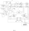
- Power factor correction circuit 20 Resonance circuit 30 First rectification filter circuit 40 Second rectification filter circuit 50 Communication circuit 60 Control system 70 Backlight module 80 Control circuit board 90 Feedback circuit 100 EMI filter circuit 110 Rectification circuit 120 Voltage division detection circuit 130 Serial bus interface socket 501 First voltage conversion circuit 502 Second voltage conversion circuit U1 Control chip U2 Control chip Q1 First electronic switch Q2 Second electronic switch T1 Transformer N1 First primary coil N2 Second primary coil N3 Second secondary coil N4 First primary coil C1 ⁇ C4 First capacitor ⁇ Fourth capacitor R1 ⁇ R9 First resistor ⁇ Ninth resistor AC AC power supply GND Ground terminal D Diode
- This application provides a power supply control circuit.
- the power supply control circuit is applied to a display device.
- the display device includes a control circuit board 80 and a backlight module 70.
- the power supply control circuit includes a power factor correction circuit 10, a resonance circuit 20, a first rectification filter circuit 30, a second rectification filter circuit 40, a communication circuit 50 and a control system 60; an output terminal of the power factor correction circuit 10 is connected to an input terminal of the resonance circuit 20; a first output terminal of the resonance circuit 20 is connected to a power input terminal of the backlight module 70 through the first rectification filter circuit 30, a second output terminal of the resonance circuit 20 is connected to a power input terminal of the control circuit board 80 through the second rectification filter circuit 40, and the second output terminal of the resonance circuit 20 is connected to a second power input terminal of the communication circuit 50 through the second rectification filter circuit 40; a third output terminal of the resonance circuit 20 is connected to a power input terminal of the control system, and the third output terminal of the resonance circuit 20 is further connected to a first power input terminal of
- control system 60 is configured to control a power factor correction (PFC) circuit and an LLC circuit (resonance circuit).
- the control system 60 may be integrated by a control system of the PFC circuit and a control system of the LLC circuit.
- the communication circuit 50 is an I2C communication circuit 50, and is configured for realizing communication connection and data transmission between the control circuit board 80 and the control system 60, so that the control circuit board 80 can read data of the control system 60 in real time or regularly, or write data to the control system 60 through the communication circuit 50.
- the power supply control circuit may further include a starting circuit, an electromagnetic interference (EMI) filter circuit 100, and a rectification circuit 110.
- the starting circuit is electrically connected to the control system 60, and the starting circuit is configured to provide a starting voltage for the control system 60 when the display device is powered on.
- An input terminal of the EMI filter circuit 100 is connected to an output terminal of an alternating current (AC) power supply
- an output terminal of the EMI filter circuit 100 is connected to an input terminal of the rectification circuit 110
- an output terminal of the rectification circuit 110 is connected to an input terminal of the power factor correction circuit 10.
- the EMI filter circuit 100 and the rectification circuit 110 are configured to filter and rectify the AC output of the AC power supply, such as 100V to 240V AC, to input to the PFC circuit 10.
- the starting circuit of the system or the external starting circuit may first provide the starting voltage for the control system 60 to start the control system 60.
- the control system 60 After the control system 60 is activated, the control system 60 generates a drive signal to a designated electronic switch in the resonance circuit 20 to control the electronic switch to turn on.
- a resonance loop composed of the conductive electronic switch, the transformer in the resonance circuit and the resonant capacitor starts to operate, and a second primary coil of the transformer of the resonance circuit 20, that is, an auxiliary winding, provides a stable voltage for the control system 60, so that the control system 60 can work normally.
- the control system 60 disconnects the connection with the starting circuit and outputs a driving signal to two electronic switches in the resonance circuit 20 to control the two electronic switches in the resonance circuit 20 to turn on alternately.
- a resonance loop composed of the electronic switches, the transformer and the resonant capacitor in the resonance circuit 20 outputs energy to a secondary circuit of the power supply through the transformer.
- one branch is filtered and rectified by the first rectification filter circuit 30 to supply power to the backlight module 70
- the other branch is filtered and rectified by the second rectification filter circuit 40 to supply power to the control circuit board 80, a screen glass, a timing control board, a power amplifier, and an external equipment, etc.
- the control circuit board 80 works normally, the control circuit board 80 outputs a dimming signal ADJ and an enable signal ENA to the backlight module 70 to light up the backlight module 70.
- the control circuit board 80 can read data in the control system 60 through the communication circuit 50, and can also write data to the control system 60 through the communication circuit 50.
- the control system 60 sets or modifies corresponding parameters of the PFC circuit 10 and the LLC circuit 20 according to the received data, that is, the control system 60 sets or modifies part of key parameters of the PFC circuit 10 and sets or modifies some key parameters of the LLC circuit 20, so as to realize, for example, such as realizing setting and modifying output ripple of a PFC boost circuit, a PFC OVP voltage and a Brownin/Brown-out voltage, realizing Burst mode frequency to the LLC circuit, over-power protection (OPP) of the LLC circuit and switching of different load LLC operating modes.
- PFP over-power protection
- the relevant design method needs to modify the device parameters of the peripheral circuit. While the power supply control circuit of this application can modify part of key parameters of the PFC circuit and LLC circuit through the control circuit board 80, without modifying the device parameters of the peripheral circuit, so that a set of power supply hardware can maximize the matching of different output and parameter setting requirements, thereby reducing the types of the material list, and facilitating production and after-sales control.
- the communication connection and data transmission between the control circuit board 80 and the control system 60 are realized through the communication circuit 50.
- the parameters in the software of the control circuit board 80 can be modified by the developer, and the modified parameters can be transmitted to the control system 60 through the communication circuit 50, the control system 60 then modifies the corresponding parameters of the power factor correction circuit 10 and the corresponding parameters of the resonance circuit 20 according to the received modified parameters.
- Such setting can maximize the matching of different output and setting requirements with a set of power supply hardware, thus reducing the types of the material list and facilitating production and after-sales control.
- the power supply control circuit further includes a feedback circuit 90, a first input terminal of the feedback circuit 90 is connected to an output terminal of the first rectification filter circuit 30, a second input terminal of the feedback circuit 90 is connected to an output terminal of the second rectification filter circuit 40, and an output terminal of the feedback circuit 90 is connected to a feedback terminal of the control system 60.
- the feedback circuit 90 is configured to detect a voltage output to the backlight module 70, detect a voltage output to the control circuit board 80, and feed back a detected voltage to the control system 60, so that the control system 60 adjusts a voltage output to a back-end circuit, thereby achieving a stable output.
- the power supply control circuit further includes an electromagnetic interference (EMI) filter circuit 100 and a rectification circuit 110, an input terminal of the EMI filter circuit 100 is connected to an output terminal of an alternating current (AC) power supply, an output terminal of the EMI filter circuit 100 is connected to an input terminal of the rectification circuit 110, and an output terminal of the rectification circuit 110 is connected to an input terminal of the power factor correction circuit 10.
- EMI electromagnetic interference
- AC alternating current
- the EMI filter circuit 100 and the rectification circuit 110 are configured to filter and rectify the AC output of the AC power supply, such as 100V to 240V AC, to input to the PFC circuit 10.
- the power supply control circuit further includes a voltage division detection circuit 120, an input terminal of the voltage division detection circuit 120 is connected to the output terminal of the EMI filter circuit 100, and an output terminal of the voltage division detection circuit 120 is connected to a voltage detection terminal of the control system 60.
- the voltage division detection circuit 120 can be realized by a plurality of resistors in series voltage division.
- the voltage division detection circuit 120 includes a seventh resistor R7 and an eighth resistor R8, a first terminal of the seventh resistor R7 is connected to the output terminal of the EMI filter circuit 100, a second terminal of the seventh resistor R7 is connected to the voltage detection terminal of the control system 60, the second terminal of the seventh resistor R7 is further connected to a first terminal of the eighth resistor R8, and a second terminal of the eighth resistor R8 is grounded.
- the voltage division detection circuit 120 detects a grid voltage filtered by the EMI filter circuit 100, and transmits the detected grid voltage to the control system 60 for the control system 60 to perform corresponding operations, for example, the voltage division detection circuit 120 transmits the detected grid voltage to the control system 60, and the control system 60 analyzes the received grid voltage by running its internal programs and modules, when the analysis finds that the grid voltage is lower than a preset voltage threshold, the control system 60 generates a control signal to control the resonance circuit 20 to stop working, to stop supplying power to the back-end circuit, so as to achieve the purpose of protecting the system.
- the communication circuit 50 includes a first voltage conversion circuit 501, a second voltage conversion circuit 502, a control chip U1, a first resistor R1, a second resistor R2, a third resistor R3, and a fourth resistor R4;
- the control chip U1 is an I2C protocol control chip.
- the first voltage conversion circuit 501 is configured to convert a voltage output from the third output terminal of the resonance circuit 20 to provide a suitable voltage for the primary of the I2C protocol control chip.
- the second voltage conversion circuit 502 is configured to convert a voltage output by the second rectification filter circuit 40 to provide a suitable voltage to the secondary of the I2C protocol control chip U1.
- the first resistor R1 is a pull-up resistor of the secondary data line SDA2 of the I2C protocol control chip
- the second resistor R2 is a pull-up resistor of the secondary clock line SCL2 of the I2C protocol control chip.
- the third resistor R3 is a pull-up resistor of the primary data line SDA1 of the I2C protocol control chip
- the fourth resistor R4 is a pull-up resistor of the primary clock line SCL1 of the I2C protocol control chip, which is used to ensure the normal transmission of data from the primary and secondary clock lines and data lines.
- the I2C protocol control chip U1 can not only realize the data transmission between the control circuit board 80 and the control system 60, but also can isolate the cold and hot ground to ensure the normal operation of the system.
- the power supply control circuit further includes a serial bus interface socket 130, pin 1 of the serial bus interface socket is grounded, pin 2 of the serial bus interface socket 130 is connected to the secondary clock line SCL2 of the control chip U1, and pin 3 of the serial bus interface socket 130 is connected to the secondary data line SDA2 of the control chip U1.
- the power supply control circuit further includes a serial bus interface socket 130, through which online information of the control system 60 is read and analyzed when the power supply malfunctions or the power supply is abnormal, so that the developer can analyze the cause of the power supply malfunction or abnormity of the power supply.
- a serial bus interface socket 130 through which online information of the control system 60 is read and analyzed when the power supply malfunctions or the power supply is abnormal, so that the developer can analyze the cause of the power supply malfunction or abnormity of the power supply.
- part of the key parameters of the primary circuit of the power supply can also be set and modified through the serial bus interface socket 130, which improves the application range of the power supply control circuit.
- the resonance circuit 20 includes a fifth resistor R5, a sixth resistor R6, a first electronic switch Q1, a second electronic switch Q2, a first capacitor C1, a second capacitor C2, a third capacitor C3, a fourth capacitor C4, a diode D, and a transformer T1;
- the starting circuit of the system may first provide the starting voltage for the control system 60 to start the control system 60.
- the control system 60 After the control system 60 starts running, the control system 60 generates a driving signal to the first electronic switch Q1 to control the first electronic switch Q1 to be turned on.
- the first electronic switch Q1 After the first electronic switch Q1 is turned on, a resonance loop composed of the first electronic switch Q1, the first primary coil N1 of the transformer T1 and the first capacitor C1 starts to work.
- the second primary coil N2 and the diode D provide a stable voltage to the control system 60 so that the control system 60 can operate normally.
- the control system 60 disconnects the connection with the starting circuit and outputs a driving signal to the first electronic switch Q1 and the second electronic switch Q2 to control the first electronic switch Q1 and the second electronic switch Q2 to turn on alternately.
- a resonance loop composed of the electronic switches, the transformer T1 and the resonant capacitor C1 in the resonance circuit 20 outputs energy to the secondary circuit through the transformer T1.
- the first electronic switch Q1 and the second electronic switch Q2 may be a transistor field effect transistor.
- the voltage division detection circuit further includes a ninth resistor R9, a first terminal of the ninth resistor R9 is connected to the output terminal of the power factor correction circuit 10, and a second terminal of the ninth resistor R9 is connected to a trigger terminal of the control system 60.
- the ninth resistor R9 is configured to provide a starting voltage to the control system 60 when the display device is powered on, so that the control system 60 can be started normally.
- This application further provides a display device including the power supply control circuit, the control circuit board 80, and the backlight module 70 according to any one of the above.
- the power supply control circuit please refer to the above-mentioned embodiments, which will not be repeated here. It is understandable that since the above-mentioned power supply control circuit is included in the display device of this application, the embodiments of the display device of this application includes all the technical solutions of the above-mentioned power supply control circuit, and the achieved technical effects are also completely the same, which will not be repeated here.
- the display device may be a display device having a display panel, such as a television, a tablet computer, or a mobile phone.
Landscapes
- Engineering & Computer Science (AREA)
- Power Engineering (AREA)
- Physics & Mathematics (AREA)
- Theoretical Computer Science (AREA)
- General Physics & Mathematics (AREA)
- General Engineering & Computer Science (AREA)
- Multimedia (AREA)
- Signal Processing (AREA)
- Computer Hardware Design (AREA)
- Electromagnetism (AREA)
- Software Systems (AREA)
- Dc-Dc Converters (AREA)
Claims (8)
- Stromversorgungssteuerschaltung für eine Anzeigevorrichtung mit einer Steuerschaltungsplatine (80) und einem Hintergrundbeleuchtungsmodul (70), wobei die Stromversorgungssteuerschaltung eine Leistungsfaktorkorrekturschaltung (10), eine Resonanzschaltung (20), eine erste Gleichrichterfilterschaltung (30), eine zweite Gleichrichterfilterschaltung (40), eine Kommunikationsschaltung (50) und ein Steuersystem (60) umfasst,wobei eine Ausgangsklemme der Leistungsfaktorkorrekturschaltung (10) an eine Eingangsklemme der Resonanzschaltung (20) angeschlossen ist; eine erste Ausgangsklemme der Resonanzschaltung (20) über die erste Gleichrichterfilterschaltung (30) an eine Leistungseingangsklemme des Hintergrundbeleuchtungsmoduls (70) angeschlossen ist, eine zweite Ausgangsklemme der Resonanzschaltung (20) über die zweite Gleichrichterfilterschaltung (40) an eine Leistungseingangsklemme der Steuerschaltungsplatine (80) angeschlossen ist, und die zweite Ausgangsklemme der Resonanzschaltung (20) über die zweite Gleichrichterfilterschaltung (40) an eine zweite Leistungseingangsklemme der Kommunikationsschaltung (50) angeschlossen ist; eine dritte Ausgangsklemme der Resonanzschaltung (20) an eine Leistungseingangsklemme des Steuersystems (60) angeschlossen ist, und die dritte Ausgangsklemme der Resonanzschaltung (20) ferner an eine erste Leistungseingangsklemme der Kommunikationsschaltung (50) verbunden; die Steuerschaltungsplatine (80) über die Kommunikationsschaltung (50) mit dem Steuersystem (60) in Kommunikationsverbindung steht; eine erste Signalausgangsklemme des Steuersystems (60) mit einem Signaleingangsklemme der Leistungsfaktorkorrekturschaltung (10) verbunden ist; und eine zweite Signalausgangsklemme des Steuersystems (60) mit einem Signaleingang der Resonanzschaltung (20) verbunden ist;wobei die Stromversorgungssteuerschaltung ferner eine Rückkopplungsschaltung (90) umfasst, wobei eine erste Eingangsklemme der Rückkopplungsschaltung (90) mit einer Ausgangsklemme der ersten Gleichrichterfilterschaltung (30) verbunden ist, eine zweite Eingangsklemme der Rückkopplungsschaltung (90) mit einer Ausgangsklemme der zweiten Gleichrichterfilterschaltung (40) verbunden ist und eine Ausgangsklemme der Rückkopplungsschaltung (90) mit einer Rückkopplungsklemme des Steuersystems (60) verbunden ist,dadurch gekennzeichnet, dass die Kommunikationsschaltung (50) eine erste Spannungsumwandlungsschaltung (501), eine zweite Spannungsumwandlungsschaltung (502), einen Steuerchip (U1), einen ersten Widerstand (R1), einen zweiten Widerstand (R2), einen dritten Widerstand (R3) und einen vierten Widerstand (R4) umfasst,wobei eine Eingangsklemme der ersten Spannungsumwandlungsschaltung (501) mit der dritten Ausgangsklemme der Resonanzschaltung (20) verbunden ist und eine erste Ausgangsklemme der ersten Spannungsumwandlungsschaltung (501) mit einer primären Stromversorgungsklemme des Steuerchips (U1) verbunden ist; eine Eingangsklemme der zweiten Spannungsumwandlungsschaltung (502) mit der Ausgangsklemme der zweiten Gleichrichterfilterschaltung (40) verbunden ist und eine erste Ausgangsklemme der zweiten Spannungsumwandlungsschaltung (502) mit einer sekundären Stromversorgungsklemme des Steuerchips (U1) verbunden ist,wobei eine primäre Datenleitung (SDA1) des Steuerchips (U1) mit einer ersten Signaleingangsklemme des Steuersystems (60) verbunden ist, und eine primäre Taktleitung (SCL1) des Steuerchips (U1) mit einer zweiten Signaleingangsklemme des Steuersystems (60) verbunden ist; eine sekundäre Datenleitung (SCL2) des Steuerchips (U1) mit einer ersten Signalausgangsklemme der Steuerschaltungsplatte (80) verbunden ist, und eine sekundäre Taktleitung (SCL2) des Steuerchips (U2) mit einer zweiten Signalausgangsklemme der Steuerschaltungsplatte (80) verbunden ist; eine erste Klemme des ersten Widerstands (R1) mit einer zweiten Ausgangsklemme der zweiten Spannungsumwandlungsschaltung (502) verbunden ist, und eine zweite Klemme des ersten Widerstands (R1) mit der sekundären Datenleitung (SDA2) des Steuerchips (U1) verbunden ist; eine erste Klemme des zweiten Widerstands (R2) mit der zweiten Ausgangsklemme der zweiten Spannungsumwandlungsschaltung (502) verbunden ist, und eine zweite Klemme des zweiten Widerstands (R2) mit der sekundären Taktleitung (SCL2) des Steuerchips (U1) verbunden ist,eine erste Klemme des dritten Widerstands (R3) mit einer zweiten Ausgangsklemme der ersten Spannungsumwandlungsschaltung (501) verbunden ist, und eine zweite Klemme des dritten Widerstands (R3) mit der primären Datenleitung (SDA1) des Steuerchips (U1) verbunden ist; und eine erste Klemme des vierten Widerstands (R4) mit der zweiten Ausgangsklemme der ersten Spannungsumwandlungsschaltung (501) verbunden ist, und eine zweite Klemme des vierten Widerstands (R4) mit der primären Taktleitung (SCL1) des Steuerchips (U1) verbunden ist.
- Stromversorgungssteuerschaltung nach Anspruch 1, wobei die Stromversorgungssteuerschaltung ferner eine serielle Bus-Schnittstellenbuchse (130) umfasst, Pin 1 der seriellen Bus-Schnittstellenbuchse (130) geerdet ist, Pin 2 der seriellen Bus-Schnittstellenbuchse (130) mit der sekundären Taktleitung (SCL2) des Steuerchips (U1) verbunden ist und Pin 3 der seriellen Bus-Schnittstellenbuchse (130) mit der sekundären Datenleitung (SDA2) des Steuerchips (U1) verbunden ist.
- Stromversorgungssteuerschaltung nach Anspruch 1, wobei die Resonanzschaltung (20) einen fünften Widerstand (R5), einen sechsten Widerstand (R6), einen ersten elektronischen Schalter (Q1), einen zweiten elektronischen Schalter (Q2), einen ersten Kondensator (C1), einen zweiten Kondensator (C2), einen dritten Kondensator (C3), einen vierten Kondensator (C4), eine Diode (D) und einen Transformator (T1) umfasst;eine gesteuerte Klemme des ersten elektronischen Schalters (Q1) über den fünften Widerstand (R5) mit einer ersten Steuerklemme des Steuersystems (60) verbunden ist, eine Eingangsklemme des ersten elektronischen Schalters (Q1) mit der Ausgangsklemme der Leistungsfaktorkorrekturschaltung (10) verbunden ist, und eine Ausgangsklemme des ersten elektronischen Schalters (Q1) mit einer Eingangsklemme des zweiten elektronischen Schalters (Q2) verbunden ist; eine gesteuerte Klemme des zweiten elektronischen Schalters (Q2) über den sechsten Widerstand (R6) mit einer zweiten Steuerklemme des Steuersystems (60) verbunden ist, und eine Ausgangsklemme des zweiten elektronischen Schalters (Q2) geerdet ist;eine gepunktete Klemme einer ersten Primärspule (N1) des Transformators (T1) mit der Ausgangsklemme des ersten elektronischen Schalters (Q1) verbunden ist, die gepunktete Klemme der ersten Primärspule (N1) des Transformators (T1) ferner mit der zweiten Signalausgangsklemme des Steuersystems (60) verbunden ist, eine nicht gepunktete Klemme der ersten Primärspule (N1) des Transformators (T1) über den zweiten Kondensator (C2) mit einem Stromerfassungsklemme des Steuersystems (60) verbunden ist, eine Klemme des ersten Kondensators (C1) mit der nicht gepunkteten Klemme der ersten Primärspule (N1) des Transformators (T1) verbunden ist und die andere Klemme des ersten Kondensators (C1) geerdet ist; eine gepunktete Klemme einer zweiten Primärspule (N2) des Transformators (T1) mit einer positiven Elektrode der Diode (D) verbunden ist und eine negative Elektrode der Diode (D) mit der Leistungseingangsklemme des Steuersystems (60) verbunden ist; eine nicht gepunktete Klemme der zweiten Primärspule (N2) des Transformators (T1) geerdet ist; eine Klemme des dritten Kondensators (C3) mit der negativen Elektrode der Diode (D) verbunden ist und die andere Klemme des dritten Kondensators (C3) geerdet ist; und eine erste Sekundärspule (N4) des Transformators (T1) mit dem Stromeingangsklemme des Hintergrundbeleuchtungsmoduls (70) über die erste Gleichrichterfilterschaltung (30) verbunden ist, und eine zweite Sekundärspule (N3) des Transformators (T1) durch die zweite Gleichrichterfilterschaltung (40) mit dem Stromeingangsklemme der Steuerschaltungsplatine (80) verbunden ist.
- Stromversorgungssteuerschaltung nach einem der Ansprüche 1 bis 3, wobei die Stromversorgungssteuerschaltung ferner eine Filterschaltung (100) für elektromagnetische Störungen (EMI) und eine Gleichrichterschaltung (110) umfasst, wobei eine Eingangsklemme der EMI-Filterschaltung (100) mit einer Ausgangsklemme einer Wechselstrom-Stromversorgung verbunden ist, wobei eine Ausgangsklemme der EMI-Filterschaltung (100) mit einer Eingangsklemme der Gleichrichterschaltung (110) verbunden ist, und wobei eine Ausgangsklemme der Gleichrichterschaltung (110) mit einer Eingangsklemme der Leistungsfaktorkorrekturschaltung (10) verbunden ist.
- Stromversorgungssteuerschaltung nach Anspruch 4, wobei die Stromversorgungssteuerschaltung ferner eine Spannungsteilungs-Erfassungsschaltung (120) umfasst, eine Eingangsklemme der Spannungsteilungs-Erfassungsschaltung (120) mit der Ausgangsklemme der EMI-Filterschaltung (100) verbunden ist und eine Ausgangsklemme der Spannungsteilungs-Erfassungsschaltung (120) mit einer Spannungserfassungsklemme des Steuersystems (60) verbunden ist.
- Stromversorgungssteuerschaltung nach Anspruch 5, wobei die Spannungsteilungs-Erfassungsschaltung (120) einen siebten Widerstand (R7) und einen achten Widerstand (R8) umfasst, wobei eine erste Klemme des siebten Widerstands (R7) mit der Ausgangsklemme der EMI-Filterschaltung (100) verbunden ist, eine zweite Klemme des siebten Widerstands (R7) mit der Spannungserfassungsklemme des Steuersystems (60) verbunden ist, die zweite Klemme des siebten Widerstands (R7) ferner mit einer ersten Klemme des achten Widerstands (R8) verbunden ist, und eine zweite Klemme des achten Widerstands (R8) geerdet ist.
- Stromversorgungssteuerschaltung nach Anspruch 6, wobei die Stromversorgungssteuerschaltung ferner einen neunten Widerstand (R9) umfasst, eine erste Klemme des neunten Widerstands (R9) mit der Ausgangsklemme der Leistungsfaktorkorrekturschaltung (10) verbunden ist und eine zweite Klemme des neunten Widerstands (R9) mit einem Triggerklemme des Steuersystems (60) verbunden ist.
- Anzeigevorrichtung, dadurch gekennzeichnet, dass die Anzeigevorrichtung eine Steuerschaltungsplatine (80), ein Hintergrundbeleuchtungsmodul (70) und die Stromversorgungssteuerschaltung nach einem der Ansprüche 1 bis 7 umfasst.
Applications Claiming Priority (2)
| Application Number | Priority Date | Filing Date | Title |
|---|---|---|---|
| CN201910845564.8A CN110620888B (zh) | 2019-09-06 | 2019-09-06 | 电源控制电路及显示装置 |
| PCT/CN2020/105552 WO2021042915A1 (zh) | 2019-09-06 | 2020-07-29 | 电源控制电路及显示装置 |
Publications (3)
| Publication Number | Publication Date |
|---|---|
| EP3934239A1 EP3934239A1 (de) | 2022-01-05 |
| EP3934239A4 EP3934239A4 (de) | 2022-12-07 |
| EP3934239B1 true EP3934239B1 (de) | 2024-06-05 |
Family
ID=68922618
Family Applications (1)
| Application Number | Title | Priority Date | Filing Date |
|---|---|---|---|
| EP20861745.6A Active EP3934239B1 (de) | 2019-09-06 | 2020-07-29 | Stromversorgungssteuerschaltung und anzeigevorrichtung |
Country Status (4)
| Country | Link |
|---|---|
| US (1) | US11670208B2 (de) |
| EP (1) | EP3934239B1 (de) |
| CN (1) | CN110620888B (de) |
| WO (1) | WO2021042915A1 (de) |
Families Citing this family (4)
| Publication number | Priority date | Publication date | Assignee | Title |
|---|---|---|---|---|
| CN110620888B (zh) | 2019-09-06 | 2021-07-20 | 深圳创维-Rgb电子有限公司 | 电源控制电路及显示装置 |
| CN115549478A (zh) * | 2021-06-30 | 2022-12-30 | 华为数字能源技术有限公司 | 一种开关变换电路和控制方法 |
| CN114552529B (zh) * | 2022-01-28 | 2022-10-21 | 绵阳惠科光电科技有限公司 | 过压保护电路、装置、显示面板及显示器 |
| CN115411953B (zh) * | 2022-10-31 | 2023-03-24 | 深圳市暗能量电源有限公司 | 一种智能家庭直流供电电源系统 |
Family Cites Families (12)
| Publication number | Priority date | Publication date | Assignee | Title |
|---|---|---|---|---|
| US6930893B2 (en) * | 2002-01-31 | 2005-08-16 | Vlt, Inc. | Factorized power architecture with point of load sine amplitude converters |
| US20120086867A1 (en) * | 2008-09-27 | 2012-04-12 | Kesler Morris P | Modular upgrades for wirelessly powered televisions |
| KR20100066603A (ko) * | 2008-12-10 | 2010-06-18 | 삼성전자주식회사 | 전원장치 및 그 제어방법 |
| CN101938222B (zh) * | 2010-07-27 | 2014-02-05 | Bcd半导体制造有限公司 | 一种供电装置和为显示装置提供背光的背光系统 |
| CN201846423U (zh) * | 2010-10-26 | 2011-05-25 | 康佳集团股份有限公司 | 用于led背光电视的电源及led背光电视 |
| DE102012011755A1 (de) * | 2012-06-12 | 2013-12-12 | Tridonic Gmbh & Co. Kg | Leistungsfaktorkorrekturschaltung, Betriebsgerät für ein Leuchtmittel und Verfahren zum Steuern einer Leistungsfaktorkorrekturschaltung |
| CN105376508B (zh) * | 2015-11-18 | 2019-03-12 | 深圳创维-Rgb电子有限公司 | 用于显示装置的大功率电源及显示装置 |
| CN106409220B (zh) * | 2016-09-29 | 2019-01-29 | 深圳创维-Rgb电子有限公司 | 一种oled驱动电源装置及oled电视 |
| KR102423070B1 (ko) * | 2017-05-02 | 2022-07-21 | 삼성전자주식회사 | 대기 상태시 오프되는 무선 전력 송신 장치 및 그 무선 전력 송신 장치를 포함하는 전자 장치 |
| CN109039052A (zh) * | 2018-10-17 | 2018-12-18 | 珠海泰通电气技术有限公司 | 基于pfc电路和谐振电路的单芯片控制电路 |
| CN109547721B (zh) * | 2018-12-25 | 2021-06-01 | 深圳创维-Rgb电子有限公司 | 一种电视电源驱动装置和电视机 |
| CN110620888B (zh) * | 2019-09-06 | 2021-07-20 | 深圳创维-Rgb电子有限公司 | 电源控制电路及显示装置 |
-
2019
- 2019-09-06 CN CN201910845564.8A patent/CN110620888B/zh active Active
-
2020
- 2020-07-29 WO PCT/CN2020/105552 patent/WO2021042915A1/zh not_active Ceased
- 2020-07-29 EP EP20861745.6A patent/EP3934239B1/de active Active
-
2021
- 2021-09-26 US US17/485,438 patent/US11670208B2/en active Active
Also Published As
| Publication number | Publication date |
|---|---|
| US11670208B2 (en) | 2023-06-06 |
| CN110620888B (zh) | 2021-07-20 |
| EP3934239A4 (de) | 2022-12-07 |
| WO2021042915A1 (zh) | 2021-03-11 |
| CN110620888A (zh) | 2019-12-27 |
| US20220013055A1 (en) | 2022-01-13 |
| EP3934239A1 (de) | 2022-01-05 |
Similar Documents
| Publication | Publication Date | Title |
|---|---|---|
| US11670208B2 (en) | Power supply control circuit and display device | |
| EP3726833B1 (de) | Fernsehnetzteilantriebsvorrichtung und fernseher | |
| US20230419916A1 (en) | Display apparatus and display control method | |
| WO2021135751A1 (zh) | 电子设备、无线充电接收装置及控制方法、无线充电系统 | |
| CN107464533A (zh) | 一种恒流驱动电路及电视机 | |
| US12332706B2 (en) | Resonant tank circuit, wide voltage input/output power supply, and electronic device | |
| WO2022041873A1 (zh) | 显示装置、阶梯供电电路 | |
| CN111697848B (zh) | 显示装置及供电控制方法 | |
| CN103051195B (zh) | 供电电路和液晶电视 | |
| CN203339978U (zh) | 液晶显示器的电源供应器 | |
| US8576585B2 (en) | Power device | |
| CN202750024U (zh) | 电源装置和等离子显示设备 | |
| US12259765B2 (en) | Power control circuit and control method thereof | |
| EP4451260A1 (de) | Anzeigevorrichtung und anzeigesteuerungsverfahren | |
| WO2024104132A1 (zh) | 一种供电设备、受电设备、芯片以及供电系统 | |
| CN112837646B (zh) | 显示装置及其控制方法 | |
| CN213602552U (zh) | 一种交直流供电电路及电视机 | |
| US20110115305A1 (en) | Electrical power-saving control apparatus, power supply including that apparatus and power-saving method thereof | |
| CN114664242A (zh) | 背光恒流控制电路及电视机 | |
| CN116317588A (zh) | 显示装置 | |
| CN102740562A (zh) | 电源控制电路、背光模组及液晶显示器件 | |
| KR20230157805A (ko) | 전자 장치 및 그 제어 방법 | |
| CN110350809B (zh) | 一种用于高速电主轴驱动器的隔离ac-dc电源 | |
| CN109151351B (zh) | 一种电源板以及电视 | |
| CN210377621U (zh) | 一种无线表决控制器 |
Legal Events
| Date | Code | Title | Description |
|---|---|---|---|
| STAA | Information on the status of an ep patent application or granted ep patent |
Free format text: STATUS: THE INTERNATIONAL PUBLICATION HAS BEEN MADE |
|
| PUAI | Public reference made under article 153(3) epc to a published international application that has entered the european phase |
Free format text: ORIGINAL CODE: 0009012 |
|
| STAA | Information on the status of an ep patent application or granted ep patent |
Free format text: STATUS: REQUEST FOR EXAMINATION WAS MADE |
|
| 17P | Request for examination filed |
Effective date: 20210928 |
|
| AK | Designated contracting states |
Kind code of ref document: A1 Designated state(s): AL AT BE BG CH CY CZ DE DK EE ES FI FR GB GR HR HU IE IS IT LI LT LU LV MC MK MT NL NO PL PT RO RS SE SI SK SM TR |
|
| A4 | Supplementary search report drawn up and despatched |
Effective date: 20221107 |
|
| RIC1 | Information provided on ipc code assigned before grant |
Ipc: G06F 1/26 20060101ALI20221101BHEP Ipc: H04N 21/443 20110101ALI20221101BHEP Ipc: H04N 5/63 20060101AFI20221101BHEP |
|
| DAV | Request for validation of the european patent (deleted) | ||
| DAX | Request for extension of the european patent (deleted) | ||
| REG | Reference to a national code |
Ref country code: DE Ref legal event code: R079 Free format text: PREVIOUS MAIN CLASS: H04N0005630000 Ipc: H02M0001420000 Ref document number: 602020032116 Country of ref document: DE |
|
| GRAP | Despatch of communication of intention to grant a patent |
Free format text: ORIGINAL CODE: EPIDOSNIGR1 |
|
| STAA | Information on the status of an ep patent application or granted ep patent |
Free format text: STATUS: GRANT OF PATENT IS INTENDED |
|
| RIC1 | Information provided on ipc code assigned before grant |
Ipc: G06F 1/26 20060101ALI20240124BHEP Ipc: H04N 5/63 20060101ALI20240124BHEP Ipc: H02M 3/335 20060101ALI20240124BHEP Ipc: H02M 3/00 20060101ALI20240124BHEP Ipc: H02M 1/42 20070101AFI20240124BHEP |
|
| INTG | Intention to grant announced |
Effective date: 20240215 |
|
| GRAS | Grant fee paid |
Free format text: ORIGINAL CODE: EPIDOSNIGR3 |
|
| GRAA | (expected) grant |
Free format text: ORIGINAL CODE: 0009210 |
|
| STAA | Information on the status of an ep patent application or granted ep patent |
Free format text: STATUS: THE PATENT HAS BEEN GRANTED |
|
| AK | Designated contracting states |
Kind code of ref document: B1 Designated state(s): AL AT BE BG CH CY CZ DE DK EE ES FI FR GB GR HR HU IE IS IT LI LT LU LV MC MK MT NL NO PL PT RO RS SE SI SK SM TR |
|
| REG | Reference to a national code |
Ref country code: CH Ref legal event code: EP |
|
| REG | Reference to a national code |
Ref country code: DE Ref legal event code: R096 Ref document number: 602020032116 Country of ref document: DE |
|
| REG | Reference to a national code |
Ref country code: IE Ref legal event code: FG4D |
|
| REG | Reference to a national code |
Ref country code: LT Ref legal event code: MG9D |
|
| PG25 | Lapsed in a contracting state [announced via postgrant information from national office to epo] |
Ref country code: BG Free format text: LAPSE BECAUSE OF FAILURE TO SUBMIT A TRANSLATION OF THE DESCRIPTION OR TO PAY THE FEE WITHIN THE PRESCRIBED TIME-LIMIT Effective date: 20240605 |
|
| REG | Reference to a national code |
Ref country code: NL Ref legal event code: MP Effective date: 20240605 |
|
| PG25 | Lapsed in a contracting state [announced via postgrant information from national office to epo] |
Ref country code: HR Free format text: LAPSE BECAUSE OF FAILURE TO SUBMIT A TRANSLATION OF THE DESCRIPTION OR TO PAY THE FEE WITHIN THE PRESCRIBED TIME-LIMIT Effective date: 20240605 Ref country code: FI Free format text: LAPSE BECAUSE OF FAILURE TO SUBMIT A TRANSLATION OF THE DESCRIPTION OR TO PAY THE FEE WITHIN THE PRESCRIBED TIME-LIMIT Effective date: 20240605 |
|
| PG25 | Lapsed in a contracting state [announced via postgrant information from national office to epo] |
Ref country code: GR Free format text: LAPSE BECAUSE OF FAILURE TO SUBMIT A TRANSLATION OF THE DESCRIPTION OR TO PAY THE FEE WITHIN THE PRESCRIBED TIME-LIMIT Effective date: 20240906 |
|
| PG25 | Lapsed in a contracting state [announced via postgrant information from national office to epo] |
Ref country code: ES Free format text: LAPSE BECAUSE OF FAILURE TO SUBMIT A TRANSLATION OF THE DESCRIPTION OR TO PAY THE FEE WITHIN THE PRESCRIBED TIME-LIMIT Effective date: 20240605 |
|
| PG25 | Lapsed in a contracting state [announced via postgrant information from national office to epo] |
Ref country code: LV Free format text: LAPSE BECAUSE OF FAILURE TO SUBMIT A TRANSLATION OF THE DESCRIPTION OR TO PAY THE FEE WITHIN THE PRESCRIBED TIME-LIMIT Effective date: 20240605 |
|
| PG25 | Lapsed in a contracting state [announced via postgrant information from national office to epo] |
Ref country code: NO Free format text: LAPSE BECAUSE OF FAILURE TO SUBMIT A TRANSLATION OF THE DESCRIPTION OR TO PAY THE FEE WITHIN THE PRESCRIBED TIME-LIMIT Effective date: 20240905 Ref country code: LV Free format text: LAPSE BECAUSE OF FAILURE TO SUBMIT A TRANSLATION OF THE DESCRIPTION OR TO PAY THE FEE WITHIN THE PRESCRIBED TIME-LIMIT Effective date: 20240605 Ref country code: HR Free format text: LAPSE BECAUSE OF FAILURE TO SUBMIT A TRANSLATION OF THE DESCRIPTION OR TO PAY THE FEE WITHIN THE PRESCRIBED TIME-LIMIT Effective date: 20240605 Ref country code: GR Free format text: LAPSE BECAUSE OF FAILURE TO SUBMIT A TRANSLATION OF THE DESCRIPTION OR TO PAY THE FEE WITHIN THE PRESCRIBED TIME-LIMIT Effective date: 20240906 Ref country code: FI Free format text: LAPSE BECAUSE OF FAILURE TO SUBMIT A TRANSLATION OF THE DESCRIPTION OR TO PAY THE FEE WITHIN THE PRESCRIBED TIME-LIMIT Effective date: 20240605 Ref country code: ES Free format text: LAPSE BECAUSE OF FAILURE TO SUBMIT A TRANSLATION OF THE DESCRIPTION OR TO PAY THE FEE WITHIN THE PRESCRIBED TIME-LIMIT Effective date: 20240605 Ref country code: BG Free format text: LAPSE BECAUSE OF FAILURE TO SUBMIT A TRANSLATION OF THE DESCRIPTION OR TO PAY THE FEE WITHIN THE PRESCRIBED TIME-LIMIT Effective date: 20240605 Ref country code: RS Free format text: LAPSE BECAUSE OF FAILURE TO SUBMIT A TRANSLATION OF THE DESCRIPTION OR TO PAY THE FEE WITHIN THE PRESCRIBED TIME-LIMIT Effective date: 20240905 |
|
| PG25 | Lapsed in a contracting state [announced via postgrant information from national office to epo] |
Ref country code: NL Free format text: LAPSE BECAUSE OF FAILURE TO SUBMIT A TRANSLATION OF THE DESCRIPTION OR TO PAY THE FEE WITHIN THE PRESCRIBED TIME-LIMIT Effective date: 20240605 |
|
| REG | Reference to a national code |
Ref country code: AT Ref legal event code: MK05 Ref document number: 1693185 Country of ref document: AT Kind code of ref document: T Effective date: 20240605 |
|
| PG25 | Lapsed in a contracting state [announced via postgrant information from national office to epo] |
Ref country code: NL Free format text: LAPSE BECAUSE OF FAILURE TO SUBMIT A TRANSLATION OF THE DESCRIPTION OR TO PAY THE FEE WITHIN THE PRESCRIBED TIME-LIMIT Effective date: 20240605 |
|
| PG25 | Lapsed in a contracting state [announced via postgrant information from national office to epo] |
Ref country code: PT Free format text: LAPSE BECAUSE OF FAILURE TO SUBMIT A TRANSLATION OF THE DESCRIPTION OR TO PAY THE FEE WITHIN THE PRESCRIBED TIME-LIMIT Effective date: 20241007 |
|
| PG25 | Lapsed in a contracting state [announced via postgrant information from national office to epo] |
Ref country code: PT Free format text: LAPSE BECAUSE OF FAILURE TO SUBMIT A TRANSLATION OF THE DESCRIPTION OR TO PAY THE FEE WITHIN THE PRESCRIBED TIME-LIMIT Effective date: 20241007 |
|
| PG25 | Lapsed in a contracting state [announced via postgrant information from national office to epo] |
Ref country code: PL Free format text: LAPSE BECAUSE OF FAILURE TO SUBMIT A TRANSLATION OF THE DESCRIPTION OR TO PAY THE FEE WITHIN THE PRESCRIBED TIME-LIMIT Effective date: 20240605 |
|
| PG25 | Lapsed in a contracting state [announced via postgrant information from national office to epo] |
Ref country code: EE Free format text: LAPSE BECAUSE OF FAILURE TO SUBMIT A TRANSLATION OF THE DESCRIPTION OR TO PAY THE FEE WITHIN THE PRESCRIBED TIME-LIMIT Effective date: 20240605 |
|
| PG25 | Lapsed in a contracting state [announced via postgrant information from national office to epo] |
Ref country code: AT Free format text: LAPSE BECAUSE OF FAILURE TO SUBMIT A TRANSLATION OF THE DESCRIPTION OR TO PAY THE FEE WITHIN THE PRESCRIBED TIME-LIMIT Effective date: 20240605 Ref country code: IS Free format text: LAPSE BECAUSE OF FAILURE TO SUBMIT A TRANSLATION OF THE DESCRIPTION OR TO PAY THE FEE WITHIN THE PRESCRIBED TIME-LIMIT Effective date: 20241005 |
|
| PG25 | Lapsed in a contracting state [announced via postgrant information from national office to epo] |
Ref country code: CZ Free format text: LAPSE BECAUSE OF FAILURE TO SUBMIT A TRANSLATION OF THE DESCRIPTION OR TO PAY THE FEE WITHIN THE PRESCRIBED TIME-LIMIT Effective date: 20240605 |
|
| PG25 | Lapsed in a contracting state [announced via postgrant information from national office to epo] |
Ref country code: SK Free format text: LAPSE BECAUSE OF FAILURE TO SUBMIT A TRANSLATION OF THE DESCRIPTION OR TO PAY THE FEE WITHIN THE PRESCRIBED TIME-LIMIT Effective date: 20240605 Ref country code: RO Free format text: LAPSE BECAUSE OF FAILURE TO SUBMIT A TRANSLATION OF THE DESCRIPTION OR TO PAY THE FEE WITHIN THE PRESCRIBED TIME-LIMIT Effective date: 20240605 |
|
| PG25 | Lapsed in a contracting state [announced via postgrant information from national office to epo] |
Ref country code: SM Free format text: LAPSE BECAUSE OF FAILURE TO SUBMIT A TRANSLATION OF THE DESCRIPTION OR TO PAY THE FEE WITHIN THE PRESCRIBED TIME-LIMIT Effective date: 20240605 |
|
| PG25 | Lapsed in a contracting state [announced via postgrant information from national office to epo] |
Ref country code: SM Free format text: LAPSE BECAUSE OF FAILURE TO SUBMIT A TRANSLATION OF THE DESCRIPTION OR TO PAY THE FEE WITHIN THE PRESCRIBED TIME-LIMIT Effective date: 20240605 Ref country code: SK Free format text: LAPSE BECAUSE OF FAILURE TO SUBMIT A TRANSLATION OF THE DESCRIPTION OR TO PAY THE FEE WITHIN THE PRESCRIBED TIME-LIMIT Effective date: 20240605 Ref country code: RO Free format text: LAPSE BECAUSE OF FAILURE TO SUBMIT A TRANSLATION OF THE DESCRIPTION OR TO PAY THE FEE WITHIN THE PRESCRIBED TIME-LIMIT Effective date: 20240605 Ref country code: PL Free format text: LAPSE BECAUSE OF FAILURE TO SUBMIT A TRANSLATION OF THE DESCRIPTION OR TO PAY THE FEE WITHIN THE PRESCRIBED TIME-LIMIT Effective date: 20240605 Ref country code: IS Free format text: LAPSE BECAUSE OF FAILURE TO SUBMIT A TRANSLATION OF THE DESCRIPTION OR TO PAY THE FEE WITHIN THE PRESCRIBED TIME-LIMIT Effective date: 20241005 Ref country code: EE Free format text: LAPSE BECAUSE OF FAILURE TO SUBMIT A TRANSLATION OF THE DESCRIPTION OR TO PAY THE FEE WITHIN THE PRESCRIBED TIME-LIMIT Effective date: 20240605 Ref country code: CZ Free format text: LAPSE BECAUSE OF FAILURE TO SUBMIT A TRANSLATION OF THE DESCRIPTION OR TO PAY THE FEE WITHIN THE PRESCRIBED TIME-LIMIT Effective date: 20240605 Ref country code: AT Free format text: LAPSE BECAUSE OF FAILURE TO SUBMIT A TRANSLATION OF THE DESCRIPTION OR TO PAY THE FEE WITHIN THE PRESCRIBED TIME-LIMIT Effective date: 20240605 |
|
| REG | Reference to a national code |
Ref country code: CH Ref legal event code: PL |
|
| REG | Reference to a national code |
Ref country code: DE Ref legal event code: R097 Ref document number: 602020032116 Country of ref document: DE |
|
| PG25 | Lapsed in a contracting state [announced via postgrant information from national office to epo] |
Ref country code: LU Free format text: LAPSE BECAUSE OF NON-PAYMENT OF DUE FEES Effective date: 20240729 |
|
| PG25 | Lapsed in a contracting state [announced via postgrant information from national office to epo] |
Ref country code: MC Free format text: LAPSE BECAUSE OF FAILURE TO SUBMIT A TRANSLATION OF THE DESCRIPTION OR TO PAY THE FEE WITHIN THE PRESCRIBED TIME-LIMIT Effective date: 20240605 |
|
| PG25 | Lapsed in a contracting state [announced via postgrant information from national office to epo] |
Ref country code: MC Free format text: LAPSE BECAUSE OF FAILURE TO SUBMIT A TRANSLATION OF THE DESCRIPTION OR TO PAY THE FEE WITHIN THE PRESCRIBED TIME-LIMIT Effective date: 20240605 Ref country code: LU Free format text: LAPSE BECAUSE OF NON-PAYMENT OF DUE FEES Effective date: 20240729 |
|
| PLBE | No opposition filed within time limit |
Free format text: ORIGINAL CODE: 0009261 |
|
| STAA | Information on the status of an ep patent application or granted ep patent |
Free format text: STATUS: NO OPPOSITION FILED WITHIN TIME LIMIT |
|
| PG25 | Lapsed in a contracting state [announced via postgrant information from national office to epo] |
Ref country code: DK Free format text: LAPSE BECAUSE OF FAILURE TO SUBMIT A TRANSLATION OF THE DESCRIPTION OR TO PAY THE FEE WITHIN THE PRESCRIBED TIME-LIMIT Effective date: 20240605 |
|
| PG25 | Lapsed in a contracting state [announced via postgrant information from national office to epo] |
Ref country code: CH Free format text: LAPSE BECAUSE OF NON-PAYMENT OF DUE FEES Effective date: 20240731 Ref country code: BE Free format text: LAPSE BECAUSE OF NON-PAYMENT OF DUE FEES Effective date: 20240731 |
|
| 26N | No opposition filed |
Effective date: 20250306 |
|
| REG | Reference to a national code |
Ref country code: BE Ref legal event code: MM Effective date: 20240731 |
|
| PG25 | Lapsed in a contracting state [announced via postgrant information from national office to epo] |
Ref country code: IE Free format text: LAPSE BECAUSE OF NON-PAYMENT OF DUE FEES Effective date: 20240729 |
|
| PG25 | Lapsed in a contracting state [announced via postgrant information from national office to epo] |
Ref country code: SE Free format text: LAPSE BECAUSE OF FAILURE TO SUBMIT A TRANSLATION OF THE DESCRIPTION OR TO PAY THE FEE WITHIN THE PRESCRIBED TIME-LIMIT Effective date: 20240605 |
|
| PGFP | Annual fee paid to national office [announced via postgrant information from national office to epo] |
Ref country code: DE Payment date: 20250812 Year of fee payment: 6 |
|
| PGFP | Annual fee paid to national office [announced via postgrant information from national office to epo] |
Ref country code: IT Payment date: 20250710 Year of fee payment: 6 |
|
| PGFP | Annual fee paid to national office [announced via postgrant information from national office to epo] |
Ref country code: GB Payment date: 20250826 Year of fee payment: 6 |
|
| PGFP | Annual fee paid to national office [announced via postgrant information from national office to epo] |
Ref country code: FR Payment date: 20250731 Year of fee payment: 6 |
|
| PG25 | Lapsed in a contracting state [announced via postgrant information from national office to epo] |
Ref country code: CY Free format text: LAPSE BECAUSE OF FAILURE TO SUBMIT A TRANSLATION OF THE DESCRIPTION OR TO PAY THE FEE WITHIN THE PRESCRIBED TIME-LIMIT; INVALID AB INITIO Effective date: 20200729 |
|
| PG25 | Lapsed in a contracting state [announced via postgrant information from national office to epo] |
Ref country code: HU Free format text: LAPSE BECAUSE OF FAILURE TO SUBMIT A TRANSLATION OF THE DESCRIPTION OR TO PAY THE FEE WITHIN THE PRESCRIBED TIME-LIMIT; INVALID AB INITIO Effective date: 20200729 |