EP3933886A1 - Method for manufacturing semiconductor element and semiconductor element body - Google Patents
Method for manufacturing semiconductor element and semiconductor element body Download PDFInfo
- Publication number
- EP3933886A1 EP3933886A1 EP20762528.6A EP20762528A EP3933886A1 EP 3933886 A1 EP3933886 A1 EP 3933886A1 EP 20762528 A EP20762528 A EP 20762528A EP 3933886 A1 EP3933886 A1 EP 3933886A1
- Authority
- EP
- European Patent Office
- Prior art keywords
- semiconductor element
- support substrate
- substrate
- underlying
- underlying substrate
- Prior art date
- Legal status (The legal status is an assumption and is not a legal conclusion. Google has not performed a legal analysis and makes no representation as to the accuracy of the status listed.)
- Granted
Links
Images










Classifications
-
- H—ELECTRICITY
- H10—SEMICONDUCTOR DEVICES; ELECTRIC SOLID-STATE DEVICES NOT OTHERWISE PROVIDED FOR
- H10P—GENERIC PROCESSES OR APPARATUS FOR THE MANUFACTURE OR TREATMENT OF DEVICES COVERED BY CLASS H10
- H10P95/00—Generic processes or apparatus for manufacture or treatments not covered by the other groups of this subclass
- H10P95/11—Separation of active layers from substrates
- H10P95/112—Separation of active layers from substrates leaving a reusable substrate, e.g. epitaxial lift off
-
- H—ELECTRICITY
- H10—SEMICONDUCTOR DEVICES; ELECTRIC SOLID-STATE DEVICES NOT OTHERWISE PROVIDED FOR
- H10P—GENERIC PROCESSES OR APPARATUS FOR THE MANUFACTURE OR TREATMENT OF DEVICES COVERED BY CLASS H10
- H10P54/00—Cutting or separating of wafers, substrates or parts of devices
-
- H—ELECTRICITY
- H10—SEMICONDUCTOR DEVICES; ELECTRIC SOLID-STATE DEVICES NOT OTHERWISE PROVIDED FOR
- H10H—INORGANIC LIGHT-EMITTING SEMICONDUCTOR DEVICES HAVING POTENTIAL BARRIERS
- H10H20/00—Individual inorganic light-emitting semiconductor devices having potential barriers, e.g. light-emitting diodes [LED]
- H10H20/01—Manufacture or treatment
- H10H20/011—Manufacture or treatment of bodies, e.g. forming semiconductor layers
- H10H20/018—Bonding of wafers
-
- H—ELECTRICITY
- H10—SEMICONDUCTOR DEVICES; ELECTRIC SOLID-STATE DEVICES NOT OTHERWISE PROVIDED FOR
- H10W—GENERIC PACKAGES, INTERCONNECTIONS, CONNECTORS OR OTHER CONSTRUCTIONAL DETAILS OF DEVICES COVERED BY CLASS H10
- H10W72/00—Interconnections or connectors in packages
-
- H—ELECTRICITY
- H10—SEMICONDUCTOR DEVICES; ELECTRIC SOLID-STATE DEVICES NOT OTHERWISE PROVIDED FOR
- H10H—INORGANIC LIGHT-EMITTING SEMICONDUCTOR DEVICES HAVING POTENTIAL BARRIERS
- H10H20/00—Individual inorganic light-emitting semiconductor devices having potential barriers, e.g. light-emitting diodes [LED]
- H10H20/01—Manufacture or treatment
- H10H20/011—Manufacture or treatment of bodies, e.g. forming semiconductor layers
- H10H20/013—Manufacture or treatment of bodies, e.g. forming semiconductor layers having light-emitting regions comprising only Group III-V materials
- H10H20/0133—Manufacture or treatment of bodies, e.g. forming semiconductor layers having light-emitting regions comprising only Group III-V materials with a substrate not being Group III-V materials
- H10H20/01335—Manufacture or treatment of bodies, e.g. forming semiconductor layers having light-emitting regions comprising only Group III-V materials with a substrate not being Group III-V materials the light-emitting regions comprising nitride materials
-
- H—ELECTRICITY
- H10—SEMICONDUCTOR DEVICES; ELECTRIC SOLID-STATE DEVICES NOT OTHERWISE PROVIDED FOR
- H10H—INORGANIC LIGHT-EMITTING SEMICONDUCTOR DEVICES HAVING POTENTIAL BARRIERS
- H10H20/00—Individual inorganic light-emitting semiconductor devices having potential barriers, e.g. light-emitting diodes [LED]
- H10H20/01—Manufacture or treatment
- H10H20/011—Manufacture or treatment of bodies, e.g. forming semiconductor layers
- H10H20/013—Manufacture or treatment of bodies, e.g. forming semiconductor layers having light-emitting regions comprising only Group III-V materials
- H10H20/0137—Manufacture or treatment of bodies, e.g. forming semiconductor layers having light-emitting regions comprising only Group III-V materials the light-emitting regions comprising nitride materials
-
- H—ELECTRICITY
- H10—SEMICONDUCTOR DEVICES; ELECTRIC SOLID-STATE DEVICES NOT OTHERWISE PROVIDED FOR
- H10H—INORGANIC LIGHT-EMITTING SEMICONDUCTOR DEVICES HAVING POTENTIAL BARRIERS
- H10H20/00—Individual inorganic light-emitting semiconductor devices having potential barriers, e.g. light-emitting diodes [LED]
- H10H20/01—Manufacture or treatment
- H10H20/032—Manufacture or treatment of electrodes
-
- H—ELECTRICITY
- H10—SEMICONDUCTOR DEVICES; ELECTRIC SOLID-STATE DEVICES NOT OTHERWISE PROVIDED FOR
- H10H—INORGANIC LIGHT-EMITTING SEMICONDUCTOR DEVICES HAVING POTENTIAL BARRIERS
- H10H20/00—Individual inorganic light-emitting semiconductor devices having potential barriers, e.g. light-emitting diodes [LED]
- H10H20/80—Constructional details
- H10H20/83—Electrodes
- H10H20/832—Electrodes characterised by their material
-
- H—ELECTRICITY
- H10—SEMICONDUCTOR DEVICES; ELECTRIC SOLID-STATE DEVICES NOT OTHERWISE PROVIDED FOR
- H10P—GENERIC PROCESSES OR APPARATUS FOR THE MANUFACTURE OR TREATMENT OF DEVICES COVERED BY CLASS H10
- H10P14/00—Formation of materials, e.g. in the shape of layers or pillars
- H10P14/20—Formation of materials, e.g. in the shape of layers or pillars of semiconductor materials
- H10P14/27—Formation of materials, e.g. in the shape of layers or pillars of semiconductor materials using selective deposition, e.g. simultaneous growth of monocrystalline and non-monocrystalline semiconductor materials
- H10P14/276—Lateral overgrowth
-
- H—ELECTRICITY
- H10—SEMICONDUCTOR DEVICES; ELECTRIC SOLID-STATE DEVICES NOT OTHERWISE PROVIDED FOR
- H10P—GENERIC PROCESSES OR APPARATUS FOR THE MANUFACTURE OR TREATMENT OF DEVICES COVERED BY CLASS H10
- H10P14/00—Formation of materials, e.g. in the shape of layers or pillars
- H10P14/20—Formation of materials, e.g. in the shape of layers or pillars of semiconductor materials
- H10P14/29—Formation of materials, e.g. in the shape of layers or pillars of semiconductor materials characterised by the substrates
- H10P14/2901—Materials
- H10P14/2902—Materials being Group IVA materials
- H10P14/2905—Silicon, silicon germanium or germanium
-
- H—ELECTRICITY
- H10—SEMICONDUCTOR DEVICES; ELECTRIC SOLID-STATE DEVICES NOT OTHERWISE PROVIDED FOR
- H10P—GENERIC PROCESSES OR APPARATUS FOR THE MANUFACTURE OR TREATMENT OF DEVICES COVERED BY CLASS H10
- H10P14/00—Formation of materials, e.g. in the shape of layers or pillars
- H10P14/20—Formation of materials, e.g. in the shape of layers or pillars of semiconductor materials
- H10P14/29—Formation of materials, e.g. in the shape of layers or pillars of semiconductor materials characterised by the substrates
- H10P14/2901—Materials
- H10P14/2907—Materials being Group IIIA-VA materials
- H10P14/2908—Nitrides
-
- H—ELECTRICITY
- H10—SEMICONDUCTOR DEVICES; ELECTRIC SOLID-STATE DEVICES NOT OTHERWISE PROVIDED FOR
- H10P—GENERIC PROCESSES OR APPARATUS FOR THE MANUFACTURE OR TREATMENT OF DEVICES COVERED BY CLASS H10
- H10P14/00—Formation of materials, e.g. in the shape of layers or pillars
- H10P14/20—Formation of materials, e.g. in the shape of layers or pillars of semiconductor materials
- H10P14/29—Formation of materials, e.g. in the shape of layers or pillars of semiconductor materials characterised by the substrates
- H10P14/2926—Crystal orientations
-
- H—ELECTRICITY
- H10—SEMICONDUCTOR DEVICES; ELECTRIC SOLID-STATE DEVICES NOT OTHERWISE PROVIDED FOR
- H10W—GENERIC PACKAGES, INTERCONNECTIONS, CONNECTORS OR OTHER CONSTRUCTIONAL DETAILS OF DEVICES COVERED BY CLASS H10
- H10W72/00—Interconnections or connectors in packages
- H10W72/01—Manufacture or treatment
- H10W72/019—Manufacture or treatment of bond pads
-
- H—ELECTRICITY
- H10—SEMICONDUCTOR DEVICES; ELECTRIC SOLID-STATE DEVICES NOT OTHERWISE PROVIDED FOR
- H10W—GENERIC PACKAGES, INTERCONNECTIONS, CONNECTORS OR OTHER CONSTRUCTIONAL DETAILS OF DEVICES COVERED BY CLASS H10
- H10W72/00—Interconnections or connectors in packages
- H10W72/01—Manufacture or treatment
- H10W72/019—Manufacture or treatment of bond pads
- H10W72/01951—Changing the shapes of bond pads
-
- H—ELECTRICITY
- H10—SEMICONDUCTOR DEVICES; ELECTRIC SOLID-STATE DEVICES NOT OTHERWISE PROVIDED FOR
- H10W—GENERIC PACKAGES, INTERCONNECTIONS, CONNECTORS OR OTHER CONSTRUCTIONAL DETAILS OF DEVICES COVERED BY CLASS H10
- H10W72/00—Interconnections or connectors in packages
- H10W72/01—Manufacture or treatment
- H10W72/019—Manufacture or treatment of bond pads
- H10W72/01951—Changing the shapes of bond pads
- H10W72/01955—Changing the shapes of bond pads by using masks
-
- H—ELECTRICITY
- H10—SEMICONDUCTOR DEVICES; ELECTRIC SOLID-STATE DEVICES NOT OTHERWISE PROVIDED FOR
- H10W—GENERIC PACKAGES, INTERCONNECTIONS, CONNECTORS OR OTHER CONSTRUCTIONAL DETAILS OF DEVICES COVERED BY CLASS H10
- H10W72/00—Interconnections or connectors in packages
- H10W72/01—Manufacture or treatment
- H10W72/0198—Manufacture or treatment batch processes
-
- H—ELECTRICITY
- H10—SEMICONDUCTOR DEVICES; ELECTRIC SOLID-STATE DEVICES NOT OTHERWISE PROVIDED FOR
- H10W—GENERIC PACKAGES, INTERCONNECTIONS, CONNECTORS OR OTHER CONSTRUCTIONAL DETAILS OF DEVICES COVERED BY CLASS H10
- H10W72/00—Interconnections or connectors in packages
- H10W72/071—Connecting or disconnecting
- H10W72/072—Connecting or disconnecting of bump connectors
- H10W72/07231—Techniques
- H10W72/07236—Soldering or alloying
-
- H—ELECTRICITY
- H10—SEMICONDUCTOR DEVICES; ELECTRIC SOLID-STATE DEVICES NOT OTHERWISE PROVIDED FOR
- H10W—GENERIC PACKAGES, INTERCONNECTIONS, CONNECTORS OR OTHER CONSTRUCTIONAL DETAILS OF DEVICES COVERED BY CLASS H10
- H10W72/00—Interconnections or connectors in packages
- H10W72/90—Bond pads, in general
-
- H—ELECTRICITY
- H10—SEMICONDUCTOR DEVICES; ELECTRIC SOLID-STATE DEVICES NOT OTHERWISE PROVIDED FOR
- H10W—GENERIC PACKAGES, INTERCONNECTIONS, CONNECTORS OR OTHER CONSTRUCTIONAL DETAILS OF DEVICES COVERED BY CLASS H10
- H10W72/00—Interconnections or connectors in packages
- H10W72/90—Bond pads, in general
- H10W72/921—Structures or relative sizes of bond pads
- H10W72/923—Bond pads having multiple stacked layers
-
- H—ELECTRICITY
- H10—SEMICONDUCTOR DEVICES; ELECTRIC SOLID-STATE DEVICES NOT OTHERWISE PROVIDED FOR
- H10W—GENERIC PACKAGES, INTERCONNECTIONS, CONNECTORS OR OTHER CONSTRUCTIONAL DETAILS OF DEVICES COVERED BY CLASS H10
- H10W72/00—Interconnections or connectors in packages
- H10W72/90—Bond pads, in general
- H10W72/931—Shapes of bond pads
-
- H—ELECTRICITY
- H10—SEMICONDUCTOR DEVICES; ELECTRIC SOLID-STATE DEVICES NOT OTHERWISE PROVIDED FOR
- H10W—GENERIC PACKAGES, INTERCONNECTIONS, CONNECTORS OR OTHER CONSTRUCTIONAL DETAILS OF DEVICES COVERED BY CLASS H10
- H10W72/00—Interconnections or connectors in packages
- H10W72/90—Bond pads, in general
- H10W72/951—Materials of bond pads
- H10W72/952—Materials of bond pads comprising metals or metalloids, e.g. PbSn, Ag or Cu
-
- H—ELECTRICITY
- H10—SEMICONDUCTOR DEVICES; ELECTRIC SOLID-STATE DEVICES NOT OTHERWISE PROVIDED FOR
- H10W—GENERIC PACKAGES, INTERCONNECTIONS, CONNECTORS OR OTHER CONSTRUCTIONAL DETAILS OF DEVICES COVERED BY CLASS H10
- H10W80/00—Direct bonding of chips, wafers or substrates
- H10W80/701—Direct bonding of chips, wafers or substrates characterised by the pads after the direct bonding
-
- H—ELECTRICITY
- H10—SEMICONDUCTOR DEVICES; ELECTRIC SOLID-STATE DEVICES NOT OTHERWISE PROVIDED FOR
- H10W—GENERIC PACKAGES, INTERCONNECTIONS, CONNECTORS OR OTHER CONSTRUCTIONAL DETAILS OF DEVICES COVERED BY CLASS H10
- H10W90/00—Package configurations
- H10W90/701—Package configurations characterised by the relative positions of pads or connectors relative to package parts
- H10W90/791—Package configurations characterised by the relative positions of pads or connectors relative to package parts of direct-bonded pads
- H10W90/792—Package configurations characterised by the relative positions of pads or connectors relative to package parts of direct-bonded pads between multiple chips
Definitions
- the present disclosure relates to a method of manufacturing a semiconductor element, and a semiconductor element body.
- Patent Document 1 A method of manufacturing a semiconductor element according to a related art is described, for example, in Patent Document 1.
- Patent Document 1 JP 4638958 B
- a method of manufacturing a semiconductor element according to the present disclosure may include an element forming step of forming, on an underlying substrate, a semiconductor element connected to the underlying substrate via a connecting portion and including an upper surface inclined with respect to a growth surface of the underlying substrate, a preparing step of preparing a support substrate including an opposing surface caused to face the underlying substrate, a bonding step of pressing the upper surface of the semiconductor element against the opposing surface of the support substrate and heating the upper surface to bond the upper surface of the semiconductor element to the support substrate, and a peeling step of peeling the semiconductor element from the underlying substrate.
- a method of manufacturing a semiconductor element according to the present disclosure may include an element forming step of forming, on an underlying substrate, a semiconductor element connected to the underlying substrate via a connecting portion, a preparing step of preparing a support substrate including an opposing surface inclined with respect to a growth surface of the underlying substrate when the support substrate is caused to face the underlying substrate, a bonding step of pressing an upper surface of the semiconductor element against the opposing surface of the support substrate and heating the upper surface to bond the upper surface of the semiconductor element to the support substrate, and a peeling step of peeling the semiconductor element from the underlying substrate.
- a method of manufacturing a semiconductor element according to the present disclosure may include an element forming step of forming, on an underlying substrate, a semiconductor element connected to the underlying substrate via a connecting portion, a preparing step of preparing a support substrate including an opposing surface caused to face the underlying substrate, the opposing surface including a stepped portion, a bonding step of pressing an upper surface of the semiconductor element against the opposing surface of the support substrate such that the upper surface of the semiconductor element and the stepped portion of the opposing surface of the support substrate come into contact with each other, and heating the upper surface, to bond the upper surface of the semiconductor element to the support substrate, and a peeling step of peeling the semiconductor element from the underlying substrate.
- a semiconductor element body of the present disclosure may include a support substrate and a semiconductor element layer including a first surface and a second surface located on an opposite side to the first surface, wherein a side with the first surface is fixed to the support substrate, and the second surface is inclined with respect to a surface of the support substrate.
- a semiconductor element body of the present disclosure may include a support substrate including an inclined surface, and a semiconductor element layer including a first surface and a second surface located on an opposite side to the first surface, wherein a side with the first surface is fixed to the inclined surface of the support substrate.
- a semiconductor element body of the present disclosure may include a support substrate and a semiconductor element including a first surface and a second surface located on an opposite side to the first surface, wherein a side with the first surface is fixed to the support substrate, at least the first surface of the first surface and the second surface is inclined with respect to a surface of the support substrate.
- the yield of the semiconductor element can be increased.
- the semiconductor element body of the present disclosure separation into individual semiconductor elements is facilitated, so that the yield of the semiconductor element can be increased.
- a mask having a stripe-shaped slit is formed on an underlying substrate made of sapphire, gallium nitride (GaN), or the like. Then, a semiconductor is epitaxially grown from the substrate exposed from the slit, and the formed semiconductor element is transferred to a support substrate.
- GaN gallium nitride
- the semiconductor element when transferring the grown semiconductor element to the support substrate, after the semiconductor element is bonded to the support substrate, a force in a direction perpendicular to each surface of the underlying substrate and the support substrate is applied to break the connecting portion between the underlying substrate and the semiconductor element. At this time, when a force is applied between the support substrate and the semiconductor element, an electrode of the semiconductor element may be peeled off, and this leads to a high possibility of the semiconductor element not being reliably transferred to the support substrate, for example. Thus, the yield of the semiconductor element may not be improved.
- FIG. 1 is a basic process diagram of a method of manufacturing a semiconductor element according to an embodiment of the present disclosure.
- a method of manufacturing a semiconductor element according to the present disclosure includes an element forming step S1 of forming a semiconductor element on an underlying substrate, a preparing step S2 of preparing a support substrate, a bonding step S3 of bonding the semiconductor element on the underlying substrate to the support substrate, and a peeling step S4 of peeling the semiconductor element from the underlying substrate.
- the element forming step S1 and the preparing step S2 need not be performed in this order, and for example, the element forming step S1 and the preparing step S2 may be performed in parallel.
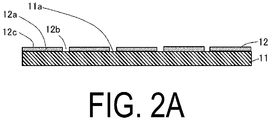
- FIGS. 2A to 2C are cross-sectional views illustrating the element forming step according to the first embodiment.
- an underlying substrate 11 is prepared.
- a GaN template substrate is used as the underlying substrate 11.
- the underlying substrate 11 is an off-angle substrate, and a normal direction of a growth surface 11a of the underlying substrate 11 (or the surface perpendicular to a thickness direction of the underlying substrate 11) is inclined by 0.3° from an a axis ( ⁇ 11-20 >) direction.
- the off angle with respect to the a axis is 0.3°; however, a substrate having an off angle of from 0.1° to 1°, in other words, a substrate in which the growth surface 11a of the underlying substrate 11 is a crystal plane having an off angle with respect to the normal line of the growth surface 11a can be used.
- a substrate having an off angle of from 0.1° to 1° in other words, a substrate in which the growth surface 11a of the underlying substrate 11 is a crystal plane having an off angle with respect to the normal line of the growth surface 11a can be used.
- the underlying substrate 11 for example, a GaN substrate cut out from a GaN single crystal ingot so that the growth surface 11a of the underlying substrate is in a predetermined plane direction can be used.
- any nitride semiconductor substrate may be used.
- an n-type substrate or a p-type substrate in which the nitride semiconductor is doped with impurities may be used.
- the GaN template substrate for example, sapphire, Si, or SiC can be used.
- a mask 12 is formed on the underlying substrate 11.
- a silicon oxide for example, SiO 2 or the like
- a SiO 2 layer of approximately 100 nm is layered on the growth surface 11a.
- the SiO 2 layer is patterned by a photolithography method and wet etching using buffered hydrogen fluoride (BHF) to form the mask 12 illustrated in FIG. 2A .
- BHF buffered hydrogen fluoride
- the mask 12 has a stripe shape in which a plurality of strip-shaped portions 12a are arranged in parallel at a predetermined interval.
- a width of an opening portion 12b between adjacent strip-shaped portions 12a is, for example, approximately 5 ⁇ m.
- a width of each strip-shaped portion 12a is, for example, from approximately 50 ⁇ m to approximately 200 ⁇ m.
- the width of the opening portion 12b is, for example, from approximately 2 ⁇ m to approximately 20 ⁇ m.
- the mask material for forming the mask 12 may be, in addition to SiO 2 , a material in which a semiconductor layer does not grow from the mask material by vapor phase epitaxy.
- a material in which a semiconductor layer does not grow from the mask material by vapor phase epitaxy for example, an oxide, such as ZrOx, TiOx, or AlOx, which can be patterned, or a transition metal, such as W or Cr can also be used.
- any method of layering the mask layer any method, such as vapor deposition, sputtering, or coating and curing, which are suitable for the mask material, can be used as appropriate.
- a semiconductor element layer 13 which is a crystal growth layer of a semiconductor crystal, is vapor phase grown from the growth surface 11a exposed from the opening portion 12b.
- the semiconductor element layer 13 of the present disclosure is a nitride semiconductor layer.
- VPE vapor phase epitaxy
- MOCVD metal organic chemical vapor deposition
- the semiconductor element layer 13 which is a nitride semiconductor grown by an epitaxial lateral overgrowth (ELO) method, is obtained.
- the width of the semiconductor element layer 13 is, for example, from approximately 50 ⁇ m to approximately 200 ⁇ m, and the height is from approximately 10 ⁇ m to approximately 50 ⁇ m.
- FIG. 3 is a photograph of the semiconductor element layer formed on the underlying substrate, and is a top view of the semiconductor element layer formed on the mask by the above-described method.
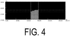
- FIG. 4 is a graph showing an inclination of the upper surface of the semiconductor element layer, showing a measurement result of measuring a distance between the upper surface of the semiconductor element layer illustrated in FIG. 3 and a reference surface.
- a width W of the semiconductor element layer 13 formed in a strip shape is 35 ⁇ m, and in the width direction, the right end side is higher than the left end side, and the height difference between both ends is 150 nm.
- An inclination angle of a first surface 13a (upper surface) of the semiconductor element layer 13 is 0.25°.
- the off angle of the underlying substrate 11 used in the growth of the semiconductor element layer 13 is 0.22°, and the inclination angle of the first surface 13a corresponds to the off angle of the underlying substrate 11.
- Growing the semiconductor element layer 13 with the off angle on the underlying substrate 11 in this manner is advantageous for realizing the semiconductor element layer 13 of a crystal having excellent quality.
- the semiconductor element layer 13 has the first surface 13a and a second surface 13c located on the opposite side to the first surface 13a.
- a metal layer 14 is formed on the first surface 13a of the semiconductor element layer 13, as illustrated in FIG. 2B .
- the entire upper surface of the underlying substrate 11, the mask 12, and the semiconductor element layer 13 is covered with a resist film.
- an opening portion is provided using a photolithography method so that the first surface 13a of the semiconductor element layer 13 is exposed.
- a Cr layer and a AuSn layer which is an alloy of gold and tin, are vapor deposited in order in the opening portion.
- the unnecessary metal layer is removed together with the resist film by a lift-off method to form the metal layer 14.
- the thickness of the metal layer is from approximately 1 ⁇ m to approximately 5 ⁇ m.
- the underlying substrate 11, the mask 12 formed on the underlying substrate 11, the semiconductor element layer 13, and the metal layer 14 are immersed in BHF for approximately 10 minutes to remove the mask 12.
- a semiconductor element 15 is formed on the underlying substrate 11.
- the semiconductor element 15 and the underlying substrate 11 are connected to each other via, for example, a connecting portion 13b having a columnar shape, which is a portion of the semiconductor element layer 13 grown in the opening portion 12b of the mask 12.
- the metal layer 14 can be used as an electrode of the semiconductor element 15. However, depending on the configuration of the semiconductor element 15, the metal layer 14 need not necessarily be used as the electrode.
- An upper surface 15a of the semiconductor element 15 is inclined similarly to the first surface 13a of the semiconductor element layer 13.
- the semiconductor element layer 13 has the first surface 13a and the second surface 13c located on the opposite side to the first surface 13a.
- FIG. 5 is a cross-sectional view illustrating a preparing step according to the first embodiment.
- a support substrate 16 for connecting to the semiconductor element 15 is prepared.
- a silicon substrate is used as a base 16a.
- a metal layer 16b, such as Au, is formed on one surface of the base 16a, and a surface of the metal layer 16b is an opposing surface 16c to face the underlying substrate 11.
- the metal layer 16b facilitates bonding of the semiconductor element 15 to the support substrate 16.
- the semiconductor element 15 is connected to the support substrate 16 by using a substrate bonding apparatus (not illustrated).
- a substrate bonding apparatus (not illustrated).
- the underlying substrate 11 and the support substrate 16 are attached to the substrate bonding apparatus so that the growth surface 11a of the underlying substrate 11 and the opposing surface 16c of the support substrate 16 are parallel to each other.
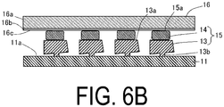
- FIG. 6 is a cross-sectional view illustrating a bonding step according to the first embodiment. Subsequently, as illustrated in FIG. 6(a) , the opposing surface 16c of the support substrate 16 and the upper surface 15a of the semiconductor element 15 are brought into contact with each other. Since the first surface 13a of the semiconductor element layer 13 is inclined as described above, the upper surface 15a of the semiconductor element 15, which is the upper surface of the metal layer 14 formed on the first surface 13a, is also inclined.
- the support substrate 16 is pressed such that the metal layer 14 is pressed into close contact with the support substrate 16, and then heated to, for example, 300°C to perform AuSn bonding.
- the bonding is not limited to AuSn bonding, and various bonding methods using other materials are possible.
- the semiconductor element 15 is displaced so that the entire surface of the upper surface 15a of the semiconductor element 15 abuts against the opposing surface 16c. As a result, a large stress is generated in the connecting portion 13b of the semiconductor element layer 13, and the connecting portion 13b is broken.
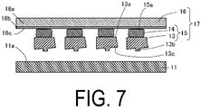
- FIG. 7 is a cross-sectional view illustrating a peeling step according to the first embodiment.
- the underlying substrate 11 and the support substrate 16 are taken out from the substrate bonding apparatus.
- the semiconductor element 15 is bonded onto the support substrate 16, and the connecting portion 13b is broken, so that the underlying substrate 11 can be easily peeled off.
- the connecting portion 13b having the columnar shape is attached to the semiconductor element layer 13. It is conceivable that the connecting portion 13b remains on the underlying substrate 11 side, the semiconductor element 15 side, or both, depending on the condition of the breakage. Thus, after the peeling, the connecting portion 13b remaining in the semiconductor element 15 is removed by polishing or the like.
- the first surface 13a of the semiconductor element layer 13 is parallel to the opposing surface 16c, which is a surface of the support substrate 16.
- the second surface 13c of the semiconductor element layer 13 is inclined with respect to the surface of the support substrate 16 in accordance with the inclination of the first surface 13a of the semiconductor element layer 13.
- the first surface 13a of the semiconductor element layer 13 is considered to be parallel to the surface of the support substrate 16, when the inclination is, for example, less than 0.5°.
- the semiconductor element body 17 of the first embodiment includes the support substrate 16, the first surface 13a, and the second surface 13c located on the opposite side to the first surface 13a, and the first surface 13a side is fixed to the support substrate 16.
- the semiconductor element body 17 includes the semiconductor element layer 13 in which the second surface 13c is inclined with respect to the surface of the support substrate 16.
- the semiconductor element 15 is formed with the upper surface 15a inclined with respect to the growth surface 11a of the underlying substrate 11, when being pressed in the bonding step S3, shearing stress is concentrated on the end portion of the connecting portion 13b having the columnar shape, and the connecting portion 13b is sheared. Accordingly, the semiconductor element 15 can be reliably separated from the underlying substrate 11 by simply applying pressure, without the need to separately apply a force in the vertical direction to the surface of the underlying substrate 11 by ultrasonic waves or the like. As described above, since the semiconductor element 15 can be reliably transferred to the support substrate 16 without applying excessive force to the semiconductor element 15, the yield of the semiconductor element 15 can be improved.
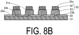
- FIGS. 8A to 8C are cross-sectional views illustrating an element forming step according to a second embodiment.
- an underlying substrate 21 is first prepared.
- a GaN template substrate is used as the underlying substrate 21.
- a crystal plane of a growth surface 21a of the underlying substrate 21 has no off angle.
- a mask 22 is formed in a step similar to that in the first embodiment. The growth surface 21a is exposed through an opening portion 22b of a strip-shaped body 22a of the mask 22.
- a semiconductor element layer 23 which is a crystal growth layer of a nitride semiconductor, is vapor phase grown from the growth surface 20a exposed from the opening portion 22b of the strip-shaped body 22a.
- a semiconductor element 25 is formed on the underlying substrate 21 by etching the mask 22 on the underlying substrate 21.
- the first surface 23a of the semiconductor element layer 23 and an upper surface 25a of the semiconductor element 25 are substantially parallel to the growth surface 21a of the underlying substrate 21.
- the semiconductor element layer 23 has the first surface 23a and a second surface 23c located on the opposite side to the first surface 23a.
- FIG. 9 is a cross-sectional view illustrating a preparing step according to the second embodiment.
- a support substrate 26 for bonding to the semiconductor element 25 is prepared.
- a silicon substrate is used as a base 26a of the support substrate 26.
- the silicon substrate is, for example, an off-angle substrate with a plane direction having an off angle of 0.3° from (111), in other words, the support substrate 26 has an opposing surface 26c caused to face the underlying substrate 21.
- an off-angle substrate in which the opposing surface 26c is a crystal plane having an off angle with respect to the normal line of the opposing surface 26c, can be used.
- a photoresist film having a stripe shape is formed on such an off-angle substrate, and anisotropic etching with potassium hydroxide (KOH) aqueous solution is performed, so that an inclined surface 26d is provided on the base 26a. Furthermore, a metal layer 26b, such as gold, is formed on the silicon substrate by a vapor deposition method or the like.
- the support substrate 26 formed in this manner has the opposing surface 26c having the inclined surface 26d.
- An inclination angle ⁇ of the inclined surface 26d is approximately the same as the off angle.
- the opposing surface 26c of the support substrate 26 is inclined with respect to the underlying substrate 21 by the angle ⁇ .
- the opposing surface 26c is formed for each row of semiconductor elements 25 arranged on the underlying substrate 21. Accordingly, it is preferable that a pitch at which the semiconductor elements 25 are disposed on the underlying substrate 21 and a pitch at which the plurality of the inclined surfaces 26d are formed on the support substrate 26 coincide with each other.
- the semiconductor element 25 is connected to the support substrate 16 by using a substrate bonding apparatus (not illustrated).
- the underlying substrate 21 and the opposing surface 26c are attached to the substrate bonding apparatus such that the growth surface 21a of the underlying substrate 21 and the opposing surface 26c of the support substrate 26 face each other.
- FIGS. 10A and 10B are cross-sectional views illustrating a bonding step according to the second embodiment.
- the opposing surface 26c of the support substrate 26 and the upper surface 25a of the semiconductor element 25 are brought into contact with each other.
- the opposing surface 26c of the support substrate 26 is inclined.
- a portion of the upper surface 25a of the semiconductor element 25 is in contact with the opposing surface 26c.
- the support substrate 26 is pressed such that the upper surface 25a of the semiconductor element 25 is pressed into close contact with the opposing surface 26c of the support substrate 26, and then heated to, for example, 300°C to perform AuSn bonding.
- the semiconductor element 25 is displaced so that the entire surface of the upper surface 25a of the semiconductor element 25 abuts against the opposing surface 26c.
- a large shearing stress is generated in an end portion of the connecting portion 23b of the semiconductor element layer 23, and the connecting portion 23b is broken.
- FIG. 11 is a cross-sectional view illustrating a peeling step according to the second embodiment.
- the semiconductor element 25 is bonded to the opposing surface 26c of the support substrate 26, and the connecting portion 23b is broken, so that the underlying substrate 21 can be easily peeled off.
- the connecting portion 23b having a columnar shape is attached to the semiconductor element layer 23; however, the connecting portion 23b can be removed by polishing or the like.
- the opposing surface 26c of the support substrate 26 is inclined with respect to the growth surface 21a of the underlying substrate 21 or the upper surface 25a of the semiconductor element 25.
- the semiconductor element 25 can be reliably separated from the underlying substrate 21 by simply applying pressure with the substrate bonding apparatus, even without the need to apply a force of ultrasonic waves or the like.
- the semiconductor element 25 can be reliably transferred to the support substrate 26 by simply applying a force smaller than that in the related art to the semiconductor element 25.
- the yield of the semiconductor element 25 can be improved.
- a portion of the opposing surface 26c of the support substrate 26 is inclined.
- the semiconductor element body 27 of the second embodiment includes the support substrate 26, the first surface 23a, and the second surface 23c located on the opposite side to the first surface 23a, and the first surface 23a side is fixed to the support substrate 26.
- the semiconductor element body 27 includes the semiconductor element layer 23 in which the second surface 23c is inclined with respect to the surface of the support substrate 26.
- the underlying substrate used in the element forming step S1 and the formed semiconductor element are similar to those in the second embodiment, and thus descriptions thereof are omitted and the same reference numerals are used.
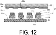
- FIG. 12 is a cross-sectional view illustrating a preparing step according to the third embodiment.
- a support substrate 36 for bonding to a semiconductor element 25 is prepared.
- a silicon substrate is used as a base 36a of the support substrate 36.
- a c-plane substrate having a plane direction of (100) may be used.
- a layer in which, for example, titanium (Ti) is used as an underlying layer and a Au layer is layered thereon is formed on the base 36a.
- a mask having a stripe shape is fabricated on the formed layer, and, for example, AuSn is vapor deposited.
- the support substrate 36 on which an opposing surface 36c of a metal layer 36b having stripe-shaped projections and recesses is formed, is obtained by a vapor deposition lift off method in which the Au layer vapor deposited on the mask is removed together with the mask. It is preferable that a pitch at which the semiconductor elements 25 are disposed on the underlying substrate 21 and a pitch of the stripe-shaped projections and recesses of the support substrate 36 coincide with each other. A stepped portion 36d is formed at the boundary between a projection portion and a recess portion of the opposing surface 36c.
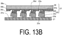
- FIGS. 13A and 13B are cross-sectional views illustrating a bonding step according to the third embodiment.
- the opposing surface 36c of the support substrate 36 and the upper surface 25a of the semiconductor element 25 are brought into contact with each other.
- the opposing surface 36c of the support substrate 36 includes the stepped portion 36d.
- a portion of the upper surface 25a of the semiconductor element 25 is in contact with the opposing surface 36c.
- the support substrate 36 is pressed such that the upper surface 25a is pressed against the support substrate 36, and heated to 300°C to perform AuSn bonding.
- the stepped portion 36d of the opposing surface 36c abuts against the upper surface 25a of the semiconductor element 25, and the semiconductor element 25 is displaced so that the upper surface 25a of the semiconductor element 25 is in proximity to the recess portion of the opposing surface 36c.
- a large shearing stress is generated in the connecting portion 23b of the semiconductor element layer 23, and the connecting portion 23b is broken.
- FIG. 14 is a cross-sectional view illustrating a peeling step according to the third embodiment.
- the semiconductor element 25 is bonded onto the support substrate 36, and the connecting portion 23b is broken, so that the underlying substrate 21 can be easily peeled off.
- the opposing surface 36c becomes flat by the bonding step S3, and the metal layer 36b and the metal layer 24 are integrally formed.
- the first surface 23a of the semiconductor element layer 23 is also fixed, via a metal, to the opposing surface 36c, which is a surface of the support substrate 36.
- the connecting portion 23b having a columnar shape is attached to the semiconductor element layer 23; however, the connecting portion 23b can be removed by polishing or the like.
- the opposing surface 36c of the support substrate 36 includes the stepped portion 36d.
- the semiconductor element 25 can be reliably separated from the underlying substrate 21 by simply applying pressure, even without the need to apply a force, such as ultrasonic waves.
- the semiconductor element 25 can be reliably transferred to the support substrate 36 by simply applying a force smaller than that in the related art to the semiconductor element 25, and hence the yield of the semiconductor element 25 can be improved.
- the first surface 23a of the semiconductor element layer 23 is inclined in accordance with the structure of the stepped portion 36d, with respect to the opposing surface 36c, which is a surface of the support substrate 36.
- the semiconductor element body 37 of the third embodiment includes the support substrate 36, the first surface 23a, and the second surface 23c located on the opposite side to the first surface 23a, and the first surface 23a side is fixed to the support substrate 26.
- the semiconductor element body 37 at least the first surface 23a of the first surface 23a and the second surface 23c is inclined with respect to the surface of the support substrate 36.
- the support substrate 26 can also be configured to have the inclined surface with the simple structure, and similarly to the second embodiment, the semiconductor element body 37 is easily cleaved or the like, which facilitates separation of the semiconductor element body 37 into individual semiconductor elements 25.
Landscapes
- Led Devices (AREA)
- Recrystallisation Techniques (AREA)
Abstract
Description
- The present disclosure relates to a method of manufacturing a semiconductor element, and a semiconductor element body.
- A method of manufacturing a semiconductor element according to a related art is described, for example, in Patent Document 1.
- Patent Document 1:
JP 4638958 B - A method of manufacturing a semiconductor element according to the present disclosure may include an element forming step of forming, on an underlying substrate, a semiconductor element connected to the underlying substrate via a connecting portion and including an upper surface inclined with respect to a growth surface of the underlying substrate, a preparing step of preparing a support substrate including an opposing surface caused to face the underlying substrate, a bonding step of pressing the upper surface of the semiconductor element against the opposing surface of the support substrate and heating the upper surface to bond the upper surface of the semiconductor element to the support substrate, and a peeling step of peeling the semiconductor element from the underlying substrate.
- A method of manufacturing a semiconductor element according to the present disclosure may include an element forming step of forming, on an underlying substrate, a semiconductor element connected to the underlying substrate via a connecting portion, a preparing step of preparing a support substrate including an opposing surface inclined with respect to a growth surface of the underlying substrate when the support substrate is caused to face the underlying substrate, a bonding step of pressing an upper surface of the semiconductor element against the opposing surface of the support substrate and heating the upper surface to bond the upper surface of the semiconductor element to the support substrate, and a peeling step of peeling the semiconductor element from the underlying substrate.
- A method of manufacturing a semiconductor element according to the present disclosure may include an element forming step of forming, on an underlying substrate, a semiconductor element connected to the underlying substrate via a connecting portion, a preparing step of preparing a support substrate including an opposing surface caused to face the underlying substrate, the opposing surface including a stepped portion, a bonding step of pressing an upper surface of the semiconductor element against the opposing surface of the support substrate such that the upper surface of the semiconductor element and the stepped portion of the opposing surface of the support substrate come into contact with each other, and heating the upper surface, to bond the upper surface of the semiconductor element to the support substrate, and a peeling step of peeling the semiconductor element from the underlying substrate.
- A semiconductor element body of the present disclosure may include a support substrate and a semiconductor element layer including a first surface and a second surface located on an opposite side to the first surface, wherein a side with the first surface is fixed to the support substrate, and the second surface is inclined with respect to a surface of the support substrate.
- A semiconductor element body of the present disclosure may include a support substrate including an inclined surface, and a semiconductor element layer including a first surface and a second surface located on an opposite side to the first surface, wherein a side with the first surface is fixed to the inclined surface of the support substrate.
- A semiconductor element body of the present disclosure may include a support substrate and a semiconductor element including a first surface and a second surface located on an opposite side to the first surface, wherein a side with the first surface is fixed to the support substrate, at least the first surface of the first surface and the second surface is inclined with respect to a surface of the support substrate.
- According to the method of manufacturing a semiconductor element of the present disclosure, the yield of the semiconductor element can be increased.
- According to the semiconductor element body of the present disclosure, separation into individual semiconductor elements is facilitated, so that the yield of the semiconductor element can be increased.
-
-
FIG. 1 is a process diagram of a method of manufacturing a semiconductor element according to an embodiment of the present disclosure. -
FIG. 2A is a cross-sectional view illustrating an element forming step according to a first embodiment. -
FIG. 2B is a cross-sectional view illustrating the element forming step according to the first embodiment. -
FIG. 2C is a cross-sectional view illustrating the element forming step according to the first embodiment. -
FIG. 3 is a photograph of a semiconductor element layer formed on an underlying substrate. -
FIG. 4 is a graph illustrating an inclination of an upper surface of a semiconductor element layer. -
FIG. 5 is a cross-sectional view illustrating a preparing step according to the first embodiment. -
FIG. 6A is a cross-sectional view illustrating a bonding step according to the first embodiment. -
FIG. 6B is a cross-sectional view illustrating the bonding step according to the first embodiment. -
FIG. 7 is a cross-sectional view illustrating a peeling step according to the first embodiment. -
FIG. 8A is a cross-sectional view illustrating an element forming step according to a second embodiment. -
FIG. 8B is a cross-sectional view illustrating the element forming step according to the second embodiment. -
FIG. 8C is a cross-sectional view illustrating the element forming step according to the second embodiment. -
FIG. 9 is a cross-sectional view illustrating a preparing step according to the second embodiment. -
FIG. 10A is a cross-sectional view illustrating a bonding step according to the second embodiment. -
FIG. 10B is a cross-sectional view illustrating a bonding step according to the second embodiment. -
FIG. 11 is a cross-sectional view illustrating a peeling step according to the second embodiment. -
FIG. 12 is a cross-sectional view illustrating a preparing step according to a third embodiment. -
FIG. 13A is a cross-sectional view illustrating a bonding step according to the third embodiment. -
FIG. 13B is a cross-sectional view illustrating the bonding step according to the third embodiment. -
FIG. 14 is a cross-sectional view illustrating a peeling step according to the third embodiment. - The objects, features, and advantages of the present invention will become more apparent from the following detailed description and drawings.
- In a semiconductor element and a method of manufacturing the same according to the present disclosure, a mask having a stripe-shaped slit is formed on an underlying substrate made of sapphire, gallium nitride (GaN), or the like. Then, a semiconductor is epitaxially grown from the substrate exposed from the slit, and the formed semiconductor element is transferred to a support substrate.
- In the technology according to the present disclosure, when transferring the grown semiconductor element to the support substrate, after the semiconductor element is bonded to the support substrate, a force in a direction perpendicular to each surface of the underlying substrate and the support substrate is applied to break the connecting portion between the underlying substrate and the semiconductor element. At this time, when a force is applied between the support substrate and the semiconductor element, an electrode of the semiconductor element may be peeled off, and this leads to a high possibility of the semiconductor element not being reliably transferred to the support substrate, for example. Thus, the yield of the semiconductor element may not be improved.
- Embodiments of the present disclosure will be described below with reference to each drawing schematically illustrated.
FIG. 1 is a basic process diagram of a method of manufacturing a semiconductor element according to an embodiment of the present disclosure. A method of manufacturing a semiconductor element according to the present disclosure includes an element forming step S1 of forming a semiconductor element on an underlying substrate, a preparing step S2 of preparing a support substrate, a bonding step S3 of bonding the semiconductor element on the underlying substrate to the support substrate, and a peeling step S4 of peeling the semiconductor element from the underlying substrate. The element forming step S1 and the preparing step S2 need not be performed in this order, and for example, the element forming step S1 and the preparing step S2 may be performed in parallel. -
FIGS. 2A to 2C are cross-sectional views illustrating the element forming step according to the first embodiment. As illustrated inFIG. 2A , first, an underlyingsubstrate 11 is prepared. For example, a GaN template substrate is used as the underlyingsubstrate 11. For example, the underlyingsubstrate 11 is an off-angle substrate, and a normal direction of agrowth surface 11a of the underlying substrate 11 (or the surface perpendicular to a thickness direction of the underlying substrate 11) is inclined by 0.3° from an a axis (< 11-20 >) direction. In the present embodiment, the off angle with respect to the a axis is 0.3°; however, a substrate having an off angle of from 0.1° to 1°, in other words, a substrate in which thegrowth surface 11a of theunderlying substrate 11 is a crystal plane having an off angle with respect to the normal line of thegrowth surface 11a can be used. As theunderlying substrate 11, for example, a GaN substrate cut out from a GaN single crystal ingot so that thegrowth surface 11a of the underlying substrate is in a predetermined plane direction can be used. As theunderlying substrate 11, any nitride semiconductor substrate may be used. Alternatively, an n-type substrate or a p-type substrate in which the nitride semiconductor is doped with impurities may be used. Here, the "nitride semiconductor" is constituted by, for example, AlxGayInzN (0 ≤ x ≤ 1, 0 ≤ y ≤ 1, 0 ≤ z ≤ 1, x + y + z = 1), and this similarly applies to the "nitride semiconductor" described below. As the GaN template substrate, for example, sapphire, Si, or SiC can be used. - Next, a
mask 12 is formed on theunderlying substrate 11. First, by using a plasma chemical vapor deposition (PCVD) method or the like to deposit a silicon oxide (for example, SiO2 or the like), which is the material of the mask, on theunderlying substrate 11, a SiO2 layer of approximately 100 nm is layered on thegrowth surface 11a. Subsequently, the SiO2 layer is patterned by a photolithography method and wet etching using buffered hydrogen fluoride (BHF) to form themask 12 illustrated inFIG. 2A . Themask 12 has a stripe shape in which a plurality of strip-shapedportions 12a are arranged in parallel at a predetermined interval. A width of anopening portion 12b between adjacent strip-shapedportions 12a is, for example, approximately 5 µm. A width of each strip-shapedportion 12a is, for example, from approximately 50 µm to approximately 200 µm. The width of theopening portion 12b is, for example, from approximately 2 µm to approximately 20 µm. - The mask material for forming the
mask 12 may be, in addition to SiO2, a material in which a semiconductor layer does not grow from the mask material by vapor phase epitaxy. As the mask material, for example, an oxide, such as ZrOx, TiOx, or AlOx, which can be patterned, or a transition metal, such as W or Cr can also be used. As the method of layering the mask layer, any method, such as vapor deposition, sputtering, or coating and curing, which are suitable for the mask material, can be used as appropriate. - Subsequently, as illustrated in
FIG. 2B , asemiconductor element layer 13, which is a crystal growth layer of a semiconductor crystal, is vapor phase grown from thegrowth surface 11a exposed from theopening portion 12b. Thesemiconductor element layer 13 of the present disclosure is a nitride semiconductor layer. - As a method of crystal growth, vapor phase epitaxy (VPE) by a chloride transport method using a chloride as a group III raw material, or metal organic chemical vapor deposition (MOCVD) using an organic metal as a group III raw material can be used. A ratio of a raw material gas of a group III element, a ratio of a raw material gas of an impurity, and the like can be changed during the growth step to form the
semiconductor element layer 13 as a multi-layer film that functions as an LED or an LD. - When the grown crystal exceeds the
opening portion 12b of themask 12, the crystal also grows laterally along a maskupper surface 12c. The crystal growth is completed before adjacent portions of thesemiconductor element layer 13 grown from thegrowth surface 11a overlap with each other. In this manner, thesemiconductor element layer 13, which is a nitride semiconductor grown by an epitaxial lateral overgrowth (ELO) method, is obtained. The width of thesemiconductor element layer 13 is, for example, from approximately 50 µm to approximately 200 µm, and the height is from approximately 10 µm to approximately 50 µm. -
FIG. 3 is a photograph of the semiconductor element layer formed on the underlying substrate, and is a top view of the semiconductor element layer formed on the mask by the above-described method.FIG. 4 is a graph showing an inclination of the upper surface of the semiconductor element layer, showing a measurement result of measuring a distance between the upper surface of the semiconductor element layer illustrated inFIG. 3 and a reference surface. A width W of thesemiconductor element layer 13 formed in a strip shape is 35 µm, and in the width direction, the right end side is higher than the left end side, and the height difference between both ends is 150 nm. An inclination angle of afirst surface 13a (upper surface) of thesemiconductor element layer 13 is 0.25°. The off angle of theunderlying substrate 11 used in the growth of thesemiconductor element layer 13 is 0.22°, and the inclination angle of thefirst surface 13a corresponds to the off angle of theunderlying substrate 11. Growing thesemiconductor element layer 13 with the off angle on theunderlying substrate 11 in this manner is advantageous for realizing thesemiconductor element layer 13 of a crystal having excellent quality. Thesemiconductor element layer 13 has thefirst surface 13a and asecond surface 13c located on the opposite side to thefirst surface 13a. - After the
semiconductor element layer 13 is grown, ametal layer 14 is formed on thefirst surface 13a of thesemiconductor element layer 13, as illustrated inFIG. 2B . First, the entire upper surface of theunderlying substrate 11, themask 12, and thesemiconductor element layer 13 is covered with a resist film. Thereafter, an opening portion is provided using a photolithography method so that thefirst surface 13a of thesemiconductor element layer 13 is exposed. Thereafter, for example, a Cr layer and a AuSn layer, which is an alloy of gold and tin, are vapor deposited in order in the opening portion. Thereafter, the unnecessary metal layer is removed together with the resist film by a lift-off method to form themetal layer 14. The thickness of the metal layer is from approximately 1 µm to approximately 5 µm. - After the
metal layer 14 is formed, the underlyingsubstrate 11, themask 12 formed on theunderlying substrate 11, thesemiconductor element layer 13, and themetal layer 14 are immersed in BHF for approximately 10 minutes to remove themask 12. As a result, as illustrated inFIG. 2C , asemiconductor element 15 is formed on theunderlying substrate 11. Thesemiconductor element 15 and theunderlying substrate 11 are connected to each other via, for example, a connectingportion 13b having a columnar shape, which is a portion of thesemiconductor element layer 13 grown in theopening portion 12b of themask 12. Themetal layer 14 can be used as an electrode of thesemiconductor element 15. However, depending on the configuration of thesemiconductor element 15, themetal layer 14 need not necessarily be used as the electrode. Anupper surface 15a of thesemiconductor element 15 is inclined similarly to thefirst surface 13a of thesemiconductor element layer 13. Thesemiconductor element layer 13 has thefirst surface 13a and thesecond surface 13c located on the opposite side to thefirst surface 13a. -
FIG. 5 is a cross-sectional view illustrating a preparing step according to the first embodiment. Subsequently, asupport substrate 16 for connecting to thesemiconductor element 15 is prepared. In thesupport substrate 16, a silicon substrate is used as abase 16a. Ametal layer 16b, such as Au, is formed on one surface of thebase 16a, and a surface of themetal layer 16b is an opposingsurface 16c to face the underlyingsubstrate 11. Themetal layer 16b facilitates bonding of thesemiconductor element 15 to thesupport substrate 16. - Subsequently, the
semiconductor element 15 is connected to thesupport substrate 16 by using a substrate bonding apparatus (not illustrated). First, the underlyingsubstrate 11 and thesupport substrate 16 are attached to the substrate bonding apparatus so that thegrowth surface 11a of theunderlying substrate 11 and the opposingsurface 16c of thesupport substrate 16 are parallel to each other. -
FIG. 6 is a cross-sectional view illustrating a bonding step according to the first embodiment. Subsequently, as illustrated inFIG. 6(a) , the opposingsurface 16c of thesupport substrate 16 and theupper surface 15a of thesemiconductor element 15 are brought into contact with each other. Since thefirst surface 13a of thesemiconductor element layer 13 is inclined as described above, theupper surface 15a of thesemiconductor element 15, which is the upper surface of themetal layer 14 formed on thefirst surface 13a, is also inclined. - Subsequently, as illustrated in
FIG. 6(b) , thesupport substrate 16 is pressed such that themetal layer 14 is pressed into close contact with thesupport substrate 16, and then heated to, for example, 300°C to perform AuSn bonding. However, the bonding is not limited to AuSn bonding, and various bonding methods using other materials are possible. At this time, thesemiconductor element 15 is displaced so that the entire surface of theupper surface 15a of thesemiconductor element 15 abuts against the opposingsurface 16c. As a result, a large stress is generated in the connectingportion 13b of thesemiconductor element layer 13, and the connectingportion 13b is broken. -
FIG. 7 is a cross-sectional view illustrating a peeling step according to the first embodiment. After cooling the substrate bonding apparatus, the underlyingsubstrate 11 and thesupport substrate 16 are taken out from the substrate bonding apparatus. At this time, thesemiconductor element 15 is bonded onto thesupport substrate 16, and the connectingportion 13b is broken, so that theunderlying substrate 11 can be easily peeled off. In the drawing, the connectingportion 13b having the columnar shape is attached to thesemiconductor element layer 13. It is conceivable that the connectingportion 13b remains on theunderlying substrate 11 side, thesemiconductor element 15 side, or both, depending on the condition of the breakage. Thus, after the peeling, the connectingportion 13b remaining in thesemiconductor element 15 is removed by polishing or the like. - In a
semiconductor element body 17 bonded and peeled by the method described above, thefirst surface 13a of thesemiconductor element layer 13 is parallel to the opposingsurface 16c, which is a surface of thesupport substrate 16. On the other hand, thesecond surface 13c of thesemiconductor element layer 13 is inclined with respect to the surface of thesupport substrate 16 in accordance with the inclination of thefirst surface 13a of thesemiconductor element layer 13. Here, thefirst surface 13a of thesemiconductor element layer 13 is considered to be parallel to the surface of thesupport substrate 16, when the inclination is, for example, less than 0.5°. - As described above, the
semiconductor element body 17 of the first embodiment includes thesupport substrate 16, thefirst surface 13a, and thesecond surface 13c located on the opposite side to thefirst surface 13a, and thefirst surface 13a side is fixed to thesupport substrate 16. Thesemiconductor element body 17 includes thesemiconductor element layer 13 in which thesecond surface 13c is inclined with respect to the surface of thesupport substrate 16. As a result, thesemiconductor element layer 13 having excellent quality can be realized by the simple support structure. - As described above, since the
semiconductor element 15 is formed with theupper surface 15a inclined with respect to thegrowth surface 11a of theunderlying substrate 11, when being pressed in the bonding step S3, shearing stress is concentrated on the end portion of the connectingportion 13b having the columnar shape, and the connectingportion 13b is sheared. Accordingly, thesemiconductor element 15 can be reliably separated from the underlyingsubstrate 11 by simply applying pressure, without the need to separately apply a force in the vertical direction to the surface of theunderlying substrate 11 by ultrasonic waves or the like. As described above, since thesemiconductor element 15 can be reliably transferred to thesupport substrate 16 without applying excessive force to thesemiconductor element 15, the yield of thesemiconductor element 15 can be improved. -
FIGS. 8A to 8C are cross-sectional views illustrating an element forming step according to a second embodiment. As illustrated inFIG. 8A , an underlyingsubstrate 21 is first prepared. For example, similar to the first embodiment, a GaN template substrate is used as the underlyingsubstrate 21. However, a crystal plane of agrowth surface 21a of theunderlying substrate 21 has no off angle. Amask 22 is formed in a step similar to that in the first embodiment. Thegrowth surface 21a is exposed through anopening portion 22b of a strip-shapedbody 22a of themask 22. - Subsequently, as illustrated in
FIG. 8B , similar to the first embodiment, asemiconductor element layer 23, which is a crystal growth layer of a nitride semiconductor, is vapor phase grown from the growth surface 20a exposed from theopening portion 22b of the strip-shapedbody 22a. Thereafter, ametal layer 24, such as, for example, a AuSn alloy, is formed on afirst surface 23a of thesemiconductor element layer 23. - Subsequently, as illustrated in
FIG. 8C , asemiconductor element 25 is formed on theunderlying substrate 21 by etching themask 22 on theunderlying substrate 21. Thefirst surface 23a of thesemiconductor element layer 23 and anupper surface 25a of thesemiconductor element 25 are substantially parallel to thegrowth surface 21a of theunderlying substrate 21. Also, in the second embodiment, similar to the first embodiment, thesemiconductor element layer 23 has thefirst surface 23a and asecond surface 23c located on the opposite side to thefirst surface 23a. -
FIG. 9 is a cross-sectional view illustrating a preparing step according to the second embodiment. Subsequently, asupport substrate 26 for bonding to thesemiconductor element 25 is prepared. For example, a silicon substrate is used as abase 26a of thesupport substrate 26. The silicon substrate is, for example, an off-angle substrate with a plane direction having an off angle of 0.3° from (111), in other words, thesupport substrate 26 has an opposingsurface 26c caused to face the underlyingsubstrate 21. As thesupport substrate 26, an off-angle substrate, in which the opposingsurface 26c is a crystal plane having an off angle with respect to the normal line of the opposingsurface 26c, can be used. A photoresist film having a stripe shape is formed on such an off-angle substrate, and anisotropic etching with potassium hydroxide (KOH) aqueous solution is performed, so that aninclined surface 26d is provided on thebase 26a. Furthermore, ametal layer 26b, such as gold, is formed on the silicon substrate by a vapor deposition method or the like. Thesupport substrate 26 formed in this manner has the opposingsurface 26c having theinclined surface 26d. An inclination angle α of theinclined surface 26d is approximately the same as the off angle. - The opposing
surface 26c of thesupport substrate 26 is inclined with respect to theunderlying substrate 21 by the angle α. The opposingsurface 26c is formed for each row ofsemiconductor elements 25 arranged on theunderlying substrate 21. Accordingly, it is preferable that a pitch at which thesemiconductor elements 25 are disposed on theunderlying substrate 21 and a pitch at which the plurality of theinclined surfaces 26d are formed on thesupport substrate 26 coincide with each other. Subsequently, thesemiconductor element 25 is connected to thesupport substrate 16 by using a substrate bonding apparatus (not illustrated). First, the underlyingsubstrate 21 and the opposingsurface 26c are attached to the substrate bonding apparatus such that thegrowth surface 21a of theunderlying substrate 21 and the opposingsurface 26c of thesupport substrate 26 face each other. -
FIGS. 10A and10B are cross-sectional views illustrating a bonding step according to the second embodiment. As illustrated inFIG. 10A , the opposingsurface 26c of thesupport substrate 26 and theupper surface 25a of thesemiconductor element 25 are brought into contact with each other. The opposingsurface 26c of thesupport substrate 26 is inclined. As such, a portion of theupper surface 25a of thesemiconductor element 25 is in contact with the opposingsurface 26c. Subsequently, as illustrated inFIG. 10B , thesupport substrate 26 is pressed such that theupper surface 25a of thesemiconductor element 25 is pressed into close contact with the opposingsurface 26c of thesupport substrate 26, and then heated to, for example, 300°C to perform AuSn bonding. At this time, thesemiconductor element 25 is displaced so that the entire surface of theupper surface 25a of thesemiconductor element 25 abuts against the opposingsurface 26c. As a result, a large shearing stress is generated in an end portion of the connectingportion 23b of thesemiconductor element layer 23, and the connectingportion 23b is broken. -
FIG. 11 is a cross-sectional view illustrating a peeling step according to the second embodiment. When theunderlying substrate 21 and thesupport substrate 26 are taken out from the substrate bonding apparatus after the substrate bonding apparatus is cooled, thesemiconductor element 25 is bonded to the opposingsurface 26c of thesupport substrate 26, and the connectingportion 23b is broken, so that theunderlying substrate 21 can be easily peeled off. In the drawing, for example, the connectingportion 23b having a columnar shape is attached to thesemiconductor element layer 23; however, the connectingportion 23b can be removed by polishing or the like. - As described above, prior to the bonding step S3, the opposing
surface 26c of thesupport substrate 26 is inclined with respect to thegrowth surface 21a of theunderlying substrate 21 or theupper surface 25a of thesemiconductor element 25. Thus, when theupper surface 25a of thesemiconductor element 25 is pressed against the opposingsurface 26c of thesupport substrate 26 in the bonding step S3, shearing stress is concentrated on an end portion of the connectingportion 23b, and the connectingportion 23b is sheared. Accordingly, thesemiconductor element 25 can be reliably separated from the underlyingsubstrate 21 by simply applying pressure with the substrate bonding apparatus, even without the need to apply a force of ultrasonic waves or the like. As described above, thesemiconductor element 25 can be reliably transferred to thesupport substrate 26 by simply applying a force smaller than that in the related art to thesemiconductor element 25. Thus, the yield of thesemiconductor element 25 can be improved. - In a
semiconductor element body 27 bonded and peeled by the method described above, a portion of the opposingsurface 26c of thesupport substrate 26 is inclined. - As described above, the
semiconductor element body 27 of the second embodiment includes thesupport substrate 26, thefirst surface 23a, and thesecond surface 23c located on the opposite side to thefirst surface 23a, and thefirst surface 23a side is fixed to thesupport substrate 26. Thesemiconductor element body 27 includes thesemiconductor element layer 23 in which thesecond surface 23c is inclined with respect to the surface of thesupport substrate 26. As a result, since thesupport substrate 26 also has an inclined surface, thesemiconductor element body 27 is easily cleaved or the like, which facilitates the separation of thesemiconductor element body 27 intoindividual semiconductor elements 25. - In a third embodiment, the underlying substrate used in the element forming step S1 and the formed semiconductor element are similar to those in the second embodiment, and thus descriptions thereof are omitted and the same reference numerals are used.
-
FIG. 12 is a cross-sectional view illustrating a preparing step according to the third embodiment. Asupport substrate 36 for bonding to asemiconductor element 25 is prepared. For example, a silicon substrate is used as abase 36a of thesupport substrate 36. As thebase 36a, for example, a c-plane substrate having a plane direction of (100) may be used. First, a layer in which, for example, titanium (Ti) is used as an underlying layer and a Au layer is layered thereon is formed on thebase 36a. A mask having a stripe shape is fabricated on the formed layer, and, for example, AuSn is vapor deposited. Thereafter, thesupport substrate 36, on which an opposingsurface 36c of ametal layer 36b having stripe-shaped projections and recesses is formed, is obtained by a vapor deposition lift off method in which the Au layer vapor deposited on the mask is removed together with the mask. It is preferable that a pitch at which thesemiconductor elements 25 are disposed on theunderlying substrate 21 and a pitch of the stripe-shaped projections and recesses of thesupport substrate 36 coincide with each other. A steppedportion 36d is formed at the boundary between a projection portion and a recess portion of the opposingsurface 36c. - The
semiconductor element 25 and thesupport substrate 36 are bonded using a substrate bonding apparatus (not illustrated).FIGS. 13A and13B are cross-sectional views illustrating a bonding step according to the third embodiment. As illustrated inFIG. 13A , the opposingsurface 36c of thesupport substrate 36 and theupper surface 25a of thesemiconductor element 25 are brought into contact with each other. The opposingsurface 36c of thesupport substrate 36 includes the steppedportion 36d. Thus, a portion of theupper surface 25a of thesemiconductor element 25 is in contact with the opposingsurface 36c. Subsequently, as illustrated inFIG. 13B , thesupport substrate 36 is pressed such that theupper surface 25a is pressed against thesupport substrate 36, and heated to 300°C to perform AuSn bonding. At this time, the steppedportion 36d of the opposingsurface 36c abuts against theupper surface 25a of thesemiconductor element 25, and thesemiconductor element 25 is displaced so that theupper surface 25a of thesemiconductor element 25 is in proximity to the recess portion of the opposingsurface 36c. As a result, a large shearing stress is generated in the connectingportion 23b of thesemiconductor element layer 23, and the connectingportion 23b is broken. -
FIG. 14 is a cross-sectional view illustrating a peeling step according to the third embodiment. When theunderlying substrate 21 and thesupport substrate 36 are taken out from the substrate bonding apparatus after the substrate bonding apparatus is cooled, thesemiconductor element 25 is bonded onto thesupport substrate 36, and the connectingportion 23b is broken, so that theunderlying substrate 21 can be easily peeled off. At this time, the opposingsurface 36c becomes flat by the bonding step S3, and themetal layer 36b and themetal layer 24 are integrally formed. In other words, thefirst surface 23a of thesemiconductor element layer 23 is also fixed, via a metal, to the opposingsurface 36c, which is a surface of thesupport substrate 36. In the drawing, for example, the connectingportion 23b having a columnar shape is attached to thesemiconductor element layer 23; however, the connectingportion 23b can be removed by polishing or the like. - As described above, the opposing
surface 36c of thesupport substrate 36 includes the steppedportion 36d. Thus, when theupper surface 25a of thesemiconductor element 25 is pressed against the opposingsurface 36c in the bonding step S3, shearing stress is concentrated on the end portion of the connectingportion 23b on theunderlying substrate 21 side, and the connectingportion 23b is sheared. Accordingly, thesemiconductor element 25 can be reliably separated from the underlyingsubstrate 21 by simply applying pressure, even without the need to apply a force, such as ultrasonic waves. As described above, thesemiconductor element 25 can be reliably transferred to thesupport substrate 36 by simply applying a force smaller than that in the related art to thesemiconductor element 25, and hence the yield of thesemiconductor element 25 can be improved. - In a
semiconductor element body 37 bonded and peeled by the method described above, thefirst surface 23a of thesemiconductor element layer 23 is inclined in accordance with the structure of the steppedportion 36d, with respect to the opposingsurface 36c, which is a surface of thesupport substrate 36. - As described above, the
semiconductor element body 37 of the third embodiment includes thesupport substrate 36, thefirst surface 23a, and thesecond surface 23c located on the opposite side to thefirst surface 23a, and thefirst surface 23a side is fixed to thesupport substrate 26. In thesemiconductor element body 37, at least thefirst surface 23a of thefirst surface 23a and thesecond surface 23c is inclined with respect to the surface of thesupport substrate 36. As a result, thesupport substrate 26 can also be configured to have the inclined surface with the simple structure, and similarly to the second embodiment, thesemiconductor element body 37 is easily cleaved or the like, which facilitates separation of thesemiconductor element body 37 intoindividual semiconductor elements 25. - The present disclosure has been described in detail above. However, the present disclosure is not limited to the embodiments described above, and various modifications or improvements can be made without departing from the essential spirit of the present disclosure. Accordingly, the foregoing embodiment is merely illustrative in all respects, and the scope of the present invention is as set forth in the claims and is in no way limited by the specification. Furthermore, any variations or modifications that fall within the scope of the claims are also within the scope of the present invention.
-
- S1 Element forming step
- S2 Preparing step
- S3 Bonding step
- S4 Peeling step
- 11, 21 Underlying substrate
- 13. 23 Semiconductor element layer
- 13a, 23a First surface
- 13b, 23b Connecting portion
- 13c. 23c Second surface
- 14, 24, 16b, 26b, 36b Metal layer
- 15, 25 Semiconductor element
- 15a, 25a Upper surface
- 16, 26, 36 Support substrate
- 16c, 26c, 36c Opposing surface
- 17. 27, 37 Semiconductor element body
Claims (10)
- A method of manufacturing a semiconductor element comprising:an element forming step of forming, on an underlying substrate, a semiconductor element connected to the underlying substrate via a connecting portion and comprising an upper surface inclined with respect to a growth surface of the underlying substrate;a preparing step of preparing a support substrate comprising an opposing surface caused to face the underlying substrate;a bonding step of pressing the upper surface of the semiconductor element against the opposing surface of the support substrate and heating the upper surface to bond the upper surface of the semiconductor element to the support substrate; anda peeling step of peeling the semiconductor element from the underlying sub strate.
- The method of manufacturing a semiconductor element according to claim 1, wherein
the growth surface of the underlying substrate is a crystal plane with an off angle with respect to a normal line of the growth surface. - A method of manufacturing a semiconductor element comprising:an element forming step of forming, on an underlying substrate, a semiconductor element connected to the underlying substrate via a connecting portion;a preparing step of preparing a support substrate comprising an opposing surface inclined with respect to a growth surface of the underlying substrate when the support substrate is caused to face the underlying substrate;a bonding step of pressing an upper surface of the semiconductor element against the opposing surface of the support substrate and heating the upper surface to bond the upper surface of the semiconductor element to the support substrate; anda peeling step of peeling the semiconductor element from the underlying sub strate.
- The method of manufacturing a semiconductor element according to claim 3, wherein
the opposing surface of the support substrate is a crystal plane with an off angle with respect to a normal line of the opposing surface. - A method of manufacturing a semiconductor element comprising the steps of:an element forming step of forming, on an underlying substrate, a semiconductor element connected to the underlying substrate via a connecting portion;a preparing step of preparing a support substrate comprising an opposing surface is caused to face the underlying substrate, the opposing surface comprising a stepped portion;a bonding step of pressing an upper surface of the semiconductor element against the opposing surface of the support substrate such that the upper surface of the semiconductor element and the stepped portion of the opposing surface of the support substrate come into contact with each other, and heating the upper surface, to bond the upper surface of the semiconductor element to the support substrate; anda peeling step of peeling the semiconductor element from the underlying sub strate.
- The method of manufacturing a semiconductor element according to claim 5, wherein
in the bonding step, a portion of the upper surface of the semiconductor element is in contact with the stepped portion of the opposing surface of the support substrate. - A semiconductor element body comprising:a support substrate; anda semiconductor element layer comprising a first surface and a second surface located on an opposite side to the first surface, wherein a side with the first surface is fixed to the support substrate, and the second surface is inclined with respect to a surface of the support substrate.
- A semiconductor element body comprising:a support substrate comprising an inclined surface; anda semiconductor element layer comprising a first surface and a second surface located on an opposite side to the first surface, whereina side with the first surface is fixed to the inclined surface of the support sub strate.
- A semiconductor element body comprising:a support substrate; anda semiconductor element layer comprising a first surface and a second surface located on an opposite side to the first surface, whereina side with the first surface is fixed to the support substrate, andat least the first surface of the first surface and the second surface is inclined with respect to a surface of the support substrate.
- The semiconductor element body according to claim 8 or 9, wherein
the first surface of the semiconductor element layer is fixed to the surface of the support substrate via a metal.
Applications Claiming Priority (2)
| Application Number | Priority Date | Filing Date | Title |
|---|---|---|---|
| JP2019036097 | 2019-02-28 | ||
| PCT/JP2020/008399 WO2020175684A1 (en) | 2019-02-28 | 2020-02-28 | Method for manufacturing semiconductor element and semiconductor element body |
Publications (3)
| Publication Number | Publication Date |
|---|---|
| EP3933886A1 true EP3933886A1 (en) | 2022-01-05 |
| EP3933886A4 EP3933886A4 (en) | 2022-09-28 |
| EP3933886B1 EP3933886B1 (en) | 2026-03-18 |
Family
ID=72239807
Family Applications (1)
| Application Number | Title | Priority Date | Filing Date |
|---|---|---|---|
| EP20762528.6A Active EP3933886B1 (en) | 2019-02-28 | 2020-02-28 | Method for manufacturing semiconductor element and semiconductor element body |
Country Status (5)
| Country | Link |
|---|---|
| US (1) | US12132142B2 (en) |
| EP (1) | EP3933886B1 (en) |
| JP (1) | JP7267394B2 (en) |
| CN (2) | CN113490995B (en) |
| WO (1) | WO2020175684A1 (en) |
Families Citing this family (1)
| Publication number | Priority date | Publication date | Assignee | Title |
|---|---|---|---|---|
| JP7854514B2 (en) * | 2022-12-05 | 2026-05-01 | 京セラ株式会社 | Method and apparatus for manufacturing semiconductor devices |
Family Cites Families (8)
| Publication number | Priority date | Publication date | Assignee | Title |
|---|---|---|---|---|
| JPS4638958B1 (en) | 1962-03-20 | 1971-11-16 | ||
| JP4731180B2 (en) * | 2005-02-21 | 2011-07-20 | 三洋電機株式会社 | Nitride semiconductor device manufacturing method |
| JP2007096114A (en) | 2005-09-29 | 2007-04-12 | Sanyo Electric Co Ltd | Semiconductor light emitting element and manufacturing method thereof |
| JP5070247B2 (en) * | 2009-06-23 | 2012-11-07 | 株式会社沖データ | Semiconductor device manufacturing method and semiconductor device |
| JP4638958B1 (en) * | 2009-08-20 | 2011-02-23 | 株式会社パウデック | Manufacturing method of semiconductor device |
| JP5466479B2 (en) * | 2009-10-27 | 2014-04-09 | スタンレー電気株式会社 | Manufacturing method of semiconductor device |
| WO2015160909A1 (en) * | 2014-04-16 | 2015-10-22 | Yale University | Method of obtaining planar semipolar gallium nitride surfaces |
| US20230260943A1 (en) * | 2022-02-17 | 2023-08-17 | Micron Technology, Inc. | Semiconductor die assemblies with flexible interconnects and associated methods and systems |
-
2020
- 2020-02-28 CN CN202080016757.3A patent/CN113490995B/en active Active
- 2020-02-28 CN CN202510136611.7A patent/CN120015705A/en active Pending
- 2020-02-28 JP JP2021502652A patent/JP7267394B2/en active Active
- 2020-02-28 US US17/434,253 patent/US12132142B2/en active Active
- 2020-02-28 EP EP20762528.6A patent/EP3933886B1/en active Active
- 2020-02-28 WO PCT/JP2020/008399 patent/WO2020175684A1/en not_active Ceased
Also Published As
| Publication number | Publication date |
|---|---|
| WO2020175684A1 (en) | 2020-09-03 |
| JP7267394B2 (en) | 2023-05-01 |
| US20220140179A1 (en) | 2022-05-05 |
| CN113490995B (en) | 2025-02-25 |
| CN113490995A (en) | 2021-10-08 |
| JPWO2020175684A1 (en) | 2020-09-03 |
| CN120015705A (en) | 2025-05-16 |
| US12132142B2 (en) | 2024-10-29 |
| EP3933886B1 (en) | 2026-03-18 |
| EP3933886A4 (en) | 2022-09-28 |
Similar Documents
| Publication | Publication Date | Title |
|---|---|---|
| CN105702562B (en) | Preparation method of group III nitride substrate using chemical lift-off method | |
| US20110124139A1 (en) | Method for manufacturing free-standing substrate and free-standing light-emitting device | |
| EP4300605A1 (en) | Semiconductor substrate, method for producing same, apparatus for producing same, and template substrate | |
| JP7314269B2 (en) | LAMINATED PRODUCT AND METHOD OF MANUFACTURING LAMINATED BODY | |
| US9318653B2 (en) | Luminescent device and manufacturing method for luminescent device and semiconductor device | |
| JP2008143772A (en) | Method for producing group III nitride crystal | |
| JP7645319B2 (en) | Semiconductor Device | |
| JP5765367B2 (en) | GaN crystal | |
| EP3933886B1 (en) | Method for manufacturing semiconductor element and semiconductor element body | |
| JP7779906B2 (en) | Semiconductor substrate, manufacturing method and manufacturing apparatus thereof, GaN-based crystal, semiconductor device, electronic device | |
| US12550674B2 (en) | Method for manufacturing semiconductor element, semiconductor element body, and semiconductor element substrate | |
| KR101259999B1 (en) | Semiconductor substrate and method of fabricating the same | |
| US12065760B2 (en) | Method of manufacturing semiconductor element, semiconductor element, and substrate | |
| KR100638351B1 (en) | semiconductor substrate and the manufacturing method of the same | |
| EP4362115A1 (en) | Semiconductor device manufacturing method and manufacturing device, semiconductor device and electronic device | |
| KR100813561B1 (en) | Semiconductor substrate and manufacturing method thereof | |
| US20220376132A1 (en) | Method for manufacturing semiconductor element | |
| CN117374171A (en) | Methods of fabricating semiconductor structures |
Legal Events
| Date | Code | Title | Description |
|---|---|---|---|
| STAA | Information on the status of an ep patent application or granted ep patent |
Free format text: STATUS: THE INTERNATIONAL PUBLICATION HAS BEEN MADE |
|
| PUAI | Public reference made under article 153(3) epc to a published international application that has entered the european phase |
Free format text: ORIGINAL CODE: 0009012 |
|
| STAA | Information on the status of an ep patent application or granted ep patent |
Free format text: STATUS: REQUEST FOR EXAMINATION WAS MADE |
|
| 17P | Request for examination filed |
Effective date: 20210827 |
|
| AK | Designated contracting states |
Kind code of ref document: A1 Designated state(s): AL AT BE BG CH CY CZ DE DK EE ES FI FR GB GR HR HU IE IS IT LI LT LU LV MC MK MT NL NO PL PT RO RS SE SI SK SM TR |
|
| DAV | Request for validation of the european patent (deleted) | ||
| DAX | Request for extension of the european patent (deleted) | ||
| A4 | Supplementary search report drawn up and despatched |
Effective date: 20220825 |
|
| RIC1 | Information provided on ipc code assigned before grant |
Ipc: H01L 21/78 20060101ALI20220819BHEP Ipc: H01L 21/205 20060101ALI20220819BHEP Ipc: H01L 21/20 20060101ALI20220819BHEP Ipc: H01L 21/02 20060101AFI20220819BHEP |
|
| P01 | Opt-out of the competence of the unified patent court (upc) registered |
Effective date: 20230505 |
|
| REG | Reference to a national code |
Ref country code: DE Ref legal event code: R079 Free format text: PREVIOUS MAIN CLASS: H01L0021020000 Ipc: H01L0021780000 Ref document number: 602020068832 Country of ref document: DE |
|
| GRAP | Despatch of communication of intention to grant a patent |
Free format text: ORIGINAL CODE: EPIDOSNIGR1 |
|
| STAA | Information on the status of an ep patent application or granted ep patent |
Free format text: STATUS: GRANT OF PATENT IS INTENDED |
|
| RIC1 | Information provided on ipc code assigned before grant |
Ipc: H01L 21/78 20060101AFI20250917BHEP Ipc: H01L 21/02 20060101ALI20250917BHEP Ipc: H01L 23/48 20060101ALI20250917BHEP |
|
| INTG | Intention to grant announced |
Effective date: 20251015 |
|
| GRAS | Grant fee paid |
Free format text: ORIGINAL CODE: EPIDOSNIGR3 |
|
| GRAA | (expected) grant |
Free format text: ORIGINAL CODE: 0009210 |
|
| STAA | Information on the status of an ep patent application or granted ep patent |
Free format text: STATUS: THE PATENT HAS BEEN GRANTED |
|
| AK | Designated contracting states |
Kind code of ref document: B1 Designated state(s): AL AT BE BG CH CY CZ DE DK EE ES FI FR GB GR HR HU IE IS IT LI LT LU LV MC MK MT NL NO PL PT RO RS SE SI SK SM TR |
|
| REG | Reference to a national code |
Ref country code: CH Ref legal event code: F10 Free format text: ST27 STATUS EVENT CODE: U-0-0-F10-F00 (AS PROVIDED BY THE NATIONAL OFFICE) Effective date: 20260318 Ref country code: GB Ref legal event code: FG4D |
|
| REG | Reference to a national code |
Ref country code: IE Ref legal event code: FG4D |
|
| REG | Reference to a national code |
Ref country code: DE Ref legal event code: R096 Ref document number: 602020068832 Country of ref document: DE |