EP3933839A1 - Memory block and memory - Google Patents
Memory block and memory Download PDFInfo
- Publication number
- EP3933839A1 EP3933839A1 EP21773437.5A EP21773437A EP3933839A1 EP 3933839 A1 EP3933839 A1 EP 3933839A1 EP 21773437 A EP21773437 A EP 21773437A EP 3933839 A1 EP3933839 A1 EP 3933839A1
- Authority
- EP
- European Patent Office
- Prior art keywords
- unit
- signal line
- data signal
- bank
- storage arrays
- Prior art date
- Legal status (The legal status is an assumption and is not a legal conclusion. Google has not performed a legal analysis and makes no representation as to the accuracy of the status listed.)
- Granted
Links
Images



Classifications
-
- G—PHYSICS
- G11—INFORMATION STORAGE
- G11C—STATIC STORES
- G11C11/00—Digital stores characterised by the use of particular electric or magnetic storage elements; Storage elements therefor
- G11C11/21—Digital stores characterised by the use of particular electric or magnetic storage elements; Storage elements therefor using electric elements
- G11C11/34—Digital stores characterised by the use of particular electric or magnetic storage elements; Storage elements therefor using electric elements using semiconductor devices
- G11C11/40—Digital stores characterised by the use of particular electric or magnetic storage elements; Storage elements therefor using electric elements using semiconductor devices using transistors
- G11C11/401—Digital stores characterised by the use of particular electric or magnetic storage elements; Storage elements therefor using electric elements using semiconductor devices using transistors forming cells needing refreshing or charge regeneration, i.e. dynamic cells
- G11C11/4063—Auxiliary circuits, e.g. for addressing, decoding, driving, writing, sensing or timing
- G11C11/407—Auxiliary circuits, e.g. for addressing, decoding, driving, writing, sensing or timing for memory cells of the field-effect type
- G11C11/409—Read-write [R-W] circuits
- G11C11/4097—Bit-line organisation, e.g. bit-line layout, folded bit lines
-
- G—PHYSICS
- G11—INFORMATION STORAGE
- G11C—STATIC STORES
- G11C11/00—Digital stores characterised by the use of particular electric or magnetic storage elements; Storage elements therefor
- G11C11/21—Digital stores characterised by the use of particular electric or magnetic storage elements; Storage elements therefor using electric elements
- G11C11/34—Digital stores characterised by the use of particular electric or magnetic storage elements; Storage elements therefor using electric elements using semiconductor devices
- G11C11/40—Digital stores characterised by the use of particular electric or magnetic storage elements; Storage elements therefor using electric elements using semiconductor devices using transistors
- G11C11/401—Digital stores characterised by the use of particular electric or magnetic storage elements; Storage elements therefor using electric elements using semiconductor devices using transistors forming cells needing refreshing or charge regeneration, i.e. dynamic cells
- G11C11/4063—Auxiliary circuits, e.g. for addressing, decoding, driving, writing, sensing or timing
- G11C11/407—Auxiliary circuits, e.g. for addressing, decoding, driving, writing, sensing or timing for memory cells of the field-effect type
- G11C11/408—Address circuits
- G11C11/4085—Word line control circuits, e.g. word line drivers, - boosters, - pull-up, - pull-down, - precharge
-
- G—PHYSICS
- G11—INFORMATION STORAGE
- G11C—STATIC STORES
- G11C11/00—Digital stores characterised by the use of particular electric or magnetic storage elements; Storage elements therefor
- G11C11/21—Digital stores characterised by the use of particular electric or magnetic storage elements; Storage elements therefor using electric elements
- G11C11/34—Digital stores characterised by the use of particular electric or magnetic storage elements; Storage elements therefor using electric elements using semiconductor devices
- G11C11/40—Digital stores characterised by the use of particular electric or magnetic storage elements; Storage elements therefor using electric elements using semiconductor devices using transistors
- G11C11/401—Digital stores characterised by the use of particular electric or magnetic storage elements; Storage elements therefor using electric elements using semiconductor devices using transistors forming cells needing refreshing or charge regeneration, i.e. dynamic cells
- G11C11/402—Digital stores characterised by the use of particular electric or magnetic storage elements; Storage elements therefor using electric elements using semiconductor devices using transistors forming cells needing refreshing or charge regeneration, i.e. dynamic cells with charge regeneration individual to each memory cell, i.e. internal refresh
- G11C11/4023—Digital stores characterised by the use of particular electric or magnetic storage elements; Storage elements therefor using electric elements using semiconductor devices using transistors forming cells needing refreshing or charge regeneration, i.e. dynamic cells with charge regeneration individual to each memory cell, i.e. internal refresh using field effect transistors
-
- G—PHYSICS
- G11—INFORMATION STORAGE
- G11C—STATIC STORES
- G11C11/00—Digital stores characterised by the use of particular electric or magnetic storage elements; Storage elements therefor
- G11C11/21—Digital stores characterised by the use of particular electric or magnetic storage elements; Storage elements therefor using electric elements
- G11C11/34—Digital stores characterised by the use of particular electric or magnetic storage elements; Storage elements therefor using electric elements using semiconductor devices
- G11C11/40—Digital stores characterised by the use of particular electric or magnetic storage elements; Storage elements therefor using electric elements using semiconductor devices using transistors
- G11C11/401—Digital stores characterised by the use of particular electric or magnetic storage elements; Storage elements therefor using electric elements using semiconductor devices using transistors forming cells needing refreshing or charge regeneration, i.e. dynamic cells
- G11C11/4063—Auxiliary circuits, e.g. for addressing, decoding, driving, writing, sensing or timing
- G11C11/407—Auxiliary circuits, e.g. for addressing, decoding, driving, writing, sensing or timing for memory cells of the field-effect type
- G11C11/408—Address circuits
- G11C11/4087—Address decoders, e.g. bit - or word line decoders; Multiple line decoders
-
- G—PHYSICS
- G11—INFORMATION STORAGE
- G11C—STATIC STORES
- G11C11/00—Digital stores characterised by the use of particular electric or magnetic storage elements; Storage elements therefor
- G11C11/21—Digital stores characterised by the use of particular electric or magnetic storage elements; Storage elements therefor using electric elements
- G11C11/34—Digital stores characterised by the use of particular electric or magnetic storage elements; Storage elements therefor using electric elements using semiconductor devices
- G11C11/40—Digital stores characterised by the use of particular electric or magnetic storage elements; Storage elements therefor using electric elements using semiconductor devices using transistors
- G11C11/401—Digital stores characterised by the use of particular electric or magnetic storage elements; Storage elements therefor using electric elements using semiconductor devices using transistors forming cells needing refreshing or charge regeneration, i.e. dynamic cells
- G11C11/4063—Auxiliary circuits, e.g. for addressing, decoding, driving, writing, sensing or timing
- G11C11/407—Auxiliary circuits, e.g. for addressing, decoding, driving, writing, sensing or timing for memory cells of the field-effect type
- G11C11/409—Read-write [R-W] circuits
-
- G—PHYSICS
- G11—INFORMATION STORAGE
- G11C—STATIC STORES
- G11C5/00—Details of stores covered by group G11C11/00
- G11C5/06—Arrangements for interconnecting storage elements electrically, e.g. by wiring
- G11C5/10—Arrangements for interconnecting storage elements electrically, e.g. by wiring for interconnecting capacitors
-
- G—PHYSICS
- G11—INFORMATION STORAGE
- G11C—STATIC STORES
- G11C11/00—Digital stores characterised by the use of particular electric or magnetic storage elements; Storage elements therefor
- G11C11/21—Digital stores characterised by the use of particular electric or magnetic storage elements; Storage elements therefor using electric elements
- G11C11/34—Digital stores characterised by the use of particular electric or magnetic storage elements; Storage elements therefor using electric elements using semiconductor devices
- G11C11/40—Digital stores characterised by the use of particular electric or magnetic storage elements; Storage elements therefor using electric elements using semiconductor devices using transistors
- G11C11/401—Digital stores characterised by the use of particular electric or magnetic storage elements; Storage elements therefor using electric elements using semiconductor devices using transistors forming cells needing refreshing or charge regeneration, i.e. dynamic cells
- G11C11/4063—Auxiliary circuits, e.g. for addressing, decoding, driving, writing, sensing or timing
- G11C11/407—Auxiliary circuits, e.g. for addressing, decoding, driving, writing, sensing or timing for memory cells of the field-effect type
- G11C11/409—Read-write [R-W] circuits
- G11C11/4091—Sense or sense/refresh amplifiers, or associated sense circuitry, e.g. for coupled bit-line precharging, equalising or isolating
-
- G—PHYSICS
- G11—INFORMATION STORAGE
- G11C—STATIC STORES
- G11C2207/00—Indexing scheme relating to arrangements for writing information into, or reading information out from, a digital store
- G11C2207/005—Transfer gates, i.e. gates coupling the sense amplifier output to data lines, I/O lines or global bit lines
-
- Y—GENERAL TAGGING OF NEW TECHNOLOGICAL DEVELOPMENTS; GENERAL TAGGING OF CROSS-SECTIONAL TECHNOLOGIES SPANNING OVER SEVERAL SECTIONS OF THE IPC; TECHNICAL SUBJECTS COVERED BY FORMER USPC CROSS-REFERENCE ART COLLECTIONS [XRACs] AND DIGESTS
- Y02—TECHNOLOGIES OR APPLICATIONS FOR MITIGATION OR ADAPTATION AGAINST CLIMATE CHANGE
- Y02D—CLIMATE CHANGE MITIGATION TECHNOLOGIES IN INFORMATION AND COMMUNICATION TECHNOLOGIES [ICT], I.E. INFORMATION AND COMMUNICATION TECHNOLOGIES AIMING AT THE REDUCTION OF THEIR OWN ENERGY USE
- Y02D10/00—Energy efficient computing, e.g. low power processors, power management or thermal management
Definitions
- Embodiments of the present application relate to the technical field of semiconductors, and more particularly, to a memory bank and a memory.
- DRAM Dynamic Random Access Memory
- Each storage unit usually includes a capacitor and a transistor.
- a gate of the transistor is connected with a word line, a drain is connected with a bit line, and a source is connected with the capacitor.
- a voltage signal on the word line can control the transistor to be turned on or turned off to further read data information stored in the capacitor through the bit line or write data information in the capacitor for storage through the bit line.
- DRAM includes Double Data Rate (DDR) DRAM, Graphics Double Data Rate (GDDR) DRAM, and Low Power Double Data Rate (LPDDR) DRAM.
- DDR Double Data Rate
- GDDR Graphics Double Data Rate
- LPDDR Low Power Double Data Rate
- the embodiments of the disclosure provide a bank and a memory as a solution to the technical problem.
- the embodiments of the disclosure provide a bank, which includes at least one storage module, each storage module including a read-write control circuit, a column decoding circuit and a plurality of storage arrays arranged along a first direction which are divided into at least one first unit and at least one second unit.
- the first decoding selective signal line is electrically connected to the column decoding circuit and the storage arrays in the first unit and the second decoding selective signal line is electrically connected to the column decoding circuit and the storage arrays in the second unit.
- the first data signal line is electrically connected to the read-write control circuit and the storage arrays in the first unit and the second data signal line is electrically connected to the read-write control circuit and the storage arrays in the second unit.
- first unit and one second unit are provided in which both the first unit and the second unit are a high address unit or both are a low address unit.
- first data signal line is electrically connected to all storage arrays in the first unit and the second data signal line is electrically connected to all storage arrays in the second unit.
- the number of the storage arrays in the first unit is the same as that of the storage arrays in the second unit.
- both the first data signal line and the second data signal line are electrically connected to the read-write control circuit.
- the bank includes a shift switch module, the shift switch module being configured to electrically connect either the first data signal line or the second data signal line to the read-write control circuit.
- the shift switch module may include a control unit and a switch unit where the control unit generates a control signal based on a row decoding signal received by the control unit and, based on the control signal, the switch unit is configured to connect either the read-write control circuit with the first data signal line or the read-write control circuit with the second data signal line.
- the switch unit includes a first switch and a second switch where the first switch is connects the first data signal line and the read-write control circuit and the second switch is connects the second data signal line and the read-write control circuit.
- the bank includes two storage modules with one storage module being a high address module and the other storage module being a low address module.
- the bank includes a positioning control module where the positioning control module is configured to control a row decoding signal generated by a row decoding circuit so that the row decoding circuit simultaneously positions and selects the first unit of the high address module and the second unit of the low address module or simultaneously positions and selects the second unit of the high address module and the first unit of the low address module.
- the first unit includes a first high address unit and a first low address unit and the second unit includes a second high address unit and a second low address unit.
- the first data signal line is electrically connected to the read-write control circuit and the storage arrays in the first high address unit;
- first data signal line and the third data signal line are the same bus; and the second data signal line and the fourth data signal line are the same bus.
- first low address unit is adjacent to the second high address unit; or the first low address unit and the second high address unit are spaced apart by the second low address unit.
- the bank includes two storage modules.
- the column decoding circuit includes: a first column decoding circuit and a second column decoding circuit, where the first decoding selective signal line is electrically connected to the first column decoding circuit and the storage arrays in the first unit, and the second decoding selective signal line is electrically connected to the second column decoding circuit and the storage arrays in the second unit.
- first column decoding circuit and the second column decoding circuit are respectively located on the opposing sides of the plurality of storage arrays.
- the first decoding selective signal line and the second decoding selective signal line are electrically connected to the same column decoding circuit.
- the bank includes: a row decoding circuit, used to send a row decoding signal to position and select either the first unit or the second unit.
- the embodiments of the application further provide memory including the bank of the aforementioned embodiment.
- the embodiments of the application provide the bank with an excellent structural performance, which includes a column decoding circuit that positions and selects storage arrays of the first unit and the first decoding selective signal line, a column decoding circuit that positions and selects storage arrays of the second unit and the second decoding selective signal line, a first data signal line for implementing data transmission between the storage arrays in the first unit and a read-write control circuit, and a second data signal line for implementing data transmission between the storage arrays in the second unit and the read-write control circuit.
- a single read-write operation only the first decoding selective signal line or the second decoding selective signal line is enabled.
- the first decoding selective signal line is only electrically connected to part of the storage arrays, i.e., having electrical contacts
- the second decoding selective signal line is only electrically connected to part of the storage arrays
- the electric contacts in the single read-write operation are reduced and the parasitic resistance and parasitic capacitance of the bank are also reduced, thus reducing a power consumption of the bank.
- the first data signal line and the second data signal line for the data transmission are both electrically connected to part of the storage arrays, such that the electric contacts in the single read-write operation are reduced and the parasitic resistance and parasitic capacitance of the bank are also reduced, thus reducing the power consumption of the bank.
- the bank further includes a shift switch module, where the shift switch module is configured to shift either the first data signal line or the second data signal line to electrically connect to the read-write control circuit. Therefore, when the first data signal line transmits a data signal, the second data signal line is completely disconnected from the circuit, to avoid the problem of heat loss resulting from the second data signal line, further reducing the power consumption of the bank; and likewise, when the second data signal line transmits a data signal, the first data signal line is completely disconnected from the circuit, to avoid the problem of heat loss resulting from the first data signal line, further reducing the power consumption of the bank.
- the first unit includes a first high address unit and a first low address unit
- the second unit includes a second high address unit and a second low address unit. Therefore, high data and low data can be acquired in the same unit, and only one unit is selected in each time of row decoding. This way, the bank is able to save more electricity, further reducing the power consumption of the bank.
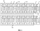
- FIG. 1 is a structural schematic diagram of a DARM.
- the DRAM is composed of multiple banks 10 (also referred to as memory banks).
- Each bank 10 includes several storage arrays.
- Each storage array includes a memory array 11 and a Sense Amplifier (SA) array 12.
- SA Sense Amplifier
- the DRAM regardless of whether the DDR (such as DDR2/3/4) series or the LPDDR (such as LPDDR2/3/4/5) series, divides bank 10 into a high-level group and a low-level group according to output pins (DQ). That is, each bank may also be correspondingly divided into two half banks.
- One half bank serves as a first module M1, and the first module M1 provides a low-level output pin; and the other half bank serves as a second module M2, and the second module M2 provides a high-level output pin.
- the high level and the low level refer to that whether the data bit is high or low.
- the low-level output pin transmits data at a low bit, and the high-level output pin transmits data at a high bit.
- the decoding selective signal line CSL receives a column selective signal output by a column decoding circuit (YDEC) 13, and the data signal line YIO is configured to transmit data between the selected memory array 11 and the read-write control circuit 14.
- YDEC column decoding circuit
- the decoding selective signal line CSL has an electrical contact with each memory array 11 in the half bank, and the electrical contact correspondingly generates a parasitic capacitance.
- Both the decoding selective signal line CSL and the data signal line YIO are long, causing a large parasitic resistance, which results in the problem of large power consumption in each read and write time, resulting in high power consumption of the DRAM.
- the parasitic resistance and the parasitic capacitance are also main reasons to cause the large power consumption of the DRAM.
- the electrical contact between each set of decoding selective signal line CSL and each memory array 11 has the parasitic capacitance and parasitic resistance.
- the electrical contact between each set of data signal line YIO and each memory array 11 has the parasitic capacitance and parasitic resistance. Due to a number of electric contacts, the corresponding parasitic capacitances and parasitic resistances are large to cause the large power consumption of the DRAM.
- embodiments of the present application provide a bank with an excellent structural performance. Through the special structural design, the parasitic capacitance and parasitic resistance of the bank are reduced, thereby reducing the power consumption of the bank.
- FIG. 2 is a structural schematic diagram of a bank provided by an embodiment of the present application.
- the bank may include at least one storage module 100, each storage module 100 including: a read-write control circuit 101, a column decoding circuit 123 and a plurality of storage arrays 104 arranged along a first direction, the plurality of storage arrays 104 being divided into at least one first unit 110 and at least one second unit 120; a first decoding selective signal line CSL1, the first decoding selective signal line CSL1 being electrically connected to the column decoding circuit 123 and the storage arrays 104 in the first unit 110, such that the column decoding circuit 123 positions the storage arrays 104 located in the first unit 110; a second decoding selective signal line CSL2, the second decoding selective signal line CSL2 being electrically connected to the column decoding circuit 123 and the storage arrays 104 in the second unit 120, such that the column decoding circuit 123 positions the storage arrays 104 located in the second unit 120; a first data signal line YIO1, the first data signal line YIO1 being electrically connected to the read
- FIG. 2 and FIG. 3 represents a presence of the electrical connection, i.e., having the electrical contact
- the triangular symbol not labeled represents an absence of the electrical connection, i.e., not having the electrical contact, for the convenience of description.
- the bank includes two storage modules 100, one storage module 100 being a high address module, and the other storage module 100 being a low address module.
- the number of bits of the bank is 16 bits
- the number of bits of the low address module is low 8 bits
- the number of bits of the high address module is high 8 bits.
- one first unit 110 and one second unit 120 are provided; and both the first unit 110 and the second unit 120 are a high address unit, or, both the first unit 110 and the second unit 120 are a low address unit.
- the first unit 110 and the second unit 120 of one storage module 100 are the high address units, and the storage module 100 is referred to as the high storage module for the convenience of description.
- the first unit 110 and the second unit 120 of the other storage module 100 are the low address units, and the storage module 100 is referred to as the low storage module for the convenience of description.
- FIG. 2 a case where the upper storage module 100 serves as the high storage module, and the lower storage module 100 serves as the low storage module is taken as an example. It is understandable that the number of the first units and the second units may be designed according to an actual storage requirement in other embodiments.
- Each storage module 104 includes a memory array and a sense amplifier (SA) array.
- the memory array includes multiple storage elements and is configured to store data; and the SA array is configured to amplify an output signal of the memory array.
- the first unit 110 includes the first number of storage arrays 104, and the second unit 120 may include the second number of storage arrays 104. The first number and the second number may be the same, or may be different.
- the number of the storage arrays 104 in the first unit 110 is the same as that of the storage arrays 104 in the second unit 120.
- the column decoding circuit 123 includes: a first column decoding circuit 102 and a second column decoding circuit 103, the first decoding selective signal line CSL1 is electrically connected to the first column decoding circuit 102 and the storage arrays 104 in the first unit 110, and the storage arrays 104 in the first unit 110 is positioned and selected through the first column decoding circuit 102; and the second decoding selective signal line CSL2 is electrically connected to the second column decoding circuit 103 and the storage arrays 104 in the second unit 120, and the storage arrays 104 in the second unit 120 is positioned and selected through the second column decoding circuit 103.
- the first column decoding circuit 102 outputs a first positioning signal.
- the storage arrays 104 in the first unit 110 is positioned and selected, to facilitate the read operation or write operation on the selected storage array 104.
- the second column decoding circuit 103 outputs a second positioning signal.
- the storage arrays 104 in the second unit 120 is selected, to facilitate the read operation or write operation on the selected storage array 104. More specifically, the first decoding selective signal line CSL1 is electrically connected to all storage arrays 104 in the first unit 110; and the second decoding selective signal line CSL2 is electrically connected to all storage arrays in the second unit 120.
- the first column decoding circuit 102 and the second column decoding circuit 103 are respectively located on two opposing sides of the plurality of storage arrays 104.
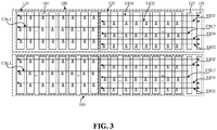
- FIG. 3 is another structural schematic diagram of a bank provided by an embodiment of the present application.
- the column decoding circuit 123 may position and select the storage arrays 104 of the first unit 110, and may further position and select the storage arrays 104 of the second unit 120.
- the first decoding selective signal line CSL1 and the second decoding selective signal line CSL2 are electrically connected to the same column decoding circuit 123.
- different banks 100 may have the independent column decoding circuit 123, or the different banks 100 may share a same column decoding circuit 123.
- the first decoding selective signal line CSL1 spans the storage arrays 104 in the first unit 110; and the second decoding selective signal line CSL2 spans the storage arrays 104 in the second unit 120.
- the first data signal line YIO1 spans the plurality of storage arrays 104, i.e., crossing the first unit 110 and the second unit 120, and is only electrically connected to the storage arrays 104 in the first unit 110; and the second data signal line YIO2 spans the storage arrays 104 in the second unit 120. More specifically, the first data signal line YIO1 is electrically connected to all storage arrays 104 in the first unit 110; and the second data signal line YIO2 is electrically connected to all storage arrays 104 in the second unit 120.
- each storage module 100 is provided with 2 sets of first data signal lines YIO1 and 2 sets of second data signal lines YIO2 is taken as an example.
- the number of sets of the first data signal lines and the second data signal lines may be designed according to an actual storage requirement.
- both the first data signal line YIO1 and the second data signal line YIO2 are electrically connected to the read-write control circuit 101.
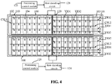
- FIG. 4 is still another structural schematic diagram of a bank provided by an embodiment of the present application.
- the storage module 100 may further include a row decoding circuit 124, configured to send a row decoding signal, to position and select either the first unit 110 or the second unit 120.
- Different banks 100 may have the independent row decoding circuit 124, or the different banks 100 may share a same row decoding circuit 124.
- the row decoding circuit 124 only enables the first decoding selective signal line CSL1 and the first column decoding circuit 102 when positioning and selecting the first unit 110; and the row decoding circuit 124 only enables the second decoding selective signal line CSL1 and the second column decoding circuit 103 when positioning and selecting the second unit 120.
- the first decoding selective signal line CSL1 and the first column decoding circuit 102 are enabled by only enabling either the first decoding selective signal line CSL1 or the second decoding selective signal line CSL2 for example, the number of the electrical contacts between the first decoding selective signal line CSL1 and the storage arrays 104 is reduced, and the number of the electrical contacts between the first data signal line YIO1 and the storage arrays 104 is also reduced.
- the short second data signal line YIO2 is beneficial to further reducing the resistance of the second data signal line YIO2 and the power consumption, thereby further reducing the power consumption of the bank.
- the bank in the write operation has the low power consumption. It is to be understood that the less load refers to that the number of storage arrays 104 electrically connected is small, i.e., the electrical contacts are few, and the parasitic capacitance is small.
- the bank may further include: a positioning control module 125, the positioning control module 125 being configured to control a row decoding signal generated by a row decoding circuit 124, such that the row decoding signal simultaneously positions and selects a first unit 110 of the high address module and a second unit 120 of the low address module, or simultaneously positions and selects a second unit 120 of the high address module and a first unit 110 of the low address module.
- the positioning control module 125 is electrically connected to the row decoding circuit 124, and is applied to sending a positioning control signal to the row decoding circuit 124; and the row decoding circuit 124 generates the row decoding signal based on the positioning control signal.
- the total lengths of the first data signal line YIO1 and the second data signal line YIO2 that are functioning for the data transmission are equal, such that the current consumption distribution of each read operation or write operation is evenly distributed, and the excessively large current peak is avoided, thereby further improving the performance of the bank.
- a situation that the bank performs the read operation is taken as an example to make descriptions in combination with the working principle of the bank.
- the first unit 110 in the high address module and the second unit 120 in the low address module are selected at the same time.
- the first data signal line YIO1 functions for data transmission
- the second data signal line YIO2 functions for data transmission
- the length of the data transmission bus is the total length of the first data signal line YIO1 and the second data signal line YIO2.
- the second unit 120 in the high address module and the first unit 110 in the low address module are selected at the same time.
- the second data signal line YIO2 functions for data transmission
- the first data signal line YIO1 functions for data transmission
- the length of the data transmission bus is the total length of the first data signal line YIO1 and the second data signal line YIO2.
- the length of the data transmission bus in each read operation keeps unchanged, so the heat consumed by the data transmission bus is the same, and the number of the loads is the same, and thus it is ensured that the current consumption is even during a working process, thereby further improving the performance of the bank.
- the working mode of the bank may also be that: the first unit of the high address module and the first unit of the low address module are selected at the same time, and the second unit of the high address module and the second unit of the low address module are selected at the same time.
- the bank provided by the embodiment has the small electric quantity consumed each time, and the corresponding bank has the advantage of the low power consumption.
- Another embodiment of the present application further provides a bank.
- the bank is approximately the same as the bank provided by the above embodiment.
- the difference lies in that the bank may further include a shift switch module, the shift switch module being configured to shift either the first data signal line or the second data signal line to be electrically connected to the read-write control circuit.
- the bank provided by the embodiment will be described below in combination with the accompanying drawings. It should be noted that parts same with or corresponding to the above embodiment may refer to the detailed descriptions on the above embodiment, and will not be repeatedly described in detail.
- FIG. 5 is a structural schematic diagram of a bank provided by another embodiment of the present application.
- FIG. 6 is a local structural schematic diagram of a bank provided by another embodiment of the present application.
- the bank may include: a storage module 100, each storage module 100 including: a read-write control circuit 101, a first column decoding circuit 102, a second column decoding circuit 103, and a plurality of storage arrays 104 arranged along a first direction; a first decoding selective signal line CSL1; a second decoding selective signal line CSL2; a first data signal line YIO1; a second data signal line YIO2; and a shift switch module 126, the shift switch module 126 being configured to shift either the first data signal line YIO1 or the second data signal line YIO2 to be electrically connected to the read-write control circuit 101.
- the column decoding circuit includes the first column decoding circuit 102 and the second column decoding circuit 103 is taken as an example. In other embodiments, there may also be only one column decoding circuit.
- the first decoding selective signal line and the second decoding selective signal line are electrically connected to the column decoding circuit.
- the shift switch module 126 includes a switch unit 136 and a control unit 146; the control unit 146 is configured to generate a control signal based on a received row decoding signal; and the switch unit 136 is configured to connect the read-write control circuit 101 and the first data signal line YIO1, or, connect the read-write control circuit 101 and the second data signal line YIO2, based on the control signal.
- the switch unit 136 includes a first switch S1 and a second switch S2, the first switch S1 is connected between the first data signal line YIO1 and the read-write control circuit 101, and the second switch S2 is connected between the second data signal line YIO2 and the read-write control circuit 101.
- the control unit 146 controls the first switch S1 to close or open, and controls the second switch S2 to close or open, based on the row decoding signal.
- the first switch S1 or the second switch S2 may be composed of at least one Metal Oxide Semiconductor (MOS) tube.
- the first switch S1 is closed, and the first data signal line YIO1 is electrically connected to the read-write control circuit 101; the first switch S1 is open, the first data signal line YIO1 is disconnected from the read-write control circuit 101; the second switch S2 is closed, and the second data signal line YIO2 is electrically connected to the read-write control circuit 101; and the second switch S2 is open, and the second data signal line YI02 is disconnected from the read-write control circuit 101.
- MOS Metal Oxide Semiconductor
- the number of switch units 136, the number of sets of the first data signal lines YIO1, and the number of sets of the second data signal lines YIO2 are the same. In the embodiment, there are two switch units 136. In other embodiments, the number of the switch units may also be reasonably provided according to the number of the sets of the first data signal lines and the second data signal lines.
- the upper storage module 100 in FIG. 5 serves as the high storage module
- the lower storage module 100 serves as the low storage module.
- the bank may further include: a positioning control module 125.
- the detailed descriptions on the positioning control module 125 may refer to the above embodiment.
- the positioning control module 125 is connected to the shift switch module 126.
- the shift switch module 126 shifts the switch based on a positioning control signal sent by the positioning control module 125, such that the first data signal line YIO1 or the second data signal line YIO2 is electrically connected to the read-write control circuit 101.
- the first switch S1 in the high address module is closed and the switch S2 is open, and the first switch S1 in the low address module is open and the second switch S2 is closed; and when the row decoding signal positions and selects a second unit 120 of the high address module and a first unit 110 of the low address module, the first switch S2 in the high address module is open and the switch S2 is closed, and the first switch S1 in the low address module is closed and the second switch S2 is open.
- the first unit 110 of the high address module and the second unit 120 of the low address module are selected; for the high address module, the first column decoding circuit 102 and the first decoding selective signal line CSL1 are enabled, the first switch S1 is closed and the second switch S2 is open, the first data signal line YIO1 is connected to the circuit, and the second data signal line YIO2 is disconnected from the circuit; and for the low address module, the second column decoding circuit 102 and the second decoding selective signal line CSL2 are enabled, the first switch S1 is open and the second switch S2 is closed, the first data signal line YIO1 is disconnected from the circuit, and the second data signal line YIO2 is connected to the circuit.
- the second unit 120 of the high address module and the first unit 110 of the low address module are selected; for the high address module, the second column decoding circuit 102 and the second decoding selective signal line CSL2 are enabled, the first switch S1 is open and the second switch S2 is closed, the first data signal line YIO1 is disconnected from the circuit, and the second data signal line YIO2 is connected to the circuit; and for the low address module, the first column decoding circuit 102 and the first decoding selective signal line CSL1 are enabled, the first switch S1 is closed and the second switch S2 is open, the first data signal line YIO1 is connected to the circuit, and the second data signal line YIO2 is disconnected from the circuit.
- the first data signal line YIO1 or the second data signal line YIO2 is completely disconnected from the circuit when not functioning for electrical signal transmission, which is beneficial to further reducing the power consumption of the bank. It is discovered through researches that when the number of storage arrays in the plurality of storage arrays is 145, the bank can save the current by 12 mA at a Baud rate of 3,733.
- Still another embodiment of the present application further provides a bank.
- the first unit and the second unit in the above embodiments are only either the high address unit or the low address unit.
- the first unit includes a first high address unit and a first low address unit
- the second unit includes a second high address unit and a second low address unit.
- the bank provided by the embodiment will be described below in combination with the accompanying drawings. It should be noted that parts same with or corresponding to the above embodiment may refer to the detailed descriptions on the above embodiment, and will not be repeatedly described in detail.
- FIG. 7 is a structural schematic diagram of a bank provided by another embodiment of the present application.
- the bank includes at least one storage module 200, each storage module 200 including: a read-write control circuit 201, a column decoding circuit and a plurality of storage arrays 204 arranged along a first direction, the plurality of storage arrays 204 being divided into at least one first unit 210 and at least one second unit 220; a first decoding selective signal line csll; a second decoding selective signal line csl2; a first data signal line yio1; and a second data signal line yio2.
- the column decoding circuit includes a first column decoding circuit 202 and a second column decoding circuit 203, the first decoding selective signal line csll is electrically connected to the first column decoding circuit 202 and the storage arrays 204 of the first unit 210, and the second decoding selective signal line csl2 is electrically connected to the second column decoding circuit 203 and the storage arrays 204 of the second unit 220.
- the first unit 210 includes a first high address unit HDQ1 and a first low address unit LDQ1; and the second unit 220 includes a second high address unit HDQ2 and a second low address unit LDQ2.
- the first low address unit HDQ1 and the second high address unit HDQ2 are adjacent, i.e., the first high address unit HDQ1, the first low address unit LDQ1, the second high address unit HDQ2, and the second low address unit LDQ2 are arranged sequentially.
- first low address unit and the second high address unit are spaced apart by the second low address unit, i.e., the second low address unit and the second high address unit may be interchangeable in position; and correspondingly, the first high address unit, the first low address unit, the second low address unit, and the second high address unit are arranged sequentially.
- the first decoding selective signal line csll is electrically connected to the first column decoding circuit 202 and all storage arrays 204 in the first unit 210, such that the first decoding selective signal line csl2 positions and selects any storage arrays 204 in the first unit 210 based on the first column decoding circuit 202; and the second decoding selective signal line csl2 is electrically connected to all storage arrays 204 in the second unit 220, such that the second decoding selective signal line csl2 positions and selects any storage arrays 204 in the second unit 220 based on the second column decoding circuit 203.
- the bank further includes a row decoding circuit, configured to send a row decoding signal, to position and select either the first unit 210 or the second unit 220.
- the first data signal line yio1 is electrically connected to the read-write control circuit 201 and all storage arrays 204 in the first high address unit HDQ1; the second data signal line yio2 is electrically connected to the read-write control circuit and all storage arrays in the second low address unit LDQ2; and the bank further includes a third data signal line yio3, the third data signal line yio3 being electrically connected to the read-write control circuit 201 and all storage arrays in the second high address unit HDQ2; and a fourth data signal line yio4, the fourth data signal line yio4 being electrically connected to the read-write control circuit 201 and all storage arrays 204 in the first low address unit LDQ1.
- FIG. 7 shows 2 sets of the first data signal lines yio1 and 2 sets of the second data signal lines yio2 in each storage module 200. It is to be understood that there may be any number of the sets of the first data signal lines yio1 and the second data signal lines yio2 in other embodiments.
- the bank includes two storage modules 200, each storage module 200 being provided with the high address unit and the low address unit.
- the bank may also only include one storage module, or, may further include any other number of storage modules.
- each storage module 200 includes one first unit 210 and one second unit 220, the bank is divided into 2 first units 210 and 2 second units 220, the first unit 210 is provided with the first high address unit HDQ1 and the first low address unit LDQ1, and the second unit is provided with the second high address unit HDQ2 and the second low address unit LDQ2, that is, each first unit 210 and each second unit 220 are provided with a high level and a low level at the same time.
- the read operation or the write operation may be performed by selecting only one first unit 210 or one second unit 220, such that the length of the first decoding selective signal line csll or the second decoding selective signal line csl2 is short and the load is significantly reduced, and the length of the first data signal line yio1, the second data signal line yio2, the third data signal line yio3 or the fourth data signal line yio4 is short and the load is significantly reduced; and in the single read operation or write operation, the total electrical contacts between the signal line and the storage arrays 204 are reduced, and the corresponding parasitic resistance and parasitic capacitance of the bank to affect the read operation and the write operation are significantly reduced. In this way, more current of the first column decoding circuit 202 and the second column decoding circuit 203 may be saved to reduce the power consumption of the bank.
- the row decoding signal selects the first unit 210 of the upper storage module 200 as an example, by only enabling the first column decoding circuit 202 and the first decoding selective signal line csll, the specified storage arrays 204 of the first high address unit HDQ1 and the specified storage arrays 204 of the first low address unit LDQ1 are positioned and selected; the first data signal line yio1 transmits a data signal between the specified storage arrays 204 in the first high address unit HDQ1 and the read-write control circuit 201; and the fourth data signal line yio4 transmits a signal before the specified storage arrays 204 in the first low address unit LDQ1 and the read-write control circuit 201. Therefore, the read operation or the write operation in the first unit 210 is completed.
- the row decoding signal selects the second unit 220 of the upper storage module 200 as an example, by only enabling the second column decoding circuit 203 and the second decoding selective signal line csl2, the specified storage arrays 204 of the second high address unit HDQ2 and the specified storage arrays 204 of the second low address unit LDQ2 are positioned and selected; the second data signal line yio2 transmits a data signal between the specified storage arrays 204 in the second high address unit LDQ2 and the read-write control circuit 201; and the third data signal line yio3 transmits a signal between the specified storage arrays 204 in the second high address unit HDQ2 and the read-write control circuit 201. Therefore, the read operation or the write operation in the second unit 220 is completed.
- the first data signal line yio1 and the third data signal line yio3 are the same bus
- the second data signal line yio2 and the fourth data signal line yio4 are the same bus
- yio1 and yio3 are labeled on the same bus
- yio2 and yio4 are labeled on the same bus in FIG. 7 . Therefore, while the structural complexity is simplified, the length of the bus is reduced, and the resistance of the bus and the consumed heat are further reduced, thereby further reducing the power consumption of the bank. It is found by researches that when the number of storage arrays in the plurality of storage arrays is 145, the bank can save the current by 10mA at a Baud rate of 3,733.
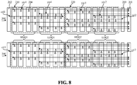
- FIG. 8 is another structural schematic diagram of the bank in the embodiment.
- the third data signal line yio3 and the first data signal line yio1 are independent of one another, i.e., being different buses; and the fourth data signal line yio4 and the second data signal line yio2 are independent of one another, i.e., being different buses.
- the number of the storage arrays 204 in the first unit 210 is the same as that of the storage arrays 204 in the second unit 220
- the number of the storage arrays 204 in the first high address unit HDQ1 is the same as that of the storage arrays 204 in the first low address unit LDQ1
- the number of the storage arrays 204 in the second high address unit HDQ2 is the same as that of the storage arrays 204 in the second low address unit LDQ2. Therefore, during each read operation or write operation, the number of the storage arrays 204 involved is the same, which is beneficial to averaging the current consumption of the bank, and avoiding the excessively large current peak, to further improve the performance of the bank.
- the number of the storage arrays in the first unit may also be different from that of the storage arrays in the second unit
- the number of the storage arrays in the first high address unit may also be different from that of the storage arrays in the first low address unit
- the number of the storage arrays in the second high address unit may also be different from that of the storage arrays in the second low address unit.
- the bank provided by the embodiment can further reduce the power consumption, and further reduce the electricity consumed.
- embodiments of the present application further provide a memory, which includes at least one bank in any one of the above embodiments.
- the column decoding circuits of different banks may be shared, may be independent of one another; and the read-write control circuits of different banks may be shared, or may be independent of one another.
- the memory may be the DRAM or Static Random Access Memory (SRAM).
- SRAM Static Random Access Memory
Landscapes
- Engineering & Computer Science (AREA)
- Microelectronics & Electronic Packaging (AREA)
- Computer Hardware Design (AREA)
- Power Engineering (AREA)
- Static Random-Access Memory (AREA)
- Dram (AREA)
- Semiconductor Memories (AREA)
Abstract
Description
- The present application claims priority to
Chinese Patent Application No. 202010237983.6, filed on March 30, 2020 - Embodiments of the present application relate to the technical field of semiconductors, and more particularly, to a memory bank and a memory.
- Dynamic Random Access Memory (DRAM) is a semiconductor storage device often used in computers, and is composed of many repetitive storage units. Each storage unit usually includes a capacitor and a transistor. A gate of the transistor is connected with a word line, a drain is connected with a bit line, and a source is connected with the capacitor. A voltage signal on the word line can control the transistor to be turned on or turned off to further read data information stored in the capacitor through the bit line or write data information in the capacitor for storage through the bit line.
- DRAM includes Double Data Rate (DDR) DRAM, Graphics Double Data Rate (GDDR) DRAM, and Low Power Double Data Rate (LPDDR) DRAM. With the application of the DRAM to more fields, for example, the increasing application of the DRAM to the mobile fields, user expectations for the speed index of the DRAM have increased.
- The performance of a DRAM at present, however, does not meet the low power consumption requirements.
- The embodiments of the disclosure provide a bank and a memory as a solution to the technical problem.
- To solve the aforementioned problems, the embodiments of the disclosure provide a bank, which includes at least one storage module, each storage module including a read-write control circuit, a column decoding circuit and a plurality of storage arrays arranged along a first direction which are divided into at least one first unit and at least one second unit. The first decoding selective signal line is electrically connected to the column decoding circuit and the storage arrays in the first unit and the second decoding selective signal line is electrically connected to the column decoding circuit and the storage arrays in the second unit. The first data signal line is electrically connected to the read-write control circuit and the storage arrays in the first unit and the second data signal line is electrically connected to the read-write control circuit and the storage arrays in the second unit.
- In addition, one first unit and one second unit are provided in which both the first unit and the second unit are a high address unit or both are a low address unit.
- In addition, the first data signal line is electrically connected to all storage arrays in the first unit and the second data signal line is electrically connected to all storage arrays in the second unit.
- In addition, the number of the storage arrays in the first unit is the same as that of the storage arrays in the second unit.
- In addition, both the first data signal line and the second data signal line are electrically connected to the read-write control circuit.
- In addition, the bank includes a shift switch module, the shift switch module being configured to electrically connect either the first data signal line or the second data signal line to the read-write control circuit.
- In addition, the shift switch module may include a control unit and a switch unit where the control unit generates a control signal based on a row decoding signal received by the control unit and, based on the control signal, the switch unit is configured to connect either the read-write control circuit with the first data signal line or the read-write control circuit with the second data signal line.
- In addition, the switch unit includes a first switch and a second switch where the first switch is connects the first data signal line and the read-write control circuit and the second switch is connects the second data signal line and the read-write control circuit.
- In addition, the bank includes two storage modules with one storage module being a high address module and the other storage module being a low address module.
- In addition, the bank includes a positioning control module where the positioning control module is configured to control a row decoding signal generated by a row decoding circuit so that the row decoding circuit simultaneously positions and selects the first unit of the high address module and the second unit of the low address module or simultaneously positions and selects the second unit of the high address module and the first unit of the low address module.
- In addition, the first unit includes a first high address unit and a first low address unit and the second unit includes a second high address unit and a second low address unit.
- In addition, the first data signal line is electrically connected to the read-write control circuit and the storage arrays in the first high address unit; the second data signal line is electrically connected to the read-write control circuit and the storage arrays in the second low address unit; and the bank may further include: a third data signal line, the third data signal line being electrically connected to the read-write control circuit and the storage arrays in the second high address unit; and a fourth data signal line, the fourth data signal line being electrically connected to the read-write control circuit and the storage arrays in the first low address unit.
- In addition, the first data signal line and the third data signal line are the same bus; and the second data signal line and the fourth data signal line are the same bus.
- In addition, the first low address unit is adjacent to the second high address unit; or the first low address unit and the second high address unit are spaced apart by the second low address unit.
- In addition, the bank includes two storage modules.
- In addition, the column decoding circuit includes: a first column decoding circuit and a second column decoding circuit, where the first decoding selective signal line is electrically connected to the first column decoding circuit and the storage arrays in the first unit, and the second decoding selective signal line is electrically connected to the second column decoding circuit and the storage arrays in the second unit.
- In addition, the first column decoding circuit and the second column decoding circuit are respectively located on the opposing sides of the plurality of storage arrays.
- The first decoding selective signal line and the second decoding selective signal line are electrically connected to the same column decoding circuit.
- In addition, the bank includes: a row decoding circuit, used to send a row decoding signal to position and select either the first unit or the second unit.
- Correspondingly, the embodiments of the application further provide memory including the bank of the aforementioned embodiment.
- Compared with existing technologies, the technical solutions provided by the application have the following advantages.
- The embodiments of the application provide the bank with an excellent structural performance, which includes a column decoding circuit that positions and selects storage arrays of the first unit and the first decoding selective signal line, a column decoding circuit that positions and selects storage arrays of the second unit and the second decoding selective signal line, a first data signal line for implementing data transmission between the storage arrays in the first unit and a read-write control circuit, and a second data signal line for implementing data transmission between the storage arrays in the second unit and the read-write control circuit. In a single read-write operation, only the first decoding selective signal line or the second decoding selective signal line is enabled. As the first decoding selective signal line is only electrically connected to part of the storage arrays, i.e., having electrical contacts, and the second decoding selective signal line is only electrically connected to part of the storage arrays, the electric contacts in the single read-write operation are reduced and the parasitic resistance and parasitic capacitance of the bank are also reduced, thus reducing a power consumption of the bank. In addition, the first data signal line and the second data signal line for the data transmission are both electrically connected to part of the storage arrays, such that the electric contacts in the single read-write operation are reduced and the parasitic resistance and parasitic capacitance of the bank are also reduced, thus reducing the power consumption of the bank.
- In addition, the bank further includes a shift switch module, where the shift switch module is configured to shift either the first data signal line or the second data signal line to electrically connect to the read-write control circuit. Therefore, when the first data signal line transmits a data signal, the second data signal line is completely disconnected from the circuit, to avoid the problem of heat loss resulting from the second data signal line, further reducing the power consumption of the bank; and likewise, when the second data signal line transmits a data signal, the first data signal line is completely disconnected from the circuit, to avoid the problem of heat loss resulting from the first data signal line, further reducing the power consumption of the bank.
- In addition, the first unit includes a first high address unit and a first low address unit, and the second unit includes a second high address unit and a second low address unit. Therefore, high data and low data can be acquired in the same unit, and only one unit is selected in each time of row decoding. This way, the bank is able to save more electricity, further reducing the power consumption of the bank.
-
-
FIG. 1 is a structural schematic diagram of a DARM. -
FIG. 2 is a structural schematic diagram of a bank provided by an embodiment of the application. -
FIG. 3 is another structural schematic diagram of a bank provided by an embodiment of the application. -
FIG. 4 is another structural schematic diagram of a bank provided by an embodiment of the application. -
FIG. 5 is a structural schematic diagram of a bank provided by another embodiment of the application. -
FIG. 6 is a local structural schematic diagram of a bank provided by another embodiment of the application. -
FIG. 7 is a structural schematic diagram of a bank provided by another embodiment of the application. -
FIG. 8 is another structural schematic diagram of a bank provided by another embodiment of the present application. - The analysis is made on the combined structural schematic diagram of the DRAM.
FIG. 1 is a structural schematic diagram of a DARM. Referring toFIG. 1 , the DRAM is composed of multiple banks 10 (also referred to as memory banks). Each bank 10 includes several storage arrays. Each storage array includes amemory array 11 and a Sense Amplifier (SA)array 12. The DRAM, regardless of whether the DDR (such as DDR2/3/4) series or the LPDDR (such as LPDDR2/3/4/5) series, divides bank 10 into a high-level group and a low-level group according to output pins (DQ). That is, each bank may also be correspondingly divided into two half banks. One half bank serves as a first module M1, and the first module M1 provides a low-level output pin; and the other half bank serves as a second module M2, and the second module M2 provides a high-level output pin. The high level and the low level refer to that whether the data bit is high or low. The low-level output pin transmits data at a low bit, and the high-level output pin transmits data at a high bit. - The decoding selective signal line CSL receives a column selective signal output by a column decoding circuit (YDEC) 13, and the data signal line YIO is configured to transmit data between the selected
memory array 11 and the read-write control circuit 14. Regardless of the half bank in the low-level group or the half bank in the high-level group, in order to smoothly complete read and write operations, the decoding selective signal line CSL has an electrical contact with eachmemory array 11 in the half bank, and the electrical contact correspondingly generates a parasitic capacitance. Both the decoding selective signal line CSL and the data signal line YIO are long, causing a large parasitic resistance, which results in the problem of large power consumption in each read and write time, resulting in high power consumption of the DRAM. - It is found through further analysis that the parasitic resistance and the parasitic capacitance are also main reasons to cause the large power consumption of the DRAM. For the decoding selective signal line CSL, in each time of the read operation or the write operation, the electrical contact between each set of decoding selective signal line CSL and each
memory array 11 has the parasitic capacitance and parasitic resistance. Like, for the data signal line YIO, in each time of the read operation or the write operation, the electrical contact between each set of data signal line YIO and eachmemory array 11 has the parasitic capacitance and parasitic resistance. Due to a number of electric contacts, the corresponding parasitic capacitances and parasitic resistances are large to cause the large power consumption of the DRAM. - In order to solve the above-mentioned problems, embodiments of the present application provide a bank with an excellent structural performance. Through the special structural design, the parasitic capacitance and parasitic resistance of the bank are reduced, thereby reducing the power consumption of the bank.
- In order to make the objectives, technical solutions and advantages of the present application clearer, embodiments of the present application are described below in detail in combination with the accompanying drawings. However, those of ordinary skill in the art may understood that many technical details are provided to better understand the present application in the embodiments of the present application. However, the technical solutions claimed by the present application may also be implemented based various changes and modifications of the following embodiments even though there are no these technical details.
-
FIG. 2 is a structural schematic diagram of a bank provided by an embodiment of the present application. - Referring to
FIG. 2 , in the embodiment, the bank may include at least one storage module 100, each storage module 100 including: a read-write control circuit 101, a column decoding circuit 123 and a plurality of storage arrays 104 arranged along a first direction, the plurality of storage arrays 104 being divided into at least one first unit 110 and at least one second unit 120; a first decoding selective signal line CSL1, the first decoding selective signal line CSL1 being electrically connected to the column decoding circuit 123 and the storage arrays 104 in the first unit 110, such that the column decoding circuit 123 positions the storage arrays 104 located in the first unit 110; a second decoding selective signal line CSL2, the second decoding selective signal line CSL2 being electrically connected to the column decoding circuit 123 and the storage arrays 104 in the second unit 120, such that the column decoding circuit 123 positions the storage arrays 104 located in the second unit 120; a first data signal line YIO1, the first data signal line YIO1 being electrically connected to the read-write control circuit 101 and the storage arrays 104 in the first unit 110; and a second data signal line YIO2, the second data signal line YIO2 being electrically connected to the read-write control circuit 101 and the storage arrays 104 in the second unit 120. - The embodiment will be described below in detail in combination with accompanying drawings. It should be noted that the triangular symbol labeled in
FIG. 2 andFIG. 3 represents a presence of the electrical connection, i.e., having the electrical contact, and the triangular symbol not labeled represents an absence of the electrical connection, i.e., not having the electrical contact, for the convenience of description. - In the embodiment, the bank includes two
storage modules 100, onestorage module 100 being a high address module, and theother storage module 100 being a low address module. For example, when the number of bits of the bank is 16 bits, the number of bits of the low address module is low 8 bits, and the number of bits of the high address module is high 8 bits. - Correspondingly, in the embodiment, one
first unit 110 and onesecond unit 120 are provided; and both thefirst unit 110 and thesecond unit 120 are a high address unit, or, both thefirst unit 110 and thesecond unit 120 are a low address unit. Thefirst unit 110 and thesecond unit 120 of onestorage module 100 are the high address units, and thestorage module 100 is referred to as the high storage module for the convenience of description. Thefirst unit 110 and thesecond unit 120 of theother storage module 100 are the low address units, and thestorage module 100 is referred to as the low storage module for the convenience of description. InFIG. 2 , a case where theupper storage module 100 serves as the high storage module, and thelower storage module 100 serves as the low storage module is taken as an example. It is understandable that the number of the first units and the second units may be designed according to an actual storage requirement in other embodiments. - Each
storage module 104 includes a memory array and a sense amplifier (SA) array. The memory array includes multiple storage elements and is configured to store data; and the SA array is configured to amplify an output signal of the memory array. Thefirst unit 110 includes the first number ofstorage arrays 104, and thesecond unit 120 may include the second number ofstorage arrays 104. The first number and the second number may be the same, or may be different. - In the embodiment, the number of the
storage arrays 104 in thefirst unit 110 is the same as that of thestorage arrays 104 in thesecond unit 120. - In the embodiment, the
column decoding circuit 123 includes: a firstcolumn decoding circuit 102 and a secondcolumn decoding circuit 103, the first decoding selective signal line CSL1 is electrically connected to the firstcolumn decoding circuit 102 and thestorage arrays 104 in thefirst unit 110, and thestorage arrays 104 in thefirst unit 110 is positioned and selected through the firstcolumn decoding circuit 102; and the second decoding selective signal line CSL2 is electrically connected to the secondcolumn decoding circuit 103 and thestorage arrays 104 in thesecond unit 120, and thestorage arrays 104 in thesecond unit 120 is positioned and selected through the secondcolumn decoding circuit 103. - The first
column decoding circuit 102 outputs a first positioning signal. Through the first decoding selective signal line CSL1, thestorage arrays 104 in thefirst unit 110 is positioned and selected, to facilitate the read operation or write operation on the selectedstorage array 104. The secondcolumn decoding circuit 103 outputs a second positioning signal. Through the second decoding selective signal line CSL2, thestorage arrays 104 in thesecond unit 120 is selected, to facilitate the read operation or write operation on the selectedstorage array 104. More specifically, the first decoding selective signal line CSL1 is electrically connected to allstorage arrays 104 in thefirst unit 110; and the second decoding selective signal line CSL2 is electrically connected to all storage arrays in thesecond unit 120. - In the embodiment, in order to further reduce the lengths of the first decoding selective signal line CSL1 and the second decoding selective signal line CSL2, and to further reduce the resistance and reduce the power consumption, the first
column decoding circuit 102 and the secondcolumn decoding circuit 103 are respectively located on two opposing sides of the plurality ofstorage arrays 104. -
FIG. 3 is another structural schematic diagram of a bank provided by an embodiment of the present application. As shown inFIG. 3 , in other embodiments, for thefirst unit 110 and thesecond unit 120, there may also be onecolumn decoding circuit 123. Thecolumn decoding circuit 123 may position and select thestorage arrays 104 of thefirst unit 110, and may further position and select thestorage arrays 104 of thesecond unit 120. The first decoding selective signal line CSL1 and the second decoding selective signal line CSL2 are electrically connected to the samecolumn decoding circuit 123. In addition,different banks 100 may have the independentcolumn decoding circuit 123, or thedifferent banks 100 may share a samecolumn decoding circuit 123. - The first decoding selective signal line CSL1 spans the
storage arrays 104 in thefirst unit 110; and the second decoding selective signal line CSL2 spans thestorage arrays 104 in thesecond unit 120. The first data signal line YIO1 spans the plurality ofstorage arrays 104, i.e., crossing thefirst unit 110 and thesecond unit 120, and is only electrically connected to thestorage arrays 104 in thefirst unit 110; and the second data signal line YIO2 spans thestorage arrays 104 in thesecond unit 120. More specifically, the first data signal line YIO1 is electrically connected to allstorage arrays 104 in thefirst unit 110; and the second data signal line YIO2 is electrically connected to allstorage arrays 104 in thesecond unit 120. - In the embodiment, a situation where each
storage module 100 is provided with 2 sets of first data signal lines YIO1 and 2 sets of second data signal lines YIO2 is taken as an example. In other embodiments, the number of sets of the first data signal lines and the second data signal lines may be designed according to an actual storage requirement. - In the embodiment, both the first data signal line YIO1 and the second data signal line YIO2 are electrically connected to the read-
write control circuit 101. - As shown in
FIG. 4, FIG. 4 is still another structural schematic diagram of a bank provided by an embodiment of the present application. Thestorage module 100 may further include arow decoding circuit 124, configured to send a row decoding signal, to position and select either thefirst unit 110 or thesecond unit 120.Different banks 100 may have the independentrow decoding circuit 124, or thedifferent banks 100 may share a samerow decoding circuit 124. - Specifically, the
row decoding circuit 124 only enables the first decoding selective signal line CSL1 and the firstcolumn decoding circuit 102 when positioning and selecting thefirst unit 110; and therow decoding circuit 124 only enables the second decoding selective signal line CSL1 and the secondcolumn decoding circuit 103 when positioning and selecting thesecond unit 120. - Compared with a solution in which all storage arrays are electrically connected with the same decoding selective signal line, in the embodiment, in the single read operation or write operation, with the case where the first decoding selective signal line CSL1 and the first
column decoding circuit 102 are enabled by only enabling either the first decoding selective signal line CSL1 or the second decoding selective signal line CSL2 for example, the number of the electrical contacts between the first decoding selective signal line CSL1 and thestorage arrays 104 is reduced, and the number of the electrical contacts between the first data signal line YIO1 and thestorage arrays 104 is also reduced. Therefore, not only can the parasitic circuit and parasitic capacitance in the bank be reduced, but the load on the first decoding selective signal line CSL1 and the first data signal line YIO1 is also significantly reduced, and thus the power consumption of the bank can be reduced remarkably. It is to be understood that when only the second decoding selective signal line CSL2 and the secondcolumn decoding circuit 103 are enabled, the power consumption of the bank can also be reduced remarkably to further reduce power consumption. - In addition, as the lengths of the second data signal line YIO2 spanning the
storage arrays 104 in thesecond unit 120 and the second data signal line YIO2 spanning thestorage arrays 104 are reduced, the short second data signal line YIO2 is beneficial to further reducing the resistance of the second data signal line YIO2 and the power consumption, thereby further reducing the power consumption of the bank. - For the convenience of understanding and description, the working principle of the write operation is described below in combination with the bank.
- In one write operation, when a row decoding signal output by the
row decoding circuit 124 points to thefirst unit 110, only the firstcolumn decoding circuit 102 and the first decoding selective signal line CSL1 are enabled, and the storage arrays in thefirst unit 110 is selected; and the first data signal line YIO1 writes data output by the read-write control circuit 101 into the selectedstorage arrays 104 in thefirst unit 110, the second decoding selective signal line CSL2 is not enabled, and the second data signal line YIO2 does not transmit a data signal. As the first decoding selective signal line CSL1 has the short length and with less load, and the load on the first data signal line YIO1 is less, the bank in the write operation has the low power consumption. It is to be understood that the less load refers to that the number ofstorage arrays 104 electrically connected is small, i.e., the electrical contacts are few, and the parasitic capacitance is small. - In another write operation, when the row decoding signal output by the
row decoding circuit 124 points to thesecond unit 120, only the secondcolumn decoding circuit 103 and the second decoding selective signal line YIO2 are enabled, and thestorage arrays 104 in thesecond unit 120 is selected; and the second data signal line YIO2 writes data output by the read-write control circuit 101 into the selectedstorage arrays 104 in thesecond unit 120, the first decoding selective signal line CSL1 is not enabled, and the first data signal line YIO1 does not transmit a data signal. As the second decoding selective signal line CSL2 has the short length and with less load, and the second data signal line YIO2 has the short length and with less load, the bank in the write operation has a low power consumption. - In the embodiment, the bank may further include: a
positioning control module 125, thepositioning control module 125 being configured to control a row decoding signal generated by arow decoding circuit 124, such that the row decoding signal simultaneously positions and selects afirst unit 110 of the high address module and asecond unit 120 of the low address module, or simultaneously positions and selects asecond unit 120 of the high address module and afirst unit 110 of the low address module. Specifically, thepositioning control module 125 is electrically connected to therow decoding circuit 124, and is applied to sending a positioning control signal to therow decoding circuit 124; and therow decoding circuit 124 generates the row decoding signal based on the positioning control signal. - Therefore, during each read operation or write operation, the total lengths of the first data signal line YIO1 and the second data signal line YIO2 that are functioning for the data transmission are equal, such that the current consumption distribution of each read operation or write operation is evenly distributed, and the excessively large current peak is avoided, thereby further improving the performance of the bank. For the convenience of understanding, a situation that the bank performs the read operation is taken as an example to make descriptions in combination with the working principle of the bank.
- In the previous read operation, the
first unit 110 in the high address module and thesecond unit 120 in the low address module are selected at the same time. For the high address module, the first data signal line YIO1 functions for data transmission; for the low address module, the second data signal line YIO2 functions for data transmission; and the length of the data transmission bus is the total length of the first data signal line YIO1 and the second data signal line YIO2. - In the later read operation, the
second unit 120 in the high address module and thefirst unit 110 in the low address module are selected at the same time. For the high address module, the second data signal line YIO2 functions for data transmission; for the low address module, the first data signal line YIO1 functions for data transmission; and the length of the data transmission bus is the total length of the first data signal line YIO1 and the second data signal line YIO2. - As can be seen from the above analysis, the length of the data transmission bus in each read operation keeps unchanged, so the heat consumed by the data transmission bus is the same, and the number of the loads is the same, and thus it is ensured that the current consumption is even during a working process, thereby further improving the performance of the bank.
- It can be understood that, in other embodiments, the working mode of the bank may also be that: the first unit of the high address module and the first unit of the low address module are selected at the same time, and the second unit of the high address module and the second unit of the low address module are selected at the same time.
- To summarize the above, the bank provided by the embodiment has the small electric quantity consumed each time, and the corresponding bank has the advantage of the low power consumption.
- Another embodiment of the present application further provides a bank. The bank is approximately the same as the bank provided by the above embodiment. The difference lies in that the bank may further include a shift switch module, the shift switch module being configured to shift either the first data signal line or the second data signal line to be electrically connected to the read-write control circuit. The bank provided by the embodiment will be described below in combination with the accompanying drawings. It should be noted that parts same with or corresponding to the above embodiment may refer to the detailed descriptions on the above embodiment, and will not be repeatedly described in detail.
-
FIG. 5 is a structural schematic diagram of a bank provided by another embodiment of the present application.FIG. 6 is a local structural schematic diagram of a bank provided by another embodiment of the present application. - Referring to
FIG. 5 andFIG. 6 , in the embodiment, the bank may include: astorage module 100, eachstorage module 100 including: a read-write control circuit 101, a firstcolumn decoding circuit 102, a secondcolumn decoding circuit 103, and a plurality ofstorage arrays 104 arranged along a first direction; a first decoding selective signal line CSL1; a second decoding selective signal line CSL2; a first data signal line YIO1; a second data signal line YIO2; and ashift switch module 126, theshift switch module 126 being configured to shift either the first data signal line YIO1 or the second data signal line YIO2 to be electrically connected to the read-write control circuit 101. - It is understandable that in the embodiment, a situation that the column decoding circuit includes the first
column decoding circuit 102 and the secondcolumn decoding circuit 103 is taken as an example. In other embodiments, there may also be only one column decoding circuit. The first decoding selective signal line and the second decoding selective signal line are electrically connected to the column decoding circuit. - As a resulting of the arrangement of the
shift switch module 126, only one the first data signal line YIO1 or the second data signal line YIO2 is connected to the circuit in the single read operation or write operation, thereby further reducing the heat consumed by the data signal line, and further reducing the power consumption of the bank. - Specifically, the
shift switch module 126 includes aswitch unit 136 and acontrol unit 146; thecontrol unit 146 is configured to generate a control signal based on a received row decoding signal; and theswitch unit 136 is configured to connect the read-write control circuit 101 and the first data signal line YIO1, or, connect the read-write control circuit 101 and the second data signal line YIO2, based on the control signal. - The
switch unit 136 includes a first switch S1 and a second switch S2, the first switch S1 is connected between the first data signal line YIO1 and the read-write control circuit 101, and the second switch S2 is connected between the second data signal line YIO2 and the read-write control circuit 101. Thecontrol unit 146 controls the first switch S1 to close or open, and controls the second switch S2 to close or open, based on the row decoding signal. - It is understandable that the first switch S1 or the second switch S2 may be composed of at least one Metal Oxide Semiconductor (MOS) tube. The first switch S1 is closed, and the first data signal line YIO1 is electrically connected to the read-
write control circuit 101; the first switch S1 is open, the first data signal line YIO1 is disconnected from the read-write control circuit 101; the second switch S2 is closed, and the second data signal line YIO2 is electrically connected to the read-write control circuit 101; and the second switch S2 is open, and the second data signal line YI02 is disconnected from the read-write control circuit 101. - For the
same storage module 100, the number ofswitch units 136, the number of sets of the first data signal lines YIO1, and the number of sets of the second data signal lines YIO2 are the same. In the embodiment, there are twoswitch units 136. In other embodiments, the number of the switch units may also be reasonably provided according to the number of the sets of the first data signal lines and the second data signal lines. - As described in the above embodiment, the
upper storage module 100 inFIG. 5 serves as the high storage module, and thelower storage module 100 serves as the low storage module. The bank may further include: apositioning control module 125. The detailed descriptions on thepositioning control module 125 may refer to the above embodiment. Thepositioning control module 125 is connected to theshift switch module 126. Theshift switch module 126 shifts the switch based on a positioning control signal sent by thepositioning control module 125, such that the first data signal line YIO1 or the second data signal line YIO2 is electrically connected to the read-write control circuit 101. - Specifically, when the row decoding signal positions and selects a
first unit 110 of the high address module and asecond unit 120 of the low address module, the first switch S1 in the high address module is closed and the switch S2 is open, and the first switch S1 in the low address module is open and the second switch S2 is closed; and when the row decoding signal positions and selects asecond unit 120 of the high address module and afirst unit 110 of the low address module, the first switch S2 in the high address module is open and the switch S2 is closed, and the first switch S1 in the low address module is closed and the second switch S2 is open. - For the convenience of understanding, the working principle of the bank provided by the embodiment will be described below in combination with the accompanying drawings.
- As shown in
FIG. 5 , in the previous write operation, thefirst unit 110 of the high address module and thesecond unit 120 of the low address module are selected; for the high address module, the firstcolumn decoding circuit 102 and the first decoding selective signal line CSL1 are enabled, the first switch S1 is closed and the second switch S2 is open, the first data signal line YIO1 is connected to the circuit, and the second data signal line YIO2 is disconnected from the circuit; and for the low address module, the secondcolumn decoding circuit 102 and the second decoding selective signal line CSL2 are enabled, the first switch S1 is open and the second switch S2 is closed, the first data signal line YIO1 is disconnected from the circuit, and the second data signal line YIO2 is connected to the circuit. - In the next write operation, the
second unit 120 of the high address module and thefirst unit 110 of the low address module are selected; for the high address module, the secondcolumn decoding circuit 102 and the second decoding selective signal line CSL2 are enabled, the first switch S1 is open and the second switch S2 is closed, the first data signal line YIO1 is disconnected from the circuit, and the second data signal line YIO2 is connected to the circuit; and for the low address module, the firstcolumn decoding circuit 102 and the first decoding selective signal line CSL1 are enabled, the first switch S1 is closed and the second switch S2 is open, the first data signal line YIO1 is connected to the circuit, and the second data signal line YIO2 is disconnected from the circuit. - Compared with the above embodiment, in this embodiment, the first data signal line YIO1 or the second data signal line YIO2 is completely disconnected from the circuit when not functioning for electrical signal transmission, which is beneficial to further reducing the power consumption of the bank. It is discovered through researches that when the number of storage arrays in the plurality of storage arrays is 145, the bank can save the current by 12 mA at a Baud rate of 3,733.
- Still another embodiment of the present application further provides a bank. Different from the above two embodiments, the first unit and the second unit in the above embodiments are only either the high address unit or the low address unit. In the embodiment, the first unit includes a first high address unit and a first low address unit, and the second unit includes a second high address unit and a second low address unit. The bank provided by the embodiment will be described below in combination with the accompanying drawings. It should be noted that parts same with or corresponding to the above embodiment may refer to the detailed descriptions on the above embodiment, and will not be repeatedly described in detail.
-
FIG. 7 is a structural schematic diagram of a bank provided by another embodiment of the present application. - Referring to
FIG. 7 , in the embodiment, the bank includes at least onestorage module 200, eachstorage module 200 including: a read-write control circuit 201, a column decoding circuit and a plurality ofstorage arrays 204 arranged along a first direction, the plurality ofstorage arrays 204 being divided into at least onefirst unit 210 and at least onesecond unit 220; a first decoding selective signal line csll; a second decoding selective signal line csl2; a first data signal line yio1; and a second data signal line yio2. - In the embodiment, the column decoding circuit includes a first
column decoding circuit 202 and a secondcolumn decoding circuit 203, the first decoding selective signal line csll is electrically connected to the firstcolumn decoding circuit 202 and thestorage arrays 204 of thefirst unit 210, and the second decoding selective signal line csl2 is electrically connected to the secondcolumn decoding circuit 203 and thestorage arrays 204 of thesecond unit 220. In other embodiments, there may also be one column decoding circuit. - The
first unit 210 includes a first high address unit HDQ1 and a first low address unit LDQ1; and thesecond unit 220 includes a second high address unit HDQ2 and a second low address unit LDQ2. In the embodiment, the first low address unit HDQ1 and the second high address unit HDQ2 are adjacent, i.e., the first high address unit HDQ1, the first low address unit LDQ1, the second high address unit HDQ2, and the second low address unit LDQ2 are arranged sequentially. - It is to be understood that in other embodiments, the first low address unit and the second high address unit are spaced apart by the second low address unit, i.e., the second low address unit and the second high address unit may be interchangeable in position; and correspondingly, the first high address unit, the first low address unit, the second low address unit, and the second high address unit are arranged sequentially.
- In the embodiment, the first decoding selective signal line csll is electrically connected to the first
column decoding circuit 202 and allstorage arrays 204 in thefirst unit 210, such that the first decoding selective signal line csl2 positions and selects anystorage arrays 204 in thefirst unit 210 based on the firstcolumn decoding circuit 202; and the second decoding selective signal line csl2 is electrically connected to allstorage arrays 204 in thesecond unit 220, such that the second decoding selective signal line csl2 positions and selects anystorage arrays 204 in thesecond unit 220 based on the secondcolumn decoding circuit 203. - In the embodiment, the bank further includes a row decoding circuit, configured to send a row decoding signal, to position and select either the
first unit 210 or thesecond unit 220. - The first data signal line yio1 is electrically connected to the read-
write control circuit 201 and allstorage arrays 204 in the first high address unit HDQ1; the second data signal line yio2 is electrically connected to the read-write control circuit and all storage arrays in the second low address unit LDQ2; and the bank further includes a third data signal line yio3, the third data signal line yio3 being electrically connected to the read-write control circuit 201 and all storage arrays in the second high address unit HDQ2; and a fourth data signal line yio4, the fourth data signal line yio4 being electrically connected to the read-write control circuit 201 and allstorage arrays 204 in the first low address unit LDQ1. -
FIG. 7 shows 2 sets of the first data signal lines yio1 and 2 sets of the second data signal lines yio2 in eachstorage module 200. It is to be understood that there may be any number of the sets of the first data signal lines yio1 and the second data signal lines yio2 in other embodiments. - In the embodiment, the bank includes two
storage modules 200, eachstorage module 200 being provided with the high address unit and the low address unit. In other embodiments, the bank may also only include one storage module, or, may further include any other number of storage modules. - Taking a case that the bank has two
storage modules 200 as an example, eachstorage module 200 includes onefirst unit 210 and onesecond unit 220, the bank is divided into 2first units second units 220, thefirst unit 210 is provided with the first high address unit HDQ1 and the first low address unit LDQ1, and the second unit is provided with the second high address unit HDQ2 and the second low address unit LDQ2, that is, eachfirst unit 210 and eachsecond unit 220 are provided with a high level and a low level at the same time. Therefore, during row decoding, the read operation or the write operation may be performed by selecting only onefirst unit 210 or onesecond unit 220, such that the length of the first decoding selective signal line csll or the second decoding selective signal line csl2 is short and the load is significantly reduced, and the length of the first data signal line yio1, the second data signal line yio2, the third data signal line yio3 or the fourth data signal line yio4 is short and the load is significantly reduced; and in the single read operation or write operation, the total electrical contacts between the signal line and thestorage arrays 204 are reduced, and the corresponding parasitic resistance and parasitic capacitance of the bank to affect the read operation and the write operation are significantly reduced. In this way, more current of the firstcolumn decoding circuit 202 and the secondcolumn decoding circuit 203 may be saved to reduce the power consumption of the bank. - For the convenience of understanding, a bank will be described below in combination with a working principle of the bank.
- Taking a case that the row decoding signal selects the
first unit 210 of theupper storage module 200 as an example, by only enabling the firstcolumn decoding circuit 202 and the first decoding selective signal line csll, the specifiedstorage arrays 204 of the first high address unit HDQ1 and the specifiedstorage arrays 204 of the first low address unit LDQ1 are positioned and selected; the first data signal line yio1 transmits a data signal between the specifiedstorage arrays 204 in the first high address unit HDQ1 and the read-write control circuit 201; and the fourth data signal line yio4 transmits a signal before the specifiedstorage arrays 204 in the first low address unit LDQ1 and the read-write control circuit 201. Therefore, the read operation or the write operation in thefirst unit 210 is completed. - Taking a case that the row decoding signal selects the
second unit 220 of theupper storage module 200 as an example, by only enabling the secondcolumn decoding circuit 203 and the second decoding selective signal line csl2, the specifiedstorage arrays 204 of the second high address unit HDQ2 and the specifiedstorage arrays 204 of the second low address unit LDQ2 are positioned and selected; the second data signal line yio2 transmits a data signal between the specifiedstorage arrays 204 in the second high address unit LDQ2 and the read-write control circuit 201; and the third data signal line yio3 transmits a signal between the specifiedstorage arrays 204 in the second high address unit HDQ2 and the read-write control circuit 201. Therefore, the read operation or the write operation in thesecond unit 220 is completed. - In the embodiment, the first data signal line yio1 and the third data signal line yio3 are the same bus, and the second data signal line yio2 and the fourth data signal line yio4 are the same bus; and for convenience of illustration and description, yio1 and yio3 are labeled on the same bus, and yio2 and yio4 are labeled on the same bus in
FIG. 7 . Therefore, while the structural complexity is simplified, the length of the bus is reduced, and the resistance of the bus and the consumed heat are further reduced, thereby further reducing the power consumption of the bank. It is found by researches that when the number of storage arrays in the plurality of storage arrays is 145, the bank can save the current by 10mA at a Baud rate of 3,733. - It should be noted that, in other embodiments, as shown in
FIG. 8, FIG. 8 is another structural schematic diagram of the bank in the embodiment. The third data signal line yio3 and the first data signal line yio1 are independent of one another, i.e., being different buses; and the fourth data signal line yio4 and the second data signal line yio2 are independent of one another, i.e., being different buses. - In the embodiment, the number of the
storage arrays 204 in thefirst unit 210 is the same as that of thestorage arrays 204 in thesecond unit 220, the number of thestorage arrays 204 in the first high address unit HDQ1 is the same as that of thestorage arrays 204 in the first low address unit LDQ1, and the number of thestorage arrays 204 in the second high address unit HDQ2 is the same as that of thestorage arrays 204 in the second low address unit LDQ2. Therefore, during each read operation or write operation, the number of thestorage arrays 204 involved is the same, which is beneficial to averaging the current consumption of the bank, and avoiding the excessively large current peak, to further improve the performance of the bank. - It is understandable that, in other embodiments, the number of the storage arrays in the first unit may also be different from that of the storage arrays in the second unit, the number of the storage arrays in the first high address unit may also be different from that of the storage arrays in the first low address unit, and the number of the storage arrays in the second high address unit may also be different from that of the storage arrays in the second low address unit.
- To summarize the above, the bank provided by the embodiment can further reduce the power consumption, and further reduce the electricity consumed.
- Correspondingly, embodiments of the present application further provide a memory, which includes at least one bank in any one of the above embodiments. The column decoding circuits of different banks may be shared, may be independent of one another; and the read-write control circuits of different banks may be shared, or may be independent of one another.
- The memory may be the DRAM or Static Random Access Memory (SRAM). As can be seen from the above analysis, the memory provided by the embodiment has the advantage of the low power consumption, and the consumed electricity is significantly reduced.
- Those of ordinary skill in the art may understand that the above embodiments are specific embodiments to implement the present application. In practical applications, various changes may be made in forms and details without departing from the spirit and scope of the present application. Any person skilled in the art may make changes and modifications without departing from the spirit and scope of the present application. Therefore, the scope of protection of the present application should be subject to the scope defined by the appended claims.
Claims (20)
- A bank, comprising at least one storage module, each one storage module comprising:a read-write control circuit, a column decoding circuit, and a plurality of storage arrays arranged along a first direction, the plurality of storage arrays being divided into at least one first unit and at least one second unit;a first decoding selective signal line, the first decoding selective signal line being electrically connected to the column decoding circuit and storage arrays in the first unit;a second decoding selective signal line, the second decoding selective signal line being electrically connected to the column decoding circuit and storage arrays in the second unit;a first data signal line, the first data signal line being electrically connected to the read-write control circuit and the storage arrays in the first unit; anda second data signal line, the second data signal line being electrically connected to the read-write control circuit and the storage arrays in the second unit.
- The bank of claim 1, whereinone first unit and one second unit are provided; andboth the first unit and the second unit are a high address unit, or, both the first unit and the second unit are a low address unit.
- The bank of claim 2, whereinthe first data signal line is electrically connected to all of the storage arrays in the first unit; andthe second data signal line is electrically connected to all of the storage arrays in the second unit.
- The bank of claim 2, wherein both the first data signal line and the second data signal line are electrically connected to the read-write control circuit.
- The bank of claim 2, further comprising: a shift switch module configured to shift either the first data signal line or the second data signal line to be electrically connected to the read-write control circuit.
- The bank of claim 5, whereinthe shift switch module comprises: a control unit and a switch unit;the control unit is configured to generate a control signal based on a row decoding signal received by the control unit; andthe switch unit is configured to connect the read-write control circuit and the first data signal line, or, connect the read-write control circuit and the second data signal line, based on the control signal.
- The bank of claim 6, whereinthe switch unit comprises a first switch and a second switch;the first switch is connected between the first data signal line and the read-write control circuit; andthe second switch is connected between the second data signal line and the read-write control circuit.
- The bank of claim 2, wherein the bank comprises two storage modules, one of the two storage modules being a high address module, and another one of the storage modules being a low address module.
- The bank of claim 8, wherein the bank further comprises: a positioning control module configured to control a row decoding signal generated by a row decoding circuit, such that the row decoding circuit simultaneously positions and selects a first unit of the high address module and a second unit of the low address module, or simultaneously positions and selects a second unit of the high address module and a first unit of the low address module.
- The bank of claim 1, whereinthe first unit comprises a first high address unit and a first low address unit; andthe second unit comprises a second high address unit and a second low address unit.
- The bank of claim 10, whereinthe first data signal line is electrically connected to the read-write control circuit and the storage arrays in the first high address unit; andthe second data signal line is electrically connected to the read-write control circuit and the storage arrays in the second low address unit.
- The bank of claim 11, further comprising:a third data signal line electrically connected to the read-write control circuit and the storage arrays in the second high address unit; anda fourth data signal line electrically connected to the read-write control circuit and the storage arrays in the first low address unit.
- The bank of claim 12, whereinthe first data signal line and the third data signal line are a same bus; andthe second data signal line and the fourth data signal line are a same bus.
- The bank of claim 13, whereinthe first low address unit is neighboring with the second high address unit; orthe first low address unit and the second high address unit are spaced apart by the second low address unit.
- The bank of claim 10, wherein the bank comprises two storage modules.
- The bank of claim 1, whereinthe column decoding circuit comprises: a first column decoding circuit and a second column decoding circuit;the first decoding selective signal line is electrically connected to the first column decoding circuit and the storage arrays in the first unit; andthe second decoding selective signal line is electrically connected to the second column decoding circuit and the storage arrays in the second unit.
- The bank of claim 16, wherein the first column decoding circuit and the second column decoding circuit are respectively located on two opposing sides of the plurality of storage arrays.
- The bank of claim 1, wherein the first decoding selective signal line and the second decoding selective signal line are electrically connected to a same column decoding circuit.
- The bank of claim 1, further comprising: a row decoding circuit, configured to send a row decoding signal, to position and select either the first unit or the second unit.
- A memory, comprising the bank of any one of claims 1 to 19.
Applications Claiming Priority (2)
| Application Number | Priority Date | Filing Date | Title |
|---|---|---|---|
| CN202010237983.6A CN113470711B (en) | 2020-03-30 | 2020-03-30 | Memory block and memory |
| PCT/CN2021/073981 WO2021196853A1 (en) | 2020-03-30 | 2021-01-27 | Memory block and memory |
Publications (3)
| Publication Number | Publication Date |
|---|---|
| EP3933839A1 true EP3933839A1 (en) | 2022-01-05 |
| EP3933839A4 EP3933839A4 (en) | 2022-08-24 |
| EP3933839B1 EP3933839B1 (en) | 2024-01-10 |
Family
ID=77865016
Family Applications (1)
| Application Number | Title | Priority Date | Filing Date |
|---|---|---|---|
| EP21773437.5A Active EP3933839B1 (en) | 2020-03-30 | 2021-01-27 | Memory block and memory |
Country Status (4)
| Country | Link |
|---|---|
| US (1) | US11869578B2 (en) |
| EP (1) | EP3933839B1 (en) |
| CN (1) | CN113470711B (en) |
| WO (1) | WO2021196853A1 (en) |
Families Citing this family (17)
| Publication number | Priority date | Publication date | Assignee | Title |
|---|---|---|---|---|
| CN115440268B (en) | 2021-06-01 | 2024-07-12 | 长鑫存储技术有限公司 | Memory |
| CN115424654B (en) | 2021-06-01 | 2024-07-05 | 长鑫存储技术有限公司 | Memory |
| CN116264088B (en) * | 2021-12-15 | 2025-06-20 | 长鑫存储技术有限公司 | Memory |
| CN116264089B (en) * | 2021-12-15 | 2025-06-06 | 长鑫存储技术有限公司 | Memory |
| CN116343853B (en) * | 2021-12-23 | 2025-06-27 | 长鑫存储技术有限公司 | Memory block and memory |
| US12176054B2 (en) | 2021-12-23 | 2024-12-24 | Changxin Memory Technologies, Inc. | Memory bank and memory |
| US12374389B2 (en) | 2021-12-23 | 2025-07-29 | Changxin Memory Technologies, Inc. | Memory bank and memory |
| KR102838329B1 (en) | 2022-02-24 | 2025-07-23 | 창신 메모리 테크놀로지즈 아이엔씨 | Data transmission circuit, data transmission method and memory |
| JP7660717B2 (en) | 2022-02-24 | 2025-04-11 | チャンシン メモリー テクノロジーズ インコーポレイテッド | Data error correction circuit and data transmission circuit |
| US11928341B2 (en) | 2022-02-24 | 2024-03-12 | Changxin Memory Technologies, Inc. | Sleep control method and sleep control circuit |
| EP4258116A4 (en) | 2022-02-24 | 2024-01-03 | Changxin Memory Technologies, Inc. | DATA TRANSMISSION CIRCUIT AND DATA TRANSMISSION METHOD |
| CN116705105B (en) * | 2022-02-24 | 2024-12-06 | 长鑫存储技术有限公司 | Storage circuits, data transmission circuits and memories |
| US12009024B2 (en) | 2022-03-03 | 2024-06-11 | Changxin Memory Technologies, Inc. | Circuit for reading out data, method for reading out data and memory |
| CN116741224B (en) * | 2022-03-03 | 2024-12-06 | 长鑫存储技术有限公司 | Data writing circuit, data writing method memory |
| US12131059B2 (en) | 2022-03-03 | 2024-10-29 | Changxin Memory Technologies, Inc. | Data writing circuit, data writing method, and memory |
| CN118366511A (en) * | 2023-01-12 | 2024-07-19 | 长鑫存储技术有限公司 | Storage circuit and memory thereof |
| CN119068921B (en) * | 2023-05-26 | 2025-10-03 | 长鑫存储技术有限公司 | Memory and electronic device |
Family Cites Families (22)
| Publication number | Priority date | Publication date | Assignee | Title |
|---|---|---|---|---|
| JP3476231B2 (en) | 1993-01-29 | 2003-12-10 | 三菱電機エンジニアリング株式会社 | Synchronous semiconductor memory device and semiconductor memory device |
| KR960006271B1 (en) * | 1993-08-14 | 1996-05-13 | 삼성전자주식회사 | Semiconductor memory device with I / O line driving method for high speed operation |
| JP4118364B2 (en) * | 1997-07-16 | 2008-07-16 | 日本テキサス・インスツルメンツ株式会社 | Semiconductor memory device |
| JPH11162174A (en) * | 1997-11-25 | 1999-06-18 | Mitsubishi Electric Corp | Synchronous semiconductor memory device |
| JP4819258B2 (en) * | 2001-08-13 | 2011-11-24 | ルネサスエレクトロニクス株式会社 | Semiconductor memory device |
| US6798712B2 (en) | 2002-07-02 | 2004-09-28 | Advanced Micro Devices, Inc. | Wordline latching in semiconductor memories |
| JP4152736B2 (en) * | 2002-12-11 | 2008-09-17 | 株式会社ルネサステクノロジ | Semiconductor memory device |
| KR100538883B1 (en) | 2003-04-29 | 2005-12-23 | 주식회사 하이닉스반도체 | Semiconductor memory apparatus |
| JP2006216136A (en) * | 2005-02-02 | 2006-08-17 | Toshiba Corp | Semiconductor memory device |
| KR100678643B1 (en) * | 2005-12-15 | 2007-02-05 | 삼성전자주식회사 | Multilevel Dynamic Memory Device |
| US7359252B2 (en) | 2006-01-09 | 2008-04-15 | Infineon Technologies Ag | Memory data bus structure and method of transferring information with plural memory banks |
| US8120985B2 (en) | 2008-03-12 | 2012-02-21 | Qimonda Ag | Multi-bank memory device method and apparatus |
| CN102024491B (en) | 2009-09-22 | 2013-07-24 | 无锡华润上华半导体有限公司 | Random access memory and control method thereof |
| CN102376346B (en) | 2010-08-20 | 2014-02-12 | 华邦电子股份有限公司 | Dynamic random access memory unit and its data update method |
| TWI539453B (en) * | 2010-09-14 | 2016-06-21 | 半導體能源研究所股份有限公司 | Memory device and semiconductor device |
| CN102932610B (en) * | 2012-10-15 | 2016-03-23 | 清华大学 | A kind of image sensor array structure based on flash memory |
| CN103943138B (en) | 2014-04-18 | 2017-01-11 | 中国科学院上海高等研究院 | Per unit multi-bit storage device |
| TWI552162B (en) | 2014-07-31 | 2016-10-01 | Zhi-Cheng Xiao | Low power memory |
| CN105261391B (en) * | 2015-09-30 | 2018-08-10 | 展讯通信(上海)有限公司 | A kind of SRAM storage arrays |
| CN106251892B (en) * | 2016-08-23 | 2024-08-16 | 格科微电子(上海)有限公司 | High capacity memory |
| CN110111833B (en) * | 2019-04-03 | 2021-07-13 | 中国科学院微电子研究所 | Memory verification circuit and verification method |
| JP2021150002A (en) * | 2020-03-23 | 2021-09-27 | 株式会社東芝 | Semiconductor storage device and semiconductor storage device control method |
-
2020
- 2020-03-30 CN CN202010237983.6A patent/CN113470711B/en active Active
-
2021
- 2021-01-27 EP EP21773437.5A patent/EP3933839B1/en active Active
- 2021-01-27 WO PCT/CN2021/073981 patent/WO2021196853A1/en not_active Ceased
- 2021-09-13 US US17/447,569 patent/US11869578B2/en active Active
Also Published As
| Publication number | Publication date |
|---|---|
| US11869578B2 (en) | 2024-01-09 |
| CN113470711B (en) | 2023-06-16 |
| EP3933839B1 (en) | 2024-01-10 |
| CN113470711A (en) | 2021-10-01 |
| EP3933839A4 (en) | 2022-08-24 |
| US20210407576A1 (en) | 2021-12-30 |
| WO2021196853A1 (en) | 2021-10-07 |
Similar Documents
| Publication | Publication Date | Title |
|---|---|---|
| EP3933839B1 (en) | Memory block and memory | |
| US11538515B2 (en) | DRAM memory | |
| US9412432B2 (en) | Semiconductor storage device and system provided with same | |
| US12468442B2 (en) | Techniques for power management using loopback | |
| US10409741B2 (en) | Semiconductor memory apparatus and data input/output method thereof | |
| JP2022528913A (en) | Memory array with multiplexed digit lines | |
| CN212303080U (en) | Sense amplifier and memory device | |
| TWI764344B (en) | Apparatus for enhancing prefetch access in memory module | |
| CN113870911A (en) | Sensitive amplifier, storage device and read-write method | |
| EP4273710A2 (en) | Memory system and operations of the same | |
| JP2023147215A (en) | Memory unit and layouts thereof | |
| US20210407558A1 (en) | Sense amplifier, storage device and read-write method | |
| US12176054B2 (en) | Memory bank and memory | |
| CN104751876A (en) | Dual port SRAM (static random access memory) structure | |
| KR100668513B1 (en) | Semiconductor memory device | |
| CN116264087A (en) | memory | |
| CN112837717A (en) | Apparatus for increasing the number of data prefetches in a memory module | |
| CN116264088A (en) | memory | |
| CN116343853B (en) | Memory block and memory | |
| CN116343891B (en) | Storage blocks and memory | |
| EP4350921B1 (en) | Power source providing circuit and memory | |
| CN114155896B (en) | Semiconductor device with a semiconductor device having a plurality of semiconductor chips | |
| US11721390B2 (en) | DRAM with inter-section, page-data-copy scheme for low power and wide data access | |
| US11848045B2 (en) | Memory integrated circuit with local amplifier module and local read-write conversion module to improve operation speed and reduce number of data lines | |
| CN121999835A (en) | Static memory and manufacturing method thereof |
Legal Events
| Date | Code | Title | Description |
|---|---|---|---|
| STAA | Information on the status of an ep patent application or granted ep patent |
Free format text: STATUS: UNKNOWN |
|
| STAA | Information on the status of an ep patent application or granted ep patent |
Free format text: STATUS: THE INTERNATIONAL PUBLICATION HAS BEEN MADE |
|
| PUAI | Public reference made under article 153(3) epc to a published international application that has entered the european phase |
Free format text: ORIGINAL CODE: 0009012 |
|
| STAA | Information on the status of an ep patent application or granted ep patent |
Free format text: STATUS: REQUEST FOR EXAMINATION WAS MADE |
|
| 17P | Request for examination filed |
Effective date: 20210930 |
|
| AK | Designated contracting states |
Kind code of ref document: A1 Designated state(s): AL AT BE BG CH CY CZ DE DK EE ES FI FR GB GR HR HU IE IS IT LI LT LU LV MC MK MT NL NO PL PT RO RS SE SI SK SM TR |
|
| A4 | Supplementary search report drawn up and despatched |
Effective date: 20220725 |
|
| RIC1 | Information provided on ipc code assigned before grant |
Ipc: G11C 11/4091 20060101ALI20220719BHEP Ipc: G11C 11/4097 20060101ALI20220719BHEP Ipc: G11C 11/408 20060101AFI20220719BHEP |
|
| STAA | Information on the status of an ep patent application or granted ep patent |
Free format text: STATUS: EXAMINATION IS IN PROGRESS |
|
| 17Q | First examination report despatched |
Effective date: 20230313 |
|
| DAV | Request for validation of the european patent (deleted) | ||
| DAX | Request for extension of the european patent (deleted) | ||
| GRAP | Despatch of communication of intention to grant a patent |
Free format text: ORIGINAL CODE: EPIDOSNIGR1 |
|
| STAA | Information on the status of an ep patent application or granted ep patent |
Free format text: STATUS: GRANT OF PATENT IS INTENDED |
|
| INTG | Intention to grant announced |
Effective date: 20230915 |
|
| P01 | Opt-out of the competence of the unified patent court (upc) registered |
Effective date: 20231018 |
|
| GRAS | Grant fee paid |
Free format text: ORIGINAL CODE: EPIDOSNIGR3 |
|
| GRAA | (expected) grant |
Free format text: ORIGINAL CODE: 0009210 |
|
| STAA | Information on the status of an ep patent application or granted ep patent |
Free format text: STATUS: THE PATENT HAS BEEN GRANTED |
|
| AK | Designated contracting states |
Kind code of ref document: B1 Designated state(s): AL AT BE BG CH CY CZ DE DK EE ES FI FR GB GR HR HU IE IS IT LI LT LU LV MC MK MT NL NO PL PT RO RS SE SI SK SM TR |
|
| REG | Reference to a national code |
Ref country code: GB Ref legal event code: FG4D |
|
| REG | Reference to a national code |
Ref country code: CH Ref legal event code: EP |
|
| REG | Reference to a national code |
Ref country code: DE Ref legal event code: R096 Ref document number: 602021008583 Country of ref document: DE |
|
| REG | Reference to a national code |
Ref country code: IE Ref legal event code: FG4D |
|
| REG | Reference to a national code |
Ref country code: LT Ref legal event code: MG9D |
|
| REG | Reference to a national code |
Ref country code: NL Ref legal event code: MP Effective date: 20240110 |
|
| REG | Reference to a national code |
Ref country code: AT Ref legal event code: MK05 Ref document number: 1649558 Country of ref document: AT Kind code of ref document: T Effective date: 20240110 |
|
| PG25 | Lapsed in a contracting state [announced via postgrant information from national office to epo] |
Ref country code: NL Free format text: LAPSE BECAUSE OF FAILURE TO SUBMIT A TRANSLATION OF THE DESCRIPTION OR TO PAY THE FEE WITHIN THE PRESCRIBED TIME-LIMIT Effective date: 20240110 |
|
| PG25 | Lapsed in a contracting state [announced via postgrant information from national office to epo] |
Ref country code: NL Free format text: LAPSE BECAUSE OF FAILURE TO SUBMIT A TRANSLATION OF THE DESCRIPTION OR TO PAY THE FEE WITHIN THE PRESCRIBED TIME-LIMIT Effective date: 20240110 |
|
| PG25 | Lapsed in a contracting state [announced via postgrant information from national office to epo] |
Ref country code: IS Free format text: LAPSE BECAUSE OF FAILURE TO SUBMIT A TRANSLATION OF THE DESCRIPTION OR TO PAY THE FEE WITHIN THE PRESCRIBED TIME-LIMIT Effective date: 20240510 |
|
| PG25 | Lapsed in a contracting state [announced via postgrant information from national office to epo] |
Ref country code: LT Free format text: LAPSE BECAUSE OF FAILURE TO SUBMIT A TRANSLATION OF THE DESCRIPTION OR TO PAY THE FEE WITHIN THE PRESCRIBED TIME-LIMIT Effective date: 20240110 |
|
| PG25 | Lapsed in a contracting state [announced via postgrant information from national office to epo] |
Ref country code: GR Free format text: LAPSE BECAUSE OF FAILURE TO SUBMIT A TRANSLATION OF THE DESCRIPTION OR TO PAY THE FEE WITHIN THE PRESCRIBED TIME-LIMIT Effective date: 20240411 |
|
| PG25 | Lapsed in a contracting state [announced via postgrant information from national office to epo] |
Ref country code: RS Free format text: LAPSE BECAUSE OF FAILURE TO SUBMIT A TRANSLATION OF THE DESCRIPTION OR TO PAY THE FEE WITHIN THE PRESCRIBED TIME-LIMIT Effective date: 20240410 Ref country code: HR Free format text: LAPSE BECAUSE OF FAILURE TO SUBMIT A TRANSLATION OF THE DESCRIPTION OR TO PAY THE FEE WITHIN THE PRESCRIBED TIME-LIMIT Effective date: 20240110 |
|
| PG25 | Lapsed in a contracting state [announced via postgrant information from national office to epo] |
Ref country code: ES Free format text: LAPSE BECAUSE OF FAILURE TO SUBMIT A TRANSLATION OF THE DESCRIPTION OR TO PAY THE FEE WITHIN THE PRESCRIBED TIME-LIMIT Effective date: 20240110 |
|
| PG25 | Lapsed in a contracting state [announced via postgrant information from national office to epo] |
Ref country code: AT Free format text: LAPSE BECAUSE OF FAILURE TO SUBMIT A TRANSLATION OF THE DESCRIPTION OR TO PAY THE FEE WITHIN THE PRESCRIBED TIME-LIMIT Effective date: 20240110 |
|
| PG25 | Lapsed in a contracting state [announced via postgrant information from national office to epo] |
Ref country code: RS Free format text: LAPSE BECAUSE OF FAILURE TO SUBMIT A TRANSLATION OF THE DESCRIPTION OR TO PAY THE FEE WITHIN THE PRESCRIBED TIME-LIMIT Effective date: 20240410 Ref country code: NO Free format text: LAPSE BECAUSE OF FAILURE TO SUBMIT A TRANSLATION OF THE DESCRIPTION OR TO PAY THE FEE WITHIN THE PRESCRIBED TIME-LIMIT Effective date: 20240410 Ref country code: LT Free format text: LAPSE BECAUSE OF FAILURE TO SUBMIT A TRANSLATION OF THE DESCRIPTION OR TO PAY THE FEE WITHIN THE PRESCRIBED TIME-LIMIT Effective date: 20240110 Ref country code: IS Free format text: LAPSE BECAUSE OF FAILURE TO SUBMIT A TRANSLATION OF THE DESCRIPTION OR TO PAY THE FEE WITHIN THE PRESCRIBED TIME-LIMIT Effective date: 20240510 Ref country code: HR Free format text: LAPSE BECAUSE OF FAILURE TO SUBMIT A TRANSLATION OF THE DESCRIPTION OR TO PAY THE FEE WITHIN THE PRESCRIBED TIME-LIMIT Effective date: 20240110 Ref country code: GR Free format text: LAPSE BECAUSE OF FAILURE TO SUBMIT A TRANSLATION OF THE DESCRIPTION OR TO PAY THE FEE WITHIN THE PRESCRIBED TIME-LIMIT Effective date: 20240411 Ref country code: ES Free format text: LAPSE BECAUSE OF FAILURE TO SUBMIT A TRANSLATION OF THE DESCRIPTION OR TO PAY THE FEE WITHIN THE PRESCRIBED TIME-LIMIT Effective date: 20240110 Ref country code: BG Free format text: LAPSE BECAUSE OF FAILURE TO SUBMIT A TRANSLATION OF THE DESCRIPTION OR TO PAY THE FEE WITHIN THE PRESCRIBED TIME-LIMIT Effective date: 20240110 Ref country code: AT Free format text: LAPSE BECAUSE OF FAILURE TO SUBMIT A TRANSLATION OF THE DESCRIPTION OR TO PAY THE FEE WITHIN THE PRESCRIBED TIME-LIMIT Effective date: 20240110 |
|
| PG25 | Lapsed in a contracting state [announced via postgrant information from national office to epo] |
Ref country code: PT Free format text: LAPSE BECAUSE OF FAILURE TO SUBMIT A TRANSLATION OF THE DESCRIPTION OR TO PAY THE FEE WITHIN THE PRESCRIBED TIME-LIMIT Effective date: 20240510 Ref country code: PL Free format text: LAPSE BECAUSE OF FAILURE TO SUBMIT A TRANSLATION OF THE DESCRIPTION OR TO PAY THE FEE WITHIN THE PRESCRIBED TIME-LIMIT Effective date: 20240110 |
|
| PG25 | Lapsed in a contracting state [announced via postgrant information from national office to epo] |
Ref country code: SE Free format text: LAPSE BECAUSE OF FAILURE TO SUBMIT A TRANSLATION OF THE DESCRIPTION OR TO PAY THE FEE WITHIN THE PRESCRIBED TIME-LIMIT Effective date: 20240110 Ref country code: PT Free format text: LAPSE BECAUSE OF FAILURE TO SUBMIT A TRANSLATION OF THE DESCRIPTION OR TO PAY THE FEE WITHIN THE PRESCRIBED TIME-LIMIT Effective date: 20240510 Ref country code: PL Free format text: LAPSE BECAUSE OF FAILURE TO SUBMIT A TRANSLATION OF THE DESCRIPTION OR TO PAY THE FEE WITHIN THE PRESCRIBED TIME-LIMIT Effective date: 20240110 Ref country code: LV Free format text: LAPSE BECAUSE OF FAILURE TO SUBMIT A TRANSLATION OF THE DESCRIPTION OR TO PAY THE FEE WITHIN THE PRESCRIBED TIME-LIMIT Effective date: 20240110 |
|
| REG | Reference to a national code |
Ref country code: CH Ref legal event code: PL |
|
| PG25 | Lapsed in a contracting state [announced via postgrant information from national office to epo] |
Ref country code: LU Free format text: LAPSE BECAUSE OF NON-PAYMENT OF DUE FEES Effective date: 20240127 |
|
| PG25 | Lapsed in a contracting state [announced via postgrant information from national office to epo] |
Ref country code: LU Free format text: LAPSE BECAUSE OF NON-PAYMENT OF DUE FEES Effective date: 20240127 |
|
| PG25 | Lapsed in a contracting state [announced via postgrant information from national office to epo] |
Ref country code: DK Free format text: LAPSE BECAUSE OF FAILURE TO SUBMIT A TRANSLATION OF THE DESCRIPTION OR TO PAY THE FEE WITHIN THE PRESCRIBED TIME-LIMIT Effective date: 20240110 |
|
| REG | Reference to a national code |
Ref country code: DE Ref legal event code: R097 Ref document number: 602021008583 Country of ref document: DE |
|
| PG25 | Lapsed in a contracting state [announced via postgrant information from national office to epo] |
Ref country code: SM Free format text: LAPSE BECAUSE OF FAILURE TO SUBMIT A TRANSLATION OF THE DESCRIPTION OR TO PAY THE FEE WITHIN THE PRESCRIBED TIME-LIMIT Effective date: 20240110 |
|
| PG25 | Lapsed in a contracting state [announced via postgrant information from national office to epo] |
Ref country code: BE Free format text: LAPSE BECAUSE OF NON-PAYMENT OF DUE FEES Effective date: 20240131 |
|
| PG25 | Lapsed in a contracting state [announced via postgrant information from national office to epo] |
Ref country code: CH Free format text: LAPSE BECAUSE OF NON-PAYMENT OF DUE FEES Effective date: 20240131 |
|
| PG25 | Lapsed in a contracting state [announced via postgrant information from national office to epo] |
Ref country code: CZ Free format text: LAPSE BECAUSE OF FAILURE TO SUBMIT A TRANSLATION OF THE DESCRIPTION OR TO PAY THE FEE WITHIN THE PRESCRIBED TIME-LIMIT Effective date: 20240110 Ref country code: EE Free format text: LAPSE BECAUSE OF FAILURE TO SUBMIT A TRANSLATION OF THE DESCRIPTION OR TO PAY THE FEE WITHIN THE PRESCRIBED TIME-LIMIT Effective date: 20240110 |
|
| PG25 | Lapsed in a contracting state [announced via postgrant information from national office to epo] |
Ref country code: SK Free format text: LAPSE BECAUSE OF FAILURE TO SUBMIT A TRANSLATION OF THE DESCRIPTION OR TO PAY THE FEE WITHIN THE PRESCRIBED TIME-LIMIT Effective date: 20240110 |
|
| PG25 | Lapsed in a contracting state [announced via postgrant information from national office to epo] |
Ref country code: SM Free format text: LAPSE BECAUSE OF FAILURE TO SUBMIT A TRANSLATION OF THE DESCRIPTION OR TO PAY THE FEE WITHIN THE PRESCRIBED TIME-LIMIT Effective date: 20240110 Ref country code: SK Free format text: LAPSE BECAUSE OF FAILURE TO SUBMIT A TRANSLATION OF THE DESCRIPTION OR TO PAY THE FEE WITHIN THE PRESCRIBED TIME-LIMIT Effective date: 20240110 Ref country code: RO Free format text: LAPSE BECAUSE OF FAILURE TO SUBMIT A TRANSLATION OF THE DESCRIPTION OR TO PAY THE FEE WITHIN THE PRESCRIBED TIME-LIMIT Effective date: 20240110 Ref country code: EE Free format text: LAPSE BECAUSE OF FAILURE TO SUBMIT A TRANSLATION OF THE DESCRIPTION OR TO PAY THE FEE WITHIN THE PRESCRIBED TIME-LIMIT Effective date: 20240110 Ref country code: DK Free format text: LAPSE BECAUSE OF FAILURE TO SUBMIT A TRANSLATION OF THE DESCRIPTION OR TO PAY THE FEE WITHIN THE PRESCRIBED TIME-LIMIT Effective date: 20240110 Ref country code: CZ Free format text: LAPSE BECAUSE OF FAILURE TO SUBMIT A TRANSLATION OF THE DESCRIPTION OR TO PAY THE FEE WITHIN THE PRESCRIBED TIME-LIMIT Effective date: 20240110 Ref country code: CH Free format text: LAPSE BECAUSE OF NON-PAYMENT OF DUE FEES Effective date: 20240131 Ref country code: BE Free format text: LAPSE BECAUSE OF NON-PAYMENT OF DUE FEES Effective date: 20240131 |
|
| REG | Reference to a national code |
Ref country code: BE Ref legal event code: MM Effective date: 20240131 |
|
| PG25 | Lapsed in a contracting state [announced via postgrant information from national office to epo] |
Ref country code: MC Free format text: LAPSE BECAUSE OF FAILURE TO SUBMIT A TRANSLATION OF THE DESCRIPTION OR TO PAY THE FEE WITHIN THE PRESCRIBED TIME-LIMIT Effective date: 20240110 |
|
| PLBE | No opposition filed within time limit |
Free format text: ORIGINAL CODE: 0009261 |
|
| STAA | Information on the status of an ep patent application or granted ep patent |
Free format text: STATUS: NO OPPOSITION FILED WITHIN TIME LIMIT |
|
| PG25 | Lapsed in a contracting state [announced via postgrant information from national office to epo] |
Ref country code: MC Free format text: LAPSE BECAUSE OF FAILURE TO SUBMIT A TRANSLATION OF THE DESCRIPTION OR TO PAY THE FEE WITHIN THE PRESCRIBED TIME-LIMIT Effective date: 20240110 |
|
| PG25 | Lapsed in a contracting state [announced via postgrant information from national office to epo] |
Ref country code: IT Free format text: LAPSE BECAUSE OF FAILURE TO SUBMIT A TRANSLATION OF THE DESCRIPTION OR TO PAY THE FEE WITHIN THE PRESCRIBED TIME-LIMIT Effective date: 20240110 |
|
| 26N | No opposition filed |
Effective date: 20241011 |
|
| PG25 | Lapsed in a contracting state [announced via postgrant information from national office to epo] |
Ref country code: IT Free format text: LAPSE BECAUSE OF FAILURE TO SUBMIT A TRANSLATION OF THE DESCRIPTION OR TO PAY THE FEE WITHIN THE PRESCRIBED TIME-LIMIT Effective date: 20240110 |
|
| PG25 | Lapsed in a contracting state [announced via postgrant information from national office to epo] |
Ref country code: IE Free format text: LAPSE BECAUSE OF NON-PAYMENT OF DUE FEES Effective date: 20240127 |
|
| PG25 | Lapsed in a contracting state [announced via postgrant information from national office to epo] |
Ref country code: IE Free format text: LAPSE BECAUSE OF NON-PAYMENT OF DUE FEES Effective date: 20240127 |
|
| PG25 | Lapsed in a contracting state [announced via postgrant information from national office to epo] |
Ref country code: SI Free format text: LAPSE BECAUSE OF FAILURE TO SUBMIT A TRANSLATION OF THE DESCRIPTION OR TO PAY THE FEE WITHIN THE PRESCRIBED TIME-LIMIT Effective date: 20240110 |
|
| PG25 | Lapsed in a contracting state [announced via postgrant information from national office to epo] |
Ref country code: CY Free format text: LAPSE BECAUSE OF FAILURE TO SUBMIT A TRANSLATION OF THE DESCRIPTION OR TO PAY THE FEE WITHIN THE PRESCRIBED TIME-LIMIT; INVALID AB INITIO Effective date: 20210127 |
|
| PG25 | Lapsed in a contracting state [announced via postgrant information from national office to epo] |
Ref country code: HU Free format text: LAPSE BECAUSE OF FAILURE TO SUBMIT A TRANSLATION OF THE DESCRIPTION OR TO PAY THE FEE WITHIN THE PRESCRIBED TIME-LIMIT; INVALID AB INITIO Effective date: 20210127 |
|
| PG25 | Lapsed in a contracting state [announced via postgrant information from national office to epo] |
Ref country code: FI Free format text: LAPSE BECAUSE OF FAILURE TO SUBMIT A TRANSLATION OF THE DESCRIPTION OR TO PAY THE FEE WITHIN THE PRESCRIBED TIME-LIMIT Effective date: 20240110 |
|
| PG25 | Lapsed in a contracting state [announced via postgrant information from national office to epo] |
Ref country code: TR Free format text: LAPSE BECAUSE OF FAILURE TO SUBMIT A TRANSLATION OF THE DESCRIPTION OR TO PAY THE FEE WITHIN THE PRESCRIBED TIME-LIMIT Effective date: 20240110 |
|
| PGFP | Annual fee paid to national office [announced via postgrant information from national office to epo] |
Ref country code: GB Payment date: 20260123 Year of fee payment: 6 |
|
| PGFP | Annual fee paid to national office [announced via postgrant information from national office to epo] |
Ref country code: DE Payment date: 20260121 Year of fee payment: 6 |
|
| PGFP | Annual fee paid to national office [announced via postgrant information from national office to epo] |
Ref country code: FR Payment date: 20260123 Year of fee payment: 6 |