EP3929335A1 - Semiconductor wafer made of single-crystal silicon and process for the production thereof - Google Patents
Semiconductor wafer made of single-crystal silicon and process for the production thereof Download PDFInfo
- Publication number
- EP3929335A1 EP3929335A1 EP20182286.3A EP20182286A EP3929335A1 EP 3929335 A1 EP3929335 A1 EP 3929335A1 EP 20182286 A EP20182286 A EP 20182286A EP 3929335 A1 EP3929335 A1 EP 3929335A1
- Authority
- EP
- European Patent Office
- Prior art keywords
- semiconductor wafer
- less
- atoms
- sup
- epitaxial layer
- Prior art date
- Legal status (The legal status is an assumption and is not a legal conclusion. Google has not performed a legal analysis and makes no representation as to the accuracy of the status listed.)
- Pending
Links
Images


Classifications
-
- C—CHEMISTRY; METALLURGY
- C30—CRYSTAL GROWTH
- C30B—SINGLE-CRYSTAL GROWTH; UNIDIRECTIONAL SOLIDIFICATION OF EUTECTIC MATERIAL OR UNIDIRECTIONAL DEMIXING OF EUTECTOID MATERIAL; REFINING BY ZONE-MELTING OF MATERIAL; PRODUCTION OF A HOMOGENEOUS POLYCRYSTALLINE MATERIAL WITH DEFINED STRUCTURE; SINGLE CRYSTALS OR HOMOGENEOUS POLYCRYSTALLINE MATERIAL WITH DEFINED STRUCTURE; AFTER-TREATMENT OF SINGLE CRYSTALS OR A HOMOGENEOUS POLYCRYSTALLINE MATERIAL WITH DEFINED STRUCTURE; APPARATUS THEREFOR
- C30B15/00—Single-crystal growth by pulling from a melt, e.g. Czochralski method
- C30B15/20—Controlling or regulating
- C30B15/203—Controlling or regulating the relationship of pull rate (v) to axial thermal gradient (G)
-
- C—CHEMISTRY; METALLURGY
- C30—CRYSTAL GROWTH
- C30B—SINGLE-CRYSTAL GROWTH; UNIDIRECTIONAL SOLIDIFICATION OF EUTECTIC MATERIAL OR UNIDIRECTIONAL DEMIXING OF EUTECTOID MATERIAL; REFINING BY ZONE-MELTING OF MATERIAL; PRODUCTION OF A HOMOGENEOUS POLYCRYSTALLINE MATERIAL WITH DEFINED STRUCTURE; SINGLE CRYSTALS OR HOMOGENEOUS POLYCRYSTALLINE MATERIAL WITH DEFINED STRUCTURE; AFTER-TREATMENT OF SINGLE CRYSTALS OR A HOMOGENEOUS POLYCRYSTALLINE MATERIAL WITH DEFINED STRUCTURE; APPARATUS THEREFOR
- C30B15/00—Single-crystal growth by pulling from a melt, e.g. Czochralski method
- C30B15/20—Controlling or regulating
- C30B15/22—Stabilisation or shape controlling of the molten zone near the pulled crystal; Controlling the section of the crystal
-
- C—CHEMISTRY; METALLURGY
- C30—CRYSTAL GROWTH
- C30B—SINGLE-CRYSTAL GROWTH; UNIDIRECTIONAL SOLIDIFICATION OF EUTECTIC MATERIAL OR UNIDIRECTIONAL DEMIXING OF EUTECTOID MATERIAL; REFINING BY ZONE-MELTING OF MATERIAL; PRODUCTION OF A HOMOGENEOUS POLYCRYSTALLINE MATERIAL WITH DEFINED STRUCTURE; SINGLE CRYSTALS OR HOMOGENEOUS POLYCRYSTALLINE MATERIAL WITH DEFINED STRUCTURE; AFTER-TREATMENT OF SINGLE CRYSTALS OR A HOMOGENEOUS POLYCRYSTALLINE MATERIAL WITH DEFINED STRUCTURE; APPARATUS THEREFOR
- C30B25/00—Single-crystal growth by chemical reaction of reactive gases, e.g. chemical vapour-deposition growth
- C30B25/02—Epitaxial-layer growth
-
- C—CHEMISTRY; METALLURGY
- C30—CRYSTAL GROWTH
- C30B—SINGLE-CRYSTAL GROWTH; UNIDIRECTIONAL SOLIDIFICATION OF EUTECTIC MATERIAL OR UNIDIRECTIONAL DEMIXING OF EUTECTOID MATERIAL; REFINING BY ZONE-MELTING OF MATERIAL; PRODUCTION OF A HOMOGENEOUS POLYCRYSTALLINE MATERIAL WITH DEFINED STRUCTURE; SINGLE CRYSTALS OR HOMOGENEOUS POLYCRYSTALLINE MATERIAL WITH DEFINED STRUCTURE; AFTER-TREATMENT OF SINGLE CRYSTALS OR A HOMOGENEOUS POLYCRYSTALLINE MATERIAL WITH DEFINED STRUCTURE; APPARATUS THEREFOR
- C30B25/00—Single-crystal growth by chemical reaction of reactive gases, e.g. chemical vapour-deposition growth
- C30B25/02—Epitaxial-layer growth
- C30B25/18—Epitaxial-layer growth characterised by the substrate
- C30B25/20—Epitaxial-layer growth characterised by the substrate the substrate being of the same materials as the epitaxial layer
-
- C—CHEMISTRY; METALLURGY
- C30—CRYSTAL GROWTH
- C30B—SINGLE-CRYSTAL GROWTH; UNIDIRECTIONAL SOLIDIFICATION OF EUTECTIC MATERIAL OR UNIDIRECTIONAL DEMIXING OF EUTECTOID MATERIAL; REFINING BY ZONE-MELTING OF MATERIAL; PRODUCTION OF A HOMOGENEOUS POLYCRYSTALLINE MATERIAL WITH DEFINED STRUCTURE; SINGLE CRYSTALS OR HOMOGENEOUS POLYCRYSTALLINE MATERIAL WITH DEFINED STRUCTURE; AFTER-TREATMENT OF SINGLE CRYSTALS OR A HOMOGENEOUS POLYCRYSTALLINE MATERIAL WITH DEFINED STRUCTURE; APPARATUS THEREFOR
- C30B29/00—Single crystals or homogeneous polycrystalline material with defined structure characterised by the material or by their shape
- C30B29/02—Elements
- C30B29/06—Silicon
-
- C—CHEMISTRY; METALLURGY
- C30—CRYSTAL GROWTH
- C30B—SINGLE-CRYSTAL GROWTH; UNIDIRECTIONAL SOLIDIFICATION OF EUTECTIC MATERIAL OR UNIDIRECTIONAL DEMIXING OF EUTECTOID MATERIAL; REFINING BY ZONE-MELTING OF MATERIAL; PRODUCTION OF A HOMOGENEOUS POLYCRYSTALLINE MATERIAL WITH DEFINED STRUCTURE; SINGLE CRYSTALS OR HOMOGENEOUS POLYCRYSTALLINE MATERIAL WITH DEFINED STRUCTURE; AFTER-TREATMENT OF SINGLE CRYSTALS OR A HOMOGENEOUS POLYCRYSTALLINE MATERIAL WITH DEFINED STRUCTURE; APPARATUS THEREFOR
- C30B33/00—After-treatment of single crystals or homogeneous polycrystalline material with defined structure
- C30B33/02—Heat treatment
-
- H—ELECTRICITY
- H10—SEMICONDUCTOR DEVICES; ELECTRIC SOLID-STATE DEVICES NOT OTHERWISE PROVIDED FOR
- H10P—GENERIC PROCESSES OR APPARATUS FOR THE MANUFACTURE OR TREATMENT OF DEVICES COVERED BY CLASS H10
- H10P14/00—Formation of materials, e.g. in the shape of layers or pillars
- H10P14/20—Formation of materials, e.g. in the shape of layers or pillars of semiconductor materials
- H10P14/29—Formation of materials, e.g. in the shape of layers or pillars of semiconductor materials characterised by the substrates
- H10P14/2901—Materials
- H10P14/2902—Materials being Group IVA materials
- H10P14/2905—Silicon, silicon germanium or germanium
-
- H—ELECTRICITY
- H10—SEMICONDUCTOR DEVICES; ELECTRIC SOLID-STATE DEVICES NOT OTHERWISE PROVIDED FOR
- H10P—GENERIC PROCESSES OR APPARATUS FOR THE MANUFACTURE OR TREATMENT OF DEVICES COVERED BY CLASS H10
- H10P14/00—Formation of materials, e.g. in the shape of layers or pillars
- H10P14/20—Formation of materials, e.g. in the shape of layers or pillars of semiconductor materials
- H10P14/34—Deposited materials, e.g. layers
- H10P14/3402—Deposited materials, e.g. layers characterised by the chemical composition
- H10P14/3404—Deposited materials, e.g. layers characterised by the chemical composition being Group IVA materials
- H10P14/3411—Silicon, silicon germanium or germanium
-
- H—ELECTRICITY
- H10—SEMICONDUCTOR DEVICES; ELECTRIC SOLID-STATE DEVICES NOT OTHERWISE PROVIDED FOR
- H10P—GENERIC PROCESSES OR APPARATUS FOR THE MANUFACTURE OR TREATMENT OF DEVICES COVERED BY CLASS H10
- H10P14/00—Formation of materials, e.g. in the shape of layers or pillars
- H10P14/20—Formation of materials, e.g. in the shape of layers or pillars of semiconductor materials
- H10P14/36—Formation of materials, e.g. in the shape of layers or pillars of semiconductor materials characterised by treatments done before the formation of the materials
-
- H—ELECTRICITY
- H10—SEMICONDUCTOR DEVICES; ELECTRIC SOLID-STATE DEVICES NOT OTHERWISE PROVIDED FOR
- H10P—GENERIC PROCESSES OR APPARATUS FOR THE MANUFACTURE OR TREATMENT OF DEVICES COVERED BY CLASS H10
- H10P36/00—Gettering within semiconductor bodies
- H10P36/20—Intrinsic gettering, i.e. thermally inducing defects by using oxygen present in the silicon body
-
- H—ELECTRICITY
- H10—SEMICONDUCTOR DEVICES; ELECTRIC SOLID-STATE DEVICES NOT OTHERWISE PROVIDED FOR
- H10P—GENERIC PROCESSES OR APPARATUS FOR THE MANUFACTURE OR TREATMENT OF DEVICES COVERED BY CLASS H10
- H10P90/00—Preparation of wafers not covered by a single main group of this subclass, e.g. wafer reinforcement
- H10P90/12—Preparing bulk and homogeneous wafers
Definitions
- the invention relates to a semiconductor wafer made of single-crystal silicon comprising oxygen and nitrogen, wherein a front side of the semiconductor wafer is covered with an epitaxial layer made of silicon.
- a semiconductor wafer having a deposited epitaxial layer is also known as an epitaxial semiconductor wafer.
- the crucible material forms the source of oxygen incorporated into the single crystal and the semiconductor wafer derived therefrom.
- the concentration of oxygen incorporated may be controlled fairly precisely, for example by controlling the pressure and the flow of argon through the pulling apparatus or by tuning crucible and seed crystal rotation during the pulling of the single crystal or by employing a magnetic field which is applied to the melt or by a combination of these measures.
- BMDs Bulk Micro Defects
- BMDs are oxygen precipitates into which BMD seeds grow in the course of a heat treatment. They act as internal getters, i.e. as energy sinks for impurities and are therefore fundamentally advantageous.
- One exception is their presence at locations where the intention is to accommodate electronic components.
- an epitaxial layer may be deposited on the semiconductor wafer and provision made to accommodate the electronic components in the epitaxial layer.
- WO 2019/ 011 638 A1 discloses an epitaxial silicon wafer and a method for producing it comprising a post-epi thermal treatment.
- the epitaxial silicon wafer comprises BMDs of octahedral shape whose mean size is 13 to 35 nm and whose mean density is not less than 3 x 10 8 cm -3 and not more than 4 x 10 9 cm -3 , determined by IR tomography.
- the wafer's nickel getter efficiency is at least 90 %.
- the post-epi heat treatment substantially increases the number of surface defects.
- a semiconductor wafer covered with an epitaxial layer may be produced by depositing the epitaxial layer on a substrate wafer cut from a block of a single crystal that was subjected to a pre-anneal.
- an epitaxial wafer shows a fairly good performance in terms of the number of surface defects, its nickel getter efficiency remains comparatively poor.
- problem to be solved by the invention was to provide an epitaxial silicon wafer which shows efficient gettering of nickel as well as a comparatively low number of surface defects on the epitaxial layer.
- the problem is solved by a semiconductor wafer made of single-crystal silicon with an oxygen concentration as per new ASTM of not less than 5.0 x 10 17 atoms/ cm 3 and of not more than 6.5 x 10 17 atoms/cm 3 and a nitrogen concentration as per new ASTM of not less than 1.0 x 10 13 atoms/cm 3 and not more than 1.0 x 10 14 atoms/cm 3 , wherein a front side of the semiconductor wafer is covered with an epitaxial layer made of silicon, wherein the semiconductor wafer comprises BMDs whose mean size is not more than 10 nm determined by transmission electron microscopy and whose mean density in a region adjacent to the epitaxial layer is not less than 1.0 x 10 11 cm -3 , determined by reactive ion etching after having subjected the wafer covered with the epitaxial layer to a heat treatment at a temperature of 780°C for a period of 3 h and to a heat treatment at a temperature of 600°C for a period
- the mean size of the BMDs needs to be thoroughly restricted to be not more than 10 nm in order to keep the number of surface defects at a comparatively low level.
- the number of surface defects, which is present after the deposition of the epitaxial layer should not be significantly increased through a pre-epitaxial heat treatment.
- a comparatively high density of BMDs needs to be present.
- the density of BMDs must be not less than 1.0 x 10 11 cm -3 .
- the nickel getter efficiency is at least 95%.
- the nickel getter efficiency is defined as by the total intentional contamination of Ni minus the amount of Ni on both wafer surface regions compared to the total intentional contamination of Ni.
- the semiconductor wafer has a concentration of interstitial oxygen as per new ASTM of not less than 5.0 x 10 17 atoms/cm 3 and not more than 6.5 x 10 17 atoms/cm 3 .
- the semiconductor wafer has a nitrogen concentration as per new ASTM of not less than 1.0 x 10 13 atoms/cm 3 and not more than 1.0 x 10 14 atoms/cm 3 .
- the infrared absorption of the interstitial oxygen concentration at a wave length of 1107 cm -1 is determined by using a FTIR spectrometer. The method is performed according to SEMI MF1188. The method is calibrated with international traceable standards.
- the infrared absorption of the nitrogen concentration at wave lengths of 240 cm -1 , 250 cm -1 and 267 cm -1 is determined by using a FTIR spectrometer.
- the tested material is heated to 600°C for 6 hours prior to the measurement.
- the sample is cooled to 10 K during the measurement.
- the method is calibrated by standards with known nitrogen concentrations.
- BMD size and density are determined from the center to the edge of the semiconductor wafer and evaluated by transmission electron microscopy (TEM) and reactive ion etching (RIE), respectively.
- TEM transmission electron microscopy
- RIE reactive ion etching
- Mean size of BMDs is defined as mean diagonal size.
- LLS localized light scattering defects
- the mean density of BMDs decreases in the region adjacent to the epitaxial layer in depth direction.
- dislocation loops are present in a region of the semiconductor wafer that is spaced apart from the interface between the epitaxial layer and the front side of the semiconductor wafer by not less than 2 ⁇ m and not more than 7 ⁇ m and that has a depth of at least 35 ⁇ m.
- the invention is also directed to a process for producing a semiconductor wafer made of single-crystal silicon, comprising pulling a single crystal from a melt containing nitrogen according to the CZ method in an atmosphere comprising hydrogen, the partial pressure of hydrogen in the atmosphere being not less than 5 Pa and not more than 30 Pa, such that in a section of the single crystal having a uniform diameter the oxygen concentration is not less than 5.0 x 10 17 atoms/cm 3 and not more than 6.5 x 10 17 atoms/cm 3 , the nitrogen concentration is not less than 1.0 x 10 13 atoms/cm 3 and not more than 1.0 x 10 14 atoms/cm 3 ; controlling a pulling velocity V such that the single crystal in the section having a uniform diameter grows in a P v region; separating the semiconductor wafer from the section of the single crystal having a uniform diameter; heat treating the semiconductor wafer from a temperature of not less than 600 °C to a target temperature of not more than 900 °C at a rate of not less than
- the P v region is a region in which vacancies dominate but which is classed as defect-free because crystal originated particles (COPs) and oxidation induced stacking faults (OSFs) are not formed therein during crystallization of the single crystal.
- the single crystal is grown in the P v region through control of V/G, the pulling velocity V and the temperature gradient G at the interface between the single crystal and the melt.
- the process according to the invention comprises heat treating the semiconductor wafer before the deposition of the epitaxial layer from 600 °C to a target temperature of not more than 900 °C, preferably from 600 °C to 850 °C.
- the heat treating is done in an ambient of nitrogen or argon or a mixture thereof.
- the rate at which the semiconductor wafer is heated from 600 °C to the target temperature is not less than 0.5 °C/min and not more than 2 °C/min, preferably 1 °C/min.
- the rate at which the semiconductor wafer is cooled from the target temperature to 600 °C is not less than 0.5 °C/min and not more than 2 °C/min, preferably 1 °C/min.
- the semiconductor wafer is cooled immediately after having reached the target temperature.
- the semiconductor wafer may be kept at the target temperature for a period of no longer than 180 min.
- the target temperature is not higher than 900 °C and the ramp rates are not less than 0.5 °C/min and not more than 2 °C/min.
- the incorporation of oxygen in a section of the single crystal having a uniform diameter is controlled in such a way that the oxygen concentration is not less than 5.0 x 10 17 atoms/cm 3 and not more than 6.5 x 10 17 atoms/cm 3 .
- the incorporation of nitrogen in a section of the single crystal having a uniform diameter is controlled in such a way that the nitrogen concentration is not less than 1.0 x 10 13 atoms/cm 3 and not more than 1.0 x 10 14 atoms/cm 3 .
- the single crystal of silicon from which the semiconductor wafer is separated is pulled in an atmosphere which comprises hydrogen, wherein the partial pressure of the hydrogen is not less than 5 Pa and not more than 30 Pa.
- the ratio V/G must remain within narrow limits within which the single crystal crystallizes with an appropriate excess of vacancies in the P v region. This is done by controlling the pulling velocity V to control the ratio V/G.
- the pulling velocity V is chosen such that the single crystal in the section having a uniform diameter grows in the P v region.
- the pulling velocity V is preferably controlled in the recited fashion in the entire section of the single crystal having a uniform diameter so that all semiconductor wafers cut from this section are grown in the P v region.
- the diameter of the single crystal in this section and the diameter of the resulting semiconductor wafers is preferably not less than 200 mm, particularly preferably not less than 300 mm.
- the upper lateral surface and the lower lateral surface and also the edge of the semiconductor wafer cut from the section of the single crystal having a uniform diameter are subsequently subjected to one or more mechanical processing steps and at least one polishing step.
- an epitaxial layer is deposited on the polished upper lateral surface (front surface) of the semiconductor wafer in a manner known per se.
- the epitaxial layer is preferably composed of single-crystal silicon and preferably has a thickness of 2 ⁇ m to 7 ⁇ m.
- the temperature during the deposition of the epitaxial layer is preferably 1100°C to 1150°C.
- the semiconductor wafer does not contain any measurable concentration of hydrogen due to out-diffusion.
- the semiconductor wafer and the epitaxial layer are doped with an electrically active dopant, for example boron, preferably analogously to the doping of a pp- doped epitaxial semiconductor wafer.
- an electrically active dopant for example boron
- the wafer is a nn - doped epitaxial wafer.
- the epitaxial semiconductor wafer develops BMDs in a region adjacent to the epitaxial layer, the mean size of the BMDs being not more than 10 nm and the density of the BMDs being not less than 1.0 x 10 11 cm -3 , provided the epitaxial wafer has been subjected to a heat treatment at a temperature of 780 °C for a period of 3 h and subsequently to a heat treatment at a temperature of 600°C for a period of 10 h.
- the heat treatments simulate low thermal budget processing steps for producing electronic devices.
- TEM is used to determine the mean size of BMDs and RIE is used to determine the BMD density.
- the invented epitaxial semiconductor wafer is suitable for customer low thermal budget device cycles.
- a 300 mm single-crystal silicon ingot was pulled at a pulling speed higher than 0.45 mm/min using a horizontal magnetic field such that the section of the ingot having a uniform diameter grew in the P v region.
- Nitrogen was added to the melt and the crystal was pulled in an atmosphere comprising hydrogen with a partial pressure of 10 Pa. Correct design of the hot zone ensures that the radial v/G is small enough to obtain a silicon wafer free of agglomerated vacancy defects.
- the ingot nitrogen concentration measured by RT-FTIR was from 1.2 cm -3 to 9 x 10 13 cm -3 .
- the concentration of interstitial oxygen measured by RT-FTIR was from 5.8 x 10 17 cm -3 to 6.0 x 10 17 cm -3 .
- the ingot was cut into segments, singled into 300 mm silicon wafers, grinded, cleaned, double side and mirror polished.
- Test wafers were used for heat treatment and epitaxial deposition.
- an epitaxial deposition step with typical epitaxial layer thickness of 2.8 ⁇ m was applied and the resulting semiconductor wafer was subjected to a final clean.
- the mean BMD density was determined by RIE after having subjected the epitaxial semiconductor wafers to a heat treatment at a temperature of 780°C for a period of 3 h and to a heat treatment at a temperature of 600 °C for a period of 10 h.
- the mean size of the BMDs was not more than 20 nm as determined by TEM.
Landscapes
- Chemical & Material Sciences (AREA)
- Engineering & Computer Science (AREA)
- Crystallography & Structural Chemistry (AREA)
- Materials Engineering (AREA)
- Metallurgy (AREA)
- Organic Chemistry (AREA)
- Physics & Mathematics (AREA)
- Thermal Sciences (AREA)
- Chemical Kinetics & Catalysis (AREA)
- General Chemical & Material Sciences (AREA)
- Crystals, And After-Treatments Of Crystals (AREA)
- Testing Or Measuring Of Semiconductors Or The Like (AREA)
Abstract
Description
- The invention relates to a semiconductor wafer made of single-crystal silicon comprising oxygen and nitrogen, wherein a front side of the semiconductor wafer is covered with an epitaxial layer made of silicon. A semiconductor wafer having a deposited epitaxial layer is also known as an epitaxial semiconductor wafer.
- When the single crystal from which the semiconductor wafer originates is pulled according to the Czochralski method (CZ method) from a melt contained in a quartz crucible, the crucible material forms the source of oxygen incorporated into the single crystal and the semiconductor wafer derived therefrom. The concentration of oxygen incorporated may be controlled fairly precisely, for example by controlling the pressure and the flow of argon through the pulling apparatus or by tuning crucible and seed crystal rotation during the pulling of the single crystal or by employing a magnetic field which is applied to the melt or by a combination of these measures.
- Oxygen plays an important role in the formation of BMD defects (BMDs, Bulk Micro Defects). BMDs are oxygen precipitates into which BMD seeds grow in the course of a heat treatment. They act as internal getters, i.e. as energy sinks for impurities and are therefore fundamentally advantageous. One exception is their presence at locations where the intention is to accommodate electronic components. To avoid the formation of BMDs at such locations an epitaxial layer may be deposited on the semiconductor wafer and provision made to accommodate the electronic components in the epitaxial layer.
-
WO 2019/ 011 638 A1 discloses an epitaxial silicon wafer and a method for producing it comprising a post-epi thermal treatment. The epitaxial silicon wafer comprises BMDs of octahedral shape whose mean size is 13 to 35 nm and whose mean density is not less than 3 x 108 cm-3 and not more than 4 x 109 cm-3, determined by IR tomography. The wafer's nickel getter efficiency is at least 90 %. - Although the disclosed wafer meets current specifications of the device industry in terms of nickel getter efficiency, the post-epi heat treatment substantially increases the number of surface defects.
- According to
US 2006 0 150 894 A1 a semiconductor wafer covered with an epitaxial layer may be produced by depositing the epitaxial layer on a substrate wafer cut from a block of a single crystal that was subjected to a pre-anneal. Although such an epitaxial wafer shows a fairly good performance in terms of the number of surface defects, its nickel getter efficiency remains comparatively poor. - Thus, problem to be solved by the invention was to provide an epitaxial silicon wafer which shows efficient gettering of nickel as well as a comparatively low number of surface defects on the epitaxial layer.
- The problem is solved by a semiconductor wafer made of single-crystal silicon with an oxygen concentration as per new ASTM of not less than 5.0 x 10¹⁷ atoms/ cm3 and of not more than 6.5 x 10¹⁷ atoms/cm3 and a nitrogen concentration as per new ASTM of not less than 1.0 x 10¹³ atoms/cm3 and not more than 1.0 x 10¹⁴ atoms/cm3, wherein a front side of the semiconductor wafer is covered with an epitaxial layer made of silicon, wherein the semiconductor wafer comprises BMDs whose mean size is not more than 10 nm determined by transmission electron microscopy and whose mean density in a region adjacent to the epitaxial layer is not less than 1.0 x 1011 cm-3, determined by reactive ion etching after having subjected the wafer covered with the epitaxial layer to a heat treatment at a temperature of 780°C for a period of 3 h and to a heat treatment at a temperature of 600°C for a period of 10 h.
- The inventors found that the mean size of the BMDs needs to be thoroughly restricted to be not more than 10 nm in order to keep the number of surface defects at a comparatively low level. In particular, the number of surface defects, which is present after the deposition of the epitaxial layer, should not be significantly increased through a pre-epitaxial heat treatment. Moreover, in order to ensure a comparatively high nickel getter efficiency, a comparatively high density of BMDs needs to be present. To achieve adequate activity as internal getters the density of BMDs must be not less than 1.0 x 1011 cm-3. According to an embodiment the nickel getter efficiency is at least 95%. The nickel getter efficiency is defined as by the total intentional contamination of Ni minus the amount of Ni on both wafer surface regions compared to the total intentional contamination of Ni.
- According to an embodiment the semiconductor wafer has a concentration of interstitial oxygen as per new ASTM of not less than 5.0 x 10¹⁷ atoms/cm3 and not more than 6.5 x 10¹⁷ atoms/cm3.
- According to an embodiment the semiconductor wafer has a nitrogen concentration as per new ASTM of not less than 1.0 x 10¹³ atoms/cm3 and not more than 1.0 x 10¹⁴ atoms/cm3. The infrared absorption of the interstitial oxygen concentration at a wave length of 1107 cm-1 is determined by using a FTIR spectrometer. The method is performed according to SEMI MF1188. The method is calibrated with international traceable standards.
- The infrared absorption of the nitrogen concentration at wave lengths of 240 cm-1, 250 cm-1 and 267 cm-1 is determined by using a FTIR spectrometer. The tested material is heated to 600°C for 6 hours prior to the measurement. The sample is cooled to 10 K during the measurement. The method is calibrated by standards with known nitrogen concentrations.
The correlation to SIMS is as follows: Nitrogen conc. FTIR (at/cm3) = 0.6 * Nitrogen conc. SIMS (atoms/cm3). - BMD size and density are determined from the center to the edge of the semiconductor wafer and evaluated by transmission electron microscopy (TEM) and reactive ion etching (RIE), respectively. The principle of RIE is disclosed, for example, in
JP2007 123 543 A2 - Mean size of BMDs is defined as mean diagonal size.
- Surface defects may be detected as LLS (localized light scattering defects). Detection tools operating based on optical scattering are commercially available.
- According to an embodiment the mean density of BMDs decreases in the region adjacent to the epitaxial layer in depth direction.
- According to an embodiment dislocation loops are present in a region of the semiconductor wafer that is spaced apart from the interface between the epitaxial layer and the front side of the semiconductor wafer by not less than 2 µm and not more than 7 µm and that has a depth of at least 35 µm.
- The invention is also directed to a process for producing a semiconductor wafer made of single-crystal silicon, comprising
pulling a single crystal from a melt containing nitrogen according to the CZ method in an atmosphere comprising hydrogen, the partial pressure of hydrogen in the atmosphere being not less than 5 Pa and not more than 30 Pa, such that in a section of the single crystal having a uniform diameter the oxygen concentration is not less than 5.0 x 10¹⁷ atoms/cm3 and not more than 6.5 x 10¹⁷ atoms/cm3, the nitrogen concentration is not less than 1.0 x 10¹³ atoms/cm3 and not more than 1.0 x 10¹⁴ atoms/cm3;
controlling a pulling velocity V such that the single crystal in the section having a uniform diameter grows in a Pv region;
separating the semiconductor wafer from the section of the single crystal having a uniform diameter;
heat treating the semiconductor wafer from a temperature of not less than 600 °C to a target temperature of not more than 900 °C at a rate of not less than 0.5 °C/min and not more than 2 °C/min;
cooling the semiconductor wafer from the target temperature to a temperature of not more than 600 °C at a rate of not less than 0.5 °C/min and not more than 2 °C/min; and depositing an epitaxial layer of silicon on a front side of the heat treated semiconductor wafer to form an epitaxial semiconductor wafer. - The Pv region is a region in which vacancies dominate but which is classed as defect-free because crystal originated particles (COPs) and oxidation induced stacking faults (OSFs) are not formed therein during crystallization of the single crystal. The single crystal is grown in the Pv region through control of V/G, the pulling velocity V and the temperature gradient G at the interface between the single crystal and the melt.
- The process according to the invention comprises heat treating the semiconductor wafer before the deposition of the epitaxial layer from 600 °C to a target temperature of not more than 900 °C, preferably from 600 °C to 850 °C. Preferably, the heat treating is done in an ambient of nitrogen or argon or a mixture thereof. The rate at which the semiconductor wafer is heated from 600 °C to the target temperature is not less than 0.5 °C/min and not more than 2 °C/min, preferably 1 °C/min. The rate at which the semiconductor wafer is cooled from the target temperature to 600 °C is not less than 0.5 °C/min and not more than 2 °C/min, preferably 1 °C/min. Preferably, the semiconductor wafer is cooled immediately after having reached the target temperature. Alternatively, the semiconductor wafer may be kept at the target temperature for a period of no longer than 180 min. In order to prevent that BMDs get sizes causing surface defects, the target temperature is not higher than 900 °C and the ramp rates are not less than 0.5 °C/min and not more than 2 °C/min.
- According to an embodiment the incorporation of oxygen in a section of the single crystal having a uniform diameter is controlled in such a way that the oxygen concentration is not less than 5.0 x 10¹⁷ atoms/cm3 and not more than 6.5 x 10¹⁷ atoms/cm3.
- According to an embodiment the incorporation of nitrogen in a section of the single crystal having a uniform diameter is controlled in such a way that the nitrogen concentration is not less than 1.0 x 10¹³ atoms/cm3 and not more than 1.0 x 10¹⁴ atoms/cm3. According to an embodiment the single crystal of silicon from which the semiconductor wafer is separated is pulled in an atmosphere which comprises hydrogen, wherein the partial pressure of the hydrogen is not less than 5 Pa and not more than 30 Pa.
- During pulling of the single crystal the ratio V/G must remain within narrow limits within which the single crystal crystallizes with an appropriate excess of vacancies in the Pv region. This is done by controlling the pulling velocity V to control the ratio V/G. Specifically, the pulling velocity V is chosen such that the single crystal in the section having a uniform diameter grows in the Pv region.
The pulling velocity V is preferably controlled in the recited fashion in the entire section of the single crystal having a uniform diameter so that all semiconductor wafers cut from this section are grown in the Pv region. The diameter of the single crystal in this section and the diameter of the resulting semiconductor wafers is preferably not less than 200 mm, particularly preferably not less than 300 mm. - The upper lateral surface and the lower lateral surface and also the edge of the semiconductor wafer cut from the section of the single crystal having a uniform diameter are subsequently subjected to one or more mechanical processing steps and at least one polishing step.
- After having heat treated the semiconductor wafer as mentioned above, an epitaxial layer is deposited on the polished upper lateral surface (front surface) of the semiconductor wafer in a manner known per se.
- The epitaxial layer is preferably composed of single-crystal silicon and preferably has a thickness of 2 µm to 7 µm.
- The temperature during the deposition of the epitaxial layer is preferably 1100°C to 1150°C.
- After epitaxial deposition the semiconductor wafer does not contain any measurable concentration of hydrogen due to out-diffusion.
- The semiconductor wafer and the epitaxial layer are doped with an electrically active dopant, for example boron, preferably analogously to the doping of a pp- doped epitaxial semiconductor wafer.
- In a further embodiment the wafer is a nn- doped epitaxial wafer.
- The epitaxial semiconductor wafer develops BMDs in a region adjacent to the epitaxial layer, the mean size of the BMDs being not more than 10 nm and the density of the BMDs being not less than 1.0 x 1011 cm-3, provided the epitaxial wafer has been subjected to a heat treatment at a temperature of 780 °C for a period of 3 h and subsequently to a heat treatment at a temperature of 600°C for a period of 10 h. The heat treatments simulate low thermal budget processing steps for producing electronic devices. TEM is used to determine the mean size of BMDs and RIE is used to determine the BMD density.
- The invented epitaxial semiconductor wafer is suitable for customer low thermal budget device cycles.
- A 300 mm single-crystal silicon ingot was pulled at a pulling speed higher than 0.45 mm/min using a horizontal magnetic field such that the section of the ingot having a uniform diameter grew in the Pv region. Nitrogen was added to the melt and the crystal was pulled in an atmosphere comprising hydrogen with a partial pressure of 10 Pa. Correct design of the hot zone ensures that the radial v/G is small enough to obtain a silicon wafer free of agglomerated vacancy defects.
The ingot nitrogen concentration measured by RT-FTIR was from 1.2 cm-3 to 9 x 1013 cm-3. The concentration of interstitial oxygen measured by RT-FTIR was from 5.8 x 1017 cm-3 to 6.0 x 1017 cm-3.
The ingot was cut into segments, singled into 300 mm silicon wafers, grinded, cleaned, double side and mirror polished.
Test wafers were used for heat treatment and epitaxial deposition. On each of the test wafers an epitaxial deposition step with typical epitaxial layer thickness of 2.8 µm was applied and the resulting semiconductor wafer was subjected to a final clean. - Two different types of pre-epi heat treatment were applied:
- Start at 600 °C with + 1 °C/min ramp up to a target temperature of 850 °C and without holding period ramp down at 1 °C/min to 600 °C.
- Start at 600 °C with 1 °C/min ramp up to a temperature of 893 °C and without holding period ramp down at 1 °C/min to 600 °C.
- Start at 600 °C with a ramp of 10 °C/min up to a temperature of 700 °C, followed by a ramp of 1 °C/min up to 1000 °C and without holding period a ramp down to 700 °C at a rate of 10 °C/min.
- The mean BMD density was determined by RIE after having subjected the epitaxial semiconductor wafers to a heat treatment at a temperature of 780°C for a period of 3 h and to a heat treatment at a temperature of 600 °C for a period of 10 h.
- The mean size of the BMDs was not more than 20 nm as determined by TEM.
-
-
Fig.1 shows the temperature ramps of the pre-epi heat treatments according to Examples 1 and 2. -
Fig. 2 shows the mean BMD density for Examples 1 and 2 as indicated by the target temperature of the heat treatment. The mean BMD density was determined by RIE after having subjected the epitaxial semiconductor wafers to a heat treatment at a temperature of 780°C for a period of 3 h and to a heat treatment at a temperature of 600 °C for a period of 10 h.
The mean size of the BMDs was not more than 10 nm as measured by TEM. -
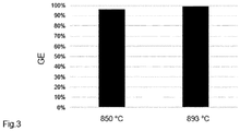
Fig. 3 shows the nickel getter efficiency (GE) for Examples 1 and 2.
The getter test consists of a reproducible spin-on contamination of the wafers with nickel, followed by a metal drive-in at 600 °C for 10 h under argon with a cooling rate of 3°C/min at the end. Then the metal profile on the wafer surface and near the wafer surface is evaluated by etching step by step using a mixture of hydrofluoric and nitric acid and subsequent analysis of the respective etching solutions by inductively coupled plasma mass spectrometry (ICPMS). -
Fig. 4 presents the results of LLS measurements on 50 test epitaxial semiconductor wafers, which have been thermally treated before epitaxial deposition according to Example 1. The results in terms of LLS having a size of more than 50 nm are similar to the results displayed inFig. 5 . -
Fig. 5 presents the results of LLS measurements on 50 test epitaxial semiconductor wafers, which have not been thermally treated before epitaxial deposition. For the LLS measurements a detection tool SP3 manufactured by KLA-Tencor Technologies Corporation was used in oblique incidence mode. -
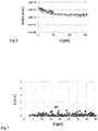
Fig. 6 shows the distribution of BMDs in depth direction to a depth d of about 150 µm (squares: Example 1, diamonds: Example 2). -
Fig. 7 shows for Example 1 the presence of dislocation loops in depth direction in terms the size (arbitrary units, a.u.) of etch pits. The presence of the dislocation loops is crucial for the gettering efficiency. The presence of a dislocation loop free zone near the interface between the epitaxial layer and the semiconductor wafer is crucial to prevent defects in the epi layer. -
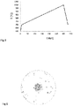
Fig. 8 shows the temperature ramps of the pre-epi heat treatment according to the Comparative Example. -
Fig. 9 represents a map displaying the positions of LLS on an epitaxial semiconductor wafer produced according to the Comparative Example. The inventors assume that the increased number of LLS is connected to the increased mean size of BMDs. - The above description of preferred embodiments has been given by way of example only. From the disclosure given, those skilled in the art will not only understand the present invention and its attendant advantages, but will also find apparent various changes and modifications to the structures and methods disclosed. The applicant seeks, therefore, to cover all such changes and modifications as fall within the spirit and scope of the invention, as defined by the appended claims, and equivalents thereof.
Claims (6)
- A semiconductor wafer made of single-crystal silicon with an oxygen concentration as per new ASTM of not less than 5.0 x 10¹⁷ atoms/ cm3 and of not more than 6.5 x 10¹⁷ atoms/cm3 and a nitrogen concentration as per new ASTM of not less than 1 x 10¹³ atoms/cm3 and not more than 1.0 x 10¹⁴ atoms/cm3, wherein a front side of the semiconductor wafer is covered with an epitaxial layer made of silicon, wherein the semiconductor wafer comprises BMDs whose mean size is not more than 10 nm determined by transmission electron microscopy and whose mean density in a region adjacent to the epitaxial layer is not less than 1.0 x 1011 cm-3, determined by reactive ion etching after having subjected the wafer covered with the epitaxial layer to a heat treatment at a temperature of 780 °C for a period of 3 h and to a heat treatment at a temperature of 600 °C for a period of 10 h.
- The wafer according to claim 1, wherein the semiconductor wafer has a nickel getter efficiency of at least 95%.
- The wafer according to any one of claims 1 and 2, wherein the mean density of BMDs decreases in the region adjacent to the epitaxial layer in depth direction.
- The wafer according to any one of claims 1 to 3, wherein dislocation loops are present in a region of the semiconductor wafer that is spaced apart from the interface between the epitaxial layer and the front side of the semiconductor wafer by not less than 2 µm and not more than 7 µm and that has a depth of at least 35 µm.
- The wafer according to any one of claims 1 to 4, wherein the oxygen concentration is not less than 5.7 x 10¹⁷ atoms/cm3 and not more than 6.2 x 10¹⁷ atoms/cm3.
- A process for producing a semiconductor wafer made of single-crystal silicon, comprising pulling a single crystal from a melt containing nitrogen according to the CZ method in an atmosphere comprising hydrogen, the partial pressure of hydrogen in the atmosphere being not less than 5 Pa and not more than 30 Pa, such that in a section of the single crystal having a uniform diameter the oxygen concentration is not less than 5.0 x 10¹⁷ atoms/ cm3 and not more than 6.5 x 10¹⁷ atoms/cm3, the nitrogen concentration is not less than 1.0 x 10¹³ atoms/cm3 and not more than 1.0 x 10¹⁴ atoms/ cm3;
controlling a pulling velocity V such that the single crystal in the section having a uniform diameter grows in a Pv region;
separating the semiconductor wafer from the section of the single crystal having a uniform diameter;
heat treating the semiconductor wafer from a temperature of not less than 600 °C to a target temperature of not more than 900 °C at a rate of not less than 0.5 °C/min and not more than 2°C/min;
cooling the semiconductor wafer from the target temperature to a temperature of not more than 600 °C at a rate of not less than 0.5 °C/min and not more than 2°C/min; and
depositing an epitaxial layer of silicon on a front side of the heat treated semiconductor wafer to form an epitaxial semiconductor wafer.
Priority Applications (9)
| Application Number | Priority Date | Filing Date | Title |
|---|---|---|---|
| EP20182286.3A EP3929335A1 (en) | 2020-06-25 | 2020-06-25 | Semiconductor wafer made of single-crystal silicon and process for the production thereof |
| US18/011,949 US12378692B2 (en) | 2020-06-25 | 2021-05-28 | Semiconductor wafer made of single-crystal silicon and process for the production thereof |
| PCT/EP2021/064323 WO2021259588A1 (en) | 2020-06-25 | 2021-05-28 | Semiconductor wafer made of single-crystal silicon and process for the production thereof |
| IL299255A IL299255A (en) | 2020-06-25 | 2021-05-28 | Semiconductor wafer made of single-crystal silicon and process for the production thereof |
| JP2022580181A JP7536903B2 (en) | 2020-06-25 | 2021-05-28 | Semiconductor wafer made from single crystal silicon and its manufacturing method |
| KR1020227045185A KR102754493B1 (en) | 2020-06-25 | 2021-05-28 | Semiconductor wafers made of single crystal silicon and their manufacturing process |
| CN202180044656.1A CN115715338A (en) | 2020-06-25 | 2021-05-28 | Semiconductor wafer made of monocrystalline silicon and method for producing the same |
| TW110123432A TWI807353B (en) | 2020-06-25 | 2021-06-25 | Semiconductor wafer made of single-crystal silicon and process for the production thereof |
| US19/214,282 US20250283249A1 (en) | 2020-06-25 | 2025-05-21 | Semiconductor wafer made of single-crystal silicon and process for the production thereof |
Applications Claiming Priority (1)
| Application Number | Priority Date | Filing Date | Title |
|---|---|---|---|
| EP20182286.3A EP3929335A1 (en) | 2020-06-25 | 2020-06-25 | Semiconductor wafer made of single-crystal silicon and process for the production thereof |
Publications (1)
| Publication Number | Publication Date |
|---|---|
| EP3929335A1 true EP3929335A1 (en) | 2021-12-29 |
Family
ID=71170292
Family Applications (1)
| Application Number | Title | Priority Date | Filing Date |
|---|---|---|---|
| EP20182286.3A Pending EP3929335A1 (en) | 2020-06-25 | 2020-06-25 | Semiconductor wafer made of single-crystal silicon and process for the production thereof |
Country Status (8)
| Country | Link |
|---|---|
| US (2) | US12378692B2 (en) |
| EP (1) | EP3929335A1 (en) |
| JP (1) | JP7536903B2 (en) |
| KR (1) | KR102754493B1 (en) |
| CN (1) | CN115715338A (en) |
| IL (1) | IL299255A (en) |
| TW (1) | TWI807353B (en) |
| WO (1) | WO2021259588A1 (en) |
Families Citing this family (1)
| Publication number | Priority date | Publication date | Assignee | Title |
|---|---|---|---|---|
| CN116005254A (en) * | 2022-12-26 | 2023-04-25 | 西安奕斯伟材料科技有限公司 | Epitaxial growth method and epitaxial silicon wafer |
Citations (6)
| Publication number | Priority date | Publication date | Assignee | Title |
|---|---|---|---|---|
| US20060150894A1 (en) | 2003-08-12 | 2006-07-13 | Shin-Etsu Handotai Co., Ltd. | Method for producing a wafer |
| US20070089666A1 (en) * | 2005-10-24 | 2007-04-26 | Yasuo Koike | Silicon semiconductor substrate and production method thereof |
| JP2007123543A (en) | 2005-10-27 | 2007-05-17 | Shin Etsu Handotai Co Ltd | Evaluation method of crystal defects |
| US20090210166A1 (en) * | 2004-01-27 | 2009-08-20 | Komatsu Denshi Kinzoku Kabushiki Kaisha | Method for predicting precipitation behavior of oxygen in silicon single crystal, method for determining production parameter of silicon single crystal, and storage medium for storing program for predicting precipitation behavior of oxygen in silicon single crystal |
| EP3394325A1 (en) * | 2015-12-22 | 2018-10-31 | Siltronic AG | Silicon wafer having a homogeneous radial oxygen variation |
| WO2019011638A1 (en) | 2017-07-10 | 2019-01-17 | Siltronic Ag | Semiconductor wafer made of single-crystal silicon and process for the production thereof |
Family Cites Families (9)
| Publication number | Priority date | Publication date | Assignee | Title |
|---|---|---|---|---|
| JPH1092761A (en) * | 1997-06-09 | 1998-04-10 | Sumitomo Sitix Corp | Manufacturing method of silicon wafer |
| JP3624827B2 (en) * | 2000-12-20 | 2005-03-02 | 三菱住友シリコン株式会社 | Method for producing silicon single crystal |
| JP2007123534A (en) | 2005-10-27 | 2007-05-17 | Sony Corp | Wiring pattern defect correcting method and defect correcting apparatus |
| DE102006055038B4 (en) * | 2006-11-22 | 2012-12-27 | Siltronic Ag | An epitaxated semiconductor wafer and apparatus and method for producing an epitaxied semiconductor wafer |
| JP5256195B2 (en) * | 2007-05-02 | 2013-08-07 | ジルトロニック アクチエンゲゼルシャフト | Silicon wafer and manufacturing method thereof |
| DE102008046617B4 (en) * | 2008-09-10 | 2016-02-04 | Siltronic Ag | Single crystal silicon wafer and process for its production |
| KR102384041B1 (en) * | 2014-07-31 | 2022-04-08 | 글로벌웨이퍼스 씨오., 엘티디. | Nitrogen doped and vacancy dominated silicon ingot and thermally treated wafer formed therefrom having radially uniformly distributed oxygen precipitation density and size |
| DE102015224983B4 (en) * | 2015-12-11 | 2019-01-24 | Siltronic Ag | Single crystal silicon wafer and process for its production |
| JP2018030765A (en) * | 2016-08-25 | 2018-03-01 | 信越半導体株式会社 | Silicon single crystal wafer manufacturing method, silicon epitaxial wafer manufacturing method, silicon single crystal wafer, and silicon epitaxial wafer |
-
2020
- 2020-06-25 EP EP20182286.3A patent/EP3929335A1/en active Pending
-
2021
- 2021-05-28 US US18/011,949 patent/US12378692B2/en active Active
- 2021-05-28 CN CN202180044656.1A patent/CN115715338A/en active Pending
- 2021-05-28 JP JP2022580181A patent/JP7536903B2/en active Active
- 2021-05-28 WO PCT/EP2021/064323 patent/WO2021259588A1/en not_active Ceased
- 2021-05-28 KR KR1020227045185A patent/KR102754493B1/en active Active
- 2021-05-28 IL IL299255A patent/IL299255A/en unknown
- 2021-06-25 TW TW110123432A patent/TWI807353B/en active
-
2025
- 2025-05-21 US US19/214,282 patent/US20250283249A1/en active Pending
Patent Citations (6)
| Publication number | Priority date | Publication date | Assignee | Title |
|---|---|---|---|---|
| US20060150894A1 (en) | 2003-08-12 | 2006-07-13 | Shin-Etsu Handotai Co., Ltd. | Method for producing a wafer |
| US20090210166A1 (en) * | 2004-01-27 | 2009-08-20 | Komatsu Denshi Kinzoku Kabushiki Kaisha | Method for predicting precipitation behavior of oxygen in silicon single crystal, method for determining production parameter of silicon single crystal, and storage medium for storing program for predicting precipitation behavior of oxygen in silicon single crystal |
| US20070089666A1 (en) * | 2005-10-24 | 2007-04-26 | Yasuo Koike | Silicon semiconductor substrate and production method thereof |
| JP2007123543A (en) | 2005-10-27 | 2007-05-17 | Shin Etsu Handotai Co Ltd | Evaluation method of crystal defects |
| EP3394325A1 (en) * | 2015-12-22 | 2018-10-31 | Siltronic AG | Silicon wafer having a homogeneous radial oxygen variation |
| WO2019011638A1 (en) | 2017-07-10 | 2019-01-17 | Siltronic Ag | Semiconductor wafer made of single-crystal silicon and process for the production thereof |
Also Published As
| Publication number | Publication date |
|---|---|
| JP7536903B2 (en) | 2024-08-20 |
| TWI807353B (en) | 2023-07-01 |
| TW202214917A (en) | 2022-04-16 |
| WO2021259588A1 (en) | 2021-12-30 |
| KR20230014759A (en) | 2023-01-30 |
| US12378692B2 (en) | 2025-08-05 |
| CN115715338A (en) | 2023-02-24 |
| US20250283249A1 (en) | 2025-09-11 |
| JP2023536220A (en) | 2023-08-24 |
| IL299255A (en) | 2023-02-01 |
| US20230235479A1 (en) | 2023-07-27 |
| KR102754493B1 (en) | 2025-01-13 |
Similar Documents
| Publication | Publication Date | Title |
|---|---|---|
| US7404856B2 (en) | Nitrogen-doped silicon substantially free of oxidation induced stacking faults | |
| JP6980893B2 (en) | Semiconductor wafers made from single crystal silicon and their manufacturing process | |
| CN101675507A (en) | Silicon wafer and method for manufacturing the same | |
| CN101024895A (en) | Epitaxial wafer and method for production of epitaxial wafer | |
| JP2015501533A (en) | Method for indicating the location of crystal related defects | |
| US20250283249A1 (en) | Semiconductor wafer made of single-crystal silicon and process for the production thereof | |
| JP4567251B2 (en) | Silicon semiconductor substrate and manufacturing method thereof | |
| US7071079B2 (en) | Epitaxial wafer and a method for producing it | |
| EP1536044A1 (en) | Silicon wafer for epitaxial growth, epitaxial wafer, and its manufacturing method | |
| JP4549589B2 (en) | Silicon semiconductor substrate and manufacturing method thereof | |
| US7396405B2 (en) | Single crystal, single crystal wafer, epitaxial wafer, and method of growing single crystal | |
| CN111279461B (en) | Semiconductor wafer composed of monocrystalline silicon | |
| WO2005053010A1 (en) | Annealed wafer and annealed wafer manufacturing method | |
| Abe et al. | A history and future of silicon crystal growth | |
| JP3731553B2 (en) | Evaluation method of nitrogen concentration in silicon wafer | |
| Abe | Isobe, Annaka, Gunma 379-0134, Japan | |
| Abe | the IC (integrated circuit) invention. Controls of dopants (BР) and light elements (CNO), elimination of heavy metals (Cu, Fe) have been done but a behavior of the point defects has |
Legal Events
| Date | Code | Title | Description |
|---|---|---|---|
| PUAI | Public reference made under article 153(3) epc to a published international application that has entered the european phase |
Free format text: ORIGINAL CODE: 0009012 |
|
| STAA | Information on the status of an ep patent application or granted ep patent |
Free format text: STATUS: THE APPLICATION HAS BEEN PUBLISHED |
|
| AK | Designated contracting states |
Kind code of ref document: A1 Designated state(s): AL AT BE BG CH CY CZ DE DK EE ES FI FR GB GR HR HU IE IS IT LI LT LU LV MC MK MT NL NO PL PT RO RS SE SI SK SM TR |
|
| B565 | Issuance of search results under rule 164(2) epc |
Effective date: 20210114 |
|
| STAA | Information on the status of an ep patent application or granted ep patent |
Free format text: STATUS: REQUEST FOR EXAMINATION WAS MADE |
|
| 17P | Request for examination filed |
Effective date: 20220214 |
|
| RBV | Designated contracting states (corrected) |
Designated state(s): AL AT BE BG CH CY CZ DE DK EE ES FI FR GB GR HR HU IE IS IT LI LT LU LV MC MK MT NL NO PL PT RO RS SE SI SK SM TR |
|
| STAA | Information on the status of an ep patent application or granted ep patent |
Free format text: STATUS: EXAMINATION IS IN PROGRESS |
|
| 17Q | First examination report despatched |
Effective date: 20240325 |