EP3923680B1 - Schaltung zum überbrücken von led-ketten - Google Patents
Schaltung zum überbrücken von led-ketten Download PDFInfo
- Publication number
- EP3923680B1 EP3923680B1 EP21178471.5A EP21178471A EP3923680B1 EP 3923680 B1 EP3923680 B1 EP 3923680B1 EP 21178471 A EP21178471 A EP 21178471A EP 3923680 B1 EP3923680 B1 EP 3923680B1
- Authority
- EP
- European Patent Office
- Prior art keywords
- effect transistor
- field effect
- source
- circuit
- light
- Prior art date
- Legal status (The legal status is an assumption and is not a legal conclusion. Google has not performed a legal analysis and makes no representation as to the accuracy of the status listed.)
- Active
Links
Images



Classifications
-
- H—ELECTRICITY
- H05—ELECTRIC TECHNIQUES NOT OTHERWISE PROVIDED FOR
- H05B—ELECTRIC HEATING; ELECTRIC LIGHT SOURCES NOT OTHERWISE PROVIDED FOR; CIRCUIT ARRANGEMENTS FOR ELECTRIC LIGHT SOURCES, IN GENERAL
- H05B45/00—Circuit arrangements for operating light-emitting diodes [LED]
- H05B45/10—Controlling the intensity of the light
-
- H—ELECTRICITY
- H05—ELECTRIC TECHNIQUES NOT OTHERWISE PROVIDED FOR
- H05B—ELECTRIC HEATING; ELECTRIC LIGHT SOURCES NOT OTHERWISE PROVIDED FOR; CIRCUIT ARRANGEMENTS FOR ELECTRIC LIGHT SOURCES, IN GENERAL
- H05B45/00—Circuit arrangements for operating light-emitting diodes [LED]
- H05B45/40—Details of LED load circuits
- H05B45/44—Details of LED load circuits with an active control inside an LED matrix
- H05B45/48—Details of LED load circuits with an active control inside an LED matrix having LEDs organised in strings and incorporating parallel shunting devices
-
- H—ELECTRICITY
- H05—ELECTRIC TECHNIQUES NOT OTHERWISE PROVIDED FOR
- H05B—ELECTRIC HEATING; ELECTRIC LIGHT SOURCES NOT OTHERWISE PROVIDED FOR; CIRCUIT ARRANGEMENTS FOR ELECTRIC LIGHT SOURCES, IN GENERAL
- H05B45/00—Circuit arrangements for operating light-emitting diodes [LED]
- H05B45/50—Circuit arrangements for operating light-emitting diodes [LED] responsive to malfunctions or undesirable behaviour of LEDs; responsive to LED life; Protective circuits
- H05B45/54—Circuit arrangements for operating light-emitting diodes [LED] responsive to malfunctions or undesirable behaviour of LEDs; responsive to LED life; Protective circuits in a series array of LEDs
Definitions
- the present invention relates to a circuit according to the preamble of claim 1.
- US 2018/338361 A1 concerns a light module.
- Another circuit for switching on and off at least one semiconductor light source which is arranged within a series circuit of first light-emitting diodes, represents an internal state of the art.
- a first end of the series circuit is connected to a working constant current source and a second end of the series circuit is connected to a ground terminal.
- a field effect transistor is electrically connected in parallel to the semiconductor light source.
- a source terminal of the field effect transistor is connected to a first terminal of the semiconductor light source.
- a drain terminal of the field effect transistor is connected to a second terminal of the semiconductor light source.
- a gate terminal of the field effect transistor is connected to a source terminal of the field effect transistor via a capacitor.
- the at least one semiconductor light source is, for example, a single LED or a chain, i.e. a series connection of several LEDs.
- Such series connections are used, for example, as light sources in lighting systems in motor vehicles.
- These light sources are generally operated with a pulse-width modulated signal that has a frequency of, for example, 100 Hz to 200 Hz.
- the light sources are switched on and off at this frequency, so that current phases and current pauses alternate.
- the human sense of sight perceives this as an average brightness, with the light sources appearing brighter the longer the current phases and the shorter the current pauses.
- the rapid switching on and off leads to steep edges in the current curve over time.
- the emission of interference radiation can occur, which can lead to a violation of electromagnetic compatibility (EMC) regulations.
- EMC electromagnetic compatibility
- the edge steepness can be reduced using the capacitor CGS2 of the known circuit.
- a disadvantage of this solution is that the setting range of this measure, i.e. the possible extent of the reduction in the edge steepness, is very limited.
- the object of the present invention is to provide a circuit of the type mentioned at the outset, which is characterized by an enlarged adjustment range and thus by improved electromagnetic compatibility.
- the control current source facilitates the adjustability of the edge slopes and charges the capacitor CGD1 with a constant current. This causes the gate source voltage of the field effect transistor to rise constantly.
- the parallel connection of the diode Ddischarge with the resistor R4 enables a different length of discharge compared to the charging of the MOSFET capacitors and the external capacitors.
- the additional capacitor CGD1 makes it possible to to make the critical edge when switching on the MOSFET, which is associated with a high current peak, flatter and to reduce the height of the current peak.
- the invention enables the use of larger output capacitors of a DC/DC converter as a control current source, which facilitates compliance with EMC guidelines.
- the invention enables smaller peak currents when bridging the LED chains, thus lower EMC interference, and fewer maximum current exceedances for the non-bridgeable LEDs.
- the invention makes it possible to bridge several LEDs at the same time, since maximum current values are maintained.
- the invention makes it possible to use Ddischarge and R4 to change the drain-source voltage change between drain and source and thus for the output capacitor of the DC/DC converter for the switch-off moment of the MOSFET. than for the switch-on moment via R6.
- the field effect transistor can switch to the desired high-impedance state more quickly.
- the invention is characterized in that a capacitor is connected in parallel to the working constant current source.
- the field effect transistor is a MOSFET, in particular an n-channel MOSFET.
- the semiconductor light source comprises an interconnection of several second light-emitting diodes.
- the interconnection comprises a series connection of several second light-emitting diodes.
- first light-emitting diodes and the second light-emitting diodes are the same.
- first light-emitting diodes are of a first type and the second light-emitting diodes are of a second type, the two types differing from one another. The difference is that the two types have different luminous fluxes emit.
- a further preferred embodiment is characterized in that the first light-emitting diodes are configured to emit light of a first light color and the second light-emitting diodes are configured to emit light of a second light color that differs from the first light color.
- a preferred use of the circuit is for switching on and off light-emitting diodes in lighting systems of motor vehicles.
- the Figure 1 a circuit 10 for switching on and off at least one semiconductor light source 12, which is arranged within a series circuit of light-emitting diodes.
- the semiconductor light source 12 is here a chain of LEDs D8, D9, D10, D11, D12, which in turn are connected in series.
- the chain forms the series circuit mentioned with the outer LEDs D7 and D13.
- a first end 14 of the series circuit is connected to an operating constant current source 16, and a second end 18 of the series circuit is connected to a ground connection 20.
- the operating constant current source 16 is preferably a DC/DC converter.
- An output capacitor C4 used for smoothing is connected in parallel to the operating constant current source 16.
- a field effect transistor 22 is electrically connected in parallel to the semiconductor light source 12.
- a source connection is source 2 of the field effect transistor 22 is connected to a first terminal 24 of the semiconductor light source 12, and a drain terminal Drain 2 of the field effect transistor 22 is connected to a second terminal 26 of the semiconductor light source 12.
- a gate terminal Gate2 of the field effect transistor 22 is connected via a capacitor CGS2 to the source terminal Source 2 of the field effect transistor 22 and via a resistor R2 to a control voltage source V1.
- the control voltage source outputs a control voltage uin.
- the switching speed with which the LEDs D8 to D12 of the semiconductor light source 12 are bridged depends on various field effect transistor-typical parameters, such as its total gate charge, its rise time and its full time.
- the current peak can in principle be reduced by specifically controlling the drain-source voltage of the field effect transistor 22 by reducing its switching speed.
- a capacitor CGS2 is installed between Gate2 and Source2.
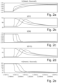
- the Figures 2a to 2e show qualitative curves of various quantities as they occur during operation of the circuit 10, each for three different values of the capacitor CG2. For each of the Figures 2a to 2e It is true that increasing the capacitance of the capacitor CGS2 reduces the steepness of the curves.
- Figure 2a shows the gate-source voltage over time.
- Figure 2b shows the current flowing through LED D7.
- Figure 2c shows the current flow through the LED D8, i.e. through the semiconductor light source 12, and
- Figure 2d shows the current flow through LED D13.
- Figure 2e shows the drain-source voltage of the field effect transistor 22.
- the capacitor CGS2 has the following technical effect: At the moment of switching, in which the LEDs D8 to D12 are bridged, the energy stored in the output capacitor C4 of the constant current source 16 is discharged.
- the capacitor CGS2 produces a change in the drain-source voltage of the field effect transistor 22 in a certain time. The current is limited by the output resistance of the field effect transistor 22. The slower the output resistance falls, i.e. the longer it remains high-resistance, the smaller the current peak.
- the increase in the output resistance of the MOSFET 22 can be slowed down, since the gate-source voltage increases more slowly due to the external capacitor CGS2, and thus the LED peak current reaches its peak value later.
- the maximum value of the LED current is always smaller with the external gate-source capacitance CGS2 than without it, which slows down the switching process in a desired way.
- a disadvantage of this solution is that the adjustment range of this measure, i.e. a possible extent of the reduction in the edge steepness, is very limited depending on the capacitance of the capacitor CGS2.
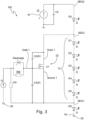
- Figure 3 shows an embodiment of the circuit 100 according to the invention with which the setting range of the switching speed of the MOSFET 22 is extended.
- a semiconductor light source 12 consisting of an LED chain, which is arranged within a series connection of light-emitting diodes.
- a first end SEG3 of the series connection is connected to a working constant current source 16, and a second end 18 of the Series connection is connected to a ground connection 20.
- a field effect transistor 22 is electrically connected in parallel to the semiconductor light source 12, wherein a source connection Source1 of the field effect transistor 22 is connected to a first connection SEG1 of the semiconductor light source 12, a drain connection Drain1 of the field effect transistor 22 is connected to a second connection SEG2 of the semiconductor light source 12 and a gate connection Gate1 of the field effect transistor 22 is connected to a control current source I2 and via a capacitor CGS1 to the source connection Source1 of the field effect transistor 22.
- the circuit 100 after the Figure 3 differs from circuit 10 according to the Figure 1 in that the drain connection Drain1 of the field effect transistor 22 in the circuit 100 is connected to the gate connection Gate1 of the field effect transistor 22 via a capacitor CGD1 and that the control current source I2 is connected to the gate connection Gate1 of the field effect transistor 22 via a parallel circuit comprising a diode Ddischarge and an ohmic resistor R6 and is connected to the source connection Source1 of the field effect transistor 22 via an ohmic resistor R4.
- the control current source I2 is preferably a constant current source.
- Fig. 4 shows a current (Ids) - voltage (Vds) - characteristic field of a MOSFET.
- the characteristic field shows a ohmic region 30 and a saturation region 32.
- the additional capacitor CGD1 according to the invention is electrically connected between the gate Gate1 and the drain Drain1 of the field effect transistor 22.
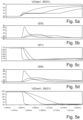
- FIGS. 5a to 5e show qualitative curves of various quantities as they occur during operation of the circuit, each for three different values of the capacitor CG2. For each of the figures, an increase in the capacitance of the capacitor CGS2 reduces the steepness of the curves.
- Figure 5a shows the gate-source voltage V(Gate1, SEG1) over time.
- Figure 5b shows the current flow through LED D0.
- Figure 5c shows the current through the LED D1, i.e. through the semiconductor light source 12 of the circuit 100, and
- Figure 2d shows the current flowing through LED D6.
- Figure 2e shows the drain-source voltage V(Drain1, SEG1).
- the courses are less close to each other in terms of time than the corresponding courses of the Figure 2 , which result without the capacitor CGD1.
- This stretching of the temporal courses of the Figure 5 compared to the temporal courses of the Figure 2 illustrates the desired increase in the adjustment range, which is achieved when using the circuit 100 according to the invention instead of the circuit 10 according to the Figure 1 results.
- Figure 6 shows known relationships between some field effect transistor parameters when switching on a field effect transistor.
- V stands for a voltage
- I for a current
- Q for a charge
- D for drain
- S for source
- G for gate
- pl for plateau
- th for threshold
- tot for total
- T for a point in time.
- the gate source capacitance of the field effect transistor 22 is charged up to the breakdown voltage V GS(th) .
- the drain source voltage V DS and the drain current I D do not change.
- the gate voltage V GS continues to increase up to the plateau.
- the Drain current I D increases to the maximum value.
- the gate source voltage remains at the Miller plateau V GS(pl) .
- control current source I2 promotes the widening of the adjustability and charges the capacitor CGD1 with a constant current. This causes the voltage V GS to rise constantly.
- the parallel connection of diode Ddischarge with resistor R4 allows a different length of discharge compared to the charging of the capacitances of the field effect transistor 22 and the external Capacitances CGD1 and CGS1, which occurs via the ohmic resistor R6.
- the additional capacitor CGD1 makes it possible to make the critical edge when switching on the field effect transistor 22, which is associated with a high current peak, less steep and to reduce the height of the current peak.
- a less steep MOSFET switch-on edge means that the ratio ⁇ u to ⁇ t (drain-source voltage change to ⁇ t) is reduced.
- the field effect transistor 22 is operated for longer in the ohmic region 30 of its characteristic field, whereby the height of the current peak is reduced as desired.
- the diode Ddischarge and the resistor R6 now make it possible to accelerate the non-critical edge when switching off the MOSFET and thus increase the drain-source voltage change. This reduces the power loss in the field effect transistor 22 and reduces the delay with which the field effect transistor 22 changes to the desired high-impedance state.
- One element of the invention is the constant current source I3 for constantly charging the capacitances of the field effect transistor 22 and the external capacitances.
- the invention enables the use of larger output capacitors (C2, C4) of the DC/DC converter serving as the working constant current source 16. This makes it easier to comply with EMC regulations.
- the invention also enables smaller peak currents at the moment of bridging the LED chains, thus lower EMC interference, and fewer maximum current exceedances for the non-bridgeable LEDs.
- the invention makes it possible to bridge several LEDs at the same time, since maximum current values are maintained.
- the invention makes it possible to use Ddischarge and R4 to design the drain-source voltage change between drain and source and thus for the output capacitor C4 of the working constant current source 16 for the turn-off process of the field effect transistor differently than for the turn-on process in which a charging current flows via the ohmic resistor R6.
- the field effect transistor 22 can change to the desired high-resistance state more quickly.
- the control constant current source I2 charges the capacitances of the field effect transistor 22 and also the external capacitors CGS1 and CGD1 via the ohmic resistor R6.
- the output resistance also increases more slowly due to the slower increase in the gate-source voltage and limits the current.
- the voltage from drain to source decreases more slowly. See the curve v(Drain-SEG1) in Figure 5e
- the discharge of the capacitor C2 becomes increasingly slower with increasing CGD1 and increasing CGS2.
- the field effect transistor 22 is switched off by discharging or recharging the internal capacitances through the diode Ddischarge and the resistor R4.
Landscapes
- Led Devices (AREA)
- Circuit Arrangement For Electric Light Sources In General (AREA)
Description
- Die vorliegende Erfindung betrifft eine Schaltung nach dem Oberbegriff des Anspruchs 1.
- Aus
DE 10 2015 204526 A1 ist bereits eine solche Schaltung bekannt. -
US 2018/338361 A1 betrifft ein Lichtmodul. - Eine weitere Schaltung zum Einschalten und Ausschalten von wenigstens einer Halbleiterlichtquelle, die innerhalb einer Reihenschaltung von ersten Leuchtdioden angeordnet ist, stellt einen internen Stand der Technik dar. Bei der bekannten Schaltung ist ein erstes Ende der Reihenschaltung an eine Arbeitskonstantstromquelle angeschlossen und ein zweites Ende der Reihenschaltung ist an einen Masseanschluss angeschlossen. Dabei ist ein Feldeffekttransistor elektrisch parallel zu der Halbleiterlichtquelle geschaltet. Ein Sourceanschluss des Feldeffekttransistors ist an einen ersten Anschluss der Halbleiterlichtquelle angeschlossen. Ein Drainanschluss des Feldeffekttransistors ist an einen zweiten Anschluss der Halbleiterlichtquelle angeschlossen. Ein Gateanschluss des Feldeffekttransistors ist über einen Kondensator an einen Sourceanschluss des Feldeffekttransistors angeschlossen.
- Darüber hinaus ist aus der
DE 10 2006 031 679 A1 eine Schaltungsanordnung zur elektrischen Ansteuerung eines Kraftfahrzeugscheinwerfers bekannt. - Bei der Schaltung des internen Standes der Technik ist die wenigstens eine Halbleiterlichtquelle zum Beispiel eine einzelne LED oder eine Kette, also eine Reihenschaltung von mehreren LEDs. Solche Reihenschaltungen werden zum Beispiel als Lichtquellen in Beleuchtungseinrichtungen von Kraftfahrzeugen verwendet. Diese Lichtquellen werden in der Regel mit einem pulsweitenmodulierten Signal betrieben, das eine Frequenz von zum Beispiel 100 Hz bis 200 Hz aufweist. Mit dieser Frequenz werden die Lichtquellen ein- und ausgeschaltet, so dass sich Stromphasen und Strompausen abwechseln. Der menschliche Sehsinn nimmt dies als eine mittlere Helligkeit wahr, wobei die Lichtquellen umso heller erscheinen, je länger die Stromphasen und je kürzer die Strompausen sind.
- Das schnelle Ein- und Ausschalten führt zu steilen Flanken im Stromverlauf über der Zeit. Als Folge kann eine Emission von Störstrahlung auftreten, die zur Verletzung von Vorschriften zur elektromagnetischen Verträglichkeit (EMV) führen kann. Mit dem Kondensator CGS2 der bekannten Schaltung kann die Flankensteilheit verringert werden. Ein Nachteil dieser Lösung besteht darin, dass ein Einstellbereich dieser Maßnahme, d.h. ein mögliches Ausmaß der Verringerung der Flankensteilheit sehr begrenzt ist.
- Vor diesem Hintergrund besteht die Aufgabe der vorliegenden Erfindung in der Angabe einer Schaltung der eingangs genannten Art, die sich durch einen vergrößerten Einstellbereich und damit durch eine verbesserte elektromagnetische Verträglichkeit auszeichnet.
- Diese Aufgabe wird mit den Merkmalen des Anspruchs 1 gelöst.
- Die Steuerstromquelle begünstigt die Einstellbarkeit der Flankensteigungen und lädt den Kondensator CGD1 mit konstantem Strom. Damit steigt die Gate Source Spannung des Feldeffekttransistors konstant an. Die Parallelschaltung der Diode Ddischarge mit dem Widerstand R4 ermöglicht ein unterschiedlich langes Entladen im Vergleich zum Laden der MOSFET-Kapazitäten und der externen Kapazitäten.
- Durch den zusätzlichen Kondensator CGD1 ist es möglich, die kritische Flanke beim Einschalten des MOSFET, die mit einem hohen Strompeak verbunden ist, flacher zu gestalten und die Höhe des Strompeaks zu reduzieren. Durch die Diode Ddischarge und den Widerstand R6 ist es nun möglich, die unkritische Flanke beim Abschalten des MOSFETs zu beschleunigen, die Drain-Source-Spannungsänderung zu vergrößern, um damit die Verlustleistung im Feldeffekttransistor zu reduzieren und die Verzögerung, mit der in den gewünschten hochohmigen Zustand gewechselt wird, zu verringern.
- Die Erfindung ermöglicht durch die Reduzierung der Entladeströme die Verwendung größerer Ausgangskondensatoren eines DC/DC-Wandlers als Steuerstromquelle, was die Einhaltung von EMV-Richtlinien erleichtert.
- Die Erfindung ermöglicht kleinere Spitzenströme beim Überbrücken der LED-Ketten, dadurch geringere EMV-Störgrößen, und weniger Maximalstromüberschreitungen für die nichtüberbrückbaren LEDs.
- Die Erfindung ermöglicht es, dass auch mehreren LEDs zur gleichen Zeit überbrückt werden können, da maximale Stromwerte eingehalten werden.
- Die Erfindung schafft die Möglichkeit, mit Ddischarge und R4 die Drain-Source-Spannungsänderung zwischen Drain und Source und damit für den Ausgangskondensator des DC/DC-Wandlers für den Ausschaltmoment des MOSFETS anders zu gestalten als für den Einschaltmoment über R6.
- Dadurch können die Verluste im Feldeffekttransistor reduziert werden, bei Beibehaltung der Stromspitzenunterdrückung, während des verlangsamten Einschaltens. Der Feldeffekttransistor kann schneller in den gewünschten hochohmigen Zustand wechseln.
- Die Erfindung zeichnet sich dadurch aus, dass der Arbeitskonstantstromquelle ein Kondensator parallel geschaltet ist.
- Bevorzugt ist es, wenn der Feldeffekttransistor ein MOSFET, insbesondere ein n-Kanal MOSFET ist.
- Erfindungsgemäß ist vorgesehen, dass die Halbleiterlichtquelle eine Zusammenschaltung von mehreren zweiten Leuchtdioden aufweist.
- Erfindungsgemäß weist die Zusammenschaltung eine Reihenschaltung von mehreren zweiten Leuchtdioden auf.
- Bevorzugt ist, dass die ersten Leuchtdioden und die zweiten Leuchtdioden gleich sind.
- Weiter ist bevorzugt, dass die ersten Leuchtdioden von einem ersten Typ sind und die zweiten Leuchtdioden von einem zweiten Typ sind, wobei sich die beiden Typen voneinander unterscheiden. Der Unterschied besteht darin, dass die beiden Typen unterschiedlich große Lichtströme emittieren.
- Eine weitere bevorzugte Ausgestaltung zeichnet sich dadurch aus, dass die ersten Leuchtdioden dazu eingerichtet sind, Licht einer ersten Lichtfarbe zu emittieren und die zweiten Leuchtdioden dazu eingerichtet sind, Licht einer zweiten Lichtfarbe zu emittieren, die sich von der ersten Lichtfarbe unterscheidet.
- Eine bevorzugte Verwendung der Schaltung erfolgt zum Einschalten und Ausschalten von Leuchtdioden in Beleuchtungseinrichtungen von Kraftfahrzeugen.
- Weitere Vorteile ergeben sich aus der nachfolgenden Beschreibung, den Zeichnungen und den Unteransprüchen. Es versteht sich, dass die vorstehend genannten und die nachstehend noch zu erläuternden Merkmale nicht nur in der jeweils angegebenen Kombination, sondern auch in anderen Kombinationen oder in Alleinstellung verwendbar sind, ohne den Rahmen der vorliegenden Erfindung zu verlassen.
- Ausführungsbeispiele der Erfindung sind in den Zeichnungen dargestellt und werden in der nachfolgenden Beschreibung näher erläutert.
- Dabei zeigen, jeweils in schematischer Form:
- Figur 1
- ein Schaltbild der Schaltung, die den internen Stand der Technik darstellt;
- Figur 2a
- Verläufe der Gate-Source-Spannung über der Zeit bei der Schaltung nach
Figur 1 ; - Figur 2b
- zeigt Verläufe des Stroms durch die LED D7 der
Figur 1 ; - Figur 2c
- Verläufe des Stroms durch die Halbleiterlichtquelle;
- Figur 2d
- Verläufe des Stroms durch die LED D13 der
Figur 1 ; - Figur 2e
- Verläufe der Drain-Source-Spannung des in der Schaltung nach
Figur 1 verwendeten MOSFETs; - Figur 3
- ein Ausführungsbeispiel der erfindungsgemäßen Schaltung;
- Figur 4
- ein Strom - Spannungs - Kennlinienfeld eines MOSFET;
- Figur 5a
- Verläufe der Gate-Source-Spannung in der Schaltung nach
Figur 1 über der Zeit; - Figur 5b
- Verläufe des Stroms durch die LED D7 der Schaltung nach
Figur 1 ; - Figur 5c
- Verläufe des Stroms durch die Halbleiterlichtquelle der Schaltung nach
Figur 1 ; - Figur 5d
- Verläufe des Stroms durch die LED D13 der Schaltung nach
Figur 1 ; - Figur 5e
- Verläufe der Drain-Source-Spannung des in der Schaltung nach
Figur 3 verwendeten MOSFETs; und - Figur 6
- an sich bekannte Zusammenhänge zwischen einigen Feldeffekttransistor Parametern beim Einschalten eines MOSFET.
- Im Einzelnen zeigt die
Figur 1 eine Schaltung 10 zum Einschalten und Ausschalten von wenigstens einer Halbleiterlichtquelle 12, die innerhalb einer Reihenschaltung von Leuchtdioden angeordnet ist. Die Halbleiterlichtquelle 12 ist hier eine Kette von LEDs D8, D9, D10, D11, D12, die ihrerseits in Reihe geschaltet sind. Die Kette bildet mit den äußeren LEDs D7 und D13 die genannte Reihenschaltung. Ein erstes Ende 14 der Reihenschaltung ist an eine Arbeitskonstantstromquelle 16 angeschlossen, und ein zweites Ende 18 der Reihenschaltung ist an einen Masseanschluss 20 angeschlossen. Die Arbeitskonstantstromquelle 16 ist bevorzugt ein DC/DC Wandler. Ein zur Glättung dienender Ausgangskondensator C4 ist parallel zu der Arbeitskonstantstromquelle 16 geschaltet. Ein Feldeffekttransistor 22 ist elektrisch parallel zu der Halbleiterlichtquelle 12 geschaltet. Dabei ist ein Sourceanschluss Source 2 des Feldeffekttransistors 22 an einen ersten Anschluss 24 der Halbleiterlichtquelle 12 angeschlossen, und ein Drainanschluss Drain 2 des Feldeffekttransistors 22 ist an einen zweiten Anschluss 26 der Halbleiterlichtquelle 12 angeschlossen. Ein Gateanschluss Gate2 des Feldeffekttransistors 22 ist über einen Kondensator CGS2 an den Sourceanschluss Source 2 des Feldeffekttransistors 22 und über einen Widerstand R2 an eine Steuerspannungsquelle V1 angeschlossen. Die Steuerspannungsquelle gibt eine Steuerspannung uin aus. - Die Schaltgeschwindigkeit, mit der die LEDs D8 bis D12 der Halbleiterlichtquelle 12 überbrückt werden, hängt von diversen Feldeffekttransistor-typischen Parametern ab, wie zum Beispielseiner Gesamt-Gate-Ladung, seiner Risetime und seiner Fulltime.
- Dadurch, dass, wie im Beispiel der
Figur 1 , mehrere LEDs D8 bis D12 zur gleichen Zeit überbrückt werden müssen, ist das Verhältnis der Drain-Source-Spannungsänderung Δu zur Änderungszeitspanne Δt sehr groß, was wiederum zu einer Stromspitze in den nicht geschalteten LEDs D7 und D13 inFigur 1 führt. Diese Stromspitze kann zum LED-Totalschaden oder einer Vorschädigung führen. - Die Stromspitze kann im Prinzip durch gezieltes Steuern der Drain-Source-Spannung des Feldeffekttransistors 22 reduziert werden, in dem dessen Schaltgeschwindigkeit verringert wird. Um die Schaltgeschwindigkeit des Feldeffekttransistors 22 zu verringern, wurde zum Beispiel bei einem n-Kanal Feldeffekttransistor 22 ein Kondensator CGS2 zwischen Gate2 und Source Source2 eingebaut. Ein Nachteil dieser Lösung ist, dass der Einstellbereich sehr begrenzt ist.
- Die
Figuren 2a bis 2e zeigen qualitativ Verläufe verschiedener Größen, wie sie beim Betrieb der Schaltung 10 auftreten, jeweils für drei verschiedene Werte des Kondensators CG2. Für jede derFiguren 2a bis 2e gilt, dass eine Vergrößerung der Kapazität des Kondensator CGS2 die Steilheit der Verläufe verringert. -
Figur 2a zeigt Verläufe der Gate-Source-Spannung über der Zeit.Figur 2b zeigt Verläufe des Stroms durch die LED D7.Figur 2c zeigt Verläufe des Stroms durch die LED D8, also durch die Halbleiterlichtquelle 12, undFigur 2d zeigt Verläufe des Stroms durch die LED D13.Figur 2e zeigt Verläufe der Drain-Source-Spannung des Feldeffekttransistors 22. - Wie man sieht, liegen die Verläufe in jeder Teilfigur noch relativ dicht beieinander, was ein Abbild eines relativ kleinen Einstellbereichs bei Änderungen der Kapazität des Kondensators CGS2 darstellt.
- Im Prinzip hat der Kondensator CGS2 den folgenden technischen Effekt: Im Moment des Umschaltens, in dem die LEDs D8 bis D12 überbrückt werden, wird die Energie, die im Ausgangskondensator C4 der Arbeitskonstantstromquelle 16 gespeichert ist, entladen. Am Kondensator CGS2 ergibt sich eine Änderung der Drain-Source-Spannung des Feldeffekttransistors 22 in einer bestimmten Zeit. Der Strom wird durch den Ausgangswiderstand des Feldeffekttransistors 22 begrenzt. Je langsamer der Ausgangswiderstand fällt, also je länger er hochohmig bleibt, umso kleiner ist die Stromspitze.
- Mit der zusätzlichen Kapazität CGS2 kann der Anstieg des Ausgangswiderstands des MOSFETs 22 verlangsamt werden, da die Gate-Source-Spannung durch den externen Kondensator CGS2 langsamer anwächst, und somit der LED-Spitzen-Strom später seinen Scheitelwert erreicht. Der maximale Wert des LED-Stroms ist mit der externen Gate-Source-Kapazität CGS2 immer kleiner als ohne, was den Ablauf des Schaltprozesses erwünscht verlangsamt. Wie bereits erwähnt, besteht ein Nachteil dieser Lösung darin, dass ein Einstellbereich dieser Maßnahme, d.h. ein mögliches Ausmaß der Verringerung der Flankensteilheit, in Abhängigkeit von der Kapazität des Kondensators CGS2 sehr begrenzt ist.
-
Figur 3 zeigt ein Ausführungsbeispiel der erfindungsgemäßen Schaltung 100 mit welcher der Einstellbereich der Schaltgeschwindigkeit des MOSFETs 22 erweitert wird. Im Einzelnen zeigt dieFigur 3 , wie auch schon dieFigur 1 , eine Halbleiterlichtquelle 12, bestehend aus einer LED-Kette, die innerhalb einer Reihenschaltung von Leuchtdioden angeordnet ist. Dabei ist ein erstes Ende SEG3 der Reihenschaltung an eine Arbeitskonstantstromquelle 16 angeschlossen, und ein zweites Ende 18 der Reihenschaltung ist an einen Masseanschluss 20 angeschlossen. Ein Feldeffekttransistor 22 ist elektrisch parallel zu der Halbleiterlichtquelle 12 geschaltet, wobei ein Sourceanschluss Source1 des Feldeffekttransistors 22 an einen ersten Anschluss SEG1 der Halbleiterlichtquelle 12 angeschlossen ist, ein Drainanschluss Drain1 des Feldeffekttransistors 22 an einen zweiten Anschluss SEG 2 der Halbleiterlichtquelle 12 angeschlossen ist und ein Gateanschluss Gate1 des Feldeffekttransistors 22 an eine Steuerstromquelle I2 und über einen Kondensator CGS1 an den Sourceanschluss Source1 des Feldeffekttransistors 22 angeschlossen ist. - Die Schaltung 100 nach der
Figur 3 unterscheidet sich von der Schaltung 10 nach derFigur 1 dadurch, dass der Drainanschluss Drain1 des Feldeffekttransistors 22 bei der Schaltung 100 über einen Kondensator CGD1 an den Gateanschluss Gate1 des Feldeffekttransistors 22 angeschlossen ist und dass die Steuerstromquelle I2 über eine Parallelschaltung aus einer Diode Ddischarge und einem ohmschen Widerstand R6 an den Gateanschluss Gate1 des Feldeffekttransistors 22 angeschlossen und über einen ohmschen Widerstand R4 an den Sourceanschluss Source1 des Feldeffekttransistors 22 angeschlossen ist. Die Steuerstromquelle I2 ist bevorzugt eine Konstantstromquelle. -
Fig. 4 zeigt ein Strom (Ids) - Spannungs (Vds) - Kennlinienfeld eines MOSFET. Das Kennlinienfeld weist einen ohmschen Bereich 30 und einen Sättigungsbereich 32 auf. Bei einem n-Kanal-MOSFET als Feldeffekttransistor 22 wird die Änderung der Spannung zwischen Gate und Source durch den weiteren Kondensator CGD1 während des Schaltvorgangs verlangsamt. Damit benötigt der Feldeffekttransistor mehr Zeit, um vom ohmschen Bereich 30 seiner Strom-Spannungs-Kennlinien in den gesättigten Bereich 32 zu wechseln. Je länger der Feldeffekttransistor 22 während des Schaltvorgangs im ohmschen Bereich 30 seiner Strom-Spannungs-Kennlinien bleibt, desto mehr im Ausgangskondensator C4 gespeicherte elektrische Energie wird im Feldeffekttransistor 22 in Wärme umgewandelt. Daraus ergibt sich die erwünschte Wirkung, dass der über den Feldeffekttransistor 22 und die LEDs D0 und D6 fließende Strom nicht ganz so hohe Werte erreicht wie es ohne den weiteren Kondensator CGD1 der Fall wäre. - Der erfindungsgemäß zusätzliche Kondensator CGD1 liegt elektrisch zwischen dem Gate Gate1 und dem Drain Drain1 des Feldeffekttransistors 22.
- Die
Figuren 5a bis 5e zeigen qualitativ Verläufe verschiedener Größen, wie sie beim Betrieb der Schaltung auftreten, jeweils für drei verschiedene Werte des Kondensators CG2. Für jede der Figuren gilt, dass eine Vergrößerung der Kapazität des Kondensators CGS2 die Steilheit der Verläufe verringert. -
Figur 5a zeigt Verläufe der Gate-Source-Spannung V(Gate1, SEG1) über der Zeit.Figur 5b zeigt Verläufe des Stroms durch die LED D0.Figur 5c zeigt Verläufe des Stroms durch die LED D1, also durch die Halbleiterlichtquelle 12 der Schaltung 100, undFigur 2d zeigt Verläufe des Stroms durch die LED D6.Figur 2e zeigt Verläufe der Drain-Source-Spannung V(Drain1, SEG1). - Wie man sieht, liegen die Verläufe in zeitlicher Hinsicht weniger dicht beieinander als die dazu korrespondierenden Verläufe der
Figur 2 , die sich ohne den Kondensator CGD1 ergeben. Diese Streckung der zeitlichen Verläufe derFigur 5 im Vergleich zu den zeitlichen Verläufen derFigur 2 verdeutlicht die erwünschte Vergrößerung des Einstellbereiches, die sich bei Verwendung der erfindungsgemäßen Schaltung 100 an Stelle der Schaltung 10 nach derFigur 1 ergibt. -
Figur 6 zeigt an sich bekannte Zusammenhänge zwischen einigen Feldeffekttransistor Parametern beim Einschalten eines Feldeffekttransistors. Dabei steht V für eine Spannung, I für einen Strom, Q für eine Ladung, D für Drain, S für Source, G für Gate, pl für Plateau, th für threshold, tot für total und T für einen Zeitpunkt. - In der Zeitspanne T1 - T0 wird die Gate Source Kapazität des Feldeffekttransistors 22 bis zur Durchbruchspannung VGS(th) geladen. Die Drain Source Spannung VDS und der Drain Strom ID ändern sich nicht. In der Zeitspanne T2 - T1 wächst die Gatespannung VGS weiter bis zum Plateau. Der Drain Strom ID wächst bis zum Maximalwert an. In der Zeitspanne T3 - T2 verharrt die Gate Source Spannung auf dem Millerplateu VGS(pl).
- Wie in
Figur 5a V(Gate1, SEG1) zu erkennen ist, steigt der am meisten rechts verlaufenden Verlauf langsamer an, als der am meisten links liegende Verlauf und der mittlere Verlauf. Der am meisten rechts liegende Verlauf ergibt sich aus dem größten CGD1. Durch die Maßnahme wird erreicht, dass nicht nur der Anstieg der Durchbruchspannung VGS(th) zur Plateauspannung VGS(pl) verzögert wird (sieheFigur 6 ), sondern dass durch die Verlängerung des Miller-Plateaus VGS(pl) die Drain Source Spannung VDS nicht so schnell abfallen kann. Damit reduziert sich die Spannung zwischen Drain Drain1 und Source Source1 über eine definierte Zeit. Die im parallel zur Arbeitskonstantstromquelle 16 liegenden Kondensator C2 gespeicherte Energie wird als Folge über einen verlängerten Zeitraum im Feldeffekttransistor 22 in Wärme umgewandelt. Der Stromanstieg ist daher reduziert. Die Fläche unter der Stromkurve bleibt konstant. - Die Verwendung einer Konstantstromquelle als Steuerstromquelle I2 begünstigt die Verbreiterung der Einstellbarkeit und lädt den Kondensator CGD1 mit konstantem Strom. Damit steigt die Spannung VGS konstant an. Die Parallelschaltung aus Diode Ddischarge mit dem Widerstand R4 (siehe
Figur 6 ) ermöglicht ein unterschiedlich langes Entladen im Vergleich zum Laden der Kapazitäten des Feldeffekttransistors 22 und der externen Kapazitäten CGD1 und CGS1, das über den ohmschen Widerstand R6 erfolgt. - Durch den zusätzlichen Kondensator CGD1 ist es möglich, die kritische Flanke beim Einschalten des Feldeffekttransistors 22, die mit einem hohen Strompeak verbunden ist, weniger steil zu gestalten und die Höhe des Strompeaks zu reduzieren. Eine weniger steile MOSFET-Einschaltflanke bedeutet, dass das Verhältnis Δu zu Δt (Drain-Source-Spannungsänderung zu Δt) verkleinert wird. Als Folge wird der Feldeffekttransistor 22 länger im ohmschen Bereich 30 seines Kennlinienfeldes betrieben, wodurch die Höhe des Strompeaks erwünscht reduziert wird. Durch die Diode Ddischarge und den Widerstand R6 ist es nun möglich, die unkritische Flanke beim Abschalten des MOSFETs zu beschleunigen und damit die Drain-Source-Spannungsänderung zu vergrößern. Damit wird die Verlustleistung im Feldeffekttransistor 22 reduziert, und die Verzögerung, mit welcher der Feldeffekttransistor 22 in den gewünschten hochohmigen Zustand wechselt, wird verringert.
- Ein Element der Erfindung ist die Konstantstromquelle I3 zum konstanten Laden der Kapazitäten des Feldeffekttransistors 22 und der externen Kapazitäten. Die Erfindung ermöglicht durch die Reduzierung der Entladeströme die Verwendung größerer Ausgangskondensatoren (C2, C4) des als Arbeitskonstantstromquelle 16 dienenden DC/DC-Wandlers. Dadurch können EMV-Vorschriften besser Richtlinien eingehalten werden.
- Die Erfindung ermöglicht weiter kleinere Spitzenströme im Moment der Überbrückung der LED-Ketten, dadurch geringere EMV-Störgrößen, und weniger Maximalstromüberschreitungen für die nichtüberbrückbaren LEDs.
- Die Erfindung ermöglicht es, dass auch mehrere LEDs zur gleichen Zeit überbrückt werden können, da maximale Stromwerte eingehalten werden.
- Die Erfindung schafft die Möglichkeit, mit Ddischarge und R4 die Drain-Source-Spannungsänderung zwischen Drain und Source und damit für den Ausgangskondensator C4 der Arbeitskonstantstromquelle 16 für den Ausschaltprozess des Feldeffekttransistors anders zu gestalten als für den Einschaltprozess, bei dem ein Ladestrom über den ohmschen Widerstand R6 fließt.
- Dadurch können die Verluste im Feldeffekttransistor 22 während des verlangsamten Einschaltens unter Beibehaltung der Stromspitzenunterdrückung reduziert werden. Der Feldeffekttransistor 22 kann schneller in den gewünschten hochohmigen Zustand wechseln.
- Die Steuerkonstantstromquelle I2 lädt während des Einschaltprozesses die Kapazitäten des Feldeffekttransistors 22 und auch die externen Kondensatoren CGS1 und CGD1 über den ohmschen Widerstand R6. Je größer CGD1 gewählt wird, umso mehr Zeit vergeht, bis die notwendige Gate-Source-Spannung für den leitenden Zustand aufgebaut ist. Siehe hierzu in der
Figur 5a den am meisten rechts liegenden Verlauf (größter CGD1) im Vergleich zum mittleren Verlauf (mittlerer CGD1) und zum am meisten links liegenden Verlauf (kleinster CGD1). Der Ausgangswiderstand steigt durch den verlangsamten Anstieg der Gate-Source-Spannung ebenso verlangsamt an und limitiert den Strom. Die Spannung von Drain nach Source fällt verlangsamt ab. Siehe hierzu den Kurvenverlauf v(Drain-SEG1) inFigur 5e . Die Entladung des Kondensators C2 erfolgt mit zunehmendem CGD1 und zunehmendem CGS2 zunehmend langsamer. - Das Abschalten des Feldeffekttransistors 22 erfolgt durch Entladen, bzw. Umladen der internen Kapazitäten durch die Diode Ddischarge und den Widerstand R4.
Claims (7)
- Schaltung (100) zum Einschalten und Ausschalten von wenigstens einer Halbleiterlichtquelle (12), die innerhalb einer Reihenschaltung von ersten Leuchtdioden (D0, D6) angeordnet ist, aufweisendeine Arbeitskonstantstromquelle (I2)einen Masseanschluss (20),ein Feldeffekttransistor(22),die wenigstens eine Halbleiterlichtquelle (12),die Reihenschaltung von ersten Leuchtdioden (D0, D6),einen Kondensator (CGD1)eine Diode (Ddischarge),ein Widerstand (R5),eine Steuerstromquelle (I3) einen weiteren Widerstand (R4) einen weiteren Kondensator (CGS1)einen dritten Kondensator (C2) wobei ein erstes Ende (SEG3) der Reihenschaltung an die Arbeitskonstantstromquelle (I2) angeschlossen ist und ein zweites Ende der Reihenschaltung an den Masseanschluss (20) angeschlossen ist, und wobei der Feldeffekttransistor (22) elektrisch parallel zu der wenigstens einen Halbleiterlichtquelle (12) geschaltet ist, wobei ein Sourceanschluss (Source1) des Feldeffekttransistors (22) an einen ersten Anschluss (SEG1) der wenigstens einen Halbleiterlichtquelle (12) angeschlossen ist, ein Drainanschluss (Drain1) des Feldeffekttransistors (22) an einen zweiten Anschluss (SEG2) der wenigstens einen Halbleiterlichtquelle (12) angeschlossen ist, wobei der Drainanschluss (Drain1) des Feldeffekttransistors (22) über den Kondensator (CGD1) an einen Gateanschluss (Gatel) des Feldeffekttransistors (22) angeschlossen ist,wobei die Diode (Ddischarge) und der Widerstand (R5) in einer Parallelschaltung parallel geschaltet sind und wobei die Steuerstromquelle (I3) über die Parallelschaltung an den Gateanschluss (Gatel) des Feldeffekttransistors (22) angeschlossen und über den weiteren Widerstand (R4) an den Sourceanschluss (Source1) des Feldeffekttransistors (22) angeschlossen ist,wobei die wenigstens eine Halbleiterlichtquelle (12) eine Zusammenschaltung von mehreren in Reihe geschalteten zweiten Leuchtdioden (D1, D2, D3, D4) aufweist,dadurch gekennzeichnet, dass der Gateanschluss (Gatel) des Feldeffekttransistors (22) über den weiteren Kondensator (CGS1) an den Sourceanschluss (Source1) des Feldeffekttransistors (22) angeschlossen ist,wobei der Arbeitskonstantstromquelle (16) der dritter Kondensator (C2) parallel geschaltet ist.
- Schaltung (100) nach Anspruch 1, wobei die Steuerstromquelle (I2) eine Konstantstromquelle ist.
- Schaltung (100) nach einem der vorhergehenden Ansprüche, wobei der Feldeffekttransistor (22) ein MOSFET ist.
- Schaltung (100) nach einem der Ansprüche 1 bis 3, wobei die ersten Leuchtdioden (D0, D6) und die zweiten Leuchtdioden (D1, D2, D3, D4, D5) gleich sind.
- Schaltung (100) nach einem der vorhergehenden Ansprüche, wobei die ersten Leuchtdioden (D0, D6) von einem ersten Typ sind und die zweiten Leuchtdioden (D1, D2, D3, D4, D5) von einem zweiten Typ sind, wobei sich die beiden Typen darin voneinander unterscheiden, dass die beiden Typen unterschiedlich große Lichtströme emittieren.
- Schaltung (100) nach Anspruch 5, wobei die ersten Leuchtdioden (D0, D6) dazu eingerichtet sind, Licht einer ersten Lichtfarbe zu emittieren und die zweiten Leuchtdioden (D1, D2, D3, D4, D5) dazu eingerichtet sind, Licht einer zweiten Lichtfarbe zu emittieren, die sich von der ersten Lichtfarbe unterscheidet.
- Verwendung einer Schaltung (100) nach Anspruch 1 zum Einschalten und Ausschalten von Leuchtdioden in Beleuchtungseinrichtungen von Kraftfahrzeugen.
Applications Claiming Priority (1)
| Application Number | Priority Date | Filing Date | Title |
|---|---|---|---|
| DE102020115437.2A DE102020115437A1 (de) | 2020-06-10 | 2020-06-10 | Schaltung zum Überbrücken von LED-Ketten |
Publications (2)
| Publication Number | Publication Date |
|---|---|
| EP3923680A1 EP3923680A1 (de) | 2021-12-15 |
| EP3923680B1 true EP3923680B1 (de) | 2025-01-01 |
Family
ID=76355367
Family Applications (1)
| Application Number | Title | Priority Date | Filing Date |
|---|---|---|---|
| EP21178471.5A Active EP3923680B1 (de) | 2020-06-10 | 2021-06-09 | Schaltung zum überbrücken von led-ketten |
Country Status (2)
| Country | Link |
|---|---|
| EP (1) | EP3923680B1 (de) |
| DE (1) | DE102020115437A1 (de) |
Citations (2)
| Publication number | Priority date | Publication date | Assignee | Title |
|---|---|---|---|---|
| US9781789B1 (en) * | 2016-05-13 | 2017-10-03 | Allegro Microsystems, Llc | Apparatus and methods for LED control |
| US20180098392A1 (en) * | 2016-09-30 | 2018-04-05 | Once, Inc. | Dimmable analog ac circuit |
Family Cites Families (4)
| Publication number | Priority date | Publication date | Assignee | Title |
|---|---|---|---|---|
| DE102006031679A1 (de) | 2006-07-08 | 2008-01-10 | Hella Kgaa Hueck & Co. | Schaltungsanordnung zur elektrischen Ansteuerung eines Kraftfahrzeug-Scheinwerfers |
| FR3018659B1 (fr) * | 2014-03-14 | 2020-03-27 | Koito Manufacturing Co., Ltd. | Lampe pour vehicule et dispositif de commande de lampe pour vehicule |
| DE202017100741U1 (de) * | 2017-02-13 | 2017-02-22 | Automotive Lighting Reutlingen Gmbh | Schaltungsanordnung einer Beleuchtungseinrichtung mit elektrischer Lastanordnung |
| FR3066674B1 (fr) * | 2017-05-19 | 2021-09-03 | Valeo Vision | Source de courant partagee par plusieurs emetteurs de lumiere |
-
2020
- 2020-06-10 DE DE102020115437.2A patent/DE102020115437A1/de active Pending
-
2021
- 2021-06-09 EP EP21178471.5A patent/EP3923680B1/de active Active
Patent Citations (2)
| Publication number | Priority date | Publication date | Assignee | Title |
|---|---|---|---|---|
| US9781789B1 (en) * | 2016-05-13 | 2017-10-03 | Allegro Microsystems, Llc | Apparatus and methods for LED control |
| US20180098392A1 (en) * | 2016-09-30 | 2018-04-05 | Once, Inc. | Dimmable analog ac circuit |
Non-Patent Citations (2)
| Title |
|---|
| LASZLO BALOGH: "Fundamentals of MOSFET and IGBT Gate Driver Circuits, Application Report SLUA618A", 15 October 2018 (2018-10-15), Dallas, Texas, USA, pages 1 - 48, XP055622268, Retrieved from the Internet <URL:http://www.ti.com/lit/ml/slua618a/slua618a.pdf> [retrieved on 20190913] * |
| YIN SHAN ET AL: "An Accurate Subcircuit Model of SiC Half-Bridge Module for Switching-Loss Optimization", IEEE TRANSACTIONS ON INDUSTRY APPLICATIONS, IEEE SERVICE CENTER, PISCATAWAY, NJ, US, vol. 53, no. 4, 1 July 2017 (2017-07-01), pages 3840 - 3848, XP011656794, ISSN: 0093-9994, [retrieved on 20170717], DOI: 10.1109/TIA.2017.2691734 * |
Also Published As
| Publication number | Publication date |
|---|---|
| DE102020115437A1 (de) | 2021-12-16 |
| EP3923680A1 (de) | 2021-12-15 |
Similar Documents
| Publication | Publication Date | Title |
|---|---|---|
| DE19841490B4 (de) | Schaltungsanordnung zum Schutz einer Serienschaltung aus mindestens zwei Leuchdioden vor dem Ausfall | |
| DE19902520A1 (de) | Hybrid-Leistungs-MOSFET | |
| EP2683221A1 (de) | Anordnung und Verfahren zur Ansteuerung von Leuchtdioden in abhängigkeit vom Eingangsspannungs-pegel, mittels Kondensator und Schalter | |
| DE102015204526A1 (de) | Fahrzeuglampe und Fahrzeuglampenansteuervorrichtung | |
| DE3904901A1 (de) | Integrierte gegentakt-ausgangsstufe | |
| DE60313733T2 (de) | Ansteuerschaltung für einen Steueranschluss eines Bipolartransistors, der in der Emitterschattkonfiguration ist und entsprechenes Ansteuerverfahren | |
| DE102005038231B3 (de) | Verfahren und Vorrichtung zum Einschalten einer Spannungsversorgung einer Halbleiterschaltung und entsprechende Halbleiterschaltung | |
| DE102012223816B3 (de) | Einrichtung zur Ansteuerung eines Feldeffekttransistors | |
| DE19527736C1 (de) | Schaltungsanordnung zur Ansteuerung eines dem Speisekreis einer elektrischen Last zugeordneten MOS-Feldeffekttransistors | |
| WO2014114486A2 (de) | Anordnung und verfahren zum betreiben einer anordnung | |
| EP1094605B1 (de) | Schaltungsanordnung zum Ansteuern einer Last mit reduzierter Störabstrahlung | |
| DE102005027442B4 (de) | Schaltungsanordnung zum Schalten einer Last | |
| DE112013001483T5 (de) | LED-Beleuchtungseinrichtung | |
| DE10236872A1 (de) | Schaltungsanordnung zur steuerbaren Stromversorgung, insbesondere Schaltungsanordnung zum Dimmen von Leuchtdiodenanordnungen | |
| EP3923680A1 (de) | Schaltung zum überbrücken von led-ketten | |
| DE102011055122A1 (de) | Widerstandsschaltung, Schaltungsanordnung und Treiber | |
| DE3230080A1 (de) | Steueranordnung fuer impulsgesteuerte feldeffekttransistoren | |
| DE102013221753A1 (de) | Schaltungsanordnung, Leuchtdioden-Anordnung und Verfahren zum Ansteuern eines optoelektronischen Bauelements | |
| WO2020109291A1 (de) | Leistungsschalteranordnung | |
| DE102016223312A1 (de) | Leistungshalbleiterbaugruppe für ein Kraftfahrzeug, Kraftfahrzeug und Verfahren zum Betreiben einer Leistungshalbleiterbaugruppe | |
| EP3163979B1 (de) | Ein lichtmodul und ein verfahren zum betreiben eines lichtmoduls | |
| DE202017100741U1 (de) | Schaltungsanordnung einer Beleuchtungseinrichtung mit elektrischer Lastanordnung | |
| EP3125651A1 (de) | Dimmen von beleuchtungsvorrichtungen | |
| DE102015206031A1 (de) | Vorrichtung zum Begrenzen einer über einem Leistungsschalter abfallenden Spannung, Spannungszwischenkreisumrichter sowie Verfahren | |
| DE102006043900B4 (de) | Vorrichtung und Verfahren zum Betrieb einer Plasmaanlage |
Legal Events
| Date | Code | Title | Description |
|---|---|---|---|
| PUAI | Public reference made under article 153(3) epc to a published international application that has entered the european phase |
Free format text: ORIGINAL CODE: 0009012 |
|
| STAA | Information on the status of an ep patent application or granted ep patent |
Free format text: STATUS: THE APPLICATION HAS BEEN PUBLISHED |
|
| AK | Designated contracting states |
Kind code of ref document: A1 Designated state(s): AL AT BE BG CH CY CZ DE DK EE ES FI FR GB GR HR HU IE IS IT LI LT LU LV MC MK MT NL NO PL PT RO RS SE SI SK SM TR |
|
| B565 | Issuance of search results under rule 164(2) epc |
Effective date: 20211001 |
|
| STAA | Information on the status of an ep patent application or granted ep patent |
Free format text: STATUS: REQUEST FOR EXAMINATION WAS MADE |
|
| 17P | Request for examination filed |
Effective date: 20220523 |
|
| RBV | Designated contracting states (corrected) |
Designated state(s): AL AT BE BG CH CY CZ DE DK EE ES FI FR GB GR HR HU IE IS IT LI LT LU LV MC MK MT NL NO PL PT RO RS SE SI SK SM TR |
|
| STAA | Information on the status of an ep patent application or granted ep patent |
Free format text: STATUS: EXAMINATION IS IN PROGRESS |
|
| 17Q | First examination report despatched |
Effective date: 20230405 |
|
| GRAP | Despatch of communication of intention to grant a patent |
Free format text: ORIGINAL CODE: EPIDOSNIGR1 |
|
| STAA | Information on the status of an ep patent application or granted ep patent |
Free format text: STATUS: GRANT OF PATENT IS INTENDED |
|
| INTG | Intention to grant announced |
Effective date: 20240723 |
|
| GRAS | Grant fee paid |
Free format text: ORIGINAL CODE: EPIDOSNIGR3 |
|
| GRAA | (expected) grant |
Free format text: ORIGINAL CODE: 0009210 |
|
| STAA | Information on the status of an ep patent application or granted ep patent |
Free format text: STATUS: THE PATENT HAS BEEN GRANTED |
|
| AK | Designated contracting states |
Kind code of ref document: B1 Designated state(s): AL AT BE BG CH CY CZ DE DK EE ES FI FR GB GR HR HU IE IS IT LI LT LU LV MC MK MT NL NO PL PT RO RS SE SI SK SM TR |
|
| RAP3 | Party data changed (applicant data changed or rights of an application transferred) |
Owner name: MARELLI GERMANY GMBH |
|
| REG | Reference to a national code |
Ref country code: GB Ref legal event code: FG4D Free format text: NOT ENGLISH |
|
| P01 | Opt-out of the competence of the unified patent court (upc) registered |
Free format text: CASE NUMBER: APP_64189/2024 Effective date: 20241204 |
|
| REG | Reference to a national code |
Ref country code: DE Ref legal event code: R096 Ref document number: 502021006244 Country of ref document: DE |
|
| REG | Reference to a national code |
Ref country code: CH Ref legal event code: EP |
|
| REG | Reference to a national code |
Ref country code: IE Ref legal event code: FG4D Free format text: LANGUAGE OF EP DOCUMENT: GERMAN |
|
| REG | Reference to a national code |
Ref country code: LT Ref legal event code: MG9D |
|
| REG | Reference to a national code |
Ref country code: NL Ref legal event code: MP Effective date: 20250101 |
|
| PG25 | Lapsed in a contracting state [announced via postgrant information from national office to epo] |
Ref country code: NL Free format text: LAPSE BECAUSE OF FAILURE TO SUBMIT A TRANSLATION OF THE DESCRIPTION OR TO PAY THE FEE WITHIN THE PRESCRIBED TIME-LIMIT Effective date: 20250101 |
|
| PG25 | Lapsed in a contracting state [announced via postgrant information from national office to epo] |
Ref country code: FI Free format text: LAPSE BECAUSE OF FAILURE TO SUBMIT A TRANSLATION OF THE DESCRIPTION OR TO PAY THE FEE WITHIN THE PRESCRIBED TIME-LIMIT Effective date: 20250101 |
|
| PG25 | Lapsed in a contracting state [announced via postgrant information from national office to epo] |
Ref country code: PL Free format text: LAPSE BECAUSE OF FAILURE TO SUBMIT A TRANSLATION OF THE DESCRIPTION OR TO PAY THE FEE WITHIN THE PRESCRIBED TIME-LIMIT Effective date: 20250101 |
|
| PGFP | Annual fee paid to national office [announced via postgrant information from national office to epo] |
Ref country code: DE Payment date: 20250520 Year of fee payment: 5 |
|
| PG25 | Lapsed in a contracting state [announced via postgrant information from national office to epo] |
Ref country code: ES Free format text: LAPSE BECAUSE OF FAILURE TO SUBMIT A TRANSLATION OF THE DESCRIPTION OR TO PAY THE FEE WITHIN THE PRESCRIBED TIME-LIMIT Effective date: 20250101 |
|
| PG25 | Lapsed in a contracting state [announced via postgrant information from national office to epo] |
Ref country code: NO Free format text: LAPSE BECAUSE OF FAILURE TO SUBMIT A TRANSLATION OF THE DESCRIPTION OR TO PAY THE FEE WITHIN THE PRESCRIBED TIME-LIMIT Effective date: 20250401 Ref country code: IS Free format text: LAPSE BECAUSE OF FAILURE TO SUBMIT A TRANSLATION OF THE DESCRIPTION OR TO PAY THE FEE WITHIN THE PRESCRIBED TIME-LIMIT Effective date: 20250501 |
|
| PG25 | Lapsed in a contracting state [announced via postgrant information from national office to epo] |
Ref country code: HR Free format text: LAPSE BECAUSE OF FAILURE TO SUBMIT A TRANSLATION OF THE DESCRIPTION OR TO PAY THE FEE WITHIN THE PRESCRIBED TIME-LIMIT Effective date: 20250101 |
|
| PG25 | Lapsed in a contracting state [announced via postgrant information from national office to epo] |
Ref country code: LV Free format text: LAPSE BECAUSE OF FAILURE TO SUBMIT A TRANSLATION OF THE DESCRIPTION OR TO PAY THE FEE WITHIN THE PRESCRIBED TIME-LIMIT Effective date: 20250101 Ref country code: PT Free format text: LAPSE BECAUSE OF FAILURE TO SUBMIT A TRANSLATION OF THE DESCRIPTION OR TO PAY THE FEE WITHIN THE PRESCRIBED TIME-LIMIT Effective date: 20250502 |
|
| PG25 | Lapsed in a contracting state [announced via postgrant information from national office to epo] |
Ref country code: BG Free format text: LAPSE BECAUSE OF FAILURE TO SUBMIT A TRANSLATION OF THE DESCRIPTION OR TO PAY THE FEE WITHIN THE PRESCRIBED TIME-LIMIT Effective date: 20250101 Ref country code: GR Free format text: LAPSE BECAUSE OF FAILURE TO SUBMIT A TRANSLATION OF THE DESCRIPTION OR TO PAY THE FEE WITHIN THE PRESCRIBED TIME-LIMIT Effective date: 20250402 |
|
| PGFP | Annual fee paid to national office [announced via postgrant information from national office to epo] |
Ref country code: AT Payment date: 20250721 Year of fee payment: 5 |
|
| PG25 | Lapsed in a contracting state [announced via postgrant information from national office to epo] |
Ref country code: CZ Free format text: LAPSE BECAUSE OF FAILURE TO SUBMIT A TRANSLATION OF THE DESCRIPTION OR TO PAY THE FEE WITHIN THE PRESCRIBED TIME-LIMIT Effective date: 20250101 |
|
| PG25 | Lapsed in a contracting state [announced via postgrant information from national office to epo] |
Ref country code: SE Free format text: LAPSE BECAUSE OF FAILURE TO SUBMIT A TRANSLATION OF THE DESCRIPTION OR TO PAY THE FEE WITHIN THE PRESCRIBED TIME-LIMIT Effective date: 20250101 |
|
| REG | Reference to a national code |
Ref country code: DE Ref legal event code: R097 Ref document number: 502021006244 Country of ref document: DE |
|
| PG25 | Lapsed in a contracting state [announced via postgrant information from national office to epo] |
Ref country code: SM Free format text: LAPSE BECAUSE OF FAILURE TO SUBMIT A TRANSLATION OF THE DESCRIPTION OR TO PAY THE FEE WITHIN THE PRESCRIBED TIME-LIMIT Effective date: 20250101 |
|
| PG25 | Lapsed in a contracting state [announced via postgrant information from national office to epo] |
Ref country code: DK Free format text: LAPSE BECAUSE OF FAILURE TO SUBMIT A TRANSLATION OF THE DESCRIPTION OR TO PAY THE FEE WITHIN THE PRESCRIBED TIME-LIMIT Effective date: 20250101 |
|
| PG25 | Lapsed in a contracting state [announced via postgrant information from national office to epo] |
Ref country code: IT Free format text: LAPSE BECAUSE OF FAILURE TO SUBMIT A TRANSLATION OF THE DESCRIPTION OR TO PAY THE FEE WITHIN THE PRESCRIBED TIME-LIMIT Effective date: 20250101 |
|
| PG25 | Lapsed in a contracting state [announced via postgrant information from national office to epo] |
Ref country code: EE Free format text: LAPSE BECAUSE OF FAILURE TO SUBMIT A TRANSLATION OF THE DESCRIPTION OR TO PAY THE FEE WITHIN THE PRESCRIBED TIME-LIMIT Effective date: 20250101 |
|
| PG25 | Lapsed in a contracting state [announced via postgrant information from national office to epo] |
Ref country code: RO Free format text: LAPSE BECAUSE OF FAILURE TO SUBMIT A TRANSLATION OF THE DESCRIPTION OR TO PAY THE FEE WITHIN THE PRESCRIBED TIME-LIMIT Effective date: 20250101 |
|
| PG25 | Lapsed in a contracting state [announced via postgrant information from national office to epo] |
Ref country code: SK Free format text: LAPSE BECAUSE OF FAILURE TO SUBMIT A TRANSLATION OF THE DESCRIPTION OR TO PAY THE FEE WITHIN THE PRESCRIBED TIME-LIMIT Effective date: 20250101 |
|
| PLBE | No opposition filed within time limit |
Free format text: ORIGINAL CODE: 0009261 |
|
| STAA | Information on the status of an ep patent application or granted ep patent |
Free format text: STATUS: NO OPPOSITION FILED WITHIN TIME LIMIT |
|
| REG | Reference to a national code |
Ref country code: CH Ref legal event code: L10 Free format text: ST27 STATUS EVENT CODE: U-0-0-L10-L00 (AS PROVIDED BY THE NATIONAL OFFICE) Effective date: 20251112 |
|
| 26N | No opposition filed |
Effective date: 20251002 |
|
| REG | Reference to a national code |
Ref country code: CH Ref legal event code: H13 Free format text: ST27 STATUS EVENT CODE: U-0-0-H10-H13 (AS PROVIDED BY THE NATIONAL OFFICE) Effective date: 20260127 |
|
| PG25 | Lapsed in a contracting state [announced via postgrant information from national office to epo] |
Ref country code: MC Free format text: LAPSE BECAUSE OF FAILURE TO SUBMIT A TRANSLATION OF THE DESCRIPTION OR TO PAY THE FEE WITHIN THE PRESCRIBED TIME-LIMIT Effective date: 20250101 |
|
| PG25 | Lapsed in a contracting state [announced via postgrant information from national office to epo] |
Ref country code: LU Free format text: LAPSE BECAUSE OF NON-PAYMENT OF DUE FEES Effective date: 20250609 |
|
| GBPC | Gb: european patent ceased through non-payment of renewal fee |
Effective date: 20250609 |
|
| REG | Reference to a national code |
Ref country code: BE Ref legal event code: MM Effective date: 20250630 |
|
| PG25 | Lapsed in a contracting state [announced via postgrant information from national office to epo] |
Ref country code: GB Free format text: LAPSE BECAUSE OF NON-PAYMENT OF DUE FEES Effective date: 20250609 |
|
| PG25 | Lapsed in a contracting state [announced via postgrant information from national office to epo] |
Ref country code: IE Free format text: LAPSE BECAUSE OF NON-PAYMENT OF DUE FEES Effective date: 20250609 |
|
| PG25 | Lapsed in a contracting state [announced via postgrant information from national office to epo] |
Ref country code: BE Free format text: LAPSE BECAUSE OF NON-PAYMENT OF DUE FEES Effective date: 20250630 |
|
| PG25 | Lapsed in a contracting state [announced via postgrant information from national office to epo] |
Ref country code: FR Free format text: LAPSE BECAUSE OF NON-PAYMENT OF DUE FEES Effective date: 20250630 |
|
| PG25 | Lapsed in a contracting state [announced via postgrant information from national office to epo] |
Ref country code: CH Free format text: LAPSE BECAUSE OF NON-PAYMENT OF DUE FEES Effective date: 20250630 |