US20180098392A1 - Dimmable analog ac circuit - Google Patents
Dimmable analog ac circuit Download PDFInfo
- Publication number
- US20180098392A1 US20180098392A1 US15/680,980 US201715680980A US2018098392A1 US 20180098392 A1 US20180098392 A1 US 20180098392A1 US 201715680980 A US201715680980 A US 201715680980A US 2018098392 A1 US2018098392 A1 US 2018098392A1
- Authority
- US
- United States
- Prior art keywords
- voltage
- transistor
- led group
- current
- circuit
- Prior art date
- Legal status (The legal status is an assumption and is not a legal conclusion. Google has not performed a legal analysis and makes no representation as to the accuracy of the status listed.)
- Granted
Links
- 239000003990 capacitor Substances 0.000 claims abstract description 14
- 230000003750 conditioning effect Effects 0.000 description 17
- 238000010586 diagram Methods 0.000 description 10
- 230000009471 action Effects 0.000 description 8
- 238000005516 engineering process Methods 0.000 description 8
- 238000000034 method Methods 0.000 description 6
- 241001465754 Metazoa Species 0.000 description 5
- 230000001419 dependent effect Effects 0.000 description 4
- 230000005669 field effect Effects 0.000 description 4
- 230000006870 function Effects 0.000 description 4
- 239000004065 semiconductor Substances 0.000 description 4
- 230000007704 transition Effects 0.000 description 4
- 230000007423 decrease Effects 0.000 description 3
- 229910000577 Silicon-germanium Inorganic materials 0.000 description 2
- 238000013459 approach Methods 0.000 description 2
- 230000008901 benefit Effects 0.000 description 2
- 239000003086 colorant Substances 0.000 description 2
- 238000013461 design Methods 0.000 description 2
- 230000012010 growth Effects 0.000 description 2
- 238000012986 modification Methods 0.000 description 2
- 230000004048 modification Effects 0.000 description 2
- 230000008635 plant growth Effects 0.000 description 2
- 230000008569 process Effects 0.000 description 2
- 239000000758 substrate Substances 0.000 description 2
- JBRZTFJDHDCESZ-UHFFFAOYSA-N AsGa Chemical compound [As]#[Ga] JBRZTFJDHDCESZ-UHFFFAOYSA-N 0.000 description 1
- 229910005540 GaP Inorganic materials 0.000 description 1
- GPXJNWSHGFTCBW-UHFFFAOYSA-N Indium phosphide Chemical compound [In]#P GPXJNWSHGFTCBW-UHFFFAOYSA-N 0.000 description 1
- LEVVHYCKPQWKOP-UHFFFAOYSA-N [Si].[Ge] Chemical compound [Si].[Ge] LEVVHYCKPQWKOP-UHFFFAOYSA-N 0.000 description 1
- 230000003213 activating effect Effects 0.000 description 1
- 230000004913 activation Effects 0.000 description 1
- 230000009286 beneficial effect Effects 0.000 description 1
- 239000002800 charge carrier Substances 0.000 description 1
- 238000001514 detection method Methods 0.000 description 1
- 238000007599 discharging Methods 0.000 description 1
- 230000000694 effects Effects 0.000 description 1
- 230000005684 electric field Effects 0.000 description 1
- HZXMRANICFIONG-UHFFFAOYSA-N gallium phosphide Chemical compound [Ga]#P HZXMRANICFIONG-UHFFFAOYSA-N 0.000 description 1
- 238000003898 horticulture Methods 0.000 description 1
- 229910052738 indium Inorganic materials 0.000 description 1
- APFVFJFRJDLVQX-UHFFFAOYSA-N indium atom Chemical compound [In] APFVFJFRJDLVQX-UHFFFAOYSA-N 0.000 description 1
- 230000003993 interaction Effects 0.000 description 1
- 239000000463 material Substances 0.000 description 1
- 238000005259 measurement Methods 0.000 description 1
- 229910052751 metal Inorganic materials 0.000 description 1
- 239000002184 metal Substances 0.000 description 1
- 229910044991 metal oxide Inorganic materials 0.000 description 1
- 150000004706 metal oxides Chemical class 0.000 description 1
- 238000004904 shortening Methods 0.000 description 1
- 229910052710 silicon Inorganic materials 0.000 description 1
- 239000010703 silicon Substances 0.000 description 1
Images


Classifications
-
- H05B33/083—
-
- H—ELECTRICITY
- H05—ELECTRIC TECHNIQUES NOT OTHERWISE PROVIDED FOR
- H05B—ELECTRIC HEATING; ELECTRIC LIGHT SOURCES NOT OTHERWISE PROVIDED FOR; CIRCUIT ARRANGEMENTS FOR ELECTRIC LIGHT SOURCES, IN GENERAL
- H05B45/00—Circuit arrangements for operating light-emitting diodes [LED]
- H05B45/40—Details of LED load circuits
- H05B45/44—Details of LED load circuits with an active control inside an LED matrix
- H05B45/48—Details of LED load circuits with an active control inside an LED matrix having LEDs organised in strings and incorporating parallel shunting devices
-
- H05B33/0815—
-
- H05B33/0845—
-
- H05B33/0857—
-
- H—ELECTRICITY
- H05—ELECTRIC TECHNIQUES NOT OTHERWISE PROVIDED FOR
- H05B—ELECTRIC HEATING; ELECTRIC LIGHT SOURCES NOT OTHERWISE PROVIDED FOR; CIRCUIT ARRANGEMENTS FOR ELECTRIC LIGHT SOURCES, IN GENERAL
- H05B45/00—Circuit arrangements for operating light-emitting diodes [LED]
- H05B45/20—Controlling the colour of the light
Definitions
- This invention relates to LED lighting circuits. More specifically this invention relates to a circuit for providing improved operation of an LED lighting device.
- LED lighting as an energy efficient lighting source is becoming more and more popular world-wide.
- line voltage is AC or alternating current voltage where the voltage and current are represented by a sine wave.
- One circuit that can be used to operate and dim LED utilizes a rectifier and AC to DC converter in association with a PWM device to provide diming.
- a principle object of the present invention is to improve dimming functionality of an AC analog circuit.
- Yet another object of the present invention is to improve functionality on an AC analog circuit.
- the first series interconnection has a cathode coupled to a drain terminal of the first transistor and a source terminal of the first transistor is coupled to a first terminal of the first resistor wherein voltage across the first resistor provides a biasing voltage for the first transistor.
- the second series interconnection is coupled to a drain terminal of the second transistor and a first terminal of the second resistor wherein voltage across the second resistor provides a biasing voltage for the second transistor.
- the circuit additionally has ancillary circuitry bypassing the first series interconnection and having a capacitor to continuously provide current to the first series interconnection such that the first series interconnection continuously emits light during operation of the circuit and the capacitor is connected between the drain of the second transistor and a rectifier. By providing the continuous current functioning is improved.
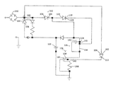
- FIG. 1 is a schematic diagram of a circuit
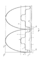
- FIG. 2 is a diagram showing current and voltage over time of the circuit of FIG. 1 .
- FIG. 3 is a diagram showing current and voltage over time of the circuit of FIG. 1 when the circuit is being dimmed.
- Driving circuitry for powering light emitting diode (LED) lights generally rely on digital circuitry to measure the instantaneous value of a driving voltage, on a microprocessor to identify LEDs to activate based on the measured value, and on digital switches to selectively activate the identified LEDs.
- the digital circuitry reduces the overall efficiency of the LED lighting by causing harmonic distortion and power factor distortion in the LED light and the associated power line.
- a current conditioning circuit is presented for selectively routing current to various LED groups in a LED light.
- the current conditioning circuit uses analog components and circuitry for operation, and produces minimal harmonic distortion and power factor distortion.
- the current conditioning circuitry is provided to selectively route current to different LED groups depending on the instantaneous value of an AC input voltage.
- the conditioning circuitry includes only analog circuit components and does not include digital components or digital switches for operation.
- the circuitry relies on depletion-mode metal-oxide-semiconductor field-effect transistor (MOSFET) transistors for operation.
- the depletion MOSFET transistors have a high resistance between their drain and source terminals, and switch between conducting and non-conducting states relatively slowly.
- the depletion-mode MOSFET transistors may conduct current between their drain and source terminals when a voltage V GS between the gate and source terminals is zero or positive and the MOSFET transistor is operating in the saturation (or active, or conducting) mode (or region, or state).
- the current through the depletion-mode MOSFET transistor may be restricted if a negative V GS voltage is applied to the terminals and the MOSFET transistor enters the cutoff (or non-conducting) mode (or region, or state).
- the MOSFET transistor transitions between the saturation and cutoff modes by operating in the linear or ohmic mode or region, in which the amount of current flowing through the transistor (between the drain and source terminals) is dependent on the voltage between the gate and source terminals V GS .
- the depletion MOSFET transistors preferably have an elevated resistance between drain and source (when operating in the linear mode) such that the transistors switch between the saturation and cutoff modes relatively slowly.
- the depletion MOSFET transistors switch between the saturation and cutoff modes by operating in the linear or ohmic region, thereby providing a smooth and gradual transition between the saturation, and cutoff modes.
- a depletion-mode MOSFET transistor may have a threshold voltage of ⁇ 2.6 volts, such that the depletion-mode MOSFET transistor allows substantially no current to pass between the drain and source terminals when the gate-source voltage V GS is below ⁇ 2.6 volts.
- Other values of threshold voltages may alternatively be used.
- FIG. 1 is a schematic diagram showing a conditioning circuit 100 for driving three LED groups using a rectified AC input voltage.
- the conditioning circuit 100 uses analog circuitry to selectively route current to the LED, groups based on the instantaneous value of the AC input voltage.
- the conditioning circuit 100 receives an AC input voltage from an AC voltage source (not shown), such as a power supply, an AC line voltage, or the like.
- the AC voltage source is coupled to a fuse and rectifier (not shown) to provide a rectified AC input as is known in the art.
- the conditioning circuit 100 has a first series interconnection of a first LED group 102 with an anode 104 and cathode 106 .
- the anode 104 is in parallel connection to ancillary circuitry 107 .
- the anode 104 of the first LED group 102 is in parallel connection to an anode 108 of a valley fill LED group 110 of the ancillary circuitry 107 .
- the ancillary circuitry 107 also includes circuit protection elements 109 that in one embodiment is a combination diode and resistor.
- the valley fill LED group 110 additionally has a cathode 112 in series to a resistor 114 .
- the valley fill LED group 110 can consist of one or more LEDs connected in series.
- a capacitor 116 is in connection with the resistor 114 to discharge current to ensure the flow of current through the valley fill LED group 110 throughout a current cycle.
- a second series interconnection of a second LED group 120 with an anode 122 and a cathode 124 is in series with the first series interconnection of the first LED group 102 .
- Each LED group 102 and 120 can be formed of one or more LEDs, or of one or more high-voltage LEDs. In examples in which a LED group includes two or more LEDs (or two or more high-voltage LEDs), the LEDs may be coupled in series and/or in parallel.
- a first depletion MOSFET transistor 126 has a drain 128 , source 130 and gate 132 and is in series connection to the first LED group 102 and parallel connection with the second LED group 120 .
- the drain 128 of the first depletion MOSFET transistor 126 is electrically connected to the cathode 106 of the first LED group 102 while the source 130 is connected in series, to a first sense resistor 134 .
- the cathode 124 of the second LED group 120 is in series connection with the, first sense resistor 134 .
- the gate 132 of the first depletion MOSFET transistor 126 and the sense resistor 134 are connected in series to a second depletion MOSFET transistor 136 having a drain 138 , source 140 and gate 142 . Similar to the first depletion MOSFET transistor 126 , the second depletion MOSFET transistor 136 has its source 140 electrically connected to a second sense resistor 144 . In addition, the cathode of the valley fill LED group 110 is electrically connected in series with the second sense resistor 144 that is connected to a ground.
- the capacitor 116 discharges keeping the voltage at the valley fill LED group 110 above the threshold voltage of the valley fill LED group 110 .
- the valley fill LED group 110 continues to emit light even after the first and second LED groups stop emitting light.
- FIGS. 2-3 are input voltage and circuit current timing diagrams showing the rectified input voltage V rect during one cycle.
- the rectified voltage V rect may be applied at the output of a voltage rectifier 150 to the LED groups 102 and 120 , as shown in driving circuitry 100 of FIG. 1 .
- the exemplary cycle of the rectified input voltage V rect shown in FIG. 2 begins at time t 0 with the rectified input voltage V rect having a value of 0V (0 volts).
- the rectified voltage V rect undergoes a half-sine cycle between times t 0 back to t 0 .
- the value of the rectified input voltage V rect remains below the forward voltage of the first LED group 102 , and no current flows through the first LED group 102 .
- the capacitor 116 discharges, causing current I VP to flow to the valley fill LED group 110 such that the voltage at the valley fill LED group 110 is above a threshold voltage V VP of the valley fill LED group 110 resulting in the valley fill LED group emitting light.
- the forward voltage of the first LED group 102 is reached and current gradually begins to flow through the first LED group 102 .
- the first depletion MOSFET transistor 126 is in a conducting state such that the current flowing from the rectifier through the first LED group 102 flows through the depletion MOSFET transistor 126 (from drain to source terminals) and the first sense resistor 134 .
- the rectified voltage V rect increases in value from V 1 to V 2
- the value of the current flowing through the first LED group 102 , the first depletion MOSFET transistor 126 , and the first sense resistor 134 increases.
- the increase in current through the first sense resistor 134 causes the voltage across the first sense resistor 134 to increase, and the corresponding reverse voltage between the gate and source terminals of the first depletion MOSFET transistor 126 to increase.
- the first depletion MOSFET transistor 126 begins to transition out of saturation and into the “linear” or “ohmic” mode or region of operation.
- the first depletion MOSFET transistor 126 may thus begin to shut down and to conduct less current as the value of the rectified voltage V rect reaches the value V 2 .
- the rectified voltage V rect reaches the value V 2 (at time t 2 )
- the rectified voltage V rect is reaching or exceeding the sum of the forward voltage of the first and second LED groups 102 and 120 .
- the second LED group 120 begins to conduct current
- the current flowing through the first LED group 102 begins to flow through the series interconnection of the second LED group 120 , the second depletion MOSFET transistor 136 , and the Second and first sense resistors 144 and 134 .
- V rect exceeds V 2 and the first depletion MOSFET transistor 126 enters the cutoff mode, most or all of the current flowing through the first LED group 102 flows through the second LED group 120 .
- the rectified voltage V rect decreases from a maximum of V max back to 0 volts.
- the second and first LED groups 102 and 120 are sequentially turned off and gradually stop conducting current.
- V rect remains above V 2
- both the first and second LED groups 102 and 120 remain in the conducting state.
- V rect no longer reaches or exceeds the sum of the forward voltage of the first and second LED groups 102 and 120
- the second LED group 120 begins to turn off and to stop conducting current.
- the voltage drop across the first resistor drops below the threshold voltage of the first depletion MOSFET transistor 126 , and the first depletion MOSFET transistor 126 enters the linear or ohmic operation mode and begins to conduct current once again.
- current flows through the first LED group 102 , the first depletion MOSFET transistor 126 , and the first resistor 134 , and the first LED group 102 thus continues to emit light.
- V rect As the value of V rect reaches or dips below V 1 (at time t 4 ), however, V rect no longer reaches or exceeds the forward voltage of the first LED group 102 , and the first LED group 102 begins to turn off and stop conducting current. As a result, both the first and second LED groups 102 and 120 turn off and stop emitting light during the period [t 4 , t 5 ].
- the capacitor 116 discharges causing current to continue to flow to the valley fill LED group 110 above a threshold voltage of the valley fill LED group 110 even as the input voltage to the circuit approaches and reaches zero cross at t 0 . Therefore, during the period when no input voltage exists and where the input voltage does not reach the threshold voltage of the first LED group 102 light is emitted by the valley fill LED group 110 .
- FIGS. 2-3 also show a current timing diagram showing the current I as a result of current flowing through the first, second and valley fill LED groups 102 , 120 and 110 during one cycle of the rectified voltage V rect .
- a current I VP as a result of the discharging of the capacitor 116 flows through the valley fill LED group 110 even when no voltage is provided by the AC input at t 0 and during the period t 0 -t 1 when the threshold voltage of the first LED group 102 has not been reached.
- the current I through the first LED group 102 begins flowing around time t 1 once the threshold voltage of the first LED group 102 is reached, and increases to a first value I 1 .
- the current I continues to flow through the first LED group 102 from around time t 1 to around time t 4 .
- the current I flows through the second LED group 120 , and reaches a second value I 2 .
- the current I increases to the value I 2 .
- current no longer flows through the first or second LED groups 102 or 120 , current continues to flow through the valley fill LED group 110 . This current continues to flow from the time t 5 of a first cycle to the time t 1 of a next cycle.
- the t 5 or t 1 period of time is typically a period when no current is flowing in the circuit and no light is being emitted by the LED groups.
- the shape of the current on the represented current timing diagram is referred to as a valley.
- the LED group 110 is referred to as the valley fill LED group 110 because the valley fill circuit allows current to flow in the circuit during this t 5 to t 1 time period filling the valley created on the current timing diagram with a low level of current flow. This results in light being emitted during this period by the valley fill LED group 110 , thus providing a constant lighting output through the cycle.
- the forward voltages of the first and second LED groups 102 and 120 and valley fill LED group 110 may determine the value of the voltages V 1 , V 2 and V VP at which the LED groups are activated.
- the voltage V 1 may be substantially equal to the forward voltage of the first LED group
- the voltage V 2 may be substantially equal to the sum of the forward voltages of the first and second LED groups just as the forward voltage of the valley fill LED group
- V VP may be substantially equal to the sum of the forward voltages of the valley fill LED group 110 .
- the forward voltage of the first LED group 102 may be set to a value of 60V, for example, while the forward voltage of the second LED group may be set to a value of 40V, such that the voltage V 1 is approximately equal to 60V and the voltage V 2 is approximately equal to 100V.
- the value of the first resistor 134 may be set such that the first depletion MOSFET transistor 126 enters a non-conducting state when the voltage V rect reaches a value of V 2 .
- the value of the first resistor 134 may be set based on the threshold voltage of the first depletion MOSFET transistor 126 , the drain-source resistance of the first depletion MOSFET transistor 126 , and the voltages V 1 and V 2 .
- the first resistor may have a value of around 31.6 ohms.
- the conditioning circuitry 100 of FIG. 1 can be used to provide dimmable lighting using the first and second LED groups 102 and 120 .
- the conditioning circuitry can, in particular, provide a variable lighting intensity based on the amplitude of the rectified driving voltage V rect .
- FIG. 1D is a voltage timing diagram showing the effects of a reduced driving voltage amplitude on the LED lighting circuitry 100 .
- a portion of the driving voltage V rect has been cut.
- the driving voltage V rect may have been cut or reduced through the activation of a potentiometer, a dimmer switch, or other appropriate means. While the driving voltage is cut, the threshold voltages V 1 and V 2 remain constant as the threshold voltages are set by parameters of the components of the circuit 100 .
- the driving voltage V rect is cut, the driving voltage takes a time [t 0 , t 1 ′] to reach the first threshold voltage V 1 during the first half of each cycle that is longer than the time [t 0 , t 1 ]. Similarly, the driving voltage may fail to reach the second threshold voltage. As a result, the time-period [t 1 ′, t 4 ′] during which current flows through the first LED group 102 is substantially reduced with respect to the corresponding time-period [t 1 ] when the input voltage is not cut.
- each of the first and second LED groups 102 and 120 is dependent on the total amount of current flowing through the LED groups, the shortening of the time-periods during which current flows through each of the LED groups causes the lighting intensity produced by each of the LED groups to be reduced.
- the capacitor 116 discharges to provide current that flows through the valley fill LED group 110 such that light is emitted by the valley fill LED group 110 as long as current continues to flew through the circuit 100 via an electrical input.
- a phase cut dimmer as is represented in FIG. 3
- current I VP continues to flow through the valley fill LED group 110 . Therefore, during this period of the cycle constant light is emitted by the circuit 100 as long as input current is provided to the circuit 100 .
- the conditioning circuitry 100 of FIG. 1 can be used to provide color-dependent dimmable lighting.
- the first and second LED groups may include LEDs of different colors, or different combinations of LEDs having different colors.
- V rect When a full amplitude voltage V rect is provided, the light output of the conditioning circuitry 100 is provided by both the first and second LED groups, and the color of the light output is determined based on the relative light intensity and the respective color light provided by each of the LED groups.
- the light intensity provided by the second LED group will be reduced more rapidly than the light intensity provided by the first LED group.
- the light output of the conditioning circuitry 100 will gradually be dominated by the light output (and the color of light) produced by the first LED group.
- the color of the valley fill LED group 110 shall be constant throughout the cycle.
- a color or a predetermined range of wavelengths is chosen to cause a biological reaction in a plant or animal that is being illuminated by the light source.
- the valley fill LED group 110 emits a narrow range of wavelengths in the green band of wavelengths (between 495 nm and 570 nm).
- the valley fill LED group 110 emits a narrow range of wavelengths in the UV range (below 400 nm).
- Other narrow ranges can be selected by a user depending on the biological needs of the living organisms that receive the light.
- the circuit 100 may have three voltage thresholds V 1 , V 2 , and V VP at which different LED groups are activated.
- the first LED group 102 has a driving voltage V rect that exceeds the first voltage threshold V 1
- the second LED group 120 may be activated for a period [t 2 , t 3 ] ( FIG. 2 ) during which the driving voltage V rect exceeds the second voltage threshold V 2
- the valley fill LED group 110 may is activated even during a period [t 5 , t 1 ] during which the driving voltage V rect exceeds the voltage threshold V VP of the valley fill LED group 110 but does not exceed the voltage threshold V 1 or V 2 of the first and second LED groups 102 and 120 .
- As voltage decreases during the period [t 4 -t 5 ] the driving voltage drops below the threshold voltage of the second LED group 120 .
- the capacitor 116 ensures the threshold voltage of the valley fill LED group 110 is exceeded within the circuit, even at a time the input voltage approaches and is at zero cross t 0 . Then this cycle repeats, with the threshold voltage of the valley fill LED group 110 continuously exceeded from t 0 to t 0 as long as an input electrical signal is being supplied to the circuit 100 .
- circuit 100 is a two-stage circuit having a first LED group 102 , first depletion MOSFET transistor 126 and first sense resistor 134 in a first stage and a second LED group 120 , second depletion MOSFET transistor 136 and second sense resistor 144 in a second stage
- additional stages can be added to the circuit with additional LED groups, depletion MOSFET transistors and sense resistors as is known in the art. With each additional stage added additional threshold voltages are provided that when exceeded allow current to flow through the additional LED groups identically to the first and second LED groups 102 and 120 as described.
- circuit 100 is described as utilizing depletion MOSFET transistors, other transistors and combinations of transistors can be utilized that provide the same functionality as the MOSFET transistors by holding current constant until threshold voltages of LED groups are met as is known in the art.
- ancillary circuitry 107 can be implemented in all such circuits to provide the valley fill functionality described without falling outside the scope of this disclosure.
- the valley fill LED group 110 By having ancillary circuitry 107 with the capacitor 116 provides a charge for the diodes in the valley fill LED group 110 to ensure current is always flowing to the valley fill LED group 110 to provide a low level of light output at all times. Even when dimmed through phase cutting, the valley fill LED group 110 continues to receive current and operate to provide light during operation of the circuit 100 . At no time during operation does current cease to flow through the valley fill LED group 110 ensuring no Periods of the absence of light exist during operation preventing the detection of such periods and reducing gap between the peak of the sine wave to the valley of the sine wave. Thus flicker and dimming properties are improved.
- valley fill LED group 110 can have a predetermined color such as green or UV known to enhance the growth of animals or plants while the other LED groups 102 and 120 can have their own predetermined color again to enhance the growth of plants, animals, aquatic life or the like.
- Each of the first, second and valley fill LED groups 102 , 120 and 110 has a forward voltage (or threshold voltage).
- the forward voltage generally is a minimum voltage required across the LED group in order for current to flow through the LED group, and/or for light to be emitted by the LED group.
- the first, second and valley fill LED groups 102 , 120 and 110 may have the same forward voltage (e.g., 50 volts), or the first, second and valley fill LED groups 102 , 120 and 110 may have different forward voltages (e.g., 60 volts, 50 volts, and 40 volts, respectively). Therefore the gap between peak current and the current at a valley, or minimum current, is reduced to improve dimming properties and provide additional functionality to a lighting device. This is accomplished without utilizing an ancillary transistor, thus reducing cost and minimizing complexities.
- the conditioning circuit shown and described in this application, and shown in the figures, and the various modifications to conditioning circuits described in the application, are configured to drive LED lighting circuits with reduced or minimal total harmonic distortion.
- the conditioning circuits provide a high lighting efficiency by driving one, two, or more LED groups based on the instantaneous value of the driving voltage.
- the depletion MOSFET transistors transition between the saturation and cutoff modes relatively slowly.
- the transistors gradually switch between conducting and non-conducting states, the switching on and off of the LED groups and transistors follows substantially sinusoidal contours.
- the circuitry produces little harmonic distortion as the LED groups are gradually activated and deactivated.
- the first and second (or more) LED groups control current through each other: the forward voltage level of the second LED group influences the current flow through the first LED group, and the forward voltage level of the first LED group influences the current flow through the second LED group.
- the circuitry is self-controlling through the interactions between the multiple LED groups and multiple MOSFET transistors.
- field effect transistor may refer to any of a variety of multi-terminal transistors generally operating on the principals of controlling an electric field to control the shape and hence the conductivity of a channel of one type of charge carrier in a semiconductor material, including, but not limited to a metal oxide semiconductor field effect transistor (MOSFET), a junction FET (JFET), a metal semiconductor FET (MESFET), a high electron mobility transistor (HEMT), a modulation doped FET (MODFET), an insulated gate bipolar transistor (IGBT), a fast reverse epitaxial diode FET (FREDFET), and an ion-sensitive FET (ISFET).
- MOSFET metal oxide semiconductor field effect transistor
- JFET junction FET
- MESFET metal semiconductor FET
- HEMT high electron mobility transistor
- MODFET modulation doped FET
- IGBT fast reverse epitaxial diode FET
- ISFET ion-sensitive FET
- the terms “base,” “emitter,” and “collector” may refer to three terminals of a transistor and may refer to a base, an emitter and a collector of a bipolar junction transistor or may refer to a gate, a source, and a drain of a field effect transistor, respectively, and vice versa.
- the terms “gate,” “source,” and “drain” may refer to “tease,” “emitter,” and “collector” of a transistor, respectively, and vice versa.
- various configurations described in the present disclosure may be implemented on a Silicon, Silicon-Germanium (SiGe), Gallium Arsenide (GaAs), Indium Phosphide (InP) or Indium Gallium Phosphide (InGaP) substrate, or any other suitable substrate.
- SiGe Silicon, Silicon-Germanium
- GaAs Gallium Arsenide
- Indium Phosphide InP
- InGaP Indium Gallium Phosphide
- a resistor May refer to one or more resistors
- a voltage may refer to one or more voltages
- a current may refer to one or more currents
- a signal may refer to differential voltage signals.
- a phrase such as an “example” or an “aspect” does not imply that such example or aspect is essential to the subject technology or that such aspect applies to all configurations of the subject technology.
- a disclosure relating to an example or an aspect may apply to all configurations, or one or more configurations.
- An aspect may provide one or more examples.
- a phrase such as an aspect may refer to one or more aspects and vice versa.
- a phrase such as an “embodiment” does not imply that such embodiment is essential to the subject technology or that such embodiment applies to all configurations of the subject technology.
- a disclosure relating to an embodiment may apply to all embodiments, or one or more embodiments.
- An embodiment may provide one or more examples.
- a phrase such as an embodiment may refer to one or more embodiments and vice versa.
- a phrase such as a “configuration” does not imply that such configuration is essential to the subject technology or that such configuration applies to all configurations of the subject technology.
- a disclosure relating to a configuration may apply to all configurations, or one or more configurations.
- a configuration may provide one or more examples.
- a phrase such a configuration may refer to one or more configurations and vice versa.
- actions or functions when actions or functions are described as being performed by an item (e.g., routing, lighting, emitting, driving, flowing, generating, activating, turning on or off, selecting, controlling, transmitting, sending, or any other action or function), it is understood that such actions or functions may be performed by the item directly or indirectly.
- the module when a module is described as performing an action, the module may be understood to perform the action directly.
- the module when a module is described as performing an action, the module may be understood to perform the action indirectly, for example, by facilitating, enabling or causing such an action.
- the term “coupled”, “connected”, “interconnected”, or the like may refer to being directly coupled, connected, or interconnected (e.g., directly electrically coupled, connected, or interconnected). In another aspect, the term “coupled”, “connected”, “interconnected”, or the like may refer to being indirectly coupled, connected, or interconnected (e.g., indirectly electrically coupled, connected, or interconnected).
Landscapes
- Circuit Arrangement For Electric Light Sources In General (AREA)
Abstract
Description
- This application is based upon and claims benefit to U.S. Provisional Patent Application Ser. No. 62/402,631 filed Sep. 30, 2017 entitled Dimmable Analog AC Circuit to Grajcar, et al. and that application is incorporated by reference in full.
- This invention relates to LED lighting circuits. More specifically this invention relates to a circuit for providing improved operation of an LED lighting device.
- LED lighting as an energy efficient lighting source is becoming more and more popular world-wide. Several ways exist regarding how to successfully operate and dim LED devices. In particular, typically line voltage is AC or alternating current voltage where the voltage and current are represented by a sine wave. One circuit that can be used to operate and dim LED utilizes a rectifier and AC to DC converter in association with a PWM device to provide diming.
- In an alternative embodiment applicant eliminated the AC to DC converter and need for a PWM device through conditioning the AC current directly provided to the LEDs. This is shown in applicant's U.S. Pat. No. 8,373,363 that is incorporated in full herein. While effective at operating and dimming, problems remain. During analog operation there are times during operation where current exists at zero cross for extended periods of time. For certain operations light is desired during this period. As one example, some flicker indexes put out by specification makers focus, not just on frequency of the AC sine wave, but also on the drop in current from peak to the valley of the sine wave. In another embodiment, in agricultural and horticulture applications applicant has found that low levels of green light can be beneficial to animal and plant growth and should be used in combination with other colored lighting to optimize growth in animals and plants. Thus a need exists in analog circuits to reduce the gap between peak current and the current at a valley to improve dimming properties and provide additional functionality to a lighting device.
- Therefore, a principle object of the present invention is to improve dimming functionality of an AC analog circuit.
- Yet another object of the present invention, is to improve functionality on an AC analog circuit.
- These and other object, feature and advantages will become apparent from the specification and claims
- A circuit having a first series interconnection of a first light-emitting diode (LED) group, a first transistor, a first resistor, a second series interconnection of a second LED group, a second transistor, and a second resistor. The first series interconnection has a cathode coupled to a drain terminal of the first transistor and a source terminal of the first transistor is coupled to a first terminal of the first resistor wherein voltage across the first resistor provides a biasing voltage for the first transistor. The second series interconnection is coupled to a drain terminal of the second transistor and a first terminal of the second resistor wherein voltage across the second resistor provides a biasing voltage for the second transistor. The circuit additionally has ancillary circuitry bypassing the first series interconnection and having a capacitor to continuously provide current to the first series interconnection such that the first series interconnection continuously emits light during operation of the circuit and the capacitor is connected between the drain of the second transistor and a rectifier. By providing the continuous current functioning is improved.
-
FIG. 1 is a schematic diagram of a circuit; -
FIG. 2 is a diagram showing current and voltage over time of the circuit ofFIG. 1 . -
FIG. 3 is a diagram showing current and voltage over time of the circuit ofFIG. 1 when the circuit is being dimmed. - In the following detailed description, numerous specific details are set forth by way of examples in order to provide a thorough understanding of the relevant teachings. However, it should be apparent to those skilled in the art that the present teachings may be practiced without such details. In other instances, well known methods, procedures, components, and/or circuitry have been described at a relatively high-level, without detail, in order to avoid unnecessarily obscuring aspects of the present teachings.
- Driving circuitry for powering light emitting diode (LED) lights generally rely on digital circuitry to measure the instantaneous value of a driving voltage, on a microprocessor to identify LEDs to activate based on the measured value, and on digital switches to selectively activate the identified LEDs. The digital circuitry, however, reduces the overall efficiency of the LED lighting by causing harmonic distortion and power factor distortion in the LED light and the associated power line. In order to reduce the harmonic distortion and power factor distortion caused by the digital circuitry, a current conditioning circuit is presented for selectively routing current to various LED groups in a LED light. The current conditioning circuit uses analog components and circuitry for operation, and produces minimal harmonic distortion and power factor distortion.
- The current conditioning circuitry is provided to selectively route current to different LED groups depending on the instantaneous value of an AC input voltage. In a preferred embodiment, the conditioning circuitry includes only analog circuit components and does not include digital components or digital switches for operation.
- The circuitry relies on depletion-mode metal-oxide-semiconductor field-effect transistor (MOSFET) transistors for operation. In a preferred embodiment, the depletion MOSFET transistors have a high resistance between their drain and source terminals, and switch between conducting and non-conducting states relatively slowly. The depletion-mode MOSFET transistors may conduct current between their drain and source terminals when a voltage VGS between the gate and source terminals is zero or positive and the MOSFET transistor is operating in the saturation (or active, or conducting) mode (or region, or state). The current through the depletion-mode MOSFET transistor, however, may be restricted if a negative VGS voltage is applied to the terminals and the MOSFET transistor enters the cutoff (or non-conducting) mode (or region, or state).
- The MOSFET transistor transitions between the saturation and cutoff modes by operating in the linear or ohmic mode or region, in which the amount of current flowing through the transistor (between the drain and source terminals) is dependent on the voltage between the gate and source terminals VGS. In one example, the depletion MOSFET transistors preferably have an elevated resistance between drain and source (when operating in the linear mode) such that the transistors switch between the saturation and cutoff modes relatively slowly. The depletion MOSFET transistors switch between the saturation and cutoff modes by operating in the linear or ohmic region, thereby providing a smooth and gradual transition between the saturation, and cutoff modes. In one example, a depletion-mode MOSFET transistor may have a threshold voltage of −2.6 volts, such that the depletion-mode MOSFET transistor allows substantially no current to pass between the drain and source terminals when the gate-source voltage VGS is below −2.6 volts. Other values of threshold voltages may alternatively be used.
-
FIG. 1 is a schematic diagram showing aconditioning circuit 100 for driving three LED groups using a rectified AC input voltage. Theconditioning circuit 100 uses analog circuitry to selectively route current to the LED, groups based on the instantaneous value of the AC input voltage. Theconditioning circuit 100 receives an AC input voltage from an AC voltage source (not shown), such as a power supply, an AC line voltage, or the like. The AC voltage source is coupled to a fuse and rectifier (not shown) to provide a rectified AC input as is known in the art. - The
conditioning circuit 100 has a first series interconnection of afirst LED group 102 with ananode 104 andcathode 106. Theanode 104 is in parallel connection to ancillary circuitry 107. In particular theanode 104 of thefirst LED group 102 is in parallel connection to ananode 108 of a valley fill LED group 110 of the ancillary circuitry 107. The ancillary circuitry 107 also includescircuit protection elements 109 that in one embodiment is a combination diode and resistor. The valley fill LED group 110 additionally has acathode 112 in series to a resistor 114. The valley fill LED group 110 can consist of one or more LEDs connected in series. Acapacitor 116 is in connection with the resistor 114 to discharge current to ensure the flow of current through the valley fill LED group 110 throughout a current cycle. - A second series interconnection of a
second LED group 120 with ananode 122 and acathode 124 is in series with the first series interconnection of thefirst LED group 102. EachLED group - In a bypass path, a first
depletion MOSFET transistor 126 has adrain 128,source 130 andgate 132 and is in series connection to thefirst LED group 102 and parallel connection with thesecond LED group 120. Thedrain 128 of the firstdepletion MOSFET transistor 126 is electrically connected to thecathode 106 of thefirst LED group 102 while thesource 130 is connected in series, to afirst sense resistor 134. In addition, thecathode 124 of thesecond LED group 120 is in series connection with the,first sense resistor 134. Thegate 132 of the firstdepletion MOSFET transistor 126 and thesense resistor 134 are connected in series to a seconddepletion MOSFET transistor 136 having adrain 138,source 140 andgate 142. Similar to the firstdepletion MOSFET transistor 126, the seconddepletion MOSFET transistor 136 has itssource 140 electrically connected to asecond sense resistor 144. In addition, the cathode of the valley fill LED group 110 is electrically connected in series with thesecond sense resistor 144 that is connected to a ground. - In operation, current flows to the
first LED group 102 and the valley fill LED group 110. Upon reaching a threshold voltage of the valley fill LED group 110 current flows through the valley fill LED group 110 emitting light at a low level. Simultaneously, as the voltage increases it reaches the threshold voltage of thefirst LED group 102 and current begins flowing through thefirst LED group 102. Specifically the threshold voltage of the valley fill LED group 110 is less than the threshold voltage of thefirst LED group 102. - As current flows through the
first LED group 102, prior to reaching a threshold voltage of thesecond LED group 120 current is dynamically bypassed from the second LED group to the firstdepletion MOSFET transistor 126 until the threshold voltage of thesecond LED group 120 is reached. At that point the current flows through thesecond LED group 120. As the voltage cycle continues and voltage falls below the threshold value of thesecond LED group 120, current stops flowing through thesecond LED group 120 and light is no longer emitted from thesecond LED group 120. Similarly, once the voltage falls below the threshold voltage of thefirst LED group 102 current stops flowing through thefirst LED group 102 and thefirst LED group 102 stops emitting light. - As the input voltage of the AC input falls below the threshold voltage of the valley fill LED group 110, the
capacitor 116 discharges keeping the voltage at the valley fill LED group 110 above the threshold voltage of the valley fill LED group 110. As a result, the valley fill LED group 110 continues to emit light even after the first and second LED groups stop emitting light. - In operation, in the driving
circuitry 100 ofFIG. 1 , one or both of theLED groups LED groups LED driving circuitry 100 ofFIG. 1 will be explained with reference to the input voltage and circuit current timing diagrams ofFIG. 2-3 .FIGS. 2-3 are input voltage and circuit current timing diagrams showing the rectified input voltage Vrect during one cycle. The rectified voltage Vrect may be applied at the output of avoltage rectifier 150 to theLED groups circuitry 100 ofFIG. 1 . - The exemplary cycle of the rectified input voltage Vrect shown in
FIG. 2 begins at time t0 with the rectified input voltage Vrect having a value of 0V (0 volts). The rectified voltage Vrect undergoes a half-sine cycle between times t0 back to t0. Between times t0 and t1, the value of the rectified input voltage Vrect remains below the forward voltage of thefirst LED group 102, and no current flows through thefirst LED group 102. During this time period, t0 and t1, during a sinusoidal cycle, thecapacitor 116 discharges, causing current IVP to flow to the valley fill LED group 110 such that the voltage at the valley fill LED group 110 is above a threshold voltage VVP of the valley fill LED group 110 resulting in the valley fill LED group emitting light. - As the rectified voltage Vrect reaches a value of V1, the forward voltage of the
first LED group 102 is reached and current gradually begins to flow through thefirst LED group 102. At this time, the firstdepletion MOSFET transistor 126 is in a conducting state such that the current flowing from the rectifier through thefirst LED group 102 flows through the depletion MOSFET transistor 126 (from drain to source terminals) and thefirst sense resistor 134. - As the rectified voltage Vrect increases in value from V1 to V2, the value of the current flowing through the
first LED group 102, the firstdepletion MOSFET transistor 126, and thefirst sense resistor 134 increases. The increase in current through thefirst sense resistor 134 causes the voltage across thefirst sense resistor 134 to increase, and the corresponding reverse voltage between the gate and source terminals of the firstdepletion MOSFET transistor 126 to increase. As the reverse gate-source voltage increases, however, the firstdepletion MOSFET transistor 126 begins to transition out of saturation and into the “linear” or “ohmic” mode or region of operation. The firstdepletion MOSFET transistor 126 may thus begin to shut down and to conduct less current as the value of the rectified voltage Vrect reaches the value V2. - Meanwhile, as the rectified voltage. Vrect reaches the value V2 (at time t2), the rectified voltage Vrect is reaching or exceeding the sum of the forward voltage of the first and
second LED groups second LED group 120 begins to conduct current, and the current flowing through thefirst LED group 102 begins to flow through the series interconnection of thesecond LED group 120, the seconddepletion MOSFET transistor 136, and the Second andfirst sense resistors depletion MOSFET transistor 126 enters the cutoff mode, most or all of the current flowing through thefirst LED group 102 flows through thesecond LED group 120. - Thus, during the first half of the cycle, no current initially flows through either of the first and
second LED groups first LED group 102 which starts to emit light (period [t0, t1]) while thesecond LED group 120 remains off. Finally, as the value of Vrect reaches or exceeds V2, current begins to flow through both the first andsecond LED groups - During the second half of the cycle, the rectified voltage Vrect decreases from a maximum of Vmax back to 0 volts. During this period, the second and
first LED groups second LED groups second LED groups second LED group 120 begins to turn off and to stop conducting current. At around the same time, the voltage drop across the first resistor drops below the threshold voltage of the firstdepletion MOSFET transistor 126, and the firstdepletion MOSFET transistor 126 enters the linear or ohmic operation mode and begins to conduct current once again. As a result, current flows through thefirst LED group 102, the firstdepletion MOSFET transistor 126, and thefirst resistor 134, and thefirst LED group 102 thus continues to emit light. - As the value of Vrect reaches or dips below V1 (at time t4), however, Vrect no longer reaches or exceeds the forward voltage of the
first LED group 102, and thefirst LED group 102 begins to turn off and stop conducting current. As a result, both the first andsecond LED groups capacitor 116 discharges causing current to continue to flow to the valley fill LED group 110 above a threshold voltage of the valley fill LED group 110 even as the input voltage to the circuit approaches and reaches zero cross at t0. Therefore, during the period when no input voltage exists and where the input voltage does not reach the threshold voltage of thefirst LED group 102 light is emitted by the valley fill LED group 110. -
FIGS. 2-3 also show a current timing diagram showing the current I as a result of current flowing through the first, second and valleyfill LED groups - As described in relation to
FIG. 2 , a current IVP as a result of the discharging of thecapacitor 116 flows through the valley fill LED group 110 even when no voltage is provided by the AC input at t0 and during the period t0-t1 when the threshold voltage of thefirst LED group 102 has not been reached. The current I through thefirst LED group 102 begins flowing around time t1 once the threshold voltage of thefirst LED group 102 is reached, and increases to a first value I1. The current I continues to flow through thefirst LED group 102 from around time t1 to around time t4. Between times t2 and t3, the current I flows through thesecond LED group 120, and reaches a second value I2. During the time period [t2, t3], the current I increases to the value I2. At the time t5 current no longer flows through the first orsecond LED groups - The t5 or t1 period of time is typically a period when no current is flowing in the circuit and no light is being emitted by the LED groups. As a result, the shape of the current on the represented current timing diagram is referred to as a valley. Hence, the LED group 110 is referred to as the valley fill LED group 110 because the valley fill circuit allows current to flow in the circuit during this t5 to t1 time period filling the valley created on the current timing diagram with a low level of current flow. This results in light being emitted during this period by the valley fill LED group 110, thus providing a constant lighting output through the cycle.
- In general, electrical parameters of the components of driving
circuit 100 can be selected to adjust the functioning of thecircuit 100. For example, the forward voltages of the first andsecond LED groups - In one example, the forward voltage of the
first LED group 102 may be set to a value of 60V, for example, while the forward voltage of the second LED group may be set to a value of 40V, such that the voltage V1 is approximately equal to 60V and the voltage V2 is approximately equal to 100V. In addition, the value of thefirst resistor 134 may be set such that the firstdepletion MOSFET transistor 126 enters a non-conducting state when the voltage Vrect reaches a value of V2. As such the value of thefirst resistor 134 may be set based on the threshold voltage of the firstdepletion MOSFET transistor 126, the drain-source resistance of the firstdepletion MOSFET transistor 126, and the voltages V1 and V2. In one example, the first resistor may have a value of around 31.6 ohms. - The
conditioning circuitry 100 ofFIG. 1 can be used to provide dimmable lighting using the first andsecond LED groups FIG. 1D is a voltage timing diagram showing the effects of a reduced driving voltage amplitude on theLED lighting circuitry 100. - As shown in.
FIG. 3 , a portion of the driving voltage Vrect has been cut. The driving voltage Vrect may have been cut or reduced through the activation of a potentiometer, a dimmer switch, or other appropriate means. While the driving voltage is cut, the threshold voltages V1 and V2 remain constant as the threshold voltages are set by parameters of the components of thecircuit 100. - Because the driving voltage Vrect is cut, the driving voltage takes a time [t0, t1′] to reach the first threshold voltage V1 during the first half of each cycle that is longer than the time [t0, t1]. Similarly, the driving voltage may fail to reach the second threshold voltage. As a result, the time-period [t1′, t4′] during which current flows through the
first LED group 102 is substantially reduced with respect to the corresponding time-period [t1] when the input voltage is not cut. Because the lighting intensity produced by each of the first andsecond LED groups - In addition, one will appreciate that during a process, such as a dimming process in which voltage is reduced the
capacitor 116 discharges to provide current that flows through the valley fill LED group 110 such that light is emitted by the valley fill LED group 110 as long as current continues to flew through thecircuit 100 via an electrical input. Thus, as an example, when a phase cut dimmer as is represented inFIG. 3 is provided a portion of the input voltage is eliminated and current IVP continues to flow through the valley fill LED group 110. Therefore, during this period of the cycle constant light is emitted by thecircuit 100 as long as input current is provided to thecircuit 100. - In addition to providing dimmable lighting, the
conditioning circuitry 100 ofFIG. 1 can be used to provide color-dependent dimmable lighting. In order to provide color-dependent dimmable lighting, the first and second LED groups may include LEDs of different colors, or different combinations of LEDs having different colors. When a full amplitude voltage Vrect is provided, the light output of theconditioning circuitry 100 is provided by both the first and second LED groups, and the color of the light output is determined based on the relative light intensity and the respective color light provided by each of the LED groups. - As the amplitude of the voltage Vrect is reduced, however, the light intensity provided by the second LED group will be reduced more rapidly than the light intensity provided by the first LED group. As a result, the light output of the
conditioning circuitry 100 will gradually be dominated by the light output (and the color of light) produced by the first LED group. - Additionally, the color of the valley fill LED group 110 shall be constant throughout the cycle. Thus depending upon the application, a color or a predetermined range of wavelengths is chosen to cause a biological reaction in a plant or animal that is being illuminated by the light source. In one embodiment the valley fill LED group 110 emits a narrow range of wavelengths in the green band of wavelengths (between 495 nm and 570 nm). In another embodiment the valley fill LED group 110 emits a narrow range of wavelengths in the UV range (below 400 nm). Other narrow ranges can be selected by a user depending on the biological needs of the living organisms that receive the light.
- The
circuit 100 may have three voltage thresholds V1, V2, and VVP at which different LED groups are activated. In particular, thefirst LED group 102 has a driving voltage Vrect that exceeds the first voltage threshold V1, thesecond LED group 120 may be activated for a period [t2, t3] (FIG. 2 ) during which the driving voltage Vrect exceeds the second voltage threshold V2, and the valley fill LED group 110 may is activated even during a period [t5, t1] during which the driving voltage Vrect exceeds the voltage threshold VVP of the valley fill LED group 110 but does not exceed the voltage threshold V1 or V2 of the first andsecond LED groups second LED group 120. - As input voltage continues to decrease and drops below the threshold voltage of the valley fill LED group 110, the
capacitor 116 ensures the threshold voltage of the valley fill LED group 110 is exceeded within the circuit, even at a time the input voltage approaches and is at zero cross t0. Then this cycle repeats, with the threshold voltage of the valley fill LED group 110 continuously exceeded from t0 to t0 as long as an input electrical signal is being supplied to thecircuit 100. - While the
circuit 100 provided, is a two-stage circuit having afirst LED group 102, firstdepletion MOSFET transistor 126 andfirst sense resistor 134 in a first stage and asecond LED group 120, seconddepletion MOSFET transistor 136 andsecond sense resistor 144 in a second stage, additional stages can be added to the circuit with additional LED groups, depletion MOSFET transistors and sense resistors as is known in the art. With each additional stage added additional threshold voltages are provided that when exceeded allow current to flow through the additional LED groups identically to the first andsecond LED groups - Additionally, while the
circuit 100 is described as utilizing depletion MOSFET transistors, other transistors and combinations of transistors can be utilized that provide the same functionality as the MOSFET transistors by holding current constant until threshold voltages of LED groups are met as is known in the art. One will appreciate the ancillary circuitry 107 can be implemented in all such circuits to provide the valley fill functionality described without falling outside the scope of this disclosure. - By having ancillary circuitry 107 with the
capacitor 116 provides a charge for the diodes in the valley fill LED group 110 to ensure current is always flowing to the valley fill LED group 110 to provide a low level of light output at all times. Even when dimmed through phase cutting, the valley fill LED group 110 continues to receive current and operate to provide light during operation of thecircuit 100. At no time during operation does current cease to flow through the valley fill LED group 110 ensuring no Periods of the absence of light exist during operation preventing the detection of such periods and reducing gap between the peak of the sine wave to the valley of the sine wave. Thus flicker and dimming properties are improved. This also allows for increased functionality because the valley fill LED group 110 can have a predetermined color such as green or UV known to enhance the growth of animals or plants while theother LED groups - Each of the first, second and valley
fill LED groups fill LED groups fill LED groups - The conditioning circuit shown and described in this application, and shown in the figures, and the various modifications to conditioning circuits described in the application, are configured to drive LED lighting circuits with reduced or minimal total harmonic distortion. By using analog circuitry which gradually and selectively routes current to various LED groups, the conditioning circuits provide a high lighting efficiency by driving one, two, or more LED groups based on the instantaneous value of the driving voltage.
- Furthermore, by using depletion MOSFET transistors with elevated drain-source resistances rde, the depletion MOSFET transistors transition between the saturation and cutoff modes relatively slowly. As such, by ensuring that, the transistors gradually switch between conducting and non-conducting states, the switching on and off of the LED groups and transistors follows substantially sinusoidal contours. As a result, the circuitry produces little harmonic distortion as the LED groups are gradually activated and deactivated.
- In addition, the first and second (or more) LED groups control current through each other: the forward voltage level of the second LED group influences the current flow through the first LED group, and the forward voltage level of the first LED group influences the current flow through the second LED group. As a result, the circuitry is self-controlling through the interactions between the multiple LED groups and multiple MOSFET transistors.
- In one aspect, the term “field effect transistor (FET)” may refer to any of a variety of multi-terminal transistors generally operating on the principals of controlling an electric field to control the shape and hence the conductivity of a channel of one type of charge carrier in a semiconductor material, including, but not limited to a metal oxide semiconductor field effect transistor (MOSFET), a junction FET (JFET), a metal semiconductor FET (MESFET), a high electron mobility transistor (HEMT), a modulation doped FET (MODFET), an insulated gate bipolar transistor (IGBT), a fast reverse epitaxial diode FET (FREDFET), and an ion-sensitive FET (ISFET).
- In one aspect, the terms “base,” “emitter,” and “collector” may refer to three terminals of a transistor and may refer to a base, an emitter and a collector of a bipolar junction transistor or may refer to a gate, a source, and a drain of a field effect transistor, respectively, and vice versa. In another aspect, the terms “gate,” “source,” and “drain” may refer to “tease,” “emitter,” and “collector” of a transistor, respectively, and vice versa.
- Unless otherwise mentioned, various configurations described in the present disclosure may be implemented on a Silicon, Silicon-Germanium (SiGe), Gallium Arsenide (GaAs), Indium Phosphide (InP) or Indium Gallium Phosphide (InGaP) substrate, or any other suitable substrate.
- A reference to an element in the singular is not intended to mean “one and only one” unless specifically so stated, but rather “one or more.” For example, a resistor May refer to one or more resistors, a voltage may refer to one or more voltages, a current may refer to one or more currents, and a signal may refer to differential voltage signals.
- The word “exemplary” is used herein to mean “serving as an example or illustration.” Any aspect or design described herein as “exemplary” is not necessarily to be construed as preferred or advantageous over other aspects or designs. In one aspect, various alternative configurations and operations described herein may be considered to be at least equivalent.
- A phrase such as an “example” or an “aspect” does not imply that such example or aspect is essential to the subject technology or that such aspect applies to all configurations of the subject technology. A disclosure relating to an example or an aspect may apply to all configurations, or one or more configurations. An aspect may provide one or more examples. A phrase such as an aspect may refer to one or more aspects and vice versa.
- A phrase such as an “embodiment” does not imply that such embodiment is essential to the subject technology or that such embodiment applies to all configurations of the subject technology. A disclosure relating to an embodiment may apply to all embodiments, or one or more embodiments. An embodiment may provide one or more examples. A phrase such as an embodiment may refer to one or more embodiments and vice versa. A phrase such as a “configuration” does not imply that such configuration is essential to the subject technology or that such configuration applies to all configurations of the subject technology.
- A disclosure relating to a configuration may apply to all configurations, or one or more configurations. A configuration may provide one or more examples. A phrase such a configuration may refer to one or more configurations and vice versa.
- In one aspect of the disclosure, when actions or functions are described as being performed by an item (e.g., routing, lighting, emitting, driving, flowing, generating, activating, turning on or off, selecting, controlling, transmitting, sending, or any other action or function), it is understood that such actions or functions may be performed by the item directly or indirectly. In one aspect, when a module is described as performing an action, the module may be understood to perform the action directly. In one aspect, when a module is described as performing an action, the module may be understood to perform the action indirectly, for example, by facilitating, enabling or causing such an action.
- In one aspect, unless otherwise stated, all measurements, values, ratings, positions, magnitudes, sizes, and other specifications that are set forth in this specification, including in the claims that follow, are approximate, not exact. In one aspect, they are intended to have a reasonable range that is consistent with the functions to which they relate and with what is customary in the art to which they pertain. In one aspect, the term “coupled”, “connected”, “interconnected”, or the like may refer to being directly coupled, connected, or interconnected (e.g., directly electrically coupled, connected, or interconnected). In another aspect, the term “coupled”, “connected”, “interconnected”, or the like may refer to being indirectly coupled, connected, or interconnected (e.g., indirectly electrically coupled, connected, or interconnected).
- The disclosure is provided to enable any person skilled in the art to practice, the various aspects described herein. The disclosure provides various examples of the subject technology, and the subject technology is not limited to these examples. Various modifications to these aspects will be readily apparent to those skilled in the art, and the generic principles defined herein may be applied to other aspects.
- All structural and functional equivalents to the elements of the various aspects described throughout this disclosure that are known or later come to be known to those of ordinary skill in the art are expressly incorporated herein by reference and are intended to be encompassed by the claims. Moreover, nothing disclosed herein is intended to be dedicated to the public regardless of whether such disclosure is explicitly recited in the claims. No claim element is to be construed under the provisions of 35 U.S.C. § 112, sixth paragraph, unless the element is expressly recited using the phrase “means for” or, in the case of a method claim, the element is recited using the phrase “step for.” Furthermore, to the extent that the term “include,” “have,” or the like is used, such term is intended to be inclusive in a manner similar to the term “comprise” as “comprise” is interpreted when employed as a transitional word in a claim.
- The Title, Background, Summary, Brief Description of the Drawings and Abstract of the disclosure are hereby incorporated into the disclosure and are provided as illustrative examples of the disclosure, not as restrictive descriptions. It is submitted with the understanding that they will not be used to limit the scope or meaning of the claims. In addition, in the Detailed Description, it can be seen that the description provides illustrative examples and the various features are grouped together in various embodiments for the purpose of streamlining the disclosure. This method of disclosure is not to be interpreted as reflecting an intention that the claimed subject matter requires more features than are expressly recited in each claim. Rather, as the following claims reflect, inventive subject matter lies in less than all features of a single disclosed configuration or operation. The following claims are hereby incorporated into the Detailed Description, with each claim standing on its own as a separately claimed: subject matter.
- The claims are not intended to be limited to the aspects described herein, but is to be accorded the full scope consistent with the language claims and to encompass all legal equivalents. Notwithstanding, none of the claims are intended to embrace subject matter that fails to satisfy the requirement of 35 U.S.C. § 101, 102, or 103, nor should they be interpreted in such a way. Any unintended embracement of such Subject matter is hereby disclaimed.
Claims (8)
Priority Applications (1)
| Application Number | Priority Date | Filing Date | Title |
|---|---|---|---|
| US15/680,980 US10314125B2 (en) | 2016-09-30 | 2017-08-18 | Dimmable analog AC circuit |
Applications Claiming Priority (2)
| Application Number | Priority Date | Filing Date | Title |
|---|---|---|---|
| US201662402631P | 2016-09-30 | 2016-09-30 | |
| US15/680,980 US10314125B2 (en) | 2016-09-30 | 2017-08-18 | Dimmable analog AC circuit |
Publications (2)
| Publication Number | Publication Date |
|---|---|
| US20180098392A1 true US20180098392A1 (en) | 2018-04-05 |
| US10314125B2 US10314125B2 (en) | 2019-06-04 |
Family
ID=61758537
Family Applications (1)
| Application Number | Title | Priority Date | Filing Date |
|---|---|---|---|
| US15/680,980 Expired - Fee Related US10314125B2 (en) | 2016-09-30 | 2017-08-18 | Dimmable analog AC circuit |
Country Status (1)
| Country | Link |
|---|---|
| US (1) | US10314125B2 (en) |
Cited By (4)
| Publication number | Priority date | Publication date | Assignee | Title |
|---|---|---|---|---|
| CN108668413A (en) * | 2018-06-16 | 2018-10-16 | 江苏云之尚节能科技有限公司 | A kind of adjustable optical circuit of analog AC driving |
| US20190086727A1 (en) * | 2017-09-21 | 2019-03-21 | Intel Corporation | Display backlight optimization |
| US11833366B2 (en) | 2017-04-03 | 2023-12-05 | Xiant Technologies, Inc. | Method of using photon modulation for regulation of hormones in mammals |
| EP3923680B1 (en) * | 2020-06-10 | 2025-01-01 | Marelli Germany GmbH | Circuit for bridging led chains |
Family Cites Families (129)
| Publication number | Priority date | Publication date | Assignee | Title |
|---|---|---|---|---|
| US20030052658A1 (en) | 1995-01-11 | 2003-03-20 | Baretich David F. | Method and apparatus for electronic power control |
| US20070086912A1 (en) | 1997-08-26 | 2007-04-19 | Color Kinetics Incorporated | Ultraviolet light emitting diode systems and methods |
| US7014336B1 (en) | 1999-11-18 | 2006-03-21 | Color Kinetics Incorporated | Systems and methods for generating and modulating illumination conditions |
| US6501091B1 (en) | 1998-04-01 | 2002-12-31 | Massachusetts Institute Of Technology | Quantum dot white and colored light emitting diodes |
| US6489728B2 (en) | 2000-09-29 | 2002-12-03 | Aerospace Optics, Inc. | Power efficient LED driver quiescent current limiting circuit configuration |
| US6580230B2 (en) | 2001-01-22 | 2003-06-17 | 1513660 Ontario Inc. | Energy conservation dimmer device for gaseous discharge devices |
| US7038399B2 (en) | 2001-03-13 | 2006-05-02 | Color Kinetics Incorporated | Methods and apparatus for providing power to lighting devices |
| US6752515B2 (en) | 2001-04-16 | 2004-06-22 | Cyberlux Corporation | Apparatus and methods for providing emergency lighting |
| AU2002357287A1 (en) | 2001-12-21 | 2003-07-15 | Regents Of The University Of Minnesota | Method to enhance reproductive performance in poultry |
| US7009580B2 (en) | 2002-03-01 | 2006-03-07 | Cotco Holdings, Ltd. | Solid state lighting array driving circuit |
| US7358679B2 (en) | 2002-05-09 | 2008-04-15 | Philips Solid-State Lighting Solutions, Inc. | Dimmable LED-based MR16 lighting apparatus and methods |
| DE60325042D1 (en) | 2002-05-09 | 2009-01-15 | Philips Solid State Lighting | LED DIMMER CONTROL |
| US6933707B2 (en) | 2002-06-27 | 2005-08-23 | Luxidein Limited | FET current regulation of LEDs |
| US7213942B2 (en) | 2002-10-24 | 2007-05-08 | Ac Led Lighting, L.L.C. | Light emitting diodes for high AC voltage operation and general lighting |
| JP2004248333A (en) | 2002-12-17 | 2004-09-02 | Rcs:Kk | Small capacity power supply |
| US7425801B2 (en) | 2003-04-01 | 2008-09-16 | Hunet Display Technology Inc. | LED driving device for multiple color LED displays |
| WO2005041393A2 (en) | 2003-10-24 | 2005-05-06 | Pf1, Inc. | Method and system for power factor correction |
| WO2005048658A1 (en) | 2003-11-13 | 2005-05-26 | Philips Intellectual Property & Standards Gmbh | Resonant power led control circuit with brightness and colour control |
| US7328708B2 (en) | 2003-12-23 | 2008-02-12 | United Laboratories & Manufacturing, Llc | LED multiplex source and method of use of for sterilization, bioactivation and therapy |
| WO2005084080A2 (en) | 2004-02-25 | 2005-09-09 | Michael Miskin | Ac light emitting diode and ac led drive methods and apparatus |
| DK3589081T3 (en) | 2004-03-15 | 2024-03-18 | Signify North America Corp | POWER CONTROL METHODS AND APPARATUS |
| US7067987B2 (en) | 2004-03-26 | 2006-06-27 | Argent Electric, Inc. | Electronic ballast with closed loop control using composite current and voltage feedback and method thereof |
| KR100655894B1 (en) | 2004-05-06 | 2006-12-08 | 서울옵토디바이스주식회사 | Wavelength conversion light emitting device with excellent color temperature and color rendering |
| US20050280964A1 (en) | 2004-06-18 | 2005-12-22 | Richmond Rebecca M | Parallel power supply system for low voltage devices |
| ES2394090T3 (en) | 2004-07-21 | 2013-01-17 | Koninklijke Philips Electronics N.V. | Adjustable color lamp |
| US7847486B2 (en) | 2004-08-04 | 2010-12-07 | Dr. LED (Holdings), Inc | LED lighting system |
| JP4581646B2 (en) | 2004-11-22 | 2010-11-17 | パナソニック電工株式会社 | Light emitting diode lighting device |
| US7728528B2 (en) | 2004-11-29 | 2010-06-01 | Century Concept Ltd | Electronic ballast with preheating and dimming control |
| US7876059B2 (en) | 2004-12-07 | 2011-01-25 | Elumen Lighting Networks, Inc. | System and method for controlling a matrix of light emitting diodes and light provided therewith |
| US7081722B1 (en) | 2005-02-04 | 2006-07-25 | Kimlong Huynh | Light emitting diode multiphase driver circuit and method |
| JP4588494B2 (en) | 2005-03-03 | 2010-12-01 | 株式会社ジャムコ | Light emitting diode drive circuit for lighting |
| US7378805B2 (en) | 2005-03-22 | 2008-05-27 | Fairchild Semiconductor Corporation | Single-stage digital power converter for driving LEDs |
| US7102344B1 (en) | 2005-05-27 | 2006-09-05 | Short Barry W F | Circuit tester |
| CN101865438B (en) | 2005-06-28 | 2014-10-22 | 首尔伟傲世有限公司 | Light emitting device for AC power operation |
| WO2007046026A1 (en) | 2005-10-19 | 2007-04-26 | Philips Intellectual Property & Standards Gmbh | A color lighting device |
| US7902769B2 (en) | 2006-01-20 | 2011-03-08 | Exclara, Inc. | Current regulator for modulating brightness levels of solid state lighting |
| JP2007299788A (en) | 2006-04-27 | 2007-11-15 | Optrex Corp | LED lighting inspection device |
| US8067896B2 (en) | 2006-05-22 | 2011-11-29 | Exclara, Inc. | Digitally controlled current regulator for high power solid state lighting |
| US8248214B2 (en) | 2006-07-12 | 2012-08-21 | Wal-Mart Stores, Inc. | Adjustable lighting for displaying products |
| CN101162847B (en) | 2006-10-10 | 2011-08-03 | 伍占禧 | Automatic equalization charging equipment charged by series storage battery |
| WO2008050679A1 (en) | 2006-10-25 | 2008-05-02 | Panasonic Electric Works Co., Ltd. | Led lighting circuit and illuminating apparatus using the same |
| US7649322B2 (en) | 2006-11-08 | 2010-01-19 | Seasonal Specialties Llc | Limited flicker light emitting diode string |
| DE602007007804D1 (en) | 2006-11-10 | 2010-08-26 | Philips Solid State Lighting | METHOD AND DEVICE FOR CONTROLLING REAR-OPERATED LED |
| WO2008088383A1 (en) | 2007-01-05 | 2008-07-24 | Color Kinetics Incorporated | Methods and apparatus for simulating resistive loads |
| US8013538B2 (en) | 2007-01-26 | 2011-09-06 | Integrated Illumination Systems, Inc. | TRI-light |
| JP4430084B2 (en) | 2007-02-28 | 2010-03-10 | シャープ株式会社 | LED light emitting device, and device and lamp using the LED light emitting device |
| US7288902B1 (en) | 2007-03-12 | 2007-10-30 | Cirrus Logic, Inc. | Color variations in a dimmable lighting device with stable color temperature light sources |
| US7859196B2 (en) | 2007-04-25 | 2010-12-28 | American Bright Lighting, Inc. | Solid state lighting apparatus |
| US8188679B2 (en) | 2007-07-23 | 2012-05-29 | Nxp B.V. | Self-powered LED bypass-switch configuration |
| US7880400B2 (en) | 2007-09-21 | 2011-02-01 | Exclara, Inc. | Digital driver apparatus, method and system for solid state lighting |
| TW200917220A (en) | 2007-10-15 | 2009-04-16 | Young Lighting Technology Corp | Light source driving circuit for back light module |
| JP4143679B1 (en) | 2007-11-01 | 2008-09-03 | 日本光機工業株式会社 | Constant current generator for airfield lights |
| JP5116089B2 (en) | 2007-11-13 | 2013-01-09 | 神保電器株式会社 | LED light emitting method and LED lighting device |
| EP2232134A4 (en) | 2007-11-19 | 2013-04-17 | Nexxus Lighting Inc | APPARATUS FOR SERVING HOUSING IN A LIGHTING ASSEMBLY |
| US8598799B2 (en) | 2007-12-19 | 2013-12-03 | Epistar Corporation | Alternating current light emitting device |
| CN101990786A (en) | 2008-01-17 | 2011-03-23 | 皇家飞利浦电子股份有限公司 | Method and apparatus for light intensity control |
| JP2009171866A (en) | 2008-01-22 | 2009-08-06 | Sharp Corp | Poultry system, poultry method and poultry light emitter |
| US7847496B2 (en) | 2008-02-15 | 2010-12-07 | International Business Machines Corporation | Dynamic tape drive calibration |
| US8651723B2 (en) | 2008-02-21 | 2014-02-18 | Koninklijke Philips N.V. | LED light source with a luminescent layer |
| US8102167B2 (en) | 2008-03-25 | 2012-01-24 | Microsemi Corporation | Phase-cut dimming circuit |
| US9179509B2 (en) | 2008-04-24 | 2015-11-03 | Google Inc. | Light emitting diode assembly |
| US7863831B2 (en) | 2008-06-12 | 2011-01-04 | 3M Innovative Properties Company | AC illumination apparatus with amplitude partitioning |
| TWI459858B (en) | 2008-06-24 | 2014-11-01 | Eldolab Holding Bv | Control unit for an led assembly and lighting system |
| US8242704B2 (en) | 2008-09-09 | 2012-08-14 | Point Somee Limited Liability Company | Apparatus, method and system for providing power to solid state lighting |
| US8159139B2 (en) | 2008-09-25 | 2012-04-17 | Microsemi Corp.—Analog Mixed Signal Group Ltd. | Color and intensity control over power wires |
| JP2010109168A (en) | 2008-10-30 | 2010-05-13 | Fuji Electric Systems Co Ltd | Led driving device, led driving method, and lighting device |
| US8614595B2 (en) | 2008-11-14 | 2013-12-24 | Beniamin Acatrinei | Low cost ultra versatile mixed signal controller circuit |
| TWI401990B (en) | 2008-12-31 | 2013-07-11 | Genesis Photonics Inc | Electronic device, constant current unit and stable current method |
| US8330378B2 (en) | 2009-01-28 | 2012-12-11 | Panasonic Corporation | Illumination device and method for controlling a color temperature of irradiated light |
| US8324642B2 (en) | 2009-02-13 | 2012-12-04 | Once Innovations, Inc. | Light emitting diode assembly and methods |
| KR20100105290A (en) | 2009-03-18 | 2010-09-29 | 서울반도체 주식회사 | Light emitting device and driving circuit thereof |
| TWI468614B (en) | 2009-04-21 | 2015-01-11 | Cheng Hsi Miao | Color temperature luminaire |
| US8890419B2 (en) | 2009-05-28 | 2014-11-18 | Q Technology, Inc. | System and method providing LED emulation of incandescent bulb brightness and color response to varying power input and dimmer circuit therefor |
| US8324840B2 (en) | 2009-06-04 | 2012-12-04 | Point Somee Limited Liability Company | Apparatus, method and system for providing AC line power to lighting devices |
| US8569956B2 (en) | 2009-06-04 | 2013-10-29 | Point Somee Limited Liability Company | Apparatus, method and system for providing AC line power to lighting devices |
| US7990070B2 (en) | 2009-06-05 | 2011-08-02 | Louis Robert Nerone | LED power source and DC-DC converter |
| CN102668709A (en) | 2009-06-16 | 2012-09-12 | 耐克斯照明公司 | Continuous step driver |
| JP5471330B2 (en) | 2009-07-14 | 2014-04-16 | 日亜化学工業株式会社 | Light emitting diode drive circuit and light emitting diode lighting control method |
| US7936135B2 (en) | 2009-07-17 | 2011-05-03 | Bridgelux, Inc | Reconfigurable LED array and use in lighting system |
| US9433046B2 (en) | 2011-01-21 | 2016-08-30 | Once Innovations, Inc. | Driving circuitry for LED lighting with reduced total harmonic distortion |
| US8373363B2 (en) | 2009-08-14 | 2013-02-12 | Once Innovations, Inc. | Reduction of harmonic distortion for LED loads |
| US9380665B2 (en) | 2009-08-14 | 2016-06-28 | Once Innovations, Inc. | Spectral shift control for dimmable AC LED lighting |
| US20140159584A1 (en) | 2009-08-14 | 2014-06-12 | Once Innovations, Inc. | Spectral shift control and methods for dimmable ac led lighting |
| US8643308B2 (en) | 2009-08-14 | 2014-02-04 | Once Innovations, Inc. | Spectral shift control for dimmable AC LED lighting |
| US9232590B2 (en) | 2009-08-14 | 2016-01-05 | Once Innovations, Inc. | Driving circuitry for LED lighting with reduced total harmonic distortion |
| CN104869703B (en) | 2009-08-14 | 2018-06-26 | 万斯创新股份有限公司 | The spectrum offset control device of tunable optical AC LED illumination |
| US9351365B2 (en) | 2009-08-18 | 2016-05-24 | Eldolab Holding B.V. | Control unit for LED assembly and lighting system |
| US8384311B2 (en) | 2009-10-14 | 2013-02-26 | Richard Landry Gray | Light emitting diode selection circuit |
| US8531136B2 (en) | 2009-10-28 | 2013-09-10 | Once Innovations, Inc. | Architecture for high power factor and low harmonic distortion LED lighting |
| DE202010018238U1 (en) | 2009-10-29 | 2014-11-18 | Once Innovations Inc. | LED lighting for livestock farming |
| CN102668712A (en) | 2009-11-25 | 2012-09-12 | 株式会社村田制作所 | LED driving power supply unit and LED lighting unit |
| US8593044B2 (en) | 2010-01-26 | 2013-11-26 | Once Innovations, Inc. | Modular architecture for sealed LED light engines |
| CN102884370B (en) | 2010-03-17 | 2017-03-22 | 万斯创新公司 | Light sources adapted to the spectral sensitivity of diurnal birds and humans |
| US8299724B2 (en) | 2010-03-19 | 2012-10-30 | Active-Semi, Inc. | AC LED lamp involving an LED string having separately shortable sections |
| KR100997050B1 (en) | 2010-05-06 | 2010-11-29 | 주식회사 티엘아이 | Led lighting system for improving linghting amount |
| US8657463B2 (en) | 2010-07-01 | 2014-02-25 | Jan Flemming Samuel Lichten | Lighting fixture for a poultry house |
| US8476837B2 (en) | 2010-07-02 | 2013-07-02 | 3M Innovative Properties Company | Transistor ladder network for driving a light emitting diode series string |
| BR112013009250A2 (en) | 2010-10-19 | 2020-10-06 | Koninklijke Philips Electronics N.V | led circuit layout, led light source for operation in a led circuit layout and method for operating a led light source connected by a ration element with a dc operating voltage |
| US8773031B2 (en) | 2010-11-22 | 2014-07-08 | Innosys, Inc. | Dimmable timer-based LED power supply |
| US20130069546A1 (en) | 2010-11-23 | 2013-03-21 | O2Micro, Inc. | Circuits and methods for driving light sources |
| WO2012083182A2 (en) | 2010-12-16 | 2012-06-21 | Cooper Technologies Company | Controlling current flowing through leds in a led light fixture |
| PL2666220T3 (en) | 2011-01-21 | 2020-05-18 | Signify North America Corporation | Driving circuitry for led lighting with reduced total harmonic distortion |
| US8638045B2 (en) | 2011-02-07 | 2014-01-28 | Cypress Semiconductor Corporation | Mutli-string LED current control system and method |
| US9313848B2 (en) | 2011-03-18 | 2016-04-12 | Koninklijke Philips N.V. | Method and device for lighting a space using an LED string |
| JP5780803B2 (en) | 2011-03-29 | 2015-09-16 | セミコンダクター・コンポーネンツ・インダストリーズ・リミテッド・ライアビリティ・カンパニー | LED dimming circuit |
| US9696011B2 (en) | 2011-04-22 | 2017-07-04 | Once Innovations, Inc. | Extended persistence and reduced flicker light sources |
| WO2012168828A2 (en) | 2011-06-10 | 2012-12-13 | Koninklijke Philips Electronics N.V. | Led light source |
| CN103650644B (en) * | 2011-07-15 | 2015-11-25 | 西铁城控股株式会社 | LED light device |
| US9277605B2 (en) | 2011-09-16 | 2016-03-01 | Cree, Inc. | Solid-state lighting apparatus and methods using current diversion controlled by lighting device bias states |
| EP2765834B1 (en) * | 2011-10-04 | 2018-07-18 | Citizen Watch Co., Ltd. | Led illumination device |
| WO2013090708A1 (en) | 2011-12-14 | 2013-06-20 | Once Innovations Inc | Light emitting system with adjustable watt equivalence |
| US20130153938A1 (en) | 2011-12-14 | 2013-06-20 | Zdenko Grajcar | Light Emitting System |
| US11178740B2 (en) * | 2011-12-27 | 2021-11-16 | Ideal Industries Lighting Llc | Solid-state lighting apparatus including current diversion controlled by lighting device bias states and current limiting using a passive electrical component |
| US9101021B2 (en) | 2011-12-29 | 2015-08-04 | Cree, Inc. | Solid-state lighting apparatus and methods using parallel-connected segment bypass circuits |
| US9155151B2 (en) | 2012-02-01 | 2015-10-06 | Power Integrations, Inc. | LED dimming circuit for switched dimming |
| US8901832B2 (en) | 2012-02-13 | 2014-12-02 | Intersil Americas LLC | LED driver system with dimmer detection |
| EP2637224B1 (en) | 2012-03-09 | 2019-04-03 | Panasonic Intellectual Property Management Co., Ltd. | Light emitting device, illumination apparatus and system using same |
| US9374858B2 (en) | 2012-05-21 | 2016-06-21 | Cree, Inc. | Solid-state lighting apparatus and methods using switched energy storage |
| US9255674B2 (en) | 2012-10-04 | 2016-02-09 | Once Innovations, Inc. | Method of manufacturing a light emitting diode lighting assembly |
| US9844113B2 (en) * | 2013-01-25 | 2017-12-12 | Dialog Semiconductor Inc. | Adjusting color temperature in a dimmable LED lighting system |
| US8907576B2 (en) | 2013-01-28 | 2014-12-09 | Lumenetix, Inc. | Linear bypass electrical circuit for driving LED strings |
| CN107911906B (en) | 2013-09-11 | 2019-12-03 | 万斯创新公司 | DC LED is without driving light fixture |
| US20160323960A1 (en) | 2014-01-07 | 2016-11-03 | Once Innovations, Inc. | Dc led agricultural lighting assembly |
| US9247603B2 (en) | 2014-02-11 | 2016-01-26 | Once Innovations, Inc. | Shunt regulator for spectral shift controlled light source |
| US9491821B2 (en) | 2014-02-17 | 2016-11-08 | Peter W. Shackle | AC-powered LED light engine |
| JP6516178B2 (en) | 2014-10-20 | 2019-05-22 | パナソニックIpマネジメント株式会社 | Dimming control unit, lighting system, and equipment |
| US9497816B2 (en) * | 2014-11-06 | 2016-11-15 | Chipone Technology (Beijing) Co., Ltd. | Method for minimizing LED flicker of an LED driver system |
| US9730288B2 (en) * | 2015-08-31 | 2017-08-08 | Once Innovations, Inc. | Dimmable analog AC circuit |
| US9775209B2 (en) * | 2015-12-01 | 2017-09-26 | Once Innovations, Inc. | High frequency AC LED lighting system |
-
2017
- 2017-08-18 US US15/680,980 patent/US10314125B2/en not_active Expired - Fee Related
Cited By (5)
| Publication number | Priority date | Publication date | Assignee | Title |
|---|---|---|---|---|
| US11833366B2 (en) | 2017-04-03 | 2023-12-05 | Xiant Technologies, Inc. | Method of using photon modulation for regulation of hormones in mammals |
| US12311192B2 (en) | 2017-04-03 | 2025-05-27 | Xiant Technologies, Inc. | Method of using photon modulation for regulation of hormones in mammals |
| US20190086727A1 (en) * | 2017-09-21 | 2019-03-21 | Intel Corporation | Display backlight optimization |
| CN108668413A (en) * | 2018-06-16 | 2018-10-16 | 江苏云之尚节能科技有限公司 | A kind of adjustable optical circuit of analog AC driving |
| EP3923680B1 (en) * | 2020-06-10 | 2025-01-01 | Marelli Germany GmbH | Circuit for bridging led chains |
Also Published As
| Publication number | Publication date |
|---|---|
| US10314125B2 (en) | 2019-06-04 |
Similar Documents
| Publication | Publication Date | Title |
|---|---|---|
| US9433046B2 (en) | Driving circuitry for LED lighting with reduced total harmonic distortion | |
| US9730288B2 (en) | Dimmable analog AC circuit | |
| CN103718411B (en) | Drive circuit for the LED illumination that total harmonic distortion reduces | |
| US8283875B2 (en) | Holding current circuits for phase-cut power control | |
| US8686668B2 (en) | Current offset circuits for phase-cut power control | |
| US20180310376A1 (en) | Led driver with silicon controlled dimmer, apparatus and control method thereof | |
| US10314125B2 (en) | Dimmable analog AC circuit | |
| US20100109557A1 (en) | Floating Switch Controlling LED Array Segment | |
| WO2006064841A1 (en) | Semiconductor circuit for driving light emitting diode, and light emitting diode driving apparatus | |
| KR20150036340A (en) | Arrangement and method for controlling light-emitting diodes in accordance with an input voltage level, by means of branch switches | |
| KR20080087819A (en) | Method and apparatus for controlling the current supplied to an electronic device | |
| TWI511605B (en) | Dynamic control of power switching bipolar junction transistor | |
| CN111867186A (en) | LED circuits that accurately monitor the current of two or more different LED strings | |
| US20110199014A1 (en) | Dimmer Circuit for Electronic Loads | |
| US9775209B2 (en) | High frequency AC LED lighting system | |
| US20170126116A1 (en) | Apparatus for controlling a semiconductor switch | |
| KR101970818B1 (en) | Driving apparatus for multi-channel light emitting diodes | |
| US10841991B2 (en) | Dimmer interface having reduced power consumption | |
| CN210518936U (en) | Drive circuit for optical communication | |
| US10264633B2 (en) | Optoelectronic circuit with light-emitting diodes | |
| KR20140006200U (en) | Unidirectional lighting emitting diode module device capable of dimming control | |
| TW201136452A (en) | Light emitted diode driving circuit | |
| TWM415421U (en) | Light emitting diode driving device |
Legal Events
| Date | Code | Title | Description |
|---|---|---|---|
| AS | Assignment |
Owner name: ONCE, INC., MINNESOTA Free format text: ASSIGNMENT OF ASSIGNORS INTEREST;ASSIGNORS:GRAJCAR, ZDENKO;NATERELLI, DAVID;HUYNH, HOA;REEL/FRAME:045253/0807 Effective date: 20170908 |
|
| STPP | Information on status: patent application and granting procedure in general |
Free format text: NOTICE OF ALLOWANCE MAILED -- APPLICATION RECEIVED IN OFFICE OF PUBLICATIONS |
|
| STPP | Information on status: patent application and granting procedure in general |
Free format text: PUBLICATIONS -- ISSUE FEE PAYMENT VERIFIED |
|
| STCF | Information on status: patent grant |
Free format text: PATENTED CASE |
|
| FEPP | Fee payment procedure |
Free format text: ENTITY STATUS SET TO UNDISCOUNTED (ORIGINAL EVENT CODE: BIG.); ENTITY STATUS OF PATENT OWNER: LARGE ENTITY |
|
| AS | Assignment |
Owner name: SIGNIFY NORTH AMERICA CORPORATION, NEW JERSEY Free format text: MERGER;ASSIGNOR:ONCE INNOVATIONS, INC.;REEL/FRAME:050010/0250 Effective date: 20190723 |
|
| FEPP | Fee payment procedure |
Free format text: MAINTENANCE FEE REMINDER MAILED (ORIGINAL EVENT CODE: REM.); ENTITY STATUS OF PATENT OWNER: LARGE ENTITY |
|
| LAPS | Lapse for failure to pay maintenance fees |
Free format text: PATENT EXPIRED FOR FAILURE TO PAY MAINTENANCE FEES (ORIGINAL EVENT CODE: EXP.); ENTITY STATUS OF PATENT OWNER: LARGE ENTITY |
|
| STCH | Information on status: patent discontinuation |
Free format text: PATENT EXPIRED DUE TO NONPAYMENT OF MAINTENANCE FEES UNDER 37 CFR 1.362 |
|
| FP | Lapsed due to failure to pay maintenance fee |
Effective date: 20230604 |