EP3923408A1 - Connecting assembly, battery module, battery pack, and device using battery module as power source - Google Patents
Connecting assembly, battery module, battery pack, and device using battery module as power source Download PDFInfo
- Publication number
- EP3923408A1 EP3923408A1 EP20880133.2A EP20880133A EP3923408A1 EP 3923408 A1 EP3923408 A1 EP 3923408A1 EP 20880133 A EP20880133 A EP 20880133A EP 3923408 A1 EP3923408 A1 EP 3923408A1
- Authority
- EP
- European Patent Office
- Prior art keywords
- insulating film
- hole
- circuit board
- battery module
- sampling
- Prior art date
- Legal status (The legal status is an assumption and is not a legal conclusion. Google has not performed a legal analysis and makes no representation as to the accuracy of the status listed.)
- Granted
Links
- 238000005070 sampling Methods 0.000 claims abstract description 99
- 238000004519 manufacturing process Methods 0.000 abstract description 9
- 238000007599 discharging Methods 0.000 abstract description 5
- 238000006073 displacement reaction Methods 0.000 abstract description 4
- 238000010586 diagram Methods 0.000 description 20
- 239000002923 metal particle Substances 0.000 description 11
- 230000000694 effects Effects 0.000 description 5
- 238000007731 hot pressing Methods 0.000 description 5
- 238000000034 method Methods 0.000 description 5
- 239000000243 solution Substances 0.000 description 5
- PXHVJJICTQNCMI-UHFFFAOYSA-N Nickel Chemical compound [Ni] PXHVJJICTQNCMI-UHFFFAOYSA-N 0.000 description 4
- 239000000463 material Substances 0.000 description 3
- 230000001133 acceleration Effects 0.000 description 2
- 229910052759 nickel Inorganic materials 0.000 description 2
- 241001391944 Commicarpus scandens Species 0.000 description 1
- RYGMFSIKBFXOCR-UHFFFAOYSA-N Copper Chemical compound [Cu] RYGMFSIKBFXOCR-UHFFFAOYSA-N 0.000 description 1
- 229910052782 aluminium Inorganic materials 0.000 description 1
- XAGFODPZIPBFFR-UHFFFAOYSA-N aluminium Chemical compound [Al] XAGFODPZIPBFFR-UHFFFAOYSA-N 0.000 description 1
- 230000005540 biological transmission Effects 0.000 description 1
- 230000000903 blocking effect Effects 0.000 description 1
- 229910052802 copper Inorganic materials 0.000 description 1
- 239000010949 copper Substances 0.000 description 1
- 230000014509 gene expression Effects 0.000 description 1
- 238000001746 injection moulding Methods 0.000 description 1
- 239000011810 insulating material Substances 0.000 description 1
- 238000009413 insulation Methods 0.000 description 1
- 238000012986 modification Methods 0.000 description 1
- 230000004048 modification Effects 0.000 description 1
- 230000003014 reinforcing effect Effects 0.000 description 1
Images


Classifications
-
- H—ELECTRICITY
- H01—ELECTRIC ELEMENTS
- H01M—PROCESSES OR MEANS, e.g. BATTERIES, FOR THE DIRECT CONVERSION OF CHEMICAL ENERGY INTO ELECTRICAL ENERGY
- H01M50/00—Constructional details or processes of manufacture of the non-active parts of electrochemical cells other than fuel cells, e.g. hybrid cells
- H01M50/50—Current conducting connections for cells or batteries
- H01M50/502—Interconnectors for connecting terminals of adjacent batteries; Interconnectors for connecting cells outside a battery casing
- H01M50/519—Interconnectors for connecting terminals of adjacent batteries; Interconnectors for connecting cells outside a battery casing comprising printed circuit boards [PCB]
-
- B—PERFORMING OPERATIONS; TRANSPORTING
- B60—VEHICLES IN GENERAL
- B60L—PROPULSION OF ELECTRICALLY-PROPELLED VEHICLES; SUPPLYING ELECTRIC POWER FOR AUXILIARY EQUIPMENT OF ELECTRICALLY-PROPELLED VEHICLES; ELECTRODYNAMIC BRAKE SYSTEMS FOR VEHICLES IN GENERAL; MAGNETIC SUSPENSION OR LEVITATION FOR VEHICLES; MONITORING OPERATING VARIABLES OF ELECTRICALLY-PROPELLED VEHICLES; ELECTRIC SAFETY DEVICES FOR ELECTRICALLY-PROPELLED VEHICLES
- B60L50/00—Electric propulsion with power supplied within the vehicle
- B60L50/50—Electric propulsion with power supplied within the vehicle using propulsion power supplied by batteries or fuel cells
- B60L50/60—Electric propulsion with power supplied within the vehicle using propulsion power supplied by batteries or fuel cells using power supplied by batteries
- B60L50/66—Arrangements of batteries
-
- H—ELECTRICITY
- H01—ELECTRIC ELEMENTS
- H01M—PROCESSES OR MEANS, e.g. BATTERIES, FOR THE DIRECT CONVERSION OF CHEMICAL ENERGY INTO ELECTRICAL ENERGY
- H01M10/00—Secondary cells; Manufacture thereof
- H01M10/42—Methods or arrangements for servicing or maintenance of secondary cells or secondary half-cells
- H01M10/4207—Methods or arrangements for servicing or maintenance of secondary cells or secondary half-cells for several batteries or cells simultaneously or sequentially
-
- H—ELECTRICITY
- H01—ELECTRIC ELEMENTS
- H01M—PROCESSES OR MEANS, e.g. BATTERIES, FOR THE DIRECT CONVERSION OF CHEMICAL ENERGY INTO ELECTRICAL ENERGY
- H01M10/00—Secondary cells; Manufacture thereof
- H01M10/42—Methods or arrangements for servicing or maintenance of secondary cells or secondary half-cells
- H01M10/425—Structural combination with electronic components, e.g. electronic circuits integrated to the outside of the casing
-
- H—ELECTRICITY
- H01—ELECTRIC ELEMENTS
- H01M—PROCESSES OR MEANS, e.g. BATTERIES, FOR THE DIRECT CONVERSION OF CHEMICAL ENERGY INTO ELECTRICAL ENERGY
- H01M50/00—Constructional details or processes of manufacture of the non-active parts of electrochemical cells other than fuel cells, e.g. hybrid cells
- H01M50/20—Mountings; Secondary casings or frames; Racks, modules or packs; Suspension devices; Shock absorbers; Transport or carrying devices; Holders
- H01M50/204—Racks, modules or packs for multiple batteries or multiple cells
- H01M50/207—Racks, modules or packs for multiple batteries or multiple cells characterised by their shape
- H01M50/209—Racks, modules or packs for multiple batteries or multiple cells characterised by their shape adapted for prismatic or rectangular cells
-
- H—ELECTRICITY
- H01—ELECTRIC ELEMENTS
- H01M—PROCESSES OR MEANS, e.g. BATTERIES, FOR THE DIRECT CONVERSION OF CHEMICAL ENERGY INTO ELECTRICAL ENERGY
- H01M50/00—Constructional details or processes of manufacture of the non-active parts of electrochemical cells other than fuel cells, e.g. hybrid cells
- H01M50/20—Mountings; Secondary casings or frames; Racks, modules or packs; Suspension devices; Shock absorbers; Transport or carrying devices; Holders
- H01M50/284—Mountings; Secondary casings or frames; Racks, modules or packs; Suspension devices; Shock absorbers; Transport or carrying devices; Holders with incorporated circuit boards, e.g. printed circuit boards [PCB]
-
- H—ELECTRICITY
- H01—ELECTRIC ELEMENTS
- H01M—PROCESSES OR MEANS, e.g. BATTERIES, FOR THE DIRECT CONVERSION OF CHEMICAL ENERGY INTO ELECTRICAL ENERGY
- H01M50/00—Constructional details or processes of manufacture of the non-active parts of electrochemical cells other than fuel cells, e.g. hybrid cells
- H01M50/50—Current conducting connections for cells or batteries
- H01M50/502—Interconnectors for connecting terminals of adjacent batteries; Interconnectors for connecting cells outside a battery casing
- H01M50/507—Interconnectors for connecting terminals of adjacent batteries; Interconnectors for connecting cells outside a battery casing comprising an arrangement of two or more busbars within a container structure, e.g. busbar modules
-
- H—ELECTRICITY
- H01—ELECTRIC ELEMENTS
- H01R—ELECTRICALLY-CONDUCTIVE CONNECTIONS; STRUCTURAL ASSOCIATIONS OF A PLURALITY OF MUTUALLY-INSULATED ELECTRICAL CONNECTING ELEMENTS; COUPLING DEVICES; CURRENT COLLECTORS
- H01R13/00—Details of coupling devices of the kinds covered by groups H01R12/70 or H01R24/00 - H01R33/00
- H01R13/66—Structural association with built-in electrical component
- H01R13/665—Structural association with built-in electrical component with built-in electronic circuit
- H01R13/6683—Structural association with built-in electrical component with built-in electronic circuit with built-in sensor
-
- H—ELECTRICITY
- H02—GENERATION; CONVERSION OR DISTRIBUTION OF ELECTRIC POWER
- H02J—CIRCUIT ARRANGEMENTS OR SYSTEMS FOR SUPPLYING OR DISTRIBUTING ELECTRIC POWER; SYSTEMS FOR STORING ELECTRIC ENERGY
- H02J7/00—Circuit arrangements for charging or depolarising batteries or for supplying loads from batteries
- H02J7/0063—Circuit arrangements for charging or depolarising batteries or for supplying loads from batteries with circuits adapted for supplying loads from the battery
-
- H—ELECTRICITY
- H01—ELECTRIC ELEMENTS
- H01M—PROCESSES OR MEANS, e.g. BATTERIES, FOR THE DIRECT CONVERSION OF CHEMICAL ENERGY INTO ELECTRICAL ENERGY
- H01M2220/00—Batteries for particular applications
- H01M2220/20—Batteries in motive systems, e.g. vehicle, ship, plane
-
- H—ELECTRICITY
- H01—ELECTRIC ELEMENTS
- H01R—ELECTRICALLY-CONDUCTIVE CONNECTIONS; STRUCTURAL ASSOCIATIONS OF A PLURALITY OF MUTUALLY-INSULATED ELECTRICAL CONNECTING ELEMENTS; COUPLING DEVICES; CURRENT COLLECTORS
- H01R2201/00—Connectors or connections adapted for particular applications
- H01R2201/26—Connectors or connections adapted for particular applications for vehicles
-
- H—ELECTRICITY
- H05—ELECTRIC TECHNIQUES NOT OTHERWISE PROVIDED FOR
- H05K—PRINTED CIRCUITS; CASINGS OR CONSTRUCTIONAL DETAILS OF ELECTRIC APPARATUS; MANUFACTURE OF ASSEMBLAGES OF ELECTRICAL COMPONENTS
- H05K2201/00—Indexing scheme relating to printed circuits covered by H05K1/00
- H05K2201/09—Shape and layout
- H05K2201/09009—Substrate related
-
- Y—GENERAL TAGGING OF NEW TECHNOLOGICAL DEVELOPMENTS; GENERAL TAGGING OF CROSS-SECTIONAL TECHNOLOGIES SPANNING OVER SEVERAL SECTIONS OF THE IPC; TECHNICAL SUBJECTS COVERED BY FORMER USPC CROSS-REFERENCE ART COLLECTIONS [XRACs] AND DIGESTS
- Y02—TECHNOLOGIES OR APPLICATIONS FOR MITIGATION OR ADAPTATION AGAINST CLIMATE CHANGE
- Y02E—REDUCTION OF GREENHOUSE GAS [GHG] EMISSIONS, RELATED TO ENERGY GENERATION, TRANSMISSION OR DISTRIBUTION
- Y02E60/00—Enabling technologies; Technologies with a potential or indirect contribution to GHG emissions mitigation
- Y02E60/10—Energy storage using batteries
Definitions
- the present application relates to the technical field of battery and in particular relates to a connecting assembly, a battery module, a battery group, and a device using the battery module as a power supply.
- a circuit board and a connecting sheet of the battery module can be connected into an integral structure through an insulating film.
- a relative displacement will be generated between the battery cells. Effected by an expansion force, the insulating film is likely to be torn off, and the circuit board and a part that connects the circuit board to a sampling terminal is also likely to be fractured, resulting in failed sampling and structure.
- the present application aims to provide a connecting assembly, a battery module, a battery group, and a device using the battery module as a power supply to improve the safety of the battery module.
- a first aspect of the present application provides a connecting assembly, including a plurality of connecting sheets configured to connect battery cells of the battery module, a sampling assembly including a circuit board and a sampling terminal connected to the circuit board, the sampling terminal being connected to the plurality of connecting sheets, and an insulating film provided at one side of the sampling assembly and the plurality of connecting sheets, and the insulating film connecting the sampling assembly and the plurality of connecting sheets to form an integral structure with the sampling assembly and the plurality of connecting sheets, and an insulating film through hole being provided in a region of the sampling assembly covered by the insulating film.
- the circuit board is provided with a circuit board opening, and a position of the insulating film through hole corresponds to a position of the circuit board opening.
- the circuit board is provided with a connecting portion connected to the sampling terminal, and the circuit board opening is disposed close to the connecting portion.
- the circuit board opening includes a circuit board through hole passing through the circuit board and a first groove formed by a side of the circuit board being recessed inward
- the circuit board through hole includes a first transverse section extending along a transverse direction of the circuit board
- the first groove is located in an extending direction of the first transverse section and has a gap with the first transverse section.
- the circuit board through hole further includes a longitudinal section extending along a longitudinal direction of the circuit board, and the first transverse section is located at a first end of the longitudinal section and communicates to the longitudinal section.
- the circuit board through hole further includes a second transverse section extending along the transverse direction of the circuit board, and the second transverse section is located at a second end of the longitudinal section and communicates to the longitudinal section.
- a distance between the second transverse section and the connecting portion is greater than a distance between the first transverse section and the connecting portion.
- the circuit board opening further includes a second groove formed by a side of the circuit board being recessed inward, and the second groove and the first groove are respectively located at two sides of the connecting portion.
- a position of the insulating film through hole is disposed in correspondence to a position of the circuit board opening, the insulating film through hole includes a first segment corresponding to the position of the circuit board through hole and a second segment extending from a position corresponding to the second groove to a position corresponding to the first groove.
- the insulating film includes a first insulating film and a second insulating film that are respectively attached to two sides of the sampling assembly and the plurality of connecting sheets, the first insulating film is provided with a first insulating film through hole and the second insulating film is provided with a second insulating film through hole.
- the first insulating film through hole and the second insulating film through hole are disposed in a misalignment manner.
- a distance range between hole walls disposed close to the first insulating film through hole and the second insulating film through hole is [-0.5mm, 3mm].
- a position of the first insulating film through hole and a position of the second insulating film through hole are opposite, and a width of one insulating film through hole of the first insulating film through hole and the second insulating film through hole is smaller than a width of the other insulating film through hole.
- a width a of a narrow insulating film through hole of the first insulating film through hole and the second insulating film through hole is in a range of [0mm, 0.5mm] and a width b of a wide insulating film through hole of the first insulating film through hole and the second insulating film through hole is in a range of [0.5mm, 3mm].
- a second aspect of the present application provides a battery module including a plurality of battery cells disposed in a stack manner and the connecting assembly provided by the first aspect of the present application, where the plurality of connecting sheets are connected to an electrode lead of the plurality of battery cells.
- a third aspect of the present application provides a battery group including a box body and the battery module provided by the second aspect of the present application, where the battery module is accommodated into the box body.
- a fourth aspect of the present application provides a device using a battery module as a power supply, the apparatus including a driving apparatus and the battery module provided by the second aspect of the present application, where the driving apparatus is configured to provide a driving force to the device, and the battery module is configured to provide electrical energy to the driving apparatus.
- a connecting assembly includes a plurality of connecting sheets, a sampling assembly, and an insulating film, where the plurality of connecting sheets are configured to connect battery cells of the battery module;
- the sampling assembly includes a circuit board and a sampling terminal connected to the circuit board;
- the sampling terminal is connected to the plurality of connecting sheets,
- the insulating film is provided at one side of the sampling assembly and the plurality of connecting sheets, and the insulating film connects the sampling assembly to the plurality of connecting sheets to form an integral structure with the sampling assembly and the plurality of connecting sheets, and an insulating film through hole is provided in a region of the sampling assembly covered by the insulating film.
- the battery cell expands after charging and discharging many times, causing a relative displacement between the battery cells, and the insulating film through hole provided on the insulating film can also release an expansion force to prevent the insulating film from being torn off and sampling failure, thereby improving the safety of the battery module.
- relative terms of space can be used herein, such as “above ", “over", “on an upper surface of " and “upper” etc., which are used for describing a spatial positional relationship of one device or characteristic shown in the drawings with other devices or characteristics.
- relative terms of space aim to include different orientations in use or operation other than orientations of a device described in the drawing. For example, if a device in an drawing is inverted, the device after being described as “above other element or structure” or “over other device or structure” is located as “below other device or structure” or “under other device or structure”.
- exemplary terms “above" may include two orientations: “above ! and “below ".
- the device can also be defined in other different manners and corresponding interpretations are made to relative description of space used herein.
- Embodiments of the present application provide a device using a battery module 10 as a power supply, a battery group 100, a battery module 10 and a connecting assembly 1.
- the device using a battery module 10 as a power supply includes a battery module 10 and a driving apparatus for providing a driving force to the device, and the battery module 10 provides electrical energy to the driving apparatus.
- the driving force of the device can all be electrical energy and can be partially electrical energy and partially other energy (for example mechanic energy).
- the device can further include an engine and other power source that provides mechanic energy.
- a device is within the protection scope of the present application as long as the device uses the battery module 10 as a power supply.
- the device in embodiments of the present application can be a vehicle, a ship, a small aircraft, and other mobile devices.
- the vehicle in embodiments of the present application can be a new energy vehicle.
- the new energy vehicle can be a pure electric vehicle or can be a hybrid power vehicle or an extended-range vehicle etc.
- the vehicle includes a battery group 100 and a vehicle body 200, where the battery group 100 is disposed in the vehicle body 200, and includes at least one battery module 10.
- the vehicle body 200 is provided with a driving motor, which is electrically connected to the battery group 100.
- the battery group 100 provides electric energy for the driving motor.
- the driving motor is connected through a transmission mechanism to wheels on the vehicle body 200 so as to drive the vehicle to travel ahead.
- the battery group 100 can be horizontally disposed at bottom of the vehicle body 200.
- the battery module 100 in embodiments of the present application includes at least one battery module 10.
- the battery group 100 in the embodiments includes a plurality of battery modules 10 and a box body for accommodating the plurality of battery modules 10.
- the box body is provided with an accommodating cavity, and the plurality of battery modules 10 are arranged in the accommodating cavity.
- the box body in the embodiments is a box-shaped box body and includes a lower box body 30 which accommodates the battery module 10 and an upper box body 20 which covers the lower box body 30.
- the box body can also be a frame-shaped box body, a disk- shaped box body or other shapes of box body.
- the battery module 10 in embodiments of the present application includes a plurality of battery cells 4 and a frame structure for fixing the plurality of battery cells 4.
- the plurality of battery cells 4 are stacked and arranged in a row along the length direction X1.
- the frame structure includes an end plate 2, a first lace 5 and a second lace 6, where the end plate 2 is located at two ends on the length direction X1 of the battery module 10, and the end plate 2 is configured to limit movement of the battery cells 4 along the length direction X1 of the battery module 10.
- the first lace 5 and the second lace 6 are configured to connect the plurality of stacked battery cells 4.
- the frame structure may further include side plates located at two sides on the width direction Y1 of the battery module, the side plates are connected to the end plate and enclosed to form the frame structure.
- the battery module 10 may not be provided with a frame structure.
- the battery module 10 in the embodiments further includes an insulating cover 3, which is disposed between the frame structure and the battery cells 4 to perform a function of insulation.
- the insulating cover 3 is located between the end plate 2 and the battery cells 4, and between the lace and the battery cells 4.
- the battery cell 4 in the embodiments includes an electrode lead.
- each of the battery cells 4 includes a positive electrode lead 41 and a negative electrode lead 42.
- the plurality of battery cells 4 are electrically connected in manners like series and/or parallel etc.
- the adjacent battery cells 4 are connected through a connecting sheet 11.
- the positive electrode lead 41 of one battery cell 4 is connected to the negative electrode lead 42 of another battery cell 4 through the connecting sheet 11; or when the battery cells 4 are connected in parallel, the positive electrode lead 41 of one battery cell 4 is connected to the positive electrode lead 41 of another battery cell 4 through the connecting sheet 11.
- the connecting assembly 1 in the embodiments includes a plurality of connecting sheets 11, a sampling assembly 14 and an insulating film, where the sampling assembly 14 includes a circuit board 141 and a sampling terminal 142 connected to the circuit board 141, the sampling terminal 142 is connected to the plurality of connecting sheets 11, the insulating film is provided at one side of the sampling assembly 14 and the plurality of connecting sheets 11, and the insulating film connects the sampling assembly 14 and the plurality of connecting sheets 11 to form an integral structure with the sampling assembly 14 and the plurality of connecting sheets 11, thus improving assembling efficiency of the battery module 10.
- An insulating film through hole is provided in a region of the sampling assembly 14 covered by the insulating film.
- the connecting sheets 11 of the connecting assembly 1 are connected to an electrode lead of the battery cells 4, there may be a deviation between the connecting sheets 11 and the electrode lead due to a manufacturing error, such that the connecting sheets 11 stretch the sampling assembly 14 connected to it.
- the sampling assembly 14 is made to have an activity space, which can avoid failed sampling caused by a manufacturing error.
- the battery cells 4 expand after charging and discharging many times, causing a relative displacement between the battery cells 4, and the insulating film through hole provided on the insulating film can also release an expansion force to prevent the insulating film from being torn off and sampling failure, thereby improving the safety of the battery module.
- sampling assembly 14 and the plurality of connecting sheets 11 in the embodiments are integrated into one by bonding the insulating films, hot pressing or injection molding process, to facilitate assembling of the battery module 10 so as to improve production efficiency.
- the sampling assembly 14 and the plurality of connecting sheets 11 are integrated into one by hot pressing insulating films to facilitate manufacturing of the connecting assembly 1.
- the circuit board 141 can be FPC, PCB and FFC etc.
- the circuit board 141 is composed of a sampling line and an insulating material that wraps the sampling line.
- the sampling terminal 142 can be a nickel sheet, a copper sheet and an aluminum sheet etc. connected to the sampling line in the circuit board 141.
- the sampling terminal 142 can also be a part of the sampling line inside the circuit board 141 that extends out. Specific limitations are not made herein, as long as collection of information of the battery cells 4 can be implemented.
- the specific sampling line is electrically connected to the sampling terminal 142 to realize a sampling function.
- the circuit board 141 is a flexible circuit board, such as FPC; and the sampling terminal 142 is a nickel sheet.
- the flexible circuit board is flexible and small in volume such that internal space can be saved for the assembled battery module 10.
- the circuit board 141 of the embodiments is provided with a circuit board opening, and a position of the insulating film through hole corresponds to a position of the circuit board opening.
- the circuit board 141 is provided with a connecting portion 1411 connected to the sampling terminal 142, and the circuit board opening is disposed close to the connecting portion 1411.
- the sampling terminal 142 is connected to the connecting sheets 11.
- the connecting sheets 11 are connected to an electrode lead of the battery cells 4. Therefore, when the battery cells 4 are deformed upon charging and discharging, the connecting portion 1411 connecting the circuit board 141 to the sampling terminal 142 is a place where the force is applied.
- disposing the circuit board opening close to the connecting portion 1411 can better increase flexibility of the connecting assembly 1 close to the connecting portion 1411
- the circuit board 141 in the embodiments can absorb vibration of the circuit board 141 through deformation, thus ensuring connecting strength between the connecting portion 1411 and the sampling terminal 142.
- FIG. 7 As shown in FIG. 7 , at different locations at two sides of the circuit board 141, a plurality of sampling terminals 142 which are disposed at an interval are connected. As shown in FIG. 8 to FIG. 11 , for the sampling terminal 142 at different locations, the shape of the circuit board opening is substantially the same. According to the internal wiring of the circuit board 141, the direction of the circuit board opening can be properly adjusted.
- the structure of the circuit board opening at part A in FIG. 7 is described in details according to FIG. 8 . Circuit board openings at part B, part C and part D of FIG. 7 are all obtained by the circuit board opening at part A through a certain rotational symmetry. Therefore, the structure can refer to the structure of the circuit board opening at part A can be referred to and it is not repeated herein.
- the circuit board 141 in the embodiments includes a connecting neck 1416 located at one side of the connecting portion 1411, and the interior of the connecting neck 1416 is provided with a sampling line.
- the circuit board opening includes a circuit board through hole 1412 passing through the circuit board 141 and a first groove 1413 formed by a side of the circuit board 141 being recessed inward
- the circuit board through hole 1412 includes a first transverse section 1412a extending along a transverse direction Y3 of the circuit board 141
- the first groove 1413 is located in an extending direction of the first transverse section 1412a and has a gap 1414 with the first transverse section 1412a.
- a gap 1414 exists between the first transverse section 1412a and the first groove 1413, thus facilitating bonding between the circuit board 141 and the insulating film and facilitating flattening of the insulating film and the fixing of the sampling terminal 142 in the hot pressing process, thus improving production efficiency.
- the sampling terminal 142 is deformed with the expansion of the battery cells 4, the sampling terminal 142 applies an acting force to the circuit board 141. With the increase of the acting force, the gap 1414 between the first groove 1413 and the first transverse section 1412a will be broken, thus making the connecting neck 1416 into a cantilever structure, resulting in easier deformation.
- the interior of the gap 1414 may be provided with a sampling line or may not be provided with a sampling line.
- the sampling line inside the gap 1414 is in a parallel relationship with the sampling line inside the connecting neck 1416.
- the sampling line inside the connecting neck 1416 can also perform a sampling function.
- the sampling line is not provided inside the gap 1414, which can reduce wiring difficulty of the sampling line inside the circuit board 141 and reduce cost.
- the first transverse section 1412a and the first groove 1413 of the embodiments are both provided narrowly, such that the gap 1414 is also narrow and easy to break under effect of the sampling terminal 142.
- the circuit board through hole 1412 in the embodiments further includes a longitudinal section 1412b extending along a longitudinal direction X3 of the circuit board 141, and the first transverse section 1412a is located at a first end of the longitudinal section1412b and communicates to the longitudinal section 1412b.
- the arrangement of the longitudinal section 1412b enables increase of the flexibility of the circuit board 141 in the embodiments.
- the circuit board through hole 1412 in the embodiments further includes a second transverse section 1412c extending along a transverse direction Y3 of the circuit board 141, and the second transverse section 1412c is located at a second end of the longitudinal section 1412b and communicates to the longitudinal section 1412b.
- a distance f between the second transverse section 1412c and the connecting portion 1411 is greater than a distance h between the first transverse section 1412a and the connecting portion 1411.
- the circuit board opening further includes a second groove 1415 formed by a side of the circuit board 141 being recessed inward, and the second groove 1415 and the first groove 1413 are respectively located at two sides of the connecting portion 1411.
- the arrangement of the second groove 1415 enables easier deformation of the circuit board 141 when the connecting portion 1411 is under force, thus ensuring connecting stability between the sampling terminal 142 and the connecting portion 1411.
- the second groove 1415 and the second transverse section 1412c are disposed in a misalignment manner, thus reserving sufficient locations for internal wiring of the circuit board 141 and improving connecting strength of the connecting neck 1416.
- the length direction X3 of the circuit board 141 in the embodiments is consistent with the length direction X1 of the battery module 10, which relates to arrangement of the battery cells 4 in the battery module 10.
- the longitudinal direction X3 of the circuit board can also be inconsistent with the length direction X1 of the battery module.
- the insulating film of the embodiments includes a first insulating film 12 and a second insulating film 13 that are respectively attached to two sides of the sampling assembly 14 and the plurality of connecting sheets 11, that is, the sampling assembly 14 and the plurality of connecting sheets 11 are located between the first insulating film 12 and the second insulating film 13.
- the sampling assembly 14 and the plurality of connecting sheets 11 in the embodiments are hot-pressed and integrated into one with the first insulating film 12 and the second insulating film 13.
- the first insulating film 12 is located at an upper side and the second insulating film 13 is located at a lower side.
- the first insulating film 12 and the second insulating film 13 in the embodiments are both provided with insulating film through holes.
- the first insulating film 12 is provided with a first insulating film through hole 121.
- the second insulating film 13 is provided with a second insulating film through hole 131.
- a position of the insulating film through hole in the embodiments is disposed in correspondence to a position of the circuit board opening, the insulating film through hole includes a first segment P corresponding to the position of the circuit board through hole 1412 and a second segment Q extending from a position corresponding to the second groove 1415 to a position corresponding to the first groove 1413.
- a position of the insulating film through hole in the embodiments is in correspondence to a position of the circuit board opening, such that after the insulating film and the circuit board 141 are connected into one, a cantilever structure is formed with a part of the circuit board 141 close to the sampling terminal 142, which is advantageous to deformation.
- first insulating film 12 and the second insulating film 13 in the embodiments are both provided with insulating film through holes and the circuit board 141 is also provided with a circuit board opening at a corresponding location, in order to avoid a metal particle falling inside the battery module 10 through the insulating film through holes and the circuit board opening to cause a short circuit, in one embodiment, as shown in FIG. 13 and FIG.
- a position of the first insulating film through hole 121 and a position of the second insulating film through hole 131 are opposite, and a width of one insulating film through hole of the first insulating film through hole 121 and the second insulating film through hole131 is smaller than a width of the other insulating film through hole of the first insulating film through hole 121 and the second insulating film through hole131. That is, one of the first insulating film through hole 121 and the second insulating film through hole131 is a narrow insulating film through hole and the other of the first insulating film through hole 121 and the second insulating film through hole 131 is a wide insulating film through hole. Specifically, as shown in FIG.
- the first insulating film through hole 121 is a narrow insulating film through hole.
- the second insulating film through hole 131 is a wide insulating film through hole.
- a width a of the narrow insulating film through hole in the embodiments is in a range of [0, 0.5mm]. In some embodiments, the width a of the narrow insulating film through hole is smaller than or equal to 0.2mm, thus achieving better effects in preventing the metal particle falling inside the battery module 10.
- a width of the circuit board opening in the embodiment is the same as a width of the wide insulating film through hole.
- a width b of the wide insulating film through hole in the embodiment is in a range of [0.5mm, 3mm]. In some embodiments, when the width b of the wide insulating film through hole is 1mm, the bonding area of the insulating film and the circuit board 141 is larger and the material utilization ratio of the circuit board 141 is also higher.
- the first insulating film through hole 121 and the second insulating film through hole 131 are disposed in a misalignment manner. Since the first insulating film through hole 121 and the second insulating film through hole 131 are misaligned, after the first insulating film 12, the circuit board 141 and the second insulating film 13 are hot pressed, it can prevent the metal particle falling inside the battery module 10 through the connecting assembly 1.
- a width of the first insulating film through hole 121 in the embodiment is d and a width of the second insulating film through hole 131 is e.
- the width d of the first insulating film through hole 121 is the same as the width e of the second insulating film through hole 131.
- the width d of the first insulating film through hole 121 and the width e of the second insulating film through hole 131 in the embodiment have a range of [0.5mm, 3mm].
- the width d of the first insulating film through hole 121 and the width e of the second insulating film through hole 131 are both 1mm.
- the width d of the first insulating film through hole 121 and the width e of the second insulating film through hole 131 may not be the same either.
- a distance between hole walls disposed close to a first insulating film through hole 121 and a second insulating film through hole 131 in the embodiment is greater than or equal to -0.5mm.
- the connecting assembly 1 still has an opening within 0.5mm after being hot pressed.
- the metal particle within 0.5mm can still fall inside the battery module 10 through the opening. That is, when c is greater than or equal to -0.5mm, it can prevent most metal particles falling inside the battery module 10.
- a distance c between hole walls disposed close to a first insulating film through hole 121 and a second insulating film through hole 131 in the embodiment is in a range of [-0.5mm, 3mm].
- a distance c between hole walls disposed close to a first insulating film through hole 121 and a second insulating film through hole 131 is 0.5mm, the effects of the insulating film in preventing the metal particle falling inside in the embodiment and the effects of releasing the expansion force are better.
- end portions and corners of the insulating film through hole are transitioned with circular corners to prevent stress concentration.
Landscapes
- Chemical & Material Sciences (AREA)
- Chemical Kinetics & Catalysis (AREA)
- Electrochemistry (AREA)
- General Chemical & Material Sciences (AREA)
- Engineering & Computer Science (AREA)
- Manufacturing & Machinery (AREA)
- Microelectronics & Electronic Packaging (AREA)
- Power Engineering (AREA)
- Life Sciences & Earth Sciences (AREA)
- Sustainable Development (AREA)
- Sustainable Energy (AREA)
- Transportation (AREA)
- Mechanical Engineering (AREA)
- Battery Mounting, Suspending (AREA)
- Connection Of Batteries Or Terminals (AREA)
Abstract
Description
- The present application claims priority to
Chinese Patent Application No. 201910999593.X - The present application relates to the technical field of battery and in particular relates to a connecting assembly, a battery module, a battery group, and a device using the battery module as a power supply.
- Currently, each original equipment manufacturer in the automobile industry are developing in a direction of coupe model, and conventional modified electric vehicles should also reflect advantages and characteristics of fast acceleration of the electric vehicles. Therefore, a demand for a fast acceleration working condition will be increasingly common, and the requirements for the battery module's assembling efficiency, structural strength and safety performance will also become increasingly high.
- A circuit board and a connecting sheet of the battery module can be connected into an integral structure through an insulating film. However, upon expansion of a battery cell due to charging and discharging, a relative displacement will be generated between the battery cells. Effected by an expansion force, the insulating film is likely to be torn off, and the circuit board and a part that connects the circuit board to a sampling terminal is also likely to be fractured, resulting in failed sampling and structure.
- The present application aims to provide a connecting assembly, a battery module, a battery group, and a device using the battery module as a power supply to improve the safety of the battery module.
- A first aspect of the present application provides a connecting assembly, including a plurality of connecting sheets configured to connect battery cells of the battery module, a sampling assembly including a circuit board and a sampling terminal connected to the circuit board, the sampling terminal being connected to the plurality of connecting sheets, and an insulating film provided at one side of the sampling assembly and the plurality of connecting sheets, and the insulating film connecting the sampling assembly and the plurality of connecting sheets to form an integral structure with the sampling assembly and the plurality of connecting sheets, and an insulating film through hole being provided in a region of the sampling assembly covered by the insulating film.
- In some embodiments, the circuit board is provided with a circuit board opening, and a position of the insulating film through hole corresponds to a position of the circuit board opening.
- In some embodiments, the circuit board is provided with a connecting portion connected to the sampling terminal, and the circuit board opening is disposed close to the connecting portion.
- In some embodiments, the circuit board opening includes a circuit board through hole passing through the circuit board and a first groove formed by a side of the circuit board being recessed inward, the circuit board through hole includes a first transverse section extending along a transverse direction of the circuit board, and the first groove is located in an extending direction of the first transverse section and has a gap with the first transverse section.
- In some embodiments, the circuit board through hole further includes a longitudinal section extending along a longitudinal direction of the circuit board, and the first transverse section is located at a first end of the longitudinal section and communicates to the longitudinal section.
- In some embodiments, the circuit board through hole further includes a second transverse section extending along the transverse direction of the circuit board, and the second transverse section is located at a second end of the longitudinal section and communicates to the longitudinal section.
- In some embodiments, on the longitudinal direction of the circuit board, a distance between the second transverse section and the connecting portion is greater than a distance between the first transverse section and the connecting portion.
- In some embodiments, the circuit board opening further includes a second groove formed by a side of the circuit board being recessed inward, and the second groove and the first groove are respectively located at two sides of the connecting portion.
- In some embodiments, a position of the insulating film through hole is disposed in correspondence to a position of the circuit board opening, the insulating film through hole includes a first segment corresponding to the position of the circuit board through hole and a second segment extending from a position corresponding to the second groove to a position corresponding to the first groove.
- In some embodiments, the insulating film includes a first insulating film and a second insulating film that are respectively attached to two sides of the sampling assembly and the plurality of connecting sheets, the first insulating film is provided with a first insulating film through hole and the second insulating film is provided with a second insulating film through hole.
- In some embodiments, the first insulating film through hole and the second insulating film through hole are disposed in a misalignment manner.
- In some embodiments, a distance range between hole walls disposed close to the first insulating film through hole and the second insulating film through hole is [-0.5mm, 3mm].
- In some embodiments, a position of the first insulating film through hole and a position of the second insulating film through hole are opposite, and a width of one insulating film through hole of the first insulating film through hole and the second insulating film through hole is smaller than a width of the other insulating film through hole.
- In some embodiments, a width a of a narrow insulating film through hole of the first insulating film through hole and the second insulating film through hole is in a range of [0mm, 0.5mm] and a width b of a wide insulating film through hole of the first insulating film through hole and the second insulating film through hole is in a range of [0.5mm, 3mm].
- A second aspect of the present application provides a battery module including a plurality of battery cells disposed in a stack manner and the connecting assembly provided by the first aspect of the present application, where the plurality of connecting sheets are connected to an electrode lead of the plurality of battery cells.
- A third aspect of the present application provides a battery group including a box body and the battery module provided by the second aspect of the present application, where the battery module is accommodated into the box body.
- A fourth aspect of the present application provides a device using a battery module as a power supply, the apparatus including a driving apparatus and the battery module provided by the second aspect of the present application, where the driving apparatus is configured to provide a driving force to the device, and the battery module is configured to provide electrical energy to the driving apparatus.
- Based on the technical solutions provided by the present application, a connecting assembly includes a plurality of connecting sheets, a sampling assembly, and an insulating film, where the plurality of connecting sheets are configured to connect battery cells of the battery module; the sampling assembly includes a circuit board and a sampling terminal connected to the circuit board; the sampling terminal is connected to the plurality of connecting sheets, the insulating film is provided at one side of the sampling assembly and the plurality of connecting sheets, and the insulating film connects the sampling assembly to the plurality of connecting sheets to form an integral structure with the sampling assembly and the plurality of connecting sheets, and an insulating film through hole is provided in a region of the sampling assembly covered by the insulating film. In the manufacturing process of the battery module, the battery cell expands after charging and discharging many times, causing a relative displacement between the battery cells, and the insulating film through hole provided on the insulating film can also release an expansion force to prevent the insulating film from being torn off and sampling failure, thereby improving the safety of the battery module.
- The exemplary embodiments of the present application are described in details below by referring to the following drawings, and other characteristics and their advantages of the present application will become clear.
- The drawings described herein are intended for a further understanding of the present application and constitute a part of the present application. Example embodiments of the present application and descriptions thereof are intended to explain the present application, and do not constitute any inappropriate limitation on the present application. In the drawings:
-
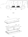
FIG. 1 is a structural diagram of a vehicle in embodiments of the present application; -
FIG. 2 is a structural diagram of a battery group inFIG. 1 ; -
FIG. 3 is a structural diagram of a battery module inFIG. 2 ; -
FIG. 4 andFIG. 5 are a schematic diagram of an exploded structure of a connecting assembly inFIG. 3 ; -
FIG. 6 is an enlarged structural diagram of part M inFIG. 5 ; -
FIG. 7 is a structural diagram of a sampling assembly inFIG. 5 ; -
FIG. 8 is an enlarged structural diagram of part A inFIG. 7 ; -
FIG. 9 is an enlarged structural diagram of part B inFIG. 7 ; -
FIG. 10 is an enlarged structural diagram of part C inFIG. 7 ; -
FIG. 11 is an enlarged structural diagram of part D inFIG. 7 ; -
FIG. 12 is a top view structural diagram of a connecting assembly inFIG. 3 ; -
FIG. 13 is a structural diagram of a G-G section view inFIG. 12 ; -
FIG. 14 is a structural diagram of a J-J section view inFIG. 12 ; -
FIG. 15 is a structural diagram of a I-I section view inFIG. 12 ; -
FIG. 16 is a bottom view structural diagram of a connecting assembly inFIG. 3 ; -
FIG. 17 is a structural diagram of a first insulating film inFIG. 4 ; -
FIG. 18 is an enlarged structural diagram of part E inFIG. 17 ; -
FIG. 19 is an enlarged structural diagram of part K inFIG. 17 ; -
FIG. 20 is a structural diagram of a second insulating film inFIG. 4 ; -
FIG. 21 is an enlarged structural diagram of part F inFIG. 20 . - The reference signs of each drawing respectively denote:
- 1, connecting assembly;
- 11, connecting sheet;
- 12, first insulating film; 121, first insulating film through hole;
- 13, second insulating film; 131, second insulating film through hole;
- 14, sampling assembly; 141, circuit board; 1411, connecting portion; 1412, first circuit board through hole; 1412a, first transverse section groove; 1412b, longitudinal section groove; 1412c, second transverse section groove; 1413, first groove; 1414, gap; 1415, second groove; 1416, connecting neck; 142; sampling terminal;
- 2, end plate;
- 3, insulating cover;
- 4, battery cell; 41, positive electrode lead; 42, negative electrode lead;
- 5, first lace;
- 6, second lace;
- 10, battery module;
- 20, upper box body;
- 30, lower box body;
- 100, battery group;
- 200, vehicle body;
- P, first segment; Q, second segment.
- X1, a length direction of a battery module; Y1, a width direction of a battery module, Z1, a height direction of a battery module;
- X2, a length direction of a connecting assembly; Y2, a width direction of a connecting assembly; Z2, a height direction of a connecting assembly;
- X3, a longitudinal direction of a circuit board; Y3, a transverse direction of a circuit board;
- a, a width of a narrow insulating film through hole;
- b, a width of a wide insulating film through hole;
- c, a distance between hole walls disposed close to a first insulating film through hole and a second insulating film through hole;
- d, a width of a first insulating film through hole;
- e, a width of a second insulating film through hole;
- f, a distance between a second transverse section and a connecting portion; and
- h, a distance between a first transverse section and a connecting portion;
- The following clearly and completely describes the technical solutions in the embodiments of the present application with reference to the drawings in the embodiments of the present application. Apparently, the described embodiments are merely some but not all of the embodiments of the present application. The following description on the at least one exemplary embodiment is actually illustrative only, but not to make any limitation to the present application and its application or use. All other embodiments obtained by a person of ordinary skill in the art based on the embodiments of the present application without creative efforts shall fall within the protection scope of the present application.
- Unless otherwise described additionally and specifically, the components, relative arrangement of steps, number expressions and values as described in these embodiments do not constitute any limitation to the scope of the present application. Meanwhile, it should be understood that to facilitate description, a size of each part shown in the drawings is not drawn according to an actual proportional relationship. A technique, method and device known for a person of ordinary skill in the art is not likely to be discussed in details. However, at an appropriate situation, the technique, method and device should be regarded as a part of the granted description. Of all examples shown and discussed herein, any specific value should be interpreted as only exemplary, but not to serve as a limitation. Therefore, other examples of exemplary embodiments may have different values. It should be noted that similar markers and letters denote similar items in the drawings below. Therefore, once one item is defined in one drawing, it does not need to be further discussed in a subsequent drawing.
- To facilitate description, relative terms of space can be used herein, such as "above ...", "over...", "on an upper surface of ..." and "upper" etc., which are used for describing a spatial positional relationship of one device or characteristic shown in the drawings with other devices or characteristics. It should be understood that relative terms of space aim to include different orientations in use or operation other than orientations of a device described in the drawing. For example, if a device in an drawing is inverted, the device after being described as "above other element or structure" or "over other device or structure" is located as "below other device or structure" or "under other device or structure". Thus, exemplary terms "above..." may include two orientations: "above ..." and "below ...". The device can also be defined in other different manners and corresponding interpretations are made to relative description of space used herein.
- In the following, the structure of the battery module in embodiments of the present application, and the structure of the connecting assembly in the embodiments are described in details according to
FIG. 1 to FIG. 21 . - Embodiments of the present application provide a device using a
battery module 10 as a power supply, abattery group 100, abattery module 10 and a connecting assembly 1. The device using abattery module 10 as a power supply includes abattery module 10 and a driving apparatus for providing a driving force to the device, and thebattery module 10 provides electrical energy to the driving apparatus. The driving force of the device can all be electrical energy and can be partially electrical energy and partially other energy (for example mechanic energy). For example, the device can further include an engine and other power source that provides mechanic energy. A device is within the protection scope of the present application as long as the device uses thebattery module 10 as a power supply. - The device in embodiments of the present application can be a vehicle, a ship, a small aircraft, and other mobile devices. With a vehicle as an example, the vehicle in embodiments of the present application can be a new energy vehicle. The new energy vehicle can be a pure electric vehicle or can be a hybrid power vehicle or an extended-range vehicle etc. As shown in
FIG. 1 , the vehicle includes abattery group 100 and avehicle body 200, where thebattery group 100 is disposed in thevehicle body 200, and includes at least onebattery module 10. Thevehicle body 200 is provided with a driving motor, which is electrically connected to thebattery group 100. Thebattery group 100 provides electric energy for the driving motor. The driving motor is connected through a transmission mechanism to wheels on thevehicle body 200 so as to drive the vehicle to travel ahead. Specifically, thebattery group 100 can be horizontally disposed at bottom of thevehicle body 200. - The
battery module 100 in embodiments of the present application includes at least onebattery module 10. Specifically in the embodiments, as shown inFIG. 2 , thebattery group 100 in the embodiments includes a plurality ofbattery modules 10 and a box body for accommodating the plurality ofbattery modules 10. The box body is provided with an accommodating cavity, and the plurality ofbattery modules 10 are arranged in the accommodating cavity. Specifically, the box body in the embodiments is a box-shaped box body and includes alower box body 30 which accommodates thebattery module 10 and anupper box body 20 which covers thelower box body 30. In embodiments not shown in other drawings, the box body can also be a frame-shaped box body, a disk- shaped box body or other shapes of box body. - As shown in
FIG. 3 , thebattery module 10 in embodiments of the present application includes a plurality ofbattery cells 4 and a frame structure for fixing the plurality ofbattery cells 4. The plurality ofbattery cells 4 are stacked and arranged in a row along the length direction X1. The frame structure includes anend plate 2, afirst lace 5 and a second lace 6, where theend plate 2 is located at two ends on the length direction X1 of thebattery module 10, and theend plate 2 is configured to limit movement of thebattery cells 4 along the length direction X1 of thebattery module 10. Thefirst lace 5 and the second lace 6 are configured to connect the plurality of stackedbattery cells 4. - In embodiments not shown in other drawings, the frame structure may further include side plates located at two sides on the width direction Y1 of the battery module, the side plates are connected to the end plate and enclosed to form the frame structure. In addition, the
battery module 10 may not be provided with a frame structure. When thebattery module 10 is fixed into the box body of thebattery group 100, the plurality of stackedbattery cells 4 are fixed through a skeleton structure of the box body, such as side of the box body, reinforcing beams and the like; or thebattery cells 4 can be further fixed to the box body through bonding or other manners. - The
battery module 10 in the embodiments further includes an insulatingcover 3, which is disposed between the frame structure and thebattery cells 4 to perform a function of insulation. Specifically, in the embodiments, the insulatingcover 3 is located between theend plate 2 and thebattery cells 4, and between the lace and thebattery cells 4. - The
battery cell 4 in the embodiments includes an electrode lead. Specifically, each of thebattery cells 4 includes apositive electrode lead 41 and anegative electrode lead 42. In thebattery module 10, the plurality ofbattery cells 4 are electrically connected in manners like series and/or parallel etc. Moreover, theadjacent battery cells 4 are connected through a connectingsheet 11. For example, when thebattery cells 4 are connected in series, thepositive electrode lead 41 of onebattery cell 4 is connected to thenegative electrode lead 42 of anotherbattery cell 4 through the connectingsheet 11; or when thebattery cells 4 are connected in parallel, thepositive electrode lead 41 of onebattery cell 4 is connected to thepositive electrode lead 41 of anotherbattery cell 4 through the connectingsheet 11. - As shown in
FIG. 3 to FIG. 5 , the connecting assembly 1 in the embodiments includes a plurality of connectingsheets 11, asampling assembly 14 and an insulating film, where thesampling assembly 14 includes acircuit board 141 and asampling terminal 142 connected to thecircuit board 141, thesampling terminal 142 is connected to the plurality of connectingsheets 11, the insulating film is provided at one side of thesampling assembly 14 and the plurality of connectingsheets 11, and the insulating film connects thesampling assembly 14 and the plurality of connectingsheets 11 to form an integral structure with thesampling assembly 14 and the plurality of connectingsheets 11, thus improving assembling efficiency of thebattery module 10. An insulating film through hole is provided in a region of thesampling assembly 14 covered by the insulating film. In the manufacturing process of thebattery module 10, when the connectingsheets 11 of the connecting assembly 1 are connected to an electrode lead of thebattery cells 4, there may be a deviation between the connectingsheets 11 and the electrode lead due to a manufacturing error, such that the connectingsheets 11 stretch thesampling assembly 14 connected to it. In this case, it is extremely easy to cause a failure of connection between the connectingsheets 11 and thesampling assembly 14 or to cause thesampling assembly 14 itself to be fractured, resulting in failed sampling and even tearing off the insulating film, which causes a connection failure of the connectingassembly 11. By providing the insulating film through hole, thesampling assembly 14 is made to have an activity space, which can avoid failed sampling caused by a manufacturing error. In the manufacturing process of thebattery module 10, thebattery cells 4 expand after charging and discharging many times, causing a relative displacement between thebattery cells 4, and the insulating film through hole provided on the insulating film can also release an expansion force to prevent the insulating film from being torn off and sampling failure, thereby improving the safety of the battery module. - The
sampling assembly 14 and the plurality of connectingsheets 11 in the embodiments are integrated into one by bonding the insulating films, hot pressing or injection molding process, to facilitate assembling of thebattery module 10 so as to improve production efficiency. In some embodiments, thesampling assembly 14 and the plurality of connectingsheets 11 are integrated into one by hot pressing insulating films to facilitate manufacturing of the connecting assembly 1. - Specifically, in the embodiments, the
circuit board 141 can be FPC, PCB and FFC etc. Thecircuit board 141 is composed of a sampling line and an insulating material that wraps the sampling line. Thesampling terminal 142 can be a nickel sheet, a copper sheet and an aluminum sheet etc. connected to the sampling line in thecircuit board 141. Thesampling terminal 142 can also be a part of the sampling line inside thecircuit board 141 that extends out. Specific limitations are not made herein, as long as collection of information of thebattery cells 4 can be implemented. The specific sampling line is electrically connected to thesampling terminal 142 to realize a sampling function. In some embodiments, thecircuit board 141 is a flexible circuit board, such as FPC; and thesampling terminal 142 is a nickel sheet. The flexible circuit board is flexible and small in volume such that internal space can be saved for the assembledbattery module 10. - After the
sampling assembly 14 and the plurality of connectingsheets 11 are integrated by hot pressing the insulating film, a position of thecircuit board 141 is restricted and cannot move, resulting in an increase in the rigidity of the entire connecting assembly 1. So when expansion occurs to thebattery module 10, it is easy for thecircuit board 141 to stretch under the expansion force, thus causing failure of an electrical connection of the sampling line inside thecircuit board 141. In order to reduce rigidity of the entire connecting assembly 1 to avoid sampling failure, as shown inFIG. 7 to FIG. 11 , thecircuit board 141 of the embodiments is provided with a circuit board opening, and a position of the insulating film through hole corresponds to a position of the circuit board opening. - As shown in
FIG. 8 , thecircuit board 141 is provided with a connectingportion 1411 connected to thesampling terminal 142, and the circuit board opening is disposed close to the connectingportion 1411. Thesampling terminal 142 is connected to the connectingsheets 11. The connectingsheets 11 are connected to an electrode lead of thebattery cells 4. Therefore, when thebattery cells 4 are deformed upon charging and discharging, the connectingportion 1411 connecting thecircuit board 141 to thesampling terminal 142 is a place where the force is applied. Thus, disposing the circuit board opening close to the connectingportion 1411 can better increase flexibility of the connecting assembly 1 close to the connectingportion 1411 When thecircuit board 141 in the embodiments is vibrated, since the circuit board opening is provided on thecircuit board 141, thecircuit board 141 in the embodiments can absorb vibration of thecircuit board 141 through deformation, thus ensuring connecting strength between the connectingportion 1411 and thesampling terminal 142. - As shown in
FIG. 7 , at different locations at two sides of thecircuit board 141, a plurality ofsampling terminals 142 which are disposed at an interval are connected. As shown inFIG. 8 to FIG. 11 , for thesampling terminal 142 at different locations, the shape of the circuit board opening is substantially the same. According to the internal wiring of thecircuit board 141, the direction of the circuit board opening can be properly adjusted. The structure of the circuit board opening at part A inFIG. 7 is described in details according toFIG. 8 . Circuit board openings at part B, part C and part D ofFIG. 7 are all obtained by the circuit board opening at part A through a certain rotational symmetry. Therefore, the structure can refer to the structure of the circuit board opening at part A can be referred to and it is not repeated herein. - As shown in
FIG. 8 , thecircuit board 141 in the embodiments includes a connectingneck 1416 located at one side of the connectingportion 1411, and the interior of the connectingneck 1416 is provided with a sampling line. - In the embodiments, the circuit board opening includes a circuit board through
hole 1412 passing through thecircuit board 141 and afirst groove 1413 formed by a side of thecircuit board 141 being recessed inward, the circuit board throughhole 1412 includes a firsttransverse section 1412a extending along a transverse direction Y3 of thecircuit board 141, thefirst groove 1413 is located in an extending direction of the firsttransverse section 1412a and has agap 1414 with the firsttransverse section 1412a. Before thecircuit board 141 and the insulating film are hot pressed, agap 1414 exists between the firsttransverse section 1412a and thefirst groove 1413, thus facilitating bonding between thecircuit board 141 and the insulating film and facilitating flattening of the insulating film and the fixing of thesampling terminal 142 in the hot pressing process, thus improving production efficiency. When thesampling terminal 142 is deformed with the expansion of thebattery cells 4, thesampling terminal 142 applies an acting force to thecircuit board 141. With the increase of the acting force, thegap 1414 between thefirst groove 1413 and the firsttransverse section 1412a will be broken, thus making the connectingneck 1416 into a cantilever structure, resulting in easier deformation. The interior of thegap 1414 may be provided with a sampling line or may not be provided with a sampling line. When the sampling line is provided inside thegap 1414, the sampling line inside thegap 1414 is in a parallel relationship with the sampling line inside the connectingneck 1416. When the sampling line inside thegap 1414 is broken, the sampling line inside the connectingneck 1416 can also perform a sampling function. In some embodiments, the sampling line is not provided inside thegap 1414, which can reduce wiring difficulty of the sampling line inside thecircuit board 141 and reduce cost. - Specifically, the first
transverse section 1412a and thefirst groove 1413 of the embodiments are both provided narrowly, such that thegap 1414 is also narrow and easy to break under effect of thesampling terminal 142. - The circuit board through
hole 1412 in the embodiments further includes alongitudinal section 1412b extending along a longitudinal direction X3 of thecircuit board 141, and the firsttransverse section 1412a is located at a first end of the longitudinal section1412b and communicates to thelongitudinal section 1412b. The arrangement of thelongitudinal section 1412b enables increase of the flexibility of thecircuit board 141 in the embodiments. - In order to further improve flexibility of the
circuit board 141, the circuit board throughhole 1412 in the embodiments further includes a secondtransverse section 1412c extending along a transverse direction Y3 of thecircuit board 141, and the secondtransverse section 1412c is located at a second end of thelongitudinal section 1412b and communicates to thelongitudinal section 1412b. - Referring to size marking in
FIG. 10 , in the longitudinal direction X3 of thecircuit board 141, a distance f between the secondtransverse section 1412c and the connectingportion 1411 is greater than a distance h between the firsttransverse section 1412a and the connectingportion 1411. Providing in such a manner enables length of the connectingneck 1416 longer, which is advantageous to deformation of thecircuit board 141. - In some embodiments, the circuit board opening further includes a
second groove 1415 formed by a side of thecircuit board 141 being recessed inward, and thesecond groove 1415 and thefirst groove 1413 are respectively located at two sides of the connectingportion 1411. The arrangement of thesecond groove 1415 enables easier deformation of thecircuit board 141 when the connectingportion 1411 is under force, thus ensuring connecting stability between thesampling terminal 142 and the connectingportion 1411. - In the longitudinal direction X3 of the
circuit board 141, thesecond groove 1415 and the secondtransverse section 1412c are disposed in a misalignment manner, thus reserving sufficient locations for internal wiring of thecircuit board 141 and improving connecting strength of the connectingneck 1416. - It needs to be noted therein that the length direction X3 of the
circuit board 141 in the embodiments is consistent with the length direction X1 of thebattery module 10, which relates to arrangement of thebattery cells 4 in thebattery module 10. In embodiments not shown in other drawings, the longitudinal direction X3 of the circuit board can also be inconsistent with the length direction X1 of the battery module. - In order to further improve strength and connecting reliability of the connecting assembly 1, as shown in
FIG. 4 andFIG. 5 , the insulating film of the embodiments includes a first insulatingfilm 12 and a second insulatingfilm 13 that are respectively attached to two sides of thesampling assembly 14 and the plurality of connectingsheets 11, that is, thesampling assembly 14 and the plurality of connectingsheets 11 are located between the first insulatingfilm 12 and the second insulatingfilm 13. Specifically, thesampling assembly 14 and the plurality of connectingsheets 11 in the embodiments are hot-pressed and integrated into one with the first insulatingfilm 12 and the second insulatingfilm 13. In the height direction Z2 of the connecting assembly 1, the first insulatingfilm 12 is located at an upper side and the second insulatingfilm 13 is located at a lower side. - In order to prevent the insulating film from being torn off when the
sampling assembly 14 and the plurality of connectingsheets 11 are being deformed, the first insulatingfilm 12 and the second insulatingfilm 13 in the embodiments are both provided with insulating film through holes. Specifically, as shown inFIG. 12 andFIG. 17 , the first insulatingfilm 12 is provided with a first insulating film throughhole 121. As shown inFIG. 16 andFIG. 20 , the second insulatingfilm 13 is provided with a second insulating film throughhole 131. - As shown in
FIG. 18, FIG. 19 andFIG. 21 , a position of the insulating film through hole in the embodiments is disposed in correspondence to a position of the circuit board opening, the insulating film through hole includes a first segment P corresponding to the position of the circuit board throughhole 1412 and a second segment Q extending from a position corresponding to thesecond groove 1415 to a position corresponding to thefirst groove 1413. A position of the insulating film through hole in the embodiments is in correspondence to a position of the circuit board opening, such that after the insulating film and thecircuit board 141 are connected into one, a cantilever structure is formed with a part of thecircuit board 141 close to thesampling terminal 142, which is advantageous to deformation. - Since the first insulating
film 12 and the second insulatingfilm 13 in the embodiments are both provided with insulating film through holes and thecircuit board 141 is also provided with a circuit board opening at a corresponding location, in order to avoid a metal particle falling inside thebattery module 10 through the insulating film through holes and the circuit board opening to cause a short circuit, in one embodiment, as shown inFIG. 13 and FIG. 14 , a position of the first insulating film throughhole 121 and a position of the second insulating film throughhole 131 are opposite, and a width of one insulating film through hole of the first insulating film throughhole 121 and the second insulating film through hole131 is smaller than a width of the other insulating film through hole of the first insulating film throughhole 121 and the second insulating film through hole131. That is, one of the first insulating film throughhole 121 and the second insulating film through hole131 is a narrow insulating film through hole and the other of the first insulating film throughhole 121 and the second insulating film throughhole 131 is a wide insulating film through hole. Specifically, as shown inFIG. 13 , the first insulating film throughhole 121 is a narrow insulating film through hole. As shown inFIG. 14 , the second insulating film throughhole 131 is a wide insulating film through hole. After the first insulatingfilm 12 and the second insulatingfilm 13 are molded integrally with thesampling assembly 14 by hot pressing, the whole connection assembly 1 performs a function of blocking the metal particle is the narrow insulating film through hole. - In order to enable the insulating film through hole to further prevent the metal particle falling inside the
battery module 10 on the basis of releasing the expansion force, a width a of the narrow insulating film through hole in the embodiments is in a range of [0, 0.5mm]. In some embodiments, the width a of the narrow insulating film through hole is smaller than or equal to 0.2mm, thus achieving better effects in preventing the metal particle falling inside thebattery module 10. - As shown in
FIG. 13 and FIG. 14 , a width of the circuit board opening in the embodiment is the same as a width of the wide insulating film through hole. In order to improve material utilization ratio of thecircuit board 141 and help to release the expansion force, and further ensure a sufficient bonding area of the insulating film and thecircuit board 141 on the basis of improving service life of the mold, a width b of the wide insulating film through hole in the embodiment is in a range of [0.5mm, 3mm]. In some embodiments, when the width b of the wide insulating film through hole is 1mm, the bonding area of the insulating film and thecircuit board 141 is larger and the material utilization ratio of thecircuit board 141 is also higher. - In order to avoid a metal particle falling inside the
battery module 10 through the insulating film through hole and the circuit board opening to cause a short circuit, in another one embodiment, as shown inFIG. 15 , the first insulating film throughhole 121 and the second insulating film throughhole 131 are disposed in a misalignment manner. Since the first insulating film throughhole 121 and the second insulating film throughhole 131 are misaligned, after the first insulatingfilm 12, thecircuit board 141 and the second insulatingfilm 13 are hot pressed, it can prevent the metal particle falling inside thebattery module 10 through the connecting assembly 1. - As shown in
FIG. 15 , a width of the first insulating film throughhole 121 in the embodiment is d and a width of the second insulating film throughhole 131 is e. In the embodiment, the width d of the first insulating film throughhole 121 is the same as the width e of the second insulating film throughhole 131. Moreover, in order to improve the material utilization ratio of thecircuit board 141 and ensure a sufficient bonding area of the insulating film and thecircuit board 141, the width d of the first insulating film throughhole 121 and the width e of the second insulating film throughhole 131 in the embodiment have a range of [0.5mm, 3mm]. In some embodiments, the width d of the first insulating film throughhole 121 and the width e of the second insulating film throughhole 131 are both 1mm. - In other embodiments, the width d of the first insulating film through
hole 121 and the width e of the second insulating film throughhole 131 may not be the same either. - In order to prevent the metal particle falling inside the module, a distance between hole walls disposed close to a first insulating film through
hole 121 and a second insulating film throughhole 131 in the embodiment is greater than or equal to -0.5mm. At this time, the connecting assembly 1 still has an opening within 0.5mm after being hot pressed. The metal particle within 0.5mm can still fall inside thebattery module 10 through the opening. That is, when c is greater than or equal to -0.5mm, it can prevent most metal particles falling inside thebattery module 10. In order to prevent the metal particle falling inside thebattery module 10 better, a distance c between hole walls disposed close to a first insulating film throughhole 121 and a second insulating film throughhole 131 in the embodiment is in a range of [-0.5mm, 3mm]. In some embodiments, when a distance c between hole walls disposed close to a first insulating film throughhole 121 and a second insulating film throughhole 131 is 0.5mm, the effects of the insulating film in preventing the metal particle falling inside in the embodiment and the effects of releasing the expansion force are better. - In some embodiments, in order to prevent stress concentration, as shown in
FIG. 18, FIG. 19 andFIG. 21 , end portions and corners of the insulating film through hole are transitioned with circular corners to prevent stress concentration. - Finally, it should be noted that the foregoing embodiments are merely intended to describe the technical solutions of the present application, but not intended to constitute any limitation. Although the present application is described in detail with reference to preferred embodiments, a person of ordinary skill in the art should understand that modifications or equivalent replacements of partial technical features can still be made to the specific embodiments of the present application, without departing from the spirit of the technical solutions of the present application, and shall fall within the scope of the technical solutions sought for protection in the present application.
Claims (17)
- A connecting assembly for a battery module, comprising:a plurality of connecting sheets (11) configured to connect battery cells (4) of the battery module;a sampling assembly (14) comprising a circuit board (141) and a sampling terminal (142) connected to the circuit board (141), the sampling terminal (142) being connected to the plurality of connecting sheets (11); andan insulating film disposed at one side of the sampling assembly (14) and the plurality of connecting sheets (11), and the insulating film connecting the sampling assembly (14) and the plurality of connecting sheets (11) to form an integral structure with the sampling assembly (14) and the plurality of connecting sheets (11), and an insulating film through hole being provided in a region of the sampling assembly (14) covered by the insulating film.
- The connecting assembly according to claim 1, wherein the circuit board (141) is provided with a circuit board opening, and a position of the insulating film through hole corresponds to a position of the circuit board opening.
- The connecting assembly according to claim 2, wherein the circuit board (141) is provided with a connecting portion (1411) connected to the sampling terminal (142), and the circuit board opening is disposed close to the connecting portion (1411).
- The connecting assembly according to claim 3, wherein the circuit board opening comprises a circuit board through hole (1412) passing through the circuit board (141) and a first groove (1413) formed by a side of the circuit board (141) being recessed inward, the circuit board through hole (1412) comprises a first transverse section (1412a) extending along a transverse direction (Y3) of the circuit board, and the first groove (1413) is located in an extending direction of the first transverse section (1412a) and has a gap (1414) with the first transverse section (1412a).
- The connecting assembly according to claim 4, wherein the circuit board through hole (1412) further comprises a longitudinal section (1412b) extending along a longitudinal direction (X3) of the circuit board, and the first transverse section (1412a) is located at a first end of the longitudinal section (1412b) and communicates to the longitudinal section (1412b).
- The connecting assembly according to claim 5, wherein the circuit board through hole (1412) further comprises a second transverse section (1412c) extending along the transverse direction (Y3) of the circuit board, and the second transverse section (1412c) is located at a second end of the longitudinal section (1412b) and communicates to the longitudinal section (1412b).
- The connecting assembly according to claim 6, wherein on the longitudinal direction (X3) of the circuit board, a distance (f) between the second transverse section (1412c) and the connecting portion (1411) is greater than a distance (h) between the first transverse section (1412a) and the connecting portion (1411).
- The connecting assembly according to claim 7, wherein the circuit board opening further comprises a second groove (1415) formed by a side of the circuit board (141) being recessed inward, and the second groove (1415) and the first groove (1413) are respectively located at two sides of the connecting portion (1411).
- The connecting assembly according to claim 8, wherein a position of the insulating film through hole is disposed in correspondence to a position of the circuit board opening, and the insulating film through hole comprises a first segment (P) corresponding to a position of the circuit board through hole (1412) and a second segment (Q) extending from a position corresponding to the second groove (1415) to a position corresponding to the first groove (1413).
- The connecting assembly according to any one of claims 1 to 9, wherein the insulating film comprises a first insulating film (12) and a second insulating film (13) that are respectively attached to two sides of the sampling assembly (14) and the plurality of connecting sheets (11), the first insulating film (12) is provided with a first insulating film through hole (121) and the second insulating film (13) is provided with a second insulating film through hole (131).
- The connecting assembly according to claim 10, wherein the first insulating film through hole (121) and the second insulating film through hole (131) are disposed in a misalignment manner.
- The connecting assembly according to claim 11, wherein a distance range between hole walls disposed close to the first insulating film through hole (121) and the second insulating film through hole (131) is [-0.5mm, 3mm].
- The connecting assembly according to claim 10, wherein a position of the first insulating film through hole (121) and a position of the second insulating film through hole (131) are opposite, a width of one insulating film through hole of the first insulating film through hole (121) and the second insulating film through hole (131) is smaller than a width of the other insulating film through hole.
- The connecting assembly according to claim 13, wherein a width a of a narrow insulating film through hole of the first insulating film through hole (121) and the second insulating film through hole (131) is in a range of [0mm, 0.5mm] and a width b of a wide insulating film through hole of the first insulating film through hole (121) and the second insulating film through hole (131) is in a range of [0.5mm, 3mm].
- A battery module comprising a plurality of battery cells (4) disposed in a stack manner and the connecting assembly (1) according to any one of claims 1 to 14, wherein the plurality of connecting sheets (11) are connected to an electrode lead of the plurality of battery cells (4).
- A battery group comprising a box body and the battery module (10) according to claim 15, wherein the battery module (10) is accommodated in the box body.
- A device using a battery module as a power supply comprising a driving apparatus and the battery module (10) according to claim 15, wherein the driving apparatus is configured to provide a driving force to the device, and the battery module (10) is configured to provide electrical energy to the driving apparatus.
Applications Claiming Priority (2)
| Application Number | Priority Date | Filing Date | Title |
|---|---|---|---|
| CN201910999593.XA CN112310567B (en) | 2019-10-21 | 2019-10-21 | Connection assembly, battery module, battery pack, and apparatus using battery module as power source |
| PCT/CN2020/121719 WO2021078078A1 (en) | 2019-10-21 | 2020-10-17 | Connecting assembly, battery module, battery pack, and device using battery module as power source |
Publications (4)
| Publication Number | Publication Date |
|---|---|
| EP3923408A1 true EP3923408A1 (en) | 2021-12-15 |
| EP3923408A4 EP3923408A4 (en) | 2022-06-15 |
| EP3923408B1 EP3923408B1 (en) | 2024-02-07 |
| EP3923408C0 EP3923408C0 (en) | 2024-02-07 |
Family
ID=74485589
Family Applications (1)
| Application Number | Title | Priority Date | Filing Date |
|---|---|---|---|
| EP20880133.2A Active EP3923408B1 (en) | 2019-10-21 | 2020-10-17 | Connecting assembly, battery module, battery pack, and device using battery module as power source |
Country Status (6)
| Country | Link |
|---|---|
| US (1) | US11764444B2 (en) |
| EP (1) | EP3923408B1 (en) |
| JP (1) | JP7403642B2 (en) |
| KR (1) | KR20220068237A (en) |
| CN (1) | CN112310567B (en) |
| WO (1) | WO2021078078A1 (en) |
Families Citing this family (4)
| Publication number | Priority date | Publication date | Assignee | Title |
|---|---|---|---|---|
| CN112310520A (en) * | 2019-10-21 | 2021-02-02 | 宁德时代新能源科技股份有限公司 | Connecting assembly, battery module, battery pack and device |
| CN113782917A (en) * | 2021-09-28 | 2021-12-10 | 东莞新能安科技有限公司 | Connecting piece, group battery and consumer |
| CN216903165U (en) * | 2022-01-27 | 2022-07-05 | 宁德时代新能源科技股份有限公司 | Flexible circuit board assembly, battery and electric device |
| KR20240031710A (en) | 2022-09-01 | 2024-03-08 | 한국단자공업 주식회사 | battery cell connecting apparatus |
Family Cites Families (29)
| Publication number | Priority date | Publication date | Assignee | Title |
|---|---|---|---|---|
| CN102197509B (en) * | 2008-09-09 | 2014-11-26 | 江森自控帅福得先进能源动力系统有限责任公司 | Interconnection washer assembly for a battery assembly |
| KR101030856B1 (en) * | 2008-12-16 | 2011-04-22 | 삼성에스디아이 주식회사 | Battery pack |
| JP2010257750A (en) * | 2009-04-24 | 2010-11-11 | Sanyo Electric Co Ltd | Battery module, battery system, and electric vehicle |
| DE102010005017A1 (en) * | 2010-01-19 | 2011-07-21 | Li-Tec Battery GmbH, 01917 | Electric power unit and spacer |
| CN102544616B (en) * | 2010-12-08 | 2014-07-30 | 比亚迪股份有限公司 | Battery module |
| DE102011016373A1 (en) * | 2011-04-07 | 2012-10-11 | Intedis Gmbh & Co. Kg | Battery block for use as energy storage in motor car, has contact elements provided at circuit board in sections, and monitoring and balancing circuits in contact with power connector at battery cells on circuit board via contact elements |
| US8609276B2 (en) * | 2011-06-23 | 2013-12-17 | Samsung Sdi Co., Ltd. | Battery pack |
| JP6138688B2 (en) * | 2011-08-26 | 2017-05-31 | 三洋電機株式会社 | Power supply device, vehicle including the same, and power storage device |
| CN203134923U (en) * | 2013-03-23 | 2013-08-14 | 广州安费诺诚信软性电路有限公司 | Aluminum-copper combined electrode flexible circuit board for battery monitor |
| JP6148555B2 (en) | 2013-07-16 | 2017-06-14 | 株式会社ジーエスエレテック | Busbar module device |
| US20150044511A1 (en) * | 2013-08-08 | 2015-02-12 | Samsung Sdi Co., Ltd. | Battery pack |
| JP6451650B2 (en) * | 2014-01-17 | 2019-01-16 | 三洋電機株式会社 | Power supply |
| CN204029949U (en) * | 2014-06-30 | 2014-12-17 | 深圳市比亚迪锂电池有限公司 | A kind of signal acquisition module of electrokinetic cell module and electrokinetic cell |
| CN204029950U (en) * | 2014-06-30 | 2014-12-17 | 比亚迪股份有限公司 | A kind of signal acquisition module of electrokinetic cell module and electrokinetic cell module |
| CN104795518A (en) * | 2015-03-20 | 2015-07-22 | 飞天诚信科技股份有限公司 | Battery and electronic equipment containing battery |
| CN106328875A (en) * | 2015-06-29 | 2017-01-11 | 深圳市沃特玛电池有限公司 | Safety structure of battery pack connection board |
| CN206022485U (en) * | 2016-09-09 | 2017-03-15 | 深圳市沃特玛电池有限公司 | A kind of battery modules |
| JP6227082B1 (en) * | 2016-10-03 | 2017-11-08 | 株式会社オートネットワーク技術研究所 | Connection module |
| DE102016223464A1 (en) * | 2016-11-25 | 2018-05-30 | Robert Bosch Gmbh | Connecting device for the electrical connection of electrical storage units |
| US10720626B2 (en) * | 2016-12-29 | 2020-07-21 | Romeo Systems, Inc. | Systems and methods for battery structure, interconnects, sensing, and balancing |
| KR102169631B1 (en) * | 2017-03-21 | 2020-10-23 | 주식회사 엘지화학 | Battery module, battery pack comprising the battery module and vehicle comprising the battery pack |
| CN206878083U (en) * | 2017-06-23 | 2018-01-12 | 宁德时代新能源科技股份有限公司 | Battery modules |
| CN107785526A (en) * | 2017-09-29 | 2018-03-09 | 苏州西典机电有限公司 | Electrokinetic cell integration module |
| CN109103405A (en) * | 2018-08-19 | 2018-12-28 | 江西赣锋电池科技有限公司 | A kind of battery pack busbar, preparation method and battery pack |
| CN209087964U (en) * | 2018-09-13 | 2019-07-09 | 东莞市硅翔绝缘材料有限公司 | A kind of integrated busbar of battery modules FPCA control circuit |
| CN209087963U (en) * | 2018-09-13 | 2019-07-09 | 东莞市硅翔绝缘材料有限公司 | A kind of integrated busbar of battery modules PCBA control circuit |
| CN210744068U (en) * | 2019-10-21 | 2020-06-12 | 宁德时代新能源科技股份有限公司 | Connecting assembly, battery module, battery pack and device |
| CN210744018U (en) * | 2019-10-21 | 2020-06-12 | 宁德时代新能源科技股份有限公司 | Connecting assembly, battery module, battery pack and device |
| CN211045640U (en) * | 2019-10-22 | 2020-07-17 | 中航光电科技股份有限公司 | Full-coated film-pasted wire harness board assembly and battery module |
-
2019
- 2019-10-21 CN CN201910999593.XA patent/CN112310567B/en active Active
-
2020
- 2020-10-17 EP EP20880133.2A patent/EP3923408B1/en active Active
- 2020-10-17 JP JP2022523330A patent/JP7403642B2/en active Active
- 2020-10-17 WO PCT/CN2020/121719 patent/WO2021078078A1/en unknown
- 2020-10-17 KR KR1020227012841A patent/KR20220068237A/en not_active Application Discontinuation
-
2021
- 2021-12-28 US US17/564,012 patent/US11764444B2/en active Active
Also Published As
| Publication number | Publication date |
|---|---|
| EP3923408B1 (en) | 2024-02-07 |
| CN112310567B (en) | 2022-03-18 |
| US11764444B2 (en) | 2023-09-19 |
| US20220123442A1 (en) | 2022-04-21 |
| JP2022552725A (en) | 2022-12-19 |
| WO2021078078A1 (en) | 2021-04-29 |
| EP3923408A4 (en) | 2022-06-15 |
| JP7403642B2 (en) | 2023-12-22 |
| EP3923408C0 (en) | 2024-02-07 |
| KR20220068237A (en) | 2022-05-25 |
| CN112310567A (en) | 2021-02-02 |
Similar Documents
| Publication | Publication Date | Title |
|---|---|---|
| EP3923408A1 (en) | Connecting assembly, battery module, battery pack, and device using battery module as power source | |
| US10361463B2 (en) | Battery module having improved fastening structure | |
| CN100446306C (en) | Rechargeable battery module | |
| US11858332B2 (en) | Battery, power consumption apparatus, and method for producing battery | |
| US11843129B2 (en) | Connecting assembly, battery module, battery pack, and device using battery module as power supply | |
| US11942647B2 (en) | Harness isolation plate assembly, battery module, battery pack and device | |
| EP3930086B1 (en) | Battery module, battery pack, and device which uses battery cell as power supply | |
| CN211929598U (en) | Battery monomer, battery and device of power consumption | |
| US11264669B2 (en) | Battery box and battery module | |
| JP7479499B2 (en) | Battery, power consumption device and battery manufacturing method | |
| KR101084986B1 (en) | Middle or Large-sized Battery Pack of Improved Safety | |
| KR101797690B1 (en) | Battery Pack Including Bus Bar Assembly Formed Protrusion Portion for Insulation | |
| JP7532634B2 (en) | Battery cell, battery, power receiving device, and method of manufacturing battery cell | |
| EP4184684A1 (en) | Battery module | |
| CN221262547U (en) | Battery monomer, battery and electric equipment | |
| EP4333157A1 (en) | Battery module | |
| US20240213627A1 (en) | Battery-cell coupling structure | |
| JP4590861B2 (en) | Assembly of battery modules |
Legal Events
| Date | Code | Title | Description |
|---|---|---|---|
| STAA | Information on the status of an ep patent application or granted ep patent |
Free format text: STATUS: THE INTERNATIONAL PUBLICATION HAS BEEN MADE |
|
| PUAI | Public reference made under article 153(3) epc to a published international application that has entered the european phase |
Free format text: ORIGINAL CODE: 0009012 |
|
| STAA | Information on the status of an ep patent application or granted ep patent |
Free format text: STATUS: REQUEST FOR EXAMINATION WAS MADE |
|
| 17P | Request for examination filed |
Effective date: 20210907 |
|
| AK | Designated contracting states |
Kind code of ref document: A1 Designated state(s): AL AT BE BG CH CY CZ DE DK EE ES FI FR GB GR HR HU IE IS IT LI LT LU LV MC MK MT NL NO PL PT RO RS SE SI SK SM TR |
|
| A4 | Supplementary search report drawn up and despatched |
Effective date: 20220518 |
|
| RIC1 | Information provided on ipc code assigned before grant |
Ipc: H01M 50/519 20210101ALI20220512BHEP Ipc: H01M 50/505 20210101ALI20220512BHEP Ipc: H01M 50/531 20210101AFI20220512BHEP |
|
| STAA | Information on the status of an ep patent application or granted ep patent |
Free format text: STATUS: EXAMINATION IS IN PROGRESS |
|
| 17Q | First examination report despatched |
Effective date: 20221010 |
|
| DAV | Request for validation of the european patent (deleted) | ||
| DAX | Request for extension of the european patent (deleted) | ||
| GRAP | Despatch of communication of intention to grant a patent |
Free format text: ORIGINAL CODE: EPIDOSNIGR1 |
|
| STAA | Information on the status of an ep patent application or granted ep patent |
Free format text: STATUS: GRANT OF PATENT IS INTENDED |
|
| RIC1 | Information provided on ipc code assigned before grant |
Ipc: H01M 50/519 20210101ALI20231102BHEP Ipc: H01M 50/505 20210101ALI20231102BHEP Ipc: H01M 50/531 20210101AFI20231102BHEP |
|
| GRAS | Grant fee paid |
Free format text: ORIGINAL CODE: EPIDOSNIGR3 |
|
| INTG | Intention to grant announced |
Effective date: 20231124 |
|
| GRAA | (expected) grant |
Free format text: ORIGINAL CODE: 0009210 |
|
| STAA | Information on the status of an ep patent application or granted ep patent |
Free format text: STATUS: THE PATENT HAS BEEN GRANTED |
|
| RAP3 | Party data changed (applicant data changed or rights of an application transferred) |
Owner name: CONTEMPORARY AMPEREX TECHNOLOGY CO., LIMITED |
|
| AK | Designated contracting states |
Kind code of ref document: B1 Designated state(s): AL AT BE BG CH CY CZ DE DK EE ES FI FR GB GR HR HU IE IS IT LI LT LU LV MC MK MT NL NO PL PT RO RS SE SI SK SM TR |
|
| REG | Reference to a national code |
Ref country code: GB Ref legal event code: FG4D |
|
| REG | Reference to a national code |
Ref country code: CH Ref legal event code: EP |
|
| REG | Reference to a national code |
Ref country code: IE Ref legal event code: FG4D |
|
| REG | Reference to a national code |
Ref country code: DE Ref legal event code: R096 Ref document number: 602020025466 Country of ref document: DE |
|
| U01 | Request for unitary effect filed |
Effective date: 20240301 |
|
| U07 | Unitary effect registered |
Designated state(s): AT BE BG DE DK EE FI FR IT LT LU LV MT NL PT SE SI Effective date: 20240307 |
|
| PG25 | Lapsed in a contracting state [announced via postgrant information from national office to epo] |
Ref country code: IS Free format text: LAPSE BECAUSE OF FAILURE TO SUBMIT A TRANSLATION OF THE DESCRIPTION OR TO PAY THE FEE WITHIN THE PRESCRIBED TIME-LIMIT Effective date: 20240607 |
|
| PG25 | Lapsed in a contracting state [announced via postgrant information from national office to epo] |
Ref country code: GR Free format text: LAPSE BECAUSE OF FAILURE TO SUBMIT A TRANSLATION OF THE DESCRIPTION OR TO PAY THE FEE WITHIN THE PRESCRIBED TIME-LIMIT Effective date: 20240508 |
|
| PG25 | Lapsed in a contracting state [announced via postgrant information from national office to epo] |
Ref country code: HR Free format text: LAPSE BECAUSE OF FAILURE TO SUBMIT A TRANSLATION OF THE DESCRIPTION OR TO PAY THE FEE WITHIN THE PRESCRIBED TIME-LIMIT Effective date: 20240207 Ref country code: RS Free format text: LAPSE BECAUSE OF FAILURE TO SUBMIT A TRANSLATION OF THE DESCRIPTION OR TO PAY THE FEE WITHIN THE PRESCRIBED TIME-LIMIT Effective date: 20240507 |
|
| PG25 | Lapsed in a contracting state [announced via postgrant information from national office to epo] |
Ref country code: ES Free format text: LAPSE BECAUSE OF FAILURE TO SUBMIT A TRANSLATION OF THE DESCRIPTION OR TO PAY THE FEE WITHIN THE PRESCRIBED TIME-LIMIT Effective date: 20240207 |
|
| PG25 | Lapsed in a contracting state [announced via postgrant information from national office to epo] |
Ref country code: RS Free format text: LAPSE BECAUSE OF FAILURE TO SUBMIT A TRANSLATION OF THE DESCRIPTION OR TO PAY THE FEE WITHIN THE PRESCRIBED TIME-LIMIT Effective date: 20240507 Ref country code: NO Free format text: LAPSE BECAUSE OF FAILURE TO SUBMIT A TRANSLATION OF THE DESCRIPTION OR TO PAY THE FEE WITHIN THE PRESCRIBED TIME-LIMIT Effective date: 20240507 Ref country code: IS Free format text: LAPSE BECAUSE OF FAILURE TO SUBMIT A TRANSLATION OF THE DESCRIPTION OR TO PAY THE FEE WITHIN THE PRESCRIBED TIME-LIMIT Effective date: 20240607 Ref country code: HR Free format text: LAPSE BECAUSE OF FAILURE TO SUBMIT A TRANSLATION OF THE DESCRIPTION OR TO PAY THE FEE WITHIN THE PRESCRIBED TIME-LIMIT Effective date: 20240207 Ref country code: GR Free format text: LAPSE BECAUSE OF FAILURE TO SUBMIT A TRANSLATION OF THE DESCRIPTION OR TO PAY THE FEE WITHIN THE PRESCRIBED TIME-LIMIT Effective date: 20240508 Ref country code: ES Free format text: LAPSE BECAUSE OF FAILURE TO SUBMIT A TRANSLATION OF THE DESCRIPTION OR TO PAY THE FEE WITHIN THE PRESCRIBED TIME-LIMIT Effective date: 20240207 |
|
| PG25 | Lapsed in a contracting state [announced via postgrant information from national office to epo] |
Ref country code: PL Free format text: LAPSE BECAUSE OF FAILURE TO SUBMIT A TRANSLATION OF THE DESCRIPTION OR TO PAY THE FEE WITHIN THE PRESCRIBED TIME-LIMIT Effective date: 20240207 |
|
| PG25 | Lapsed in a contracting state [announced via postgrant information from national office to epo] |
Ref country code: PL Free format text: LAPSE BECAUSE OF FAILURE TO SUBMIT A TRANSLATION OF THE DESCRIPTION OR TO PAY THE FEE WITHIN THE PRESCRIBED TIME-LIMIT Effective date: 20240207 |