EP3920249A1 - Composé, intermédiaire du composé, procédé de préparation du composé, matériau semi-conducteur organique comprenant le composé, dispositif électronique organique comprenant le composé et dispositif d'affichage et dispositif d'éclairage comprenant le composé - Google Patents
Composé, intermédiaire du composé, procédé de préparation du composé, matériau semi-conducteur organique comprenant le composé, dispositif électronique organique comprenant le composé et dispositif d'affichage et dispositif d'éclairage comprenant le composé Download PDFInfo
- Publication number
- EP3920249A1 EP3920249A1 EP20177947.7A EP20177947A EP3920249A1 EP 3920249 A1 EP3920249 A1 EP 3920249A1 EP 20177947 A EP20177947 A EP 20177947A EP 3920249 A1 EP3920249 A1 EP 3920249A1
- Authority
- EP
- European Patent Office
- Prior art keywords
- substituted
- group
- unsubstituted
- compound
- nitrile
- Prior art date
- Legal status (The legal status is an assumption and is not a legal conclusion. Google has not performed a legal analysis and makes no representation as to the accuracy of the status listed.)
- Pending
Links
Images
Classifications
-
- H—ELECTRICITY
- H10—SEMICONDUCTOR DEVICES; ELECTRIC SOLID-STATE DEVICES NOT OTHERWISE PROVIDED FOR
- H10K—ORGANIC ELECTRIC SOLID-STATE DEVICES
- H10K85/00—Organic materials used in the body or electrodes of devices covered by this subclass
- H10K85/60—Organic compounds having low molecular weight
- H10K85/615—Polycyclic condensed aromatic hydrocarbons, e.g. anthracene
-
- C—CHEMISTRY; METALLURGY
- C07—ORGANIC CHEMISTRY
- C07D—HETEROCYCLIC COMPOUNDS
- C07D405/00—Heterocyclic compounds containing both one or more hetero rings having oxygen atoms as the only ring hetero atoms, and one or more rings having nitrogen as the only ring hetero atom
- C07D405/14—Heterocyclic compounds containing both one or more hetero rings having oxygen atoms as the only ring hetero atoms, and one or more rings having nitrogen as the only ring hetero atom containing three or more hetero rings
-
- C—CHEMISTRY; METALLURGY
- C07—ORGANIC CHEMISTRY
- C07D—HETEROCYCLIC COMPOUNDS
- C07D401/00—Heterocyclic compounds containing two or more hetero rings, having nitrogen atoms as the only ring hetero atoms, at least one ring being a six-membered ring with only one nitrogen atom
- C07D401/02—Heterocyclic compounds containing two or more hetero rings, having nitrogen atoms as the only ring hetero atoms, at least one ring being a six-membered ring with only one nitrogen atom containing two hetero rings
- C07D401/10—Heterocyclic compounds containing two or more hetero rings, having nitrogen atoms as the only ring hetero atoms, at least one ring being a six-membered ring with only one nitrogen atom containing two hetero rings linked by a carbon chain containing aromatic rings
-
- C—CHEMISTRY; METALLURGY
- C07—ORGANIC CHEMISTRY
- C07D—HETEROCYCLIC COMPOUNDS
- C07D401/00—Heterocyclic compounds containing two or more hetero rings, having nitrogen atoms as the only ring hetero atoms, at least one ring being a six-membered ring with only one nitrogen atom
- C07D401/14—Heterocyclic compounds containing two or more hetero rings, having nitrogen atoms as the only ring hetero atoms, at least one ring being a six-membered ring with only one nitrogen atom containing three or more hetero rings
-
- H—ELECTRICITY
- H10—SEMICONDUCTOR DEVICES; ELECTRIC SOLID-STATE DEVICES NOT OTHERWISE PROVIDED FOR
- H10K—ORGANIC ELECTRIC SOLID-STATE DEVICES
- H10K50/00—Organic light-emitting devices
- H10K50/10—OLEDs or polymer light-emitting diodes [PLED]
- H10K50/14—Carrier transporting layers
- H10K50/16—Electron transporting layers
-
- H—ELECTRICITY
- H10—SEMICONDUCTOR DEVICES; ELECTRIC SOLID-STATE DEVICES NOT OTHERWISE PROVIDED FOR
- H10K—ORGANIC ELECTRIC SOLID-STATE DEVICES
- H10K50/00—Organic light-emitting devices
- H10K50/10—OLEDs or polymer light-emitting diodes [PLED]
- H10K50/17—Carrier injection layers
- H10K50/171—Electron injection layers
-
- H—ELECTRICITY
- H10—SEMICONDUCTOR DEVICES; ELECTRIC SOLID-STATE DEVICES NOT OTHERWISE PROVIDED FOR
- H10K—ORGANIC ELECTRIC SOLID-STATE DEVICES
- H10K50/00—Organic light-emitting devices
- H10K50/10—OLEDs or polymer light-emitting diodes [PLED]
- H10K50/18—Carrier blocking layers
-
- H—ELECTRICITY
- H10—SEMICONDUCTOR DEVICES; ELECTRIC SOLID-STATE DEVICES NOT OTHERWISE PROVIDED FOR
- H10K—ORGANIC ELECTRIC SOLID-STATE DEVICES
- H10K85/00—Organic materials used in the body or electrodes of devices covered by this subclass
- H10K85/60—Organic compounds having low molecular weight
- H10K85/649—Aromatic compounds comprising a hetero atom
- H10K85/652—Cyanine dyes
-
- H—ELECTRICITY
- H10—SEMICONDUCTOR DEVICES; ELECTRIC SOLID-STATE DEVICES NOT OTHERWISE PROVIDED FOR
- H10K—ORGANIC ELECTRIC SOLID-STATE DEVICES
- H10K85/00—Organic materials used in the body or electrodes of devices covered by this subclass
- H10K85/60—Organic compounds having low molecular weight
- H10K85/649—Aromatic compounds comprising a hetero atom
- H10K85/654—Aromatic compounds comprising a hetero atom comprising only nitrogen as heteroatom
-
- H—ELECTRICITY
- H10—SEMICONDUCTOR DEVICES; ELECTRIC SOLID-STATE DEVICES NOT OTHERWISE PROVIDED FOR
- H10K—ORGANIC ELECTRIC SOLID-STATE DEVICES
- H10K85/00—Organic materials used in the body or electrodes of devices covered by this subclass
- H10K85/60—Organic compounds having low molecular weight
- H10K85/649—Aromatic compounds comprising a hetero atom
- H10K85/657—Polycyclic condensed heteroaromatic hydrocarbons
- H10K85/6572—Polycyclic condensed heteroaromatic hydrocarbons comprising only nitrogen in the heteroaromatic polycondensed ring system, e.g. phenanthroline or carbazole
-
- H—ELECTRICITY
- H10—SEMICONDUCTOR DEVICES; ELECTRIC SOLID-STATE DEVICES NOT OTHERWISE PROVIDED FOR
- H10K—ORGANIC ELECTRIC SOLID-STATE DEVICES
- H10K85/00—Organic materials used in the body or electrodes of devices covered by this subclass
- H10K85/60—Organic compounds having low molecular weight
- H10K85/649—Aromatic compounds comprising a hetero atom
- H10K85/657—Polycyclic condensed heteroaromatic hydrocarbons
- H10K85/6574—Polycyclic condensed heteroaromatic hydrocarbons comprising only oxygen in the heteroaromatic polycondensed ring system, e.g. cumarine dyes
-
- H—ELECTRICITY
- H10—SEMICONDUCTOR DEVICES; ELECTRIC SOLID-STATE DEVICES NOT OTHERWISE PROVIDED FOR
- H10K—ORGANIC ELECTRIC SOLID-STATE DEVICES
- H10K50/00—Organic light-emitting devices
- H10K50/10—OLEDs or polymer light-emitting diodes [PLED]
- H10K50/14—Carrier transporting layers
- H10K50/16—Electron transporting layers
- H10K50/165—Electron transporting layers comprising dopants
Definitions
- the present invention relates to a compound, an intermediate of the compound, a process for preparing the compound, an organic semiconducting material comprising the compound and an organic electronic device comprising the same.
- the invention further relates to a display device or a lighting device comprising the organic electronic device.
- OLEDs Organic light-emitting diodes
- a typical OLED includes an anode, a hole transport layer (HTL), an emission layer (EML), an electron transport layer (ETL), and a cathode, which are sequentially stacked on a substrate.
- HTL hole transport layer
- EML emission layer
- ETL electron transport layer
- cathode cathode
- the HTL, the EML, and the ETL are thin films formed essentially by organic and / or organometallic compounds.
- OLED devices used in state-of-art displays play devices comprising electron transport layers doped with metal salts or metal complexes, such as e.g. lithium 8-hydroxyquinolinolate (LiQ), to improve the performance of the device.
- metal salts or metal complexes such as e.g. lithium 8-hydroxyquinolinolate (LiQ)
- organic compounds comprising multiple arene and/or heteroarene rings as well as the use thereof in organic electronic devices, such as OLEDs, is well known in the art, for example from WO 2018/077689 A1 , EP 3 312 899 A1 EP 3 312 895 A1 , EP 3 312 896 A1 , and WO 2019/121672 A1 .
- the object of the present invention to provide organic semiconducting materials and compounds suitable for use in such materials overcoming drawbacks of the prior art, in particular to improve the voltage stability and lifetime of organic electronic devices such as (blue) OLEDs.
- A may be substituted or unsubstituted phenylene, wherein, in case that A is substituted, the one or more substituent(s) are independently selected aliphatic hydrocarbon groups.
- A may be substituted or unsubstituted phenylene, wherein, in case that A is substituted, the one or more substituent(s) are independently selected from the group consisting of C 1 to C 20 alkyl or C 3 to C 20 cycloalkyl, alternatively C 1 to C 12 alkyl or C 3 to C 12 cycloalkyl, alternatively C 1 to C 4 alkyl or C 5 to C 6 cycloalkyl.
- the substituents are not linked with each other to form a ring.
- A may be unsubstituted phenylene.
- A may be selected from unsubstituted o-phenylene, unsubstituted m-phenylene and unsubstituted p-phenylene.
- A may be unsubstituted p-phenylene.
- G may be
- G may be selected from anthracene, phenanthrene, pyrene, tetracene, pentacene, chrysene, fluoranthene, benzofluoranthene, triphenylene, quinoline, isoquinoline, benzoquinoline, cinnoline, phtalazine, quinazoline, quinoxaline, naphtyridine, pyrazine, triazine, phenanthridine, phenanthroline, acridine, benzoacridine and dibenzoacridine; wherein the respective group may be substituted or unsubstituted.
- G may be substituted or unsubstituted C 3 to C 60 heteroaryl comprising at least one six-membered ring, wherein the six-membered ring comprises at least two N-atoms.
- G is substituted C 3 to C 60 heteroaryl comprising at least one six-membered ring, wherein the six-membered ring comprises at least two N-atoms.
- R 4 and R 5 may be independently selected from the group consisting of C 6 to C 18 aryl and C 3 to C 18 heteroaryl.
- R 4 and R 5 may be independently selected from the group consisting of C 6 to C 12 aryl and C 3 to C 12 heteroaryl.
- R 4 and R 5 may be independently selected from the group consisting of phenyl, anthracenyl, biphenyl, and dibenzofuranyl.
- R 4 and R 5 may be independently selected from the group consisting of phenyl, anthracenyl, and dibenzofuranyl.
- G may be a group having one of the following formulas G-1 to G-8 wherein " " represents the binding to the group A
- G may be selected from the above groups G-2, G-4 and G-8.
- R 1 may be
- R 1 may be
- R 1 may be H, phenyl, pyridyl or phenyl substituted with one nitrile.
- R 1 may be H or phenyl.
- R 1 may be phenyl.
- R 2 and R 3 may be independently
- R 2 and R 3 may be independently
- R 2 and R 3 may be independently selected from the group consisting of phenyl, pyridyl and phenyl substituted with one nitrile.
- R 2 may be selected from pyridine-2-yl, pyridine-3-yl and pyridine-4-yl.
- R 3 may be selected from pyridine-2-yl, pyridine-3-yl and pyridine-4-yl.
- R 1 and R 2 may be pyridyl or phenyl substituted with at least one nitrile group.
- R 1 , R 2 and R 3 may be unsubstituted phenyl or phenyl substituted with at least one C 1 to C 20 aliphatic hydrocarbyl.
- R 2 and R 3 may be selected from unsubstituted pyridyl, pyridyl substituted with at least one C 1 to C 20 aliphatic hydrocarbyl, and phenyl substituted with at least one nitrile group.
- R 1 may be phenyl and at least one of R 2 and R 3 may be selected from unsubstituted pyridyl, pyridyl substituted with at least one C 1 to C 20 aliphatic hydrocarbyl, and phenyl substituted with at least one nitrile group.
- R 1 may be phenyl and R 2 and R 3 may be selected from unsubstituted pyridyl, pyridyl substituted with at least one C 1 to C 20 aliphatic hydrocarbyl, and phenyl substituted with at least one nitrile group.
- R 1 may be H and at least one of R 2 and R 3 may be selected from unsubstituted pyridyl, pyridyl substituted with at least one C 1 to C 20 aliphatic hydrocarbyl, and phenyl substituted with at least one nitrile group.
- R 1 may be H and R 2 and R 3 may be selected from unsubstituted pyridyl, pyridyl substituted with at least one C 1 to C 20 aliphatic hydrocarbyl, and phenyl substituted with at least one nitrile group.
- the moiety in the compound of Formula (I) (wherein represents the binding to A) may be selected from the following groups R-1 to R-8
- the moiety in Formula (I) may be selected from the above groups R-1 and R-2.
- the one or more of the phosphine oxide group(s), if present, may be dialkyl phosphine oxide.
- the one or more of the phosphine oxide group(s), if present, may be dimethyl phosphine oxide.
- the compound of Formula (I) is one of the following compounds 1 to 28
- the compound of Formula (I) is one of the following compounds E1, E2, E3 and E4
- an organic semiconducting material comprising the compound of Formula (I) as defined herein.
- all modifications and embodiments described above for the compound of Formula (I) are also preferred embodiments of the organic semiconducting material.
- the organic semiconducting material may comprise at least one matrix compound and at least one electrical dopant, wherein the matrix compound is the compound of Formula (I).
- the matrix compound may be an electron transport matrix compound.
- the electrical dopant may be a n-dopant.
- the n-dopant may be selected from the group consisting of a metal, a metal salt, a metal complex, a reductive organic radical, and mixtures thereof.
- the metal may selected from the group consisting of alkali metals, alkaline earth metals, rare earth metals, transition metals of the 4 th period of the periodic table of elements, and mixtures thereof.
- the metal salt is an alkali metal salt, an alkaline earth metal salt, or a mixture thereof.
- the metal complex is an alkali metal complex, an alkaline earth metal complex, or a mixture thereof.
- an organic electronic device comprising a first electrode, a second electrode and an organic semiconducting layer arranged between the first electrode and the second electrode, wherein the semiconducting layer comprises a compound of Formula (I) as defined herein.
- the semiconducting layer comprises a compound of Formula (I) as defined herein.
- the semiconducting layer comprising the compound of Formula (I) may be an electron transport layer, an electron injection layer, a hole blocking layer or an electron generating layer.
- a display device comprising the inventive organic electronic device.
- all modifications and embodiments described above for the compound of Formula (I) are also preferred embodiments of the display device.
- compounds of Formula (I) as defined herein are suitable to improve the voltage stability and lifetime of organic electronic devices such as (blue) OLEDs.
- compounds of Formula (I) can improve both lifetime and voltage stability of an organic light-emitting diode using the same. This effect was found to be even more pronounced for the embodiments referred to herein.
- the organic electronic device may comprise, besides the layers already mentioned above, further layers. Exemplary embodiments of respective layers are described in the following:
- the substrate may be any substrate that is commonly used in manufacturing of, electronic devices, such as organic light-emitting diodes. If light is to be emitted through the substrate, the substrate shall be a transparent or semitransparent material, for example a glass substrate or a transparent plastic substrate. If light is to be emitted through the top surface, the substrate may be both a transparent as well as a non-transparent material, for example a glass substrate, a plastic substrate, a metal substrate or a silicon substrate.
- Either a first electrode or a second electrode comprised in the inventive organic electronic device may be an anode electrode.
- the anode electrode may be formed by depositing or sputtering a material that is used to form the anode electrode.
- the material used to form the anode electrode may be a high work-function material, so as to facilitate hole injection.
- the anode material may also be selected from a low work function material (i.e. aluminum).
- the anode electrode may be a transparent or reflective electrode.
- Transparent conductive oxides such as indium tin oxide (ITO), indium zinc oxide (IZO), tin-dioxide (SnO2), aluminum zinc oxide (AlZO) and zinc oxide (ZnO), may be used to form the anode electrode.
- the anode electrode may also be formed using metals, typically silver (Ag), gold (Au), or metal alloys.
- a hole injection layer may be formed on the anode electrode by vacuum deposition, spin coating, printing, casting, slot-die coating, Langmuir-Blodgett (LB) deposition, or the like.
- the deposition conditions may vary according to the compound that is used to form the HIL, and the desired structure and thermal properties of the HIL. In general, however, conditions for vacuum deposition may include a deposition temperature of 100° C to 500° C, a pressure of 10-8 to 10-3 Torr (1 Torr equals 133.322 Pa), and a deposition rate of 0.1 to 10 nm/sec.
- coating conditions may vary according to the compound that is used to form the HIL, and the desired structure and thermal properties of the HIL.
- the coating conditions may include a coating speed of about 2000 rpm to about 5000 rpm, and a thermal treatment temperature of about 80° C to about 200° C. Thermal treatment removes a solvent after the coating is performed.
- the HIL may be formed of any compound that is commonly used to form a HIL.
- examples of compounds that may be used to form the HIL include a phthalocyanine compound, such as copper phthalocyanine (CuPc), 4,4',4"-tris (3-methylphenylphenylamino) triphenylamine (m-MTDATA), TDATA, 2T-NATA, polyaniline/dodecylbenzenesulfonic acid (Pani/DBSA), poly(3,4-ethylenedioxythiophene)/poly(4-styrenesulfonate) (PEDOT/PSS), polyaniline/camphor sulfonic acid (Pani/CSA), and polyaniline)/poly(4-styrenesulfonate (PANI/PSS).
- CuPc copper phthalocyanine
- m-MTDATA 4,4',4"-tris (3-methylphenylphenylamino) triphenylamine
- m-MTDATA
- the HIL may comprise, or consist of, a p-type dopant and the p-type dopant may be selected from tetrafluoro-tetracyanoquinonedimethane (F4TCNQ), 2,2'-(perfluoronaphthalen-2,6-diylidene) dimalononitrile or 2,2',2"-(cyclopropane-1,2,3-triylidene)tris(2-(p-cyanotetrafluorophenyl)acetonitrile) but not limited hereto.
- the HIL may be selected from a hole-transporting matrix compound doped with a p-type dopant.
- CuPc copper phthalocyanine
- F4TCNQ tetrafluoro-tetracyanoquinonedimethane
- ZnPc zinc phthalocyanine
- ⁇ -NPD N,N'-Bis(naphthalen-i-yl)-N,N'-bis(phenyl)-benzidine
- ⁇ -NPD doped with 2,2'-(perfluoronaphthalen-2,6-diylidene) dimalononitrile The p-type dopant concentrations may be selected from 1 to 20 wt.-%, more preferably from 3 wt.-% to 10 wt.-%.
- the thickness of the HIL may be in the range from about 1 nm to about 100 nm, and for example, from about 1 nm to about 25 nm. When the thickness of the HIL is within this range, the HIL may have excellent hole injecting characteristics, without a substantial penalty in driving voltage.
- a hole transport layer may be formed on the HIL by vacuum deposition, spin coating, slot-die coating, printing, casting, Langmuir-Blodgett (LB) deposition, or the like.
- the conditions for deposition and coating may be similar to those for the formation of the HIL.
- the conditions for the vacuum or solution deposition may vary, according to the compound that is used to form the HTL.
- the HTL may be formed of any compound that is commonly used to form a HTL.
- Compounds that can be suitably used are disclosed for example in Yasuhiko Shirota and Hiroshi Kageyama, Chem. Rev. 2007, 107, 953-1010 and incorporated by reference.
- Examples of the compound that may be used to form the HTL are: carbazole derivatives, such as N-phenylcarbazole or polyvinylcarbazole; benzidine derivatives, such as N,N'-bis(3-methylphenyl)-N,N'-diphenyl-[1,1-biphenyl]-4,4'-diamine (TPD), or N,N'-di(naphthalen-1-yl)-N,N'-diphenyl benzidine (alpha-NPD); and triphenylamine-based compound, such as 4,4',4"-tris(N-carbazolyl)triphenylamine (TCTA).
- TCTA can transport holes and inhibit excitons from being diffused into the EML.
- the thickness of the HTL may be in the range of about 5 nm to about 250 nm, preferably, about 10 nm to about 200 nm, further about 20 nm to about 190 nm, further about 40 nm to about 180 nm, further about 60 nm to about 170 nm, further about 80 nm to about 160 nm, further about 100 nm to about 160 nm, further about 120 nm to about 140 nm.
- the HTL may have excellent hole transporting characteristics, without a substantial penalty in driving voltage.
- an electron blocking layer is to prevent electrons from being transferred from an emission layer to the hole transport layer and thereby confine electrons to the emission layer. Thereby, efficiency, operating voltage and/or lifetime are improved.
- the electron blocking layer comprises a triarylamine compound.
- the triarylamine compound may have a LUMO level closer to vacuum level than the LUMO level of the hole transport layer.
- the electron blocking layer may have a HOMO level that is further away from vacuum level compared to the HOMO level of the hole transport layer.
- the thickness of the electron blocking layer may be selected between 2 and 20 nm.
- the electron blocking layer has a high triplet level, it may also be described as triplet control layer.
- the function of the triplet control layer is to reduce quenching of triplets if a phosphorescent green or blue emission layer is used. Thereby, higher efficiency of light emission from a phosphorescent emission layer can be achieved.
- the triplet control layer is selected from compounds with a triplet level above the triplet level of the phosphorescent emitter in the adjacent emission layer. Suitable compounds for the triplet control layer, in particular the triarylamine compounds, are described in EP 2 722 908 A1 .
- Emission layer Emission layer
- the EML may be formed on the HTL by vacuum deposition, spin coating, slot-die coating, printing, casting, LB deposition, or the like.
- the conditions for deposition and coating may be similar to those for the formation of the HIL. However, the conditions for deposition and coating may vary, according to the compound that is used to form the EML.
- the EML may be formed of a combination of host materials and emitter dopants.
- the EML may comprise a single host material or a plurality of host materials.
- the EML may comprise a single emitter dopant or a plurality of emitter dopants.
- Examples of the host materials are Alq3, 4,4'-N,N'-dicarbazole-biphenyl (CBP), poly(n-vinylcarbazole) (PVK), 9,10-di(naphthalene-2-yl)anthracene (ADN), 4,4',4"-tris(carbazol-9-yl)-triphenylamine(TCTA), 1,3,5-tris(N-phenylbenzimidazole-2-yl)benzene (TPBI), 3-tert-butyl-9,10-di-2-naphthylanthracenee (TBADN), distyrylarylene (DSA) and bis(2-(2-hydroxyphenyl)benzo-thiazolate)zinc (Zn(BTZ)2).
- CBP 4,4'-N,N'-dicarbazole-biphenyl
- PVK poly(n-vinylcarbazole)
- ADN 9,10-di(naphthalene
- the EML comprises a plurality of host materials to form a host mixture
- the amount of each host material in the mixture of host materials may vary between 0.01 and 99.99 parts by weight.
- the emitter dopant may be a phosphorescent or fluorescent emitter. Phosphorescent emitters and emitters which emit light via a thermally activated delayed fluorescence (TADF) mechanism may be preferred due to their higher efficiency.
- the emitter may be a small molecule or a polymer.
- red emitter dopants examples include PtOEP, Ir(piq)3, and Btp2lr(acac), but are not limited thereto. These compounds are phosphorescent emitters, however, fluorescent red emitter dopants could also be used.
- Examples of phosphorescent blue emitter dopants are F2Irpic, (F2ppy)2Ir(tmd) and Ir(dfppz)3 and ter-fluorene.
- phosphorescent blue emitter dopants are F2Irpic, (F2ppy)2Ir(tmd) and Ir(dfppz)3 and ter-fluorene.
- 4.4'-bis(4-diphenyl amiostyryl)biphenyl (DPAVBi), 2,5,8,11-tetra-tert-butyl perylene (TBPe) are examples of fluorescent blue emitter dopants.
- the amount of the emitter dopant may be in the range from about 0.01 to about 50 parts by weight, based on 100 parts by weight of the host or host mixture.
- the emission layer may consist of a light-emitting polymer.
- the EML may have a thickness of about 10 nm to about 100 nm, for example, from about 20 nm to about 60 nm. When the thickness of the EML is within this range, the EML may have excellent light emission, without a substantial penalty in driving voltage.
- HBL Hole blocking layer
- a hole blocking layer may be formed on the EML, by using vacuum deposition, spin coating, slot-die coating, printing, casting, LB deposition, or the like, in order to prevent the diffusion of holes into the ETL.
- the HBL may have also a triplet exciton blocking function.
- the hole blocking layer comprise or consist of the compound of Formula (I) as defined above.
- the HBL may also be named auxiliary ETL or a-ETL.
- the conditions for deposition and coating may be similar to those for the formation of the HIL. However, the conditions for deposition and coating may vary, according to the compound that is used to form the HBL. Any compound that is commonly used to form a HBL may be used. Examples of compounds for forming the HBL include oxadiazole derivatives, triazine derivatives, triazole derivatives, and phenanthroline derivatives.
- the HBL may have a thickness in the range from about 5 nm to about 100 nm, for example, from about 10 nm to about 30 nm. When the thickness of the HBL is within this range, the HBL may have excellent hole-blocking properties, without a substantial penalty in driving voltage.
- Electron transport layer ETL
- the OLED according to the present invention may comprise an electron transport layer (ETL).
- the electron transport layer may comprise or consist of the compound of Formula (I) as defined herein.
- the OLED may comprise an electron transport layer or an electron transport layer stack comprising at least a first electron transport layer and at least a second electron transport layer.
- the injection and transport of the electrons may be controlled, and the holes may be efficiently blocked.
- the OLED may have long lifetime.
- the electron transport layer of the organic electronic device may comprise the compound of Formula (I) as defined above as the organic electron transport matrix (ETM) material.
- the electron transport layer may comprise, besides the compound of Formula (I), further ETM materials known in the art.
- the electron transport layer may comprise as the only electron transport matrix material the compound of Formula (I).
- the inventive organic electronic device comprises more than one electron transport layers
- the compound of Formula (I) may be comprised in only one of the electron transport layers, in more than one of the electron transport layers or in all of the electron transport layers.
- the electron transport layer may comprise, besides the ETM material, at least one additive as defined herein.
- the electron transport layer may comprise one or more n-type dopants.
- the additive may be an n-type dopant.
- the additive can be alkali metal, alkali metal compound, alkaline earth metal, alkaline earth metal compound, transition metal, transition metal compound or a rare earth metal.
- the metal can be one selected from a group consisting of Li, Na, K, Rb, Cs, Mg, Ca, Sr, Ba, La, Ce, Sm, Eu, Tb, Dy, and Yb.
- the n-type dopant can be one selected from a group consisting of Cs, K, Rb, Mg, Na, Ca, Sr, Eu and Yb.
- the alkali metal compound may be 8-Hydroxyquinolinolato-lithium (LiQ), Lithium tetra(1H-pyrazol-1-yl)borate or Lithium 2-(diphenylphosphoryl)phenolate.
- Suitable compounds for the ETM (which may be used in addition to the inventive compound of Formula (I) as defined above) are not particularly limited.
- the electron transport matrix compounds consist of covalently bound atoms.
- the electron transport matrix compound comprises a conjugated system of at least 6, more preferably of at least 10 delocalized electrons.
- the conjugated system of delocalized electrons may be comprised in aromatic or heteroaromatic structural moieties, as disclosed e.g. in documents EP 1 970 371 A1 or WO 2013/079217 A1 .
- Electron injection layer (EIL)
- An optional EIL which may facilitates injection of electrons from the cathode, may be formed on the ETL, preferably directly on the electron transport layer.
- materials for forming the EIL include lithium 8-hydroxyquinolinolate (LiQ), LiF, NaCl, CsF, Li2O, BaO, Ca, Ba, Yb, Mg which are known in the art.
- Deposition and coating conditions for forming the EIL are similar to those for formation of the HIL, although the deposition and coating conditions may vary, according to the material that is used to form the EIL.
- the EIL may be the organic semiconducting layer comprising or consisting of the compound of Formula (I).
- the thickness of the EIL may be in the range from about 0.1 nm to about 10 nm, for example, in the range from about 0.5 nm to about 9 nm. When the thickness of the EIL is within this range, the EIL may have satisfactory electron-injecting properties, without a substantial penalty in driving voltage.
- the cathode electrode is formed on the EIL, if present.
- the cathode electrode may be formed of a metal, an alloy, an electrically conductive compound, or a mixture thereof.
- the cathode electrode may have a low work function.
- the cathode electrode may be formed of lithium (Li), magnesium (Mg), aluminum (Al), aluminum (Al)-lithium (Li), calcium (Ca), barium (Ba), ytterbium (Yb), magnesium (Mg)-indium (In), magnesium (Mg)-silver (Ag), or the like.
- the cathode electrode may be formed of a transparent conductive oxide, such as ITO or IZO.
- the thickness of the cathode electrode may be in the range from about 5 nm to about 1000 nm, for example, in the range from about 10 nm to about 100 nm.
- the cathode electrode may be transparent or semitransparent even if formed by a metal or metal alloy.
- the cathode electrode is not part of an electron injection layer or the electron transport layer.
- the charge generation layer may comprise a p- type and an n-type layer.
- An interlayer may be arranged between the p-type layer and the n-type layer.
- the CGL may comprise or consist of the compound of Formula (I).
- the charge generation layer is a pn junction joining an n-type charge generation layer (electron generating layer) and a hole generating layer.
- the n-side of the pn junction generates electrons and injects them into the layer which is adjacent in the direction to the anode.
- the p-side of the p-n junction generates holes and injects them into the layer which is adjacent in the direction to the cathode.
- Charge generating layers may be used in tandem devices, for example, in tandem OLEDs comprising, between two electrodes, two or more emission layers.
- the n-type charge generation layer provides electrons for the first light emission layer arranged near the anode, while the hole generating layer provides holes to the second light emission layer arranged between the first emission layer and the cathode.
- Suitable matrix materials for the hole generating layer may be materials conventionally used as hole injection and/or hole transport matrix materials.
- p-type dopant used for the hole generating layer can employ conventional materials.
- the p-type dopant can be one selected from a group consisting of tetrafluoro-7,7,8,8-tetracyanoquinodimethane (F 4 -TCNQ), derivatives of tetracyanoquinodimethane, radialene derivatives, iodine, FeCl 3 , FeF 3 , and SbCl 5 .
- the host can be one selected from a group consisting of N,N'-di(naphthalen-1-yl)-N,N-diphenyl-benzidine (NPB), N,N'-diphenyl-N,N'-bis(3-methylphenyl)-1,1-biphenyl-4,4'-diamine (TPD) and N,N',N'-tetranaphthyl-benzidine (TNB).
- NPB N,N'-di(naphthalen-1-yl)-N,N-diphenyl-benzidine
- TPD N,N'-diphenyl-N,N'-bis(3-methylphenyl)-1,1-biphenyl-4,4'-diamine
- TDB N,N',N'-tetranaphthyl-benzidine
- the p-type charge generation layer may consist of CNHAT.
- the n-type charge generating layer may be the layer comprising the compound of Formula (I).
- the n-type charge generation layer can be layer of a neat n-type dopant, for example of an electropositive metal, or can consist of an organic matrix material doped with the n-type dopant.
- the n-type dopant can be alkali metal, alkali metal compound, alkaline earth metal, alkaline earth metal compound, a transition metal, a transition metal compound or a rare earth metal.
- the metal can be one selected from a group consisting of Li, Na, K, Rb, Cs, Mg, Ca, Sr, Ba, La, Ce, Sm, Eu, Tb, Dy, and Yb.
- the n-type dopant can be one selected from a group consisting of Cs, K, Rb, Mg, Na, Ca, Sr, Eu and Yb.
- Suitable matrix materials for the electron generating layer may be the materials conventionally used as matrix materials for electron injection or electron transport layers.
- the matrix material can be for example one selected from a group consisting of triazine compounds, hydroxyquinoline derivatives like tris(8-hydroxyquinoline)aluminum, benzazole derivatives, and silole derivatives.
- the hole generating layer is arranged in direct contact to the n-type charge generation layer.
- OLED Organic light-emitting diode
- the organic electronic device according to the invention may be an organic light-emitting device.
- an organic light-emitting diode comprising: a substrate; an anode electrode formed on the substrate; a hole injection layer, a hole transport layer, an emission layer, an organic semiconducting layer comprising a compound of Formula (I) or consisting of a compound of Formula (I) and a cathode electrode.
- an OLED comprising: a substrate; an anode electrode formed on the substrate; a hole injection layer, a hole transport layer, an electron blocking layer, an emission layer, a hole blocking layer, an organic semiconducting layer comprising a compound of Formula (I) or consisting of a compound of Formula (I) and a cathode electrode.
- an OLED comprising: a substrate; an anode electrode formed on the substrate; a hole injection layer, a hole transport layer, an electron blocking layer, an emission layer, a hole blocking layer, an organic semiconducting layer comprising a compound of Formula (I) or consisting of a compound of Formula (I), an electron injection layer, and a cathode electrode.
- OLEDs layers arranged between the above mentioned layers, on the substrate or on the top electrode.
- the OLED can comprise a layer structure of a substrate that is adjacently arranged to an anode electrode, the anode electrode is adjacently arranged to a first hole injection layer, the first hole injection layer is adjacently arranged to a first hole transport layer, the first hole transport layer is adjacently arranged to a first electron blocking layer, the first electron blocking layer is adjacently arranged to a first emission layer, the first emission layer is adjacently arranged to a first electron transport layer, the first electron transport layer is adjacently arranged to an n-type charge generation layer, the n-type charge generation layer is adjacently arranged to a hole generating layer, the hole generating layer is adjacently arranged to a second hole transport layer, the second hole transport layer is adjacently arranged to a second electron blocking layer, the second electron blocking layer is adjacently arranged to a second emission layer, between the second emission layer and the cathode electrode an optional electron transport layer and/or an optional injection layer are arranged.
- the organic semiconducting layer according to the invention may be an emission layer, a hole blocking layer, an electron transport layer, a first electron transport layer, a n-type charge generation layer and/or a second electron transport layer.
- the OLED (100) according to Fig. 2 may be formed by a process, wherein on a substrate (110), an anode (120), a hole injection layer (130), a hole transport layer (140), an electron blocking layer (145), an emission layer (150), a hole blocking layer (155), an electron transport layer (160), an electron injection layer (180) and the cathode electrode (190) are subsequently formed in that order.
- An organic electronic device comprises an organic semiconducting layer comprising a compound of Formula (I) or consisting of a compound of Formula (I).
- An organic electronic device may include a substrate, an anode layer, an organic semiconducting layer comprising a compound of Formula (I) or consisting of a compound of Formula (I) and a cathode layer.
- An organic electronic device comprises at least one organic semiconducting layer comprising at least one compound (I) or consisting of a compound of Formula (I), at least one anode layer, at least one cathode layer and at least one emission layer, wherein the organic semiconducting layer is preferably arranged between the emission layer and the cathode layer.
- An organic light-emitting diode (OLED) may include an anode, a hole transport layer (HTL), an emission layer (EML), an electron transport layer (ETL) comprising at least one compound of Formula (I), and a cathode, which are sequentially stacked on a substrate.
- HTL hole transport layer
- EML emission layer
- ETL electron transport layer
- cathode cathode
- An organic electronic device can be a light emitting device, thin film transistor, a charge storage device, a display device or a photovoltaic cell, and preferably a light emitting device.
- the methods for deposition that can be suitable comprise:
- the method may further include forming on the anode electrode, an emission layer and at least one layer selected from the group consisting of forming a hole injection layer, forming a hole transport layer, or forming a hole blocking layer, between the anode electrode and the first electron transport layer.
- the method may further include the steps for forming an organic light-emitting diode (OLED), wherein
- the method may further comprise forming an electron injection layer on the organic semiconducting layer.
- the OLED may not comprise an electron injection layer.
- the OLED may have the following layer structure, with the layers having the following order:
- an electronic device comprising at least one organic light emitting device according to any embodiment described throughout this application, preferably, the electronic device comprises the organic light emitting diode in one of embodiments described throughout this application. More preferably, the electronic device is a display device.
- the organic electronic device according to the invention comprising an organic semiconducting layer comprising a compound (I) or consisting of a compound (I) may further comprise a layer comprising a radialene compound and/or a quinodimethane compound.
- the radialene compound and/or the quinodimethane compound may be substituted with one or more halogen atoms and/or with one or more electron withdrawing groups.
- Electron withdrawing groups can be selected from nitrile groups, halogenated alkyl groups, alternatively from perhalogenated alkyl groups, alternatively from perfluorinated alkyl groups.
- Other examples of electron withdrawing groups may be acyl, sulfonyl groups or phosphoryl groups.
- acyl groups, sulfonyl groups and/or phosphoryl groups may comprise halogenated and/or perhalogenated hydrocarbyl.
- the perhalogenated hydrocarbyl may be a perfluorinated hydrocarbyl.
- Examples of a perfluorinated hydrocarbyl can be perfluormethyl, perfluorethyl, perfluorpropyl, perfluorisopropyl, perfluorobutyl, perfluorophenyl, perfluorotolyl; examples of sulfonyl groups comprising a halogenated hydrocarbyl may be trifluoromethylsulfonyl, pentafluoroethylsulfonyl, pentafluorophenylsulfonyl, heptafluoropropylsufonyl, nonafluorobutylsulfonyl, and like.
- the radialene and/or the quinodimethane compound may be comprised in a hole injection, hole transporting and/or a hole generation layer.
- the radialene compound may have Formula (XX) and/or the quinodimethane compound may have Formula (XXIa) or (XXIb): wherein R 1 , R 2 , R 3 , R 4 , R 5 , R 6 , R 7 , R 8 , R 11 , R 12 , R 15 , R 16 , R 20 , R 21 are independently selected from above mentioned electron withdrawing groups and R 9 , R 10 , R 13 , R 14 , R 17 , R 18 , R 19 , R 22 , R 23 and R 24 are independently selected from H, halogen and above mentioned electron withdrawing groups.
- an "alkyl group” may refer to an aliphatic hydrocarbon group.
- the alkyl group may refer to "a saturated alkyl group” without any double bond or triple bond.
- the term "alkyl” as used herein shall encompass linear as well as branched and cyclic alkyl.
- C 3 -alkyl may be selected from n-propyl and iso-propyl.
- C 4 -alkyl encompasses n-butyl, see-butyl and t-butyl.
- C 6 -alkyl encompasses n-hexyl and cyclo-hexyl.
- the subscribed number n in C n relates to the total number of carbon atoms in the respective alkyl, arylene, heteroarylene or aryl group.
- aryl or "arylene” as used herein shall encompass phenyl (C 6 -aryl), fused aromatics, such as naphthalene, anthracene, phenanthrene, tetracene etc. Further encompassed are biphenyl and oligo- or polyphenyls, such as terphenyl etc.. Further encompassed shall be any further aromatic hydrocarbon substituents, such as fluorenyl etc. "Arylene” respectively "heteroarylene”, refers to groups to which two further moieties are attached.
- aryl group or “arylene group” may refer to a group comprising at least one hydrocarbon aromatic moiety, and all the elements of the hydrocarbon aromatic moiety may have p-orbitals which form conjugation, for example a phenyl group, a naphtyl group, an anthracenyl group, a phenanthrenyl group, a pyrenyl group, a fluorenyl group and the like.
- the aryl or arylene group may include a monocyclic or fused ring polycyclic (i.e., rings sharing adjacent pairs of carbon atoms) functional group.
- hydrocarbyl refers to an univalent radical derived from a hydrocarbon (comprising only C and H), such as alkyl, aryl, cycloalkyl, alkenyl, alkynyl etc.
- heteroaryl refers to aryl groups in which at least one carbon atom is substituted with a heteroatom, preferably selected from N, O, S, B or Si.
- C n -heteroaryl merely refers to the number of carbon atoms excluding the number of heteroatoms.
- a C 3 heteroarylene group is an aromatic compound comprising three carbon atoms, such as pyrazole, imidazole, oxazole, thiazole and the like.
- heteroaryl may refer to aromatic heterocycles with at least one heteroatom, and all the elements of the hydrocarbon heteroaromatic moiety may have p-orbitals which form conjugation.
- the heteroatom may be selected from N, O, S, B, Si, P, Se, preferably from N, O and S.
- a heteroarylene ring may comprise at least 1 to 3 heteroatoms.
- Preferably a heteroarylene ring may comprise at least 1 to 3 heteroatoms individually selected from N, S and/or O.
- heteroaryl as used herewith shall encompass pyridine, quinoline, quinazoline, pyridine, triazine, benzimidazole, benzothiazole, benzo[4,5]thieno[3,2-d]pyrimidine, carbazole, xanthene, phenoxazine, benzoacridine, dibenzoacridine and the like.
- An azine as used herein is a heterocyclic compound containing a 6-membered N-containing aromatic ring. It is an analog of a benzene ring in which one or more of the carbon atoms has been replaced by a nitrogen atom.
- exemplary azines are pyridine, pyridazine, pyrimidine, pyrazine, triazine and tetrazine.
- the single bond refers to a direct bond.
- fluorinated refers to a hydrocarbon group in which at least one of the hydrogen atoms comprised in the hydrocarbon group is substituted by a fluorine atom. Fluorinated groups in which all of the hydrogen atoms thereof are substituted by fluorine atoms are referred to as perfluorinated groups and are particularly addressed by the term "fluorinated”.
- a group is "substituted with" another group if one of the hydrogen atoms comprised in this group is replaced by another group, wherein the other group is the substituent.
- the expression "between” with respect to one layer being between two other layers does not exclude the presence of further layers which may be arranged between the one layer and one of the two other layers.
- the expression "in direct contact” with respect to two layers being in direct contact with each other means that no further layer is arranged between those two layers. One layer deposited on the top of another layer is deemed to be in direct contact with this layer.
- the inventive organic electronic device may be an organic electroluminescent device (OLED) an organic photovoltaic device (OPV), a lighting device, or an organic field-effect transistor (OFET).
- OLED organic electroluminescent device
- OCV organic photovoltaic device
- a lighting device may be any of the devices used for illumination, irradiation, signaling, or projection. They are correspondingly classified as illuminating, irradiating, signaling, and projecting devices.
- a lighting device usually consists of a source of optical radiation, a device that transmits the radiant flux into space in the desired direction, and a housing that joins the parts into a single device and protects the radiation source and light-transmitting system against damage and the effects of the surroundings.
- the organic electroluminescent device according to the present invention may comprise more than one emission layer, preferably two or three emission layers.
- An OLED comprising more than one emission layer is also described as a tandem OLED or stacked OLED.
- the organic electroluminescent device may be a bottom- or top-emission device.
- Another aspect is directed to a device comprising at least one organic electroluminescent device (OLED).
- OLED organic electroluminescent device
- a device comprising organic light-emitting diodes is for example a display or a lighting panel.
- organic electroluminescent device may comprise both organic light emitting diodes as well as organic light emitting transistors (OLETs).
- weight percent As used herein, "weight percent”, “wt.-%”, “percent by weight”, “% by weight”, parts by weight and variations thereof refer to a composition, component, substance or agent as the weight of that component, substance or agent of the respective electron transport layer divided by the total weight of the respective electron transport layer thereof and multiplied by 100. It is under-stood that the total weight percent amount of all components, substances and agents of the respective electron transport layer and electron injection layer are selected such that it does not exceed 100 wt.-%.
- volume percent As used herein, “volume percent”, “vol.-%”, “percent by volume”, “% by volume”, and variations thereof refer to a composition, component, substance or agent as the volume of that component, substance or agent of the respective electron transport layer divided by the total volume of the respective electron transport layer thereof and multiplied by 100. It is understood that the total volume percent amount of all components, substances and agents of the cathode layer are selected such that it does not exceed 100 vol.-%.
- the term "essentially non-emissive" or “non-emissive” means that the contribution of the compound or layer to the visible emission spectrum from the device is less than 10 %, preferably less than 5 % relative to the visible emission spectrum.
- the visible emission spectrum is an emission spectrum with a wavelength of about ⁇ 380 nm to about ⁇ 780 nm.
- the organic semiconducting layer comprising the compound (I) is essentially non-emissive or non-emitting.
- the operating voltage also named U, is measured in Volt (V) at 10 milliAmpere per square centimeter (mA/cm2).
- the candela per Ampere efficiency also named cd/A efficiency is measured in candela per ampere at 10 milliAmpere per square centimeter (mA/cm2).
- the external quantum efficiency also named EQE, is measured in percent (%).
- the color space is described by coordinates CIE-x and CIE-y (International Commission on Illumination 1931).
- CIE-x International Commission on Illumination 1931
- CIE-y International Commission on Illumination 1931
- a smaller CIE-y denotes a deeper blue color.
- the highest occupied molecular orbital, also named HOMO, and lowest unoccupied molecular orbital, also named LUMO, are measured in electron volt (eV).
- OLED organic light emitting diode
- organic light emitting device organic optoelectronic device
- organic light-emitting diode organic light-emitting diode
- the anode electrode and cathode electrode may be described as anode electrode / cathode electrode or anode electrode / cathode electrode or anode electrode layer / cathode electrode layer.
- Room temperature also named ambient temperature, is 23°C.
- first element when a first element is referred to as being formed or disposed “on” or “onto” a second element, the first element can be disposed directly on the second element, or one or more other elements may be disposed there between.
- first element when referred to as being formed or disposed “directly on” or “directly onto” a second element, no other elements are disposed there between.
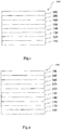
- FIG. 1 is a schematic sectional view of an organic light-emitting diode (OLED) 100, according to an exemplary embodiment of the present invention.
- the OLED 100 includes a substrate 110, an anode 120, a hole injection layer (HIL) 130, a hole transport layer (HTL) 140, an emission layer (EML) 150, an electron transport layer (ETL) 160.
- the electron transport layer (ETL) 160 is formed on the EML 150.
- an electron injection layer (EIL) 180 is disposed onto the electron transport layer (ETL) 160.
- the cathode 190 is disposed directly onto the electron injection layer (EIL) 180.
- ETL electron transport layer stack
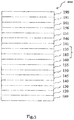
- Fig. 2 is a schematic sectional view of an OLED 100, according to another exemplary embodiment of the present invention.
- Fig. 2 differs from Fig. 1 in that the OLED 100 of Fig. 2 comprises an electron blocking layer (EBL) 145 and a hole blocking layer (HBL) 155.
- EBL electron blocking layer
- HBL hole blocking layer
- the OLED 100 includes a substrate 110, an anode 120, a hole injection layer (HIL) 130, a hole transport layer (HTL) 140, an electron blocking layer (EBL) 145, an emission layer (EML) 150, a hole blocking layer (HBL) 155, an electron transport layer (ETL) 160, an electron injection layer (EIL) 180 and a cathode electrode 190.
- HIL hole injection layer
- HTL hole transport layer
- EBL electron blocking layer
- EML emission layer
- HBL hole blocking layer
- ETL electron transport layer
- EIL electron injection layer
- the organic semiconducting layer comprising a compound (I) or consisting of a compound (I) may be an EML, an HBL or an ETL.
- Fig. 3 is a schematic sectional view of a tandem OLED 200, according to another exemplary embodiment of the present invention.
- Fig. 3 differs from Fig. 2 in that the OLED 200 of Fig. 3 further comprises a charge generation layer (CGL) and a second emission layer (151).
- CGL charge generation layer
- second emission layer 15
- the OLED 200 includes a substrate 110, an anode 120, a first hole injection layer (HIL) 130, a first hole transport layer (HTL) 140, a first electron blocking layer (EBL) 145, a first emission layer (EML) 150, a first hole blocking layer (HBL) 155, a first electron transport layer (ETL) 160, an n-type charge generation layer (n-type CGL) 185, a hole generating layer (p-type charge generation layer; p-type GCL) 135, a second hole transport layer (HTL) 141, a second electron blocking layer (EBL) 146, a second emission layer (EML) 151, a second hole blocking layer (EBL) 156, a second electron transport layer (ETL) 161, a second electron injection layer (EIL) 181 and a cathode 190.
- HIL hole injection layer
- HTL hole transport layer
- EBL electron blocking layer
- EML emission layer
- EML electron transport layer
- EML electron
- the organic semiconducting layer comprising a compound (I) or consisting of a compound (I) may be the first EML, first HBL, first ETL, n-type CGL and/or second EML, second HBL, second ETL.
- a sealing layer may further be formed on the cathode electrodes 190, in order to seal the OLEDs 100 and 200.
- various other modifications may be applied thereto.
- inventive compounds E1 to E3 were tested as electron transport material (ETM) in a model top emitting blue OLED and compared with state-of-art compound C1 as electron transport material (ETM).
- F1 is N-([1,1'biphenyl]-4-yl)-9,9-dimethyl-N-(4-(9-phenyl-9H-carbazol-3-yl)phenyl)-9H-fluoren-2-amine, CAS 1242056-42-3;
- F2 is N-(4-(dibenzo[b,d]furan-4-yl)phenyl)-N-(4-(9-phenyl-9H-fluoren-9-yl)phenyl)-[1,1'-biphenyl]-4-amine, CAS 1824678-59-2;
- F3 is 2-(3'-(9,9-dimethyl-9H-fluoren-2-yl)-[1,1'-biphenyl]-3-yl)-4,6-diphenyl-1,3,5-triazine, CAS 1955543-57-3;
- LiQ is lithium 8-hydroxyquinolinolate, H09 is a commercial blue emitter
- VTE vacuum thermal evaporation
- Metallic cathodes are prepared by VTE, in case of top-emitting devices, an additional organic light outcoupling may be provided on top of the cathode.
- the complete OLED stack may be protected from ambient conditions by suitable encapsulation, e.g. with a glass slide, and the formed cavity may comprise a getter material for moisture and/or oxygen absorption.
- the current efficiency is measured at 20°C.
- the current-voltage characteristic is determined using a Keithley 2635 source measure unit, by sourcing a voltage in V and measuring the current in mA flowing through the device under test. The voltage applied to the device is varied in steps of 0. 1V in the range between 0V and 10V.
- the luminance-voltage characteristics and CIE coordinates are determined by measuring the luminance in cd/m 2 using an Instrument Systems CAS-140CT array spectrometer (calibrated by Deutsche Ak relie für sstelle (DAkkS)) for each of the voltage values.
- the cd/A efficiency at 10 mA/cm2 is determined by interpolating the luminance-voltage and current-voltage characteristics, respectively.
- Lifetime LT of the device is measured at ambient conditions (20°C) and 30 mA/cm 2 , using a Keithley 2400 sourcemeter, and recorded in hours.
- the brightness of the device is measured using a calibrated photo diode.
- the lifetime LT is defined as the time till the brightness of the device is reduced to 97 % of its initial value.
- OLEDs are driven by constant current circuits. Those circuits can supply a constant current over a given voltage range. The wider the voltage range, the wider the power losses of such devices. Hence, the change of driving voltage upon driving needs to be minimized.
- the driving voltage of an OLED is temperature dependent. Therefore, voltage stability needs to be judged in thermal equilibrium. Thermal equilibrium is reached after one hour of driving.
- Voltage stability is measured by taking the difference of the driving voltage after 50 hours and after 1 hour driving at a constant current density.
- a current density of 30 mA/cm 2 is used. Measurements are done at room temperature.
- dU V U 50 h , 30 mA / cm 2 ⁇ U 1 h , 30 mA / cm 2
- the model device for testing the inventive compounds was a blue top emitting OLED with a structure schematically shown in Table 1.
- Table 1 Layer Material d [nm] Anode Ag 100 HIL F1:PD2 (92:8 v/v) 10 HTL F1 128 EBL F2 5 EML H09:BD200 (97:3 v/v) 20 HBL F3 5 ETL ETM:LiQ (50:50 v/v) 31 EIL Yb 2 Cathode Ag:Mg (90:10) 11
Landscapes
- Chemical & Material Sciences (AREA)
- Organic Chemistry (AREA)
- Physics & Mathematics (AREA)
- Spectroscopy & Molecular Physics (AREA)
- Engineering & Computer Science (AREA)
- Materials Engineering (AREA)
- Optics & Photonics (AREA)
- Plural Heterocyclic Compounds (AREA)
- Electroluminescent Light Sources (AREA)
- Pyridine Compounds (AREA)
Priority Applications (6)
| Application Number | Priority Date | Filing Date | Title |
|---|---|---|---|
| EP20177947.7A EP3920249A1 (fr) | 2020-06-03 | 2020-06-03 | Composé, intermédiaire du composé, procédé de préparation du composé, matériau semi-conducteur organique comprenant le composé, dispositif électronique organique comprenant le composé et dispositif d'affichage et dispositif d'éclairage comprenant le composé |
| CN202180039880.1A CN115836599A (zh) | 2020-06-03 | 2021-06-02 | 化合物、所述化合物的中间体、所述化合物的制备方法、包含所述化合物的有机半导体材料、包含所述有机半导体材料的有机电子器件以及包含所述有机电子器件的显示器件和照明器件 |
| KR1020227046159A KR20230019150A (ko) | 2020-06-03 | 2021-06-02 | 화합물, 화합물의 중간체, 화합물의 제조 방법, 화합물을 포함하는 유기 반도전 물질, 이를 포함하는 유기 전자 디바이스, 및 이를 포함하는 디스플레이 디바이스 및 조명 디바이스 |
| US18/000,597 US20230212141A1 (en) | 2020-06-03 | 2021-06-02 | Compound, Intermediate of the Compound, Process for Preparing the Compound, Organic Semiconducting Material Comprising the Compound, Organic Electronic Device Comprising the Same, and Display Device and Lighting Device Comprising the Same |
| PCT/EP2021/064813 WO2021245142A1 (fr) | 2020-06-03 | 2021-06-02 | Composé, intermédiaire du composé, procédé de préparation du composé, matériau semi-conducteur organique comprenant le composé, dispositif électronique organique le comprenant, et dispositif d'affichage et dispositif d'éclairage le comprenant |
| TW110120131A TW202200556A (zh) | 2020-06-03 | 2021-06-03 | 化合物、該化合物之中間體、該化合物製備方法、包含該化合物之有機半導體材料、包含該化合物之有機電子組件、以及包含該化合物之顯示裝置與照明裝置 |
Applications Claiming Priority (1)
| Application Number | Priority Date | Filing Date | Title |
|---|---|---|---|
| EP20177947.7A EP3920249A1 (fr) | 2020-06-03 | 2020-06-03 | Composé, intermédiaire du composé, procédé de préparation du composé, matériau semi-conducteur organique comprenant le composé, dispositif électronique organique comprenant le composé et dispositif d'affichage et dispositif d'éclairage comprenant le composé |
Publications (1)
| Publication Number | Publication Date |
|---|---|
| EP3920249A1 true EP3920249A1 (fr) | 2021-12-08 |
Family
ID=70977378
Family Applications (1)
| Application Number | Title | Priority Date | Filing Date |
|---|---|---|---|
| EP20177947.7A Pending EP3920249A1 (fr) | 2020-06-03 | 2020-06-03 | Composé, intermédiaire du composé, procédé de préparation du composé, matériau semi-conducteur organique comprenant le composé, dispositif électronique organique comprenant le composé et dispositif d'affichage et dispositif d'éclairage comprenant le composé |
Country Status (6)
| Country | Link |
|---|---|
| US (1) | US20230212141A1 (fr) |
| EP (1) | EP3920249A1 (fr) |
| KR (1) | KR20230019150A (fr) |
| CN (1) | CN115836599A (fr) |
| TW (1) | TW202200556A (fr) |
| WO (1) | WO2021245142A1 (fr) |
Citations (9)
| Publication number | Priority date | Publication date | Assignee | Title |
|---|---|---|---|---|
| EP1970371A1 (fr) | 2007-03-16 | 2008-09-17 | Novaled AG | Pyrido(3,2-h)chinazoline et/ou leurs dérivés 5,6-dihydro, leur procédé de fabrication et matériau semi-conducteur organique en étant doté |
| WO2013079217A1 (fr) | 2011-11-30 | 2013-06-06 | Novaled Ag | Afficheur |
| EP2722908A1 (fr) | 2012-10-17 | 2014-04-23 | Novaled AG | Diode électroluminescente organique phosphorescente et matières de transport de trous pour diodes électroluminescentes phosphorescentes |
| EP3312896A1 (fr) | 2016-10-24 | 2018-04-25 | Novaled GmbH | Dispositif électroluminescent organique comprenant une couche de transport d'électrons dopés redox et une couche auxiliaire de transport d'électrons |
| EP3312895A1 (fr) | 2016-10-24 | 2018-04-25 | Novaled GmbH | Matériau organique semi-conducteur comprenant un dopant-n électrique et une matrice de transport d'électrons et dispositif électronique comprenant le matériau semi-conducteur |
| EP3312899A1 (fr) | 2016-10-24 | 2018-04-25 | Novaled GmbH | Empilement de couches de transport d'électrons pour une diode électroluminescente organique |
| WO2018077689A1 (fr) | 2016-10-24 | 2018-05-03 | Novaled Gmbh | Composé pour dispositif électronique, dispositif électronique et dispositif d'affichage |
| EP3502106A1 (fr) * | 2017-12-21 | 2019-06-26 | Novaled GmbH | Composés de triazine substitués par des groupes volumineux |
| CN110105244A (zh) * | 2019-05-14 | 2019-08-09 | 华南理工大学 | 一种含四苯基苯的有机发光材料及制备与应用 |
Family Cites Families (3)
| Publication number | Priority date | Publication date | Assignee | Title |
|---|---|---|---|---|
| CN102482279B (zh) * | 2009-03-30 | 2015-08-12 | 德山新勒克斯 | 有机电子装置及其化合物与终端机 |
| EP3171418B1 (fr) * | 2015-11-23 | 2024-12-11 | Novaled GmbH | Couche semi-conductrice organique comprenant des composés d'oxyde de phosphine |
| EP3653619A1 (fr) * | 2018-11-16 | 2020-05-20 | Novaled GmbH | Composé, dispositif électronique organique le comprenant, dispositif d'affichage et dispositif d'éclairage le comprenant |
-
2020
- 2020-06-03 EP EP20177947.7A patent/EP3920249A1/fr active Pending
-
2021
- 2021-06-02 KR KR1020227046159A patent/KR20230019150A/ko active Pending
- 2021-06-02 US US18/000,597 patent/US20230212141A1/en active Pending
- 2021-06-02 CN CN202180039880.1A patent/CN115836599A/zh active Pending
- 2021-06-02 WO PCT/EP2021/064813 patent/WO2021245142A1/fr not_active Ceased
- 2021-06-03 TW TW110120131A patent/TW202200556A/zh unknown
Patent Citations (10)
| Publication number | Priority date | Publication date | Assignee | Title |
|---|---|---|---|---|
| EP1970371A1 (fr) | 2007-03-16 | 2008-09-17 | Novaled AG | Pyrido(3,2-h)chinazoline et/ou leurs dérivés 5,6-dihydro, leur procédé de fabrication et matériau semi-conducteur organique en étant doté |
| WO2013079217A1 (fr) | 2011-11-30 | 2013-06-06 | Novaled Ag | Afficheur |
| EP2722908A1 (fr) | 2012-10-17 | 2014-04-23 | Novaled AG | Diode électroluminescente organique phosphorescente et matières de transport de trous pour diodes électroluminescentes phosphorescentes |
| EP3312896A1 (fr) | 2016-10-24 | 2018-04-25 | Novaled GmbH | Dispositif électroluminescent organique comprenant une couche de transport d'électrons dopés redox et une couche auxiliaire de transport d'électrons |
| EP3312895A1 (fr) | 2016-10-24 | 2018-04-25 | Novaled GmbH | Matériau organique semi-conducteur comprenant un dopant-n électrique et une matrice de transport d'électrons et dispositif électronique comprenant le matériau semi-conducteur |
| EP3312899A1 (fr) | 2016-10-24 | 2018-04-25 | Novaled GmbH | Empilement de couches de transport d'électrons pour une diode électroluminescente organique |
| WO2018077689A1 (fr) | 2016-10-24 | 2018-05-03 | Novaled Gmbh | Composé pour dispositif électronique, dispositif électronique et dispositif d'affichage |
| EP3502106A1 (fr) * | 2017-12-21 | 2019-06-26 | Novaled GmbH | Composés de triazine substitués par des groupes volumineux |
| WO2019121672A1 (fr) | 2017-12-21 | 2019-06-27 | Novaled Gmbh | Composés de triazine substitués par des groupes volumineux |
| CN110105244A (zh) * | 2019-05-14 | 2019-08-09 | 华南理工大学 | 一种含四苯基苯的有机发光材料及制备与应用 |
Non-Patent Citations (3)
| Title |
|---|
| CHEMICAL ABSTRACTS, Columbus, Ohio, US; abstract no. 12 6-42-3 |
| PENGBO HAN ET AL: "Tetraphenylbenzene-based AIEgens: horizontally oriented emitters for highly efficient non-doped deep blue OLEDs and hosts for high-performance hybrid WOLEDs", JOURNAL OF MATERIALS CHEMISTRY C, vol. 8, no. 21, 7 April 2020 (2020-04-07), GB, pages 7012 - 7018, XP055744335, ISSN: 2050-7526, DOI: 10.1039/D0TC00920B * |
| YASUHIKO SHIROTAHIROSHI KAGEYAMA, CHEM. REV., vol. 107, 2007, pages 953 - 1010 |
Also Published As
| Publication number | Publication date |
|---|---|
| TW202200556A (zh) | 2022-01-01 |
| WO2021245142A1 (fr) | 2021-12-09 |
| CN115836599A (zh) | 2023-03-21 |
| KR20230019150A (ko) | 2023-02-07 |
| US20230212141A1 (en) | 2023-07-06 |
Similar Documents
| Publication | Publication Date | Title |
|---|---|---|
| EP3895227B1 (fr) | Dispositif électroluminescent organique et composition solide destinée à être utilisée dans ce dernier | |
| EP3895226B1 (fr) | Dispositif électroluminescent organique et composé à utiliser en son sein | |
| KR102864604B1 (ko) | 스피로 벤조안트라센-플루오렌 유도체 및 유기 전자 디바이스, 디스플레이 및 발광 디바이스에서 이들의 용도 | |
| EP3670504A1 (fr) | Composé et couche semiconductrice organique, dispositif électronique organique et dispositif d'affichage le comprenant | |
| KR102794334B1 (ko) | 유기 전자 디바이스, 이를 포함하는 디스플레이 및 조명 디바이스 | |
| KR102634897B1 (ko) | 트리아진 화합물 및 이를 포함하는 유기 반도전층 | |
| EP3556746A1 (fr) | Composé, son procédé de préparation, couche semiconductrice organique, dispositif électronique organique, affichage et dispositif d'éclairage le comprenant | |
| WO2021122155A1 (fr) | Dispositif électronique organique et dispositif d'affichage comprenant le dispositif électronique organique | |
| JP2022551459A (ja) | 化合物、並びに有機半導体層、有機電子デバイス、表示デバイス及びそれを含む照明デバイス | |
| WO2023117255A1 (fr) | Diode électroluminescente organique, dispositif d'affichage la comprenant et composé | |
| EP3930024B1 (fr) | Dispositif électronique organique et dispositif d'affichage comprenant le dispositif électronique organique ainsi qu'une composition destinée à être utilisée dans des dispositifs électroniques organiques | |
| EP4106028A1 (fr) | Dispositif électronique organique comprenant un composé de formule (i), dispositif d'affichage comprenant le dispositif électronique organique, ainsi que composés de formule (i) | |
| EP3693352A1 (fr) | Composé et couche semiconductrice organique, dispositif électronique organique et dispositif d'affichage ou d'éclairage le comprenant | |
| EP3920249A1 (fr) | Composé, intermédiaire du composé, procédé de préparation du composé, matériau semi-conducteur organique comprenant le composé, dispositif électronique organique comprenant le composé et dispositif d'affichage et dispositif d'éclairage comprenant le composé | |
| EP4572585A1 (fr) | Composé et diode électroluminescente organique | |
| EP4346356A1 (fr) | Matériau semi-conducteur, procédé de préparation d'une couche du matériau semi-conducteur, dispositif semi-conducteur organique comprenant le matériau semi-conducteur et composé | |
| EP4472385A1 (fr) | Dispositif électroluminescent organique et dispositif d'affichage le comprenant | |
| US12382829B2 (en) | Compound and an organic semiconducting layer, an organic electronic device and a display or lighting device comprising the same | |
| EP3696179B1 (fr) | Composé et couche semiconductrice organique, dispositif électronique organique et dispositif d'affichage ou d'éclairage le comprenant | |
| EP3726599A1 (fr) | Composé, matériau semiconducteur organique le comprenant, dispositif électronique organique le comprenant, dispositif d'affichage et dispositif d'éclairage le comprenant | |
| CN118434721A (zh) | 用于适合电子器件的半导体材料中的化合物 |
Legal Events
| Date | Code | Title | Description |
|---|---|---|---|
| PUAI | Public reference made under article 153(3) epc to a published international application that has entered the european phase |
Free format text: ORIGINAL CODE: 0009012 |
|
| STAA | Information on the status of an ep patent application or granted ep patent |
Free format text: STATUS: THE APPLICATION HAS BEEN PUBLISHED |
|
| AK | Designated contracting states |
Kind code of ref document: A1 Designated state(s): AL AT BE BG CH CY CZ DE DK EE ES FI FR GB GR HR HU IE IS IT LI LT LU LV MC MK MT NL NO PL PT RO RS SE SI SK SM TR |
|
| B565 | Issuance of search results under rule 164(2) epc |
Effective date: 20201112 |
|
| STAA | Information on the status of an ep patent application or granted ep patent |
Free format text: STATUS: REQUEST FOR EXAMINATION WAS MADE |
|
| 17P | Request for examination filed |
Effective date: 20220601 |
|
| RBV | Designated contracting states (corrected) |
Designated state(s): AL AT BE BG CH CY CZ DE DK EE ES FI FR GB GR HR HU IE IS IT LI LT LU LV MC MK MT NL NO PL PT RO RS SE SI SK SM TR |
|
| STAA | Information on the status of an ep patent application or granted ep patent |
Free format text: STATUS: EXAMINATION IS IN PROGRESS |
|
| 17Q | First examination report despatched |
Effective date: 20231124 |