EP3919876A1 - Optical module, signal processing system, and signal processing method - Google Patents
Optical module, signal processing system, and signal processing method Download PDFInfo
- Publication number
- EP3919876A1 EP3919876A1 EP20749527.6A EP20749527A EP3919876A1 EP 3919876 A1 EP3919876 A1 EP 3919876A1 EP 20749527 A EP20749527 A EP 20749527A EP 3919876 A1 EP3919876 A1 EP 3919876A1
- Authority
- EP
- European Patent Office
- Prior art keywords
- intensity
- mirror
- light
- acquiring
- laser light
- Prior art date
- Legal status (The legal status is an assumption and is not a legal conclusion. Google has not performed a legal analysis and makes no representation as to the accuracy of the status listed.)
- Granted
Links
Images












Classifications
-
- G—PHYSICS
- G01—MEASURING; TESTING
- G01J—MEASUREMENT OF INTENSITY, VELOCITY, SPECTRAL CONTENT, POLARISATION, PHASE OR PULSE CHARACTERISTICS OF INFRARED, VISIBLE OR ULTRAVIOLET LIGHT; COLORIMETRY; RADIATION PYROMETRY
- G01J3/00—Spectrometry; Spectrophotometry; Monochromators; Measuring colours
- G01J3/28—Investigating the spectrum
- G01J3/45—Interferometric spectrometry
- G01J3/453—Interferometric spectrometry by correlation of the amplitudes
- G01J3/4535—Devices with moving mirror
-
- G—PHYSICS
- G01—MEASURING; TESTING
- G01B—MEASURING LENGTH, THICKNESS OR SIMILAR LINEAR DIMENSIONS; MEASURING ANGLES; MEASURING AREAS; MEASURING IRREGULARITIES OF SURFACES OR CONTOURS
- G01B9/00—Measuring instruments characterised by the use of optical techniques
- G01B9/02—Interferometers
- G01B9/02015—Interferometers characterised by the beam path configuration
-
- G—PHYSICS
- G01—MEASURING; TESTING
- G01J—MEASUREMENT OF INTENSITY, VELOCITY, SPECTRAL CONTENT, POLARISATION, PHASE OR PULSE CHARACTERISTICS OF INFRARED, VISIBLE OR ULTRAVIOLET LIGHT; COLORIMETRY; RADIATION PYROMETRY
- G01J3/00—Spectrometry; Spectrophotometry; Monochromators; Measuring colours
- G01J3/02—Details
- G01J3/027—Control of working procedures of a spectrometer; Failure detection; Bandwidth calculation
-
- G—PHYSICS
- G01—MEASURING; TESTING
- G01J—MEASUREMENT OF INTENSITY, VELOCITY, SPECTRAL CONTENT, POLARISATION, PHASE OR PULSE CHARACTERISTICS OF INFRARED, VISIBLE OR ULTRAVIOLET LIGHT; COLORIMETRY; RADIATION PYROMETRY
- G01J3/00—Spectrometry; Spectrophotometry; Monochromators; Measuring colours
- G01J3/28—Investigating the spectrum
-
- G—PHYSICS
- G01—MEASURING; TESTING
- G01J—MEASUREMENT OF INTENSITY, VELOCITY, SPECTRAL CONTENT, POLARISATION, PHASE OR PULSE CHARACTERISTICS OF INFRARED, VISIBLE OR ULTRAVIOLET LIGHT; COLORIMETRY; RADIATION PYROMETRY
- G01J3/00—Spectrometry; Spectrophotometry; Monochromators; Measuring colours
- G01J3/28—Investigating the spectrum
- G01J3/45—Interferometric spectrometry
-
- G—PHYSICS
- G02—OPTICS
- G02B—OPTICAL ELEMENTS, SYSTEMS OR APPARATUS
- G02B26/00—Optical devices or arrangements for the control of light using movable or deformable optical elements
- G02B26/06—Optical devices or arrangements for the control of light using movable or deformable optical elements for controlling the phase of light
-
- G—PHYSICS
- G02—OPTICS
- G02B—OPTICAL ELEMENTS, SYSTEMS OR APPARATUS
- G02B26/00—Optical devices or arrangements for the control of light using movable or deformable optical elements
- G02B26/08—Optical devices or arrangements for the control of light using movable or deformable optical elements for controlling the direction of light
- G02B26/0816—Optical devices or arrangements for the control of light using movable or deformable optical elements for controlling the direction of light by means of one or more reflecting elements
- G02B26/0833—Optical devices or arrangements for the control of light using movable or deformable optical elements for controlling the direction of light by means of one or more reflecting elements the reflecting element being a micromechanical device, e.g. a MEMS mirror, DMD
- G02B26/0841—Optical devices or arrangements for the control of light using movable or deformable optical elements for controlling the direction of light by means of one or more reflecting elements the reflecting element being a micromechanical device, e.g. a MEMS mirror, DMD the reflecting element being moved or deformed by electrostatic means
-
- G—PHYSICS
- G01—MEASURING; TESTING
- G01J—MEASUREMENT OF INTENSITY, VELOCITY, SPECTRAL CONTENT, POLARISATION, PHASE OR PULSE CHARACTERISTICS OF INFRARED, VISIBLE OR ULTRAVIOLET LIGHT; COLORIMETRY; RADIATION PYROMETRY
- G01J3/00—Spectrometry; Spectrophotometry; Monochromators; Measuring colours
- G01J3/02—Details
- G01J3/0205—Optical elements not provided otherwise, e.g. optical manifolds, diffusers, windows
- G01J3/021—Optical elements not provided otherwise, e.g. optical manifolds, diffusers, windows using plane or convex mirrors, parallel phase plates, or particular reflectors
-
- G—PHYSICS
- G01—MEASURING; TESTING
- G01J—MEASUREMENT OF INTENSITY, VELOCITY, SPECTRAL CONTENT, POLARISATION, PHASE OR PULSE CHARACTERISTICS OF INFRARED, VISIBLE OR ULTRAVIOLET LIGHT; COLORIMETRY; RADIATION PYROMETRY
- G01J3/00—Spectrometry; Spectrophotometry; Monochromators; Measuring colours
- G01J3/02—Details
- G01J3/0256—Compact construction
-
- G—PHYSICS
- G01—MEASURING; TESTING
- G01J—MEASUREMENT OF INTENSITY, VELOCITY, SPECTRAL CONTENT, POLARISATION, PHASE OR PULSE CHARACTERISTICS OF INFRARED, VISIBLE OR ULTRAVIOLET LIGHT; COLORIMETRY; RADIATION PYROMETRY
- G01J3/00—Spectrometry; Spectrophotometry; Monochromators; Measuring colours
- G01J3/02—Details
- G01J3/06—Scanning arrangements arrangements for order-selection
Definitions
- the storage unit may further include a third storage region, and the third storage region may be a region that stores each of the first measurement light intensity and the first laser light intensity acquired in the latest one cycle among the P cycles (P is an integer of four or greater) until transmitting the first measurement light intensity and the first laser light intensity to the first storage region in a case where the first intensity acquisition process is performed, and stores each of the second measurement light intensity and the second laser light intensity acquired in the latest one cycle among the P cycles (P is an integer of four or greater) until transmitting the second measurement light intensity and the second laser light intensity to the second storage region in a case where the second intensity acquisition process is performed.
- P is an integer of four or greater
- a signal processing system includes: an optical module; and a signal processing device that is electrically connected to the optical module.
- the optical module includes a mirror device that includes a base, a movable mirror including a mirror surface, an elastic support portion that is connected between the base and the movable mirror and supports the movable mirror so that the movable mirror is movable along a direction intersecting the mirror surface, a first comb electrode that is provided in the base and includes a plurality of first comb fingers, and a second comb electrode that is provided in at least one of the movable mirror and the elastic support portion and includes a plurality of second comb fingers arranged alternately with the plurality of first comb fingers, at least one fixed mirror, at least one beam splitter that constitutes an interference optical system in combination with the movable mirror and the at least one fixed mirror, a first light detector that detects interference light of measurement light emitted from the interference optical system, a second light detector that detects interference light of laser light emitted from the interference optical
- the outer beam portion 224b is disposed on a surface of the frame portion 222 on the one side in the Z-axis direction.
- the outer beam portion 224b surrounds the inner beam portion 224a and the mirror surface 22a when viewed from the Z-axis direction.
- an outer edge of the outer beam portion 224b extends along an outer edge of the frame portion 222 with a predetermined gap from the outer edge of the frame portion 222 when viewed from the Z-axis direction.
- An inner edge of the outer beam portion 224b extends along an inner edge of the frame portion 222 with a predetermined gap from the inner edge of the frame portion 222 when viewed from the Z-axis direction.
- An end surface 224bs of the outer beam portion 224b on the one side in the Z-axis direction is located on the one side in the Z-axis direction in comparison to the mirror surface 22a.
- the support layer 101 that constitutes the inner beam portion 224a, the outer beam portion 224b, and the respective connection beam portions 224c is thinner than the support layer 101 that constitutes the base 21. Accordingly, the end surfaces 224as, 224bs, and 224cs are located on the one side in the Z-axis direction in comparison to the first surface 21a of the base 21. In other words, the first surface 21a is located on the other side in the Z-axis direction in comparison to the end surfaces 224as, 224bs, and 224cs.
- a length of the first portion 261a in the X-axis direction is shorter than a length of the second portion 261b in the X-axis direction.
- the third portions 261c of the pair of levers 261 obliquely extend to be spaced away from each other as going away from the movable mirror 22.
- the pair of beam members 264 respectively bridge the second portions 261b of the pair of levers 261 and the first link member 262.
- the respective beam members 264 have a plate shape that extends along a plane perpendicular to the Z-axis direction.
- the pair of beam members 264 obliquely extend to approach each other as going away from the movable mirror 22.
- the pair of levers 261, the first link member 262, the second link member 263, and the pair of beam members 264 define the light passage portion 24.
- the light passage portion 24 has a polygonal shape when viewed from the Z-axis direction.
- the light passage portion 24 is a cavity (hole).
- a material having optical transparency with respect to the measurement light L0 and the laser light L10 may be disposed in the light passage portion 24.
- the pair of second electrode support portions 269b are disposed on the same central line parallel to the Y-axis direction.
- the pair of third electrode support portions 269c are disposed on the same central line parallel to the Y-axis direction. In the X-axis direction, the first electrode support portions 269a, the second electrode support portions 269b, and the third electrode support portions 269c are aligned in this order from the movable mirror 22 side.
- the intermediate member 275 has a plate shape that extends along a plane perpendicular to the Z-axis direction, and extends in the Y-axis direction.
- the intermediate member 275 is disposed between the movable mirror 22 and the second link member 273 (in other words, between the movable mirror 22 and the light passage portion 25).
- the intermediate member 275 is connected to the movable mirror 22 through the non-linearity mitigation springs 278 as to be described later.
- the base 21 of the mirror device 20 is provided with a sixth surface 21d that is spaced apart from the optical function member 13 in a state in which the third surface 13a of the optical function member 13 and the second surface 21b of the base 21 are joined to each other.
- the sixth surface 21d is spaced apart from the optical function member 13 in a region including at least a part of the outer edge of the base 21 when viewed from the Z-axis direction.
- the sixth surface 21d is formed by etching and removing the device layer 102 and the intermediate layer 103 along one side extending in the Y-axis direction in the outer edge of the base 21.
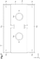
- a plurality of reference holes 13e are formed in the third surface 13a of the optical function member 13.
- the second light detector 8 is disposed in the second through-hole 136.
- the second light detector 8 includes a light detection element 82, and a package 84 including a condensing lens 84a.
- the light detection element 82 detects interference light L11 of the laser light.
- the light detection element 82 is a Si photodiode.
- the condensing lens 84a condenses the interference light L11 of the laser light which is incident to the light detection element 82 to the light detection element 82.
- An optical axis of the light detection element 82 and an optical axis of the condensing lens 84a match each other.
- the first mirror 51 is a dichroic mirror that has a function of allowing the measurement light L0 to be transmitted therethrough and reflecting the laser light L10, and is inclined with respect to an optical axis of the first light detector 6.
- the first mirror 51 is disposed between the beam splitter unit 3 and the first light detector 6. That is, the first mirror 51 is disposed to face the beam splitter unit 3 and the first light detector 6.
- an optical surface of the first mirror 51 is a surface that is parallel to the Y-axis direction and has an angle of 45° with respect to the Z-axis direction. Note that, an optical axis of the first light detector 6 is parallel to the Z-axis direction.
- a laser light absorption unit 57 is disposed on a side opposite to the second light detector 8 with respect to the second mirror 52.
- the laser light absorption unit 57 has a function of absorbing the laser light L10.
- the laser light absorption unit 57 is a part of the second support structure (support) 12 that supports the second mirror 52. More specifically, the laser light absorption unit 57 is a portion that protrudes from the side wall portion 125 of the main body portion 121 of the connection unit 120 to the beam splitter unit 3 side.
- the laser light absorption unit 57 is constituted by forming a black resist layer on the portion, or by performing a black alumite treatment to the portion.
- the laser light absorption unit 57 is a part of the second support structure 12, and thus an increase in the number of parts is suppressed.
- a distance from an intersection between the optical path and the first mirror surface 31 of the beam splitter unit 3 to a light incident surface of the first light detector 6 is shorter than a distance from an intersection between an optical path and the first mirror surface 31 of the beam splitter unit 3 to a light incident surface of the second light detector 8, and is shorter than a distance from an intersection between an optical path and the first mirror surface 31 of the beam splitter unit 3 to a light emission surface of the second light source 7.
- a distance from the optical surface 33a of the beam splitter unit 3 to the light incident surface of the first light detector 6 is shorter than a distance from the optical surface 33a of the beam splitter unit 3 to the light incident surface of the second light detector 8, and is shorter than a distance from the optical surface 33a of the beam splitter unit 3 to the light emission surface of the second light source 7.
- the timings correspond to a timing at which a maximum value M1 (for example, a position farthest from the beam splitter unit 3) appears and a timing at which a minimum value M2 (for example, a position closest to the beam splitter unit 3) appears in the temporal variation of the position of the movable mirror 22, and thus the timings at which the maximum value M1 and the minimum value M2 appear may be detected.
- a maximum value M1 for example, a position farthest from the beam splitter unit 3
- a minimum value M2 for example, a position closest to the beam splitter unit
- a center burst (CB) in the temporal variation of the intensity of the interference light L1 of the measurement light appears in the first half of the period T1 and the second half of the period T2.
- CB center burst
- a rising timing of the voltage signal matches the timings at which the maximum value M1 and the minimum value M2 appear as return positions of the movable mirror 22.
- a solid-line arrow represents a movement direction of the movable mirror 22
- a broken-line arrow represents a direction of a force that occurs in the movable mirror 22.
- a hatched fixed comb electrode 281 (283) represents a state in which a voltage is applied
- a non-hatched fixed comb electrode 281 (283) represents a state in which a voltage is not applied.
- the intensity acquisition unit 202 (refer to FIG. 11 ) performs a first intensity acquisition process and a second intensity acquisition process.
- first intensity acquisition process and the second intensity acquisition process will be described in detail.
- the intensity data in a case where the LSB logic is "0" corresponds to the intensity data in the period T1
- the intensity data in a case where the LSB logic is "1” corresponds to the intensity data in the period T2.
- the signal processing unit 200 counts the number of cycles of the voltage logic and generates the LSB logic by using one bit.
- the plurality of first measurement light intensities mutually corresponding for the same number of times represent a plurality of the first measurement light intensities acquired for the same number of times through counting from the rising of the voltage signal in each of the odd-numbered cycles
- the plurality of first laser light intensities mutually corresponding for the same number of times represent a plurality of the first laser light intensities acquired for the same number of times through counting from the rising of the voltage signal in each of the odd-numbered cycles.
- the plurality of second measurement light intensities mutually corresponding for the same number of times represent a plurality of the second measurement light intensities acquired for the same number of times through counting from the rising of the voltage signal in each of the even-numbered cycles
- the plurality of second laser light intensities mutually corresponding for the same number of times represent a plurality of the second laser light intensities acquired for the same number of times through counting from the rising of the voltage signal in each of the even-numbered cycles.
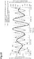
- the intensity acquisition unit 202 performs the second intensity acquisition process, as illustrated in FIG. 23 , with respect to even-numbered cycles (cycles in which the LSB logic is shown as "0", and which correspond to the period T1), a temporal variation of an average value of the first measurement light intensity and a temporal variation of an average value of the first laser light intensity are acquired.
- the intensity acquisition unit 202 performs the first intensity acquisition process, as illustrated in FIG. 24 , with respect to odd-numbered cycles (cycles in which the LSB logic is shown as "1", and which correspond to the period T2), a temporal variation of an average value of the second measurement light intensity and a temporal variation of an average value of the second laser light intensity are acquired.
- the second intensity value at a timing at which the maximum value or the minimum value appears in the temporal variation of the average value of the second laser light intensity may be acquired from the temporal variation of the average value of the second measurement light intensity, the relationship between the optical path difference and the second intensity value may be acquired on the basis of the wavelength of the laser light L10, and the spectrum of the measurement light L0 may be acquired by the Fourier transformation.
- the first intensity value at a timing at which an intermediate value (an intermediate value between the maximum value and the minimum value which are continuous) appears in the temporal variation of the average value of the first laser light intensity may be acquired, and the first intensity value may be used in acquisition of the spectrum of the measurement light L0.
- the second intensity value at a timing at which an intermediate value (an intermediate value between the maximum value and the minimum value which are continuous) appears in the temporal variation of the average value of the second laser light intensity may be acquired, and the second intensity value may be used in acquisition of the spectrum of the measurement light L0.
- the intensity of the interference light L1 of the measurement light and the intensity of the interference light L11 of the laser light can be acquired at a desired timing while causing the movable mirror 22 to resonate continuously.
- a period (that is, a numerical value of P in the P cycles) of acquiring the intensity of the interference light L1 of the measurement light and the intensity of the interference light L11 of the laser light can be set, for example, in the PC 500.
- the holding unit 130 holds the first light source 5, the second light source 7, and the second light detector 8 so that the first light source 5, the second light source 7, and the second light detector 8 face one side in the Z-axis direction on one side of the mirror unit 2 in the X-axis direction, and are aligned in the order of the first light source 5, the second light source 7, and the second light detector 8 from the other side (that is, the mirror unit 2 side) in the X-axis direction.
- the first light source 5 includes a light-emitting element 5a and a condensing lens 5b.
- the light-emitting element 5a is a thermal type light source such as a filament.
- the condensing lens 5b condenses the measurement light L0.
Landscapes
- Physics & Mathematics (AREA)
- Spectroscopy & Molecular Physics (AREA)
- General Physics & Mathematics (AREA)
- Optics & Photonics (AREA)
- Spectrometry And Color Measurement (AREA)
- Mechanical Light Control Or Optical Switches (AREA)
Abstract
Description
- The present disclosure relates to an optical module, a signal processing system, and a signal processing method.
- As a signal processing method for Fourier transformation type spectral analysis,
Patent Literature 1 discloses a method in which a plurality of pieces of measurement data are acquired from a signal representing the intensity of interference light of light to be measured which is generated by an interference system at timing at which a signal representing the intensity of interference light of monochromatic light generated by the interference system intersects a reference voltage, and a plurality of interferograms in accordance with the plurality of pieces of measurement data are integrated while performing alignment at a center burst position. - Patent Literature 1:
Japanese Unexamined Patent Publication No. 2013-250127 - In the signal processing method described in
Patent Literature 1, since it is necessary to perform the alignment at the center burst position to integrate the plurality of interferograms, it is difficult to perform Fourier transformation type spectral analysis in a short time. - An object of the present disclosure is to provide an optical module, a signal processing system, and a signal processing method which enable Fourier transformation type spectral analysis to be performed in a short time.
- An optical module according to an aspect of the present disclosure includes: a mirror device that includes a base, a movable mirror including a mirror surface, an elastic support portion that is connected between the base and the movable mirror and supports the movable mirror so that the movable mirror is movable along a direction intersecting the mirror surface, a first comb electrode that is provided in the base and includes a plurality of first comb fingers, and a second comb electrode that is provided in at least one of the movable mirror and the elastic support portion and includes a plurality of second comb fingers arranged alternately with the plurality of first comb fingers; at least one fixed mirror; at least one beam splitter that constitutes an interference optical system in combination with the movable mirror and the at least one fixed mirror; a first light detector that detects interference light of measurement light emitted from the interference optical system; a second light detector that detects interference light of laser light emitted from the interference optical system; and a signal processing unit that is electrically connected to each of the mirror device, the first light detector, and the second light detector. The signal processing unit includes a voltage signal control unit that controls a voltage signal having a frequency for causing the movable mirror to resonate in the mirror device, so that the voltage signal is applied between the first comb electrode and the second comb electrode, and an intensity acquisition unit that performs an intensity acquisition process of acquiring a measurement light intensity of the interference light of the measurement light M times (M is an integer of two or greater) at a first time interval based on the frequency in each of a plurality of cycles among P cycles (P is an integer of two or greater) continuous in the voltage signal, acquiring an addition value of a plurality of the measurement light intensities mutually corresponding for the same number of times, acquiring a laser light intensity of the interference light of the laser light N times (N is an integer of two or greater) at a second time interval based on the frequency in each of the plurality of cycles, and acquiring an addition value of a plurality of the laser light intensities mutually corresponding for the same number of times.
- In the optical module, a voltage signal is controlled so that a voltage signal having a frequency for causing the movable mirror to resonate in the mirror device is applied between the first comb electrode and the second comb electrode. The frequency of the voltage signal ideally becomes a value two times a resonance frequency of the movable mirror. Accordingly, when acquiring the measurement light intensity of the interference light of the measurement light M times at the first time interval based on the frequency of the voltage signal in each of a plurality of cycles among P cycles continuous in the voltage signal, and acquiring the addition value of the plurality of measurement light intensities mutually corresponding for the same number of times, the addition value of the measurement light intensities can be easily and accurately acquired for every same position in a case where the movable mirror moves. Similarly, when acquiring the laser light intensity of the interference light of the laser light N times at the second time interval based on the frequency of the voltage signal in each of the plurality of cycles, and acquiring the addition value of the plurality of laser light intensities mutually corresponding for the same number of times, the addition value of the laser light intensities can be easily and accurately acquired for every same position in a case where the movable mirror moves. Accordingly, the optical module enables Fourier transformation type spectral analysis to be performed in a short time.
- In the optical module according to the aspect of the present disclosure, the intensity acquisition unit may perform at least one of a first intensity acquisition process and a second intensity acquisition process as the intensity acquisition process, the first intensity acquisition process may be a process of acquiring a first measurement light intensity the M times at the first time interval in each of odd-numbered cycles among P cycles (P is an integer of four or greater) continuous in the voltage signal as the measurement light intensity, acquiring an addition value of a plurality of the first measurement light intensities mutually corresponding for the same number of times, acquiring a first laser light intensity the N times at the second time interval in each of the odd-numbered cycles as the laser light intensity, and acquiring an addition value of a plurality of the first laser light intensities mutually corresponding for the same number of times, and the second intensity acquisition process may be a process of acquiring a second measurement light intensity the M times at the first time interval in each of even-numbered cycles among the P cycles (P is an integer of four or greater) as the measurement light intensity, acquiring an addition value of a plurality of the second measurement light intensities mutually corresponding for the same number of times, acquiring a second laser light intensity the N times at the second time interval in each of the even-numbered cycles as the laser light intensity, and acquiring an addition value of a plurality of the second laser light intensities mutually corresponding for the same number of times. According to this, when acquiring the first measurement light intensity M times at the first time interval in each of odd-numbered cycles among P cycles continuous in the voltage signal as the measurement light intensity, and acquiring the addition value of the plurality of first measurement light intensities mutually corresponding for the same number of times, the addition value of the first measurement light intensities can be easily and accurately acquired for every same position in a case where the movable mirror moves in one direction of reciprocation directions. Similarly, when acquiring the first laser light intensity N times at the second time interval in each of the odd-numbered cycles as the laser light intensity, and acquiring the addition value of the plurality of first laser light intensities mutually corresponding for the same number of times, the addition value of the first laser light intensities can be easily and accurately acquired for every same position in a case where the movable mirror moves in the one direction of the reciprocation directions. In addition, when acquiring the second measurement light intensity M times at the first time interval in each of even-numbered cycles among the P cycles continuous in the voltage signal as the measurement light intensity, and acquiring an addition value of a plurality of the second measurement light intensities mutually corresponding for the same number of times, the addition value of the second measurement light intensities can be easily and accurately acquired for every same position in a case where the movable mirror moves in the other direction of the reciprocation directions. Similarly, when acquiring the second laser light intensity N times at the second time interval in each of the even-numbered cycles as the laser light intensity, and acquiring the addition value of the plurality of second laser light intensities mutually corresponding for the same number of times, the addition value of the second laser light intensities can be easily and accurately acquired for every same position in a case where the movable mirror moves in the other direction of the reciprocation directions. Accordingly, the optical module enables more accurate Fourier transformation type spectral analysis to be performed in a short time.
- The optical module according to the aspect of the present disclosure may further include a storage unit that includes at least one of a first storage region and a second storage region. The first storage region may be a region that stores values obtained by integrating or averaging each of the first measurement light intensity and the first laser light intensity acquired in each of the odd-numbered cycles for every one cycle in a case where the first intensity acquisition process is performed, and the second storage region may be a region that stores values obtained by integrating or averaging each of the second measurement light intensity and the second laser light intensity acquired in each of the even-numbered cycles for every one cycle in a case where the second intensity acquisition process is performed. According to this, the first intensity acquisition process and the second intensity acquisition process can be reliably performed while suppressing storage capacity of the storage unit.
- In the optical module according to the aspect of the present disclosure, the storage unit may further include a third storage region, and the third storage region may be a region that stores each of the first measurement light intensity and the first laser light intensity acquired in the latest one cycle among the P cycles (P is an integer of four or greater) until transmitting the first measurement light intensity and the first laser light intensity to the first storage region in a case where the first intensity acquisition process is performed, and stores each of the second measurement light intensity and the second laser light intensity acquired in the latest one cycle among the P cycles (P is an integer of four or greater) until transmitting the second measurement light intensity and the second laser light intensity to the second storage region in a case where the second intensity acquisition process is performed. According to this, it is possible to confirm whether or not each piece of intensity data is correct during temporarily storing each piece of intensity data in the third storage region.
- In the optical module according to the aspect of the present disclosure, a zero optical path difference position of the movable mirror, at which an optical path length on the movable mirror side with which the interference light of the measurement light is caused to occur becomes the same as an optical path length on the at least one fixed mirror side with which the interference light of the measurement light is caused to occur, may deviate from a central position of the resonance operation of the movable mirror, and the intensity acquisition unit may perform a process of acquiring the addition value of the plurality of first measurement light intensities mutually corresponding for the same number of times, and acquiring the addition value of the plurality of first laser light intensities mutually corresponding for the same number of times as the first intensity acquisition process in a first half or a second half in each of the odd-numbered cycles, and may perform a process of acquiring the addition value of the plurality of second measurement light intensities mutually corresponding for the same number of times, and acquiring the addition value of the plurality of second laser light intensities mutually corresponding for the same number of times as the second intensity acquisition process in a first half or a second half in each of the even-numbered cycles. According to this, a signal to noise ratio (SNR) can be improved by lowering resolution of each piece of intensity data.
- In the optical module according to the aspect of the present disclosure, the first time interval and the second time interval may be the same time interval. According to this, the first intensity acquisition process and the second intensity acquisition process can be more easily performed.
- In the optical module according to the aspect of the present disclosure, the voltage signal control unit may adjust the frequency of the voltage signal on the basis of a temporal variation of capacitance which occurs between the first comb electrode and the second comb electrode. According to this, for example, even though a resonance frequency of the movable mirror varies due to a variation in a use environment, the frequency of the voltage signal can be adjusted to be a value two times the resonance frequency of the movable mirror, and as a result, the first intensity acquisition process and the second intensity acquisition process can be more accurately performed.
- A signal processing system according to another aspect of the present disclosure includes: an optical module; and a signal processing device that is electrically connected to the optical module. The optical module includes a mirror device that includes a base, a movable mirror including a mirror surface, an elastic support portion that is connected between the base and the movable mirror and supports the movable mirror so that the movable mirror is movable along a direction intersecting the mirror surface, a first comb electrode that is provided in the base and includes a plurality of first comb fingers, and a second comb electrode that is provided in at least one of the movable mirror and the elastic support portion and includes a plurality of second comb fingers arranged alternately with the plurality of first comb fingers, at least one fixed mirror, at least one beam splitter that constitutes an interference optical system in combination with the movable mirror and the at least one fixed mirror, a first light detector that detects interference light of measurement light emitted from the interference optical system, a second light detector that detects interference light of laser light emitted from the interference optical system. The signal processing device includes a voltage signal control unit that controls a voltage signal having a frequency for causing the movable mirror to resonate in the mirror device, so that the voltage signal is applied between the first comb electrode and the second comb electrode, and an intensity acquisition unit that performs an intensity acquisition process of acquiring a measurement light intensity of the interference light of the measurement light M times (M is an integer of two or greater) at a first time interval based on the frequency in each of a plurality of cycles among P cycles (P is an integer of two or greater) continuous in the voltage signal, acquiring an addition value of a plurality of the measurement light intensities mutually corresponding for the same number of times, acquiring a laser light intensity of the interference light of the laser light N times (N is an integer of two or greater) at a second time interval based on the frequency in each of the plurality of cycles, and acquiring an addition value of a plurality of the laser light intensities mutually corresponding for the same number of times.
- In the signal processing system, the same signal processing is performed as in the optical module. Accordingly, the signal processing system enables the Fourier transformation type spectral analysis to be performed in a short time.
- A signal processing method according to still another aspect of the present disclosure is carried out to detect interference light of measurement light emitted from an interference optical system and interference light of laser light emitted from the interference optical system, the interference optical system being constituted by a mirror device that includes a base, a movable mirror including a mirror surface, an elastic support portion that is connected between the base and the movable mirror and supports the movable mirror so that the movable mirror is movable along a direction intersecting the mirror surface, a first comb electrode that is provided in the base and includes a plurality of first comb fingers, and a second comb electrode that is provided in at least one of the movable mirror and the elastic support portion and includes a plurality of second comb fingers arranged alternately with the plurality of first comb fingers, at least one fixed mirror, at least one beam splitter. The signal processing method includes: a step of controlling a voltage signal having a frequency for causing the movable mirror to resonate in the mirror device, so that the voltage signal is applied between the first comb electrode and the second comb electrode; and a step of performing an intensity acquisition process of acquiring a measurement light intensity of the interference light of the measurement light M times (M is an integer of two or greater) at a first time interval based on the frequency in each of a plurality of cycles among P cycles (P is an integer of two or greater) continuous in the voltage signal, acquiring an addition value of a plurality of the measurement light intensities mutually corresponding for the same number of times, acquiring a laser light intensity of the interference light of the laser light N times (N is an integer of two or greater) at a second time interval based on the frequency in each of the plurality of cycles, and acquiring an addition value of a plurality of the laser light intensities mutually corresponding for the same number of times.
- In the signal processing method, the same signal processing as in the optical module is performed. Accordingly, the signal processing method enables the Fourier transformation type spectral analysis to be performed in a short time.
- In the signal processing method according to the aspect of the present disclosure, in the step of performing the intensity acquisition process, at least one of a first intensity acquisition process and a second intensity acquisition process may be performed as the intensity acquisition process, the first intensity acquisition process may be a process of acquiring a first measurement light intensity the M times at the first time interval in each of odd-numbered cycles among P cycles (P is an integer of four or greater) continuous in the voltage signal as the measurement light intensity, acquiring an addition value of a plurality of the first measurement light intensities mutually corresponding for the same number of times, acquiring a first laser light intensity the N times at the second time interval in each of the odd-numbered cycles as the laser light intensity, and acquiring an addition value of a plurality of the first laser light intensities mutually corresponding for the same number of times, and the second intensity acquisition process may be a process of acquiring a second measurement light intensity the M times at the first time interval in each of even-numbered cycles among the P cycles (P is an integer of four or greater) as the measurement light intensity, acquiring an addition value of a plurality of the second measurement light intensities mutually corresponding for the same number of times, acquiring a second laser light intensity the N times at the second time interval in each of the even-numbered cycles as the laser light intensity, and acquiring an addition value of a plurality of the second laser light intensities mutually corresponding for the same number of times. According to this, the addition value of the first measurement light intensities can be easily and accurately acquired for every same position in a case where the movable mirror moves in one direction of the reciprocation directions. Similarly, the addition value of the first laser light intensities can be easily and accurately acquired for every same position in a case where the movable mirror moves in the one direction of the reciprocation directions. In addition, the addition value of the second measurement light intensities can be easily and accurately acquired for every same position in a case where the movable mirror moves in the other direction of the reciprocation directions. Similarly, the addition value of the second laser light intensities can be easily and accurately acquired for every same position in a case where the movable mirror moves in the other direction of the reciprocation directions. Accordingly, this signal processing method enables more accurate Fourier transformation type spectral analysis to be performed in a short time.
- In the signal processing method according to the aspect of the present disclosure, a zero optical path difference position of the movable mirror, at which an optical path length on the movable mirror side with which the interference light of the measurement light is caused to occur becomes the same as an optical path length on the at least one fixed mirror side with which the interference light of the measurement light is caused to occur, may deviate from a central position of the resonance operation of the movable mirror, and in the step of performing the intensity acquisition process, a process of acquiring the addition value of the plurality of first measurement light intensities mutually corresponding for the same number of times, and acquiring the addition value of the plurality of first laser light intensities mutually corresponding for the same number of times may be performed as the first intensity acquisition process in a first half or a second half in each of the odd-numbered cycles, and a process of acquiring the addition value of the plurality of second measurement light intensities mutually corresponding for the same number of times, and acquiring the addition value of the plurality of second laser light intensities mutually corresponding for the same number of times may be performed as the second intensity acquisition process in a first half or a second half in each of the even-numbered cycles. According to this, the SNR can be improved by lowering resolution of each piece of intensity data.
- In the signal processing method according to the aspect of the present disclosure, the first time interval and the second time interval may be the same time interval. According to this, the first intensity acquisition process and the second intensity acquisition process can be more easily performed.
- In the signal processing method according to the aspect of the present disclosure, in the step of controlling the voltage signal, the frequency of the voltage signal may be adjusted on the basis of a temporal variation of capacitance which occurs between the first comb electrode and the second comb electrode. According to this, for example, even though a resonance frequency of the movable mirror varies due to a variation in a use environment, the frequency of the voltage signal can be adjusted to be a value two times the resonance frequency of the movable mirror, and as a result, the first intensity acquisition process and the second intensity acquisition process can be more accurately performed.
- The signal processing method according to the aspect of the present disclosure may further include a step of performing a spectrum acquisition process of acquiring an intensity value from a temporal variation of the addition value of the measurement light intensity at timing at which at least one of a maximum value and a minimum value appears in a temporal variation of the addition values of the laser light intensity, acquiring a relationship between an optical path difference and the intensity value on the basis of the wavelength of the laser light, and acquiring a spectrum of the measurement light by Fourier transformation. According to this, a spectrum of the measurement light can be easily and accurately acquired. That is, the Fourier transformation type spectral analysis relating to the measurement light can be easily and accurately performed.
- According to the present disclosure, it is possible to provide an optical module, a signal processing system, and a signal processing method which enable Fourier transformation type spectral analysis to be performed in a short time.
-
-
FIG. 1 is a cross-sectional view of an optical module of an embodiment. -
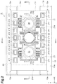
FIG. 2 is a plan view of a mirror unit illustrate inFIG. 1 . -
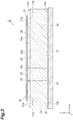
FIG. 3 is a cross-sectional view of the mirror unit along line III-III inFIG. 2 . -
FIG. 4 is a cross-sectional view of the mirror unit along line IV-IV inFIG. 2 . -
FIG. 5 is a schematic cross-sectional view of the mirror device along line V-V inFIG. 2 . -
FIG. 6 is a partially enlarged view of the mirror device illustrated inFIG. 2 . -
FIG. 7 is a plan view of an optical function member illustrated inFIG. 2 . -
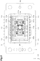
FIG. 8 is a cross-sectional view of the optical module along line VIII-VIII inFIG. 1 . -
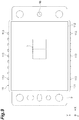
FIG. 9 is a cross-sectional view of the optical module along line IX-IX inFIG. 1 . -
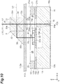
FIG. 10 is a schematic cross-sectional view of a mirror unit and a beam splitter unit illustrated inFIG. 1 . -
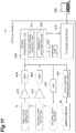
FIG. 11 is a block diagram illustrating a configuration of the optical module illustrated inFIG. 1 . -
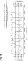
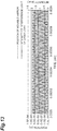
FIG. 12 is a graph illustrating a temporal variation of a position of a movable mirror that resonates, and a temporal variation of the intensity of interference light of measurement light. -
FIG. 13 is a graph illustrating a temporal variation of the position of the movable mirror that resonates, and a temporal variation of the intensity of interference light of laser light. -
FIG. 14 is a graph illustrating the temporal variation of the position of the movable mirror that resonates, and a voltage signal. -
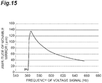
FIG. 15 is a graph illustrating a relationship between a frequency of the voltage signal and an amplitude of the movable mirror. -
FIG. 16 is a graph illustrating a relationship between a rectangular wave that is input to each of a High terminal and a Low terminal of an HVIC, and a voltage signal output from an output terminal of the HVIC. -
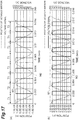
FIG. 17 is a graph illustrating the temporal variation of the position of the movable mirror that resonates, and a voltage signal.- (a) of
FIG. 18 is a graph illustrating the temporal variation of the intensity of interference light of measurement light and (b) ofFIG. 18 is a graph illustrating the temporal variation of the intensity of the interference light of laser light. - (a) of
FIG. 19 is graph illustrating the temporal variation of the intensity of the interference light of the measurement light and voltage logic, and (b) ofFIG. 19 is a graph illustrating the temporal variation of the intensity of the interference light of the laser light, and voltage logic. - (a) of
FIG. 20 is a graph illustrating the temporal variation of the intensity of the interference light of the measurement light, and LSB logic, and (b) ofFIG. 20 is a graph illustrating the temporal variation of the intensity of the interference light of the laser light, and the LSB logic.
- (a) of
-
FIG. 21 is a graph illustrating the temporal variation of the intensity of the interference light of the measurement light, and the temporal variation of the intensity of the interference light of the laser light. -
FIG. 22 is a block diagram illustrating a configuration of a storage unit illustrated inFIG. 11 . -
FIG. 23 is a graph illustrating a temporal variation of an average value of first measurement light intensity, and a temporal variation of an average value of first laser light intensity. -
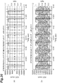
FIG. 24 is a graph illustrating a temporal variation of an average value of second measurement light intensity, and a temporal variation of an average value of second laser light intensity with respect to odd-numbered cycles. -
FIG. 25 is a graph illustrating a part of the temporal variation illustrated inFIG. 23 . -
FIG. 26 is a graph illustrating a relationship between an optical path difference and a first intensity value. -
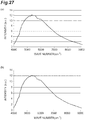
FIG. 27 is a graph illustrating a spectrum of the measurement light. -
FIG. 28 is a graph illustrating a voltage signal of a modification example. -
FIG. 29 is a block diagram illustrating a configuration of a storage unit of the modification example. -
FIG. 30 is a block diagram illustrating a configuration of an optical module of the modification example. -
FIG. 31 is a graph illustrating a capacitance signal and a voltage signal. -
FIG. 32 is a graph illustrating the temporal variation of the intensity of the interference light of the measurement light and the voltage signal. -
FIG. 33 is a block diagram illustrating a configuration of a system provided with the optical module illustrated inFIG. 1 . -
FIG. 34 is a cross-sectional view of the optical module of the modification example. -
FIG. 35 is a configuration diagram of an interference optical system of the modification example. -
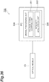
FIG. 36 is a configuration diagram of a signal processing system of the embodiment. - Hereinafter, embodiments of the present disclosure will be described in detail with reference to the accompanying drawings. Note that, the same reference numeral will be given to the same or equivalent portion in the drawings, and redundant description thereof will be omitted.
- As illustrated in
FIG. 1 , anoptical module 1A includes amirror unit 2, abeam splitter unit 3, alight incident unit 4, afirst light detector 6, a secondlight source 7, a secondlight detector 8, asupport 9, afirst support structure 11, and asecond support structure 12. Themirror unit 2 is disposed on one side of thesupport 9 in a Z-axis direction (a first direction), and is attached to thesupport 9, for example, by an adhesive. For example, thesupport 9 is formed of copper tungsten, and has a rectangular plate shape. Themirror unit 2 includes amovable mirror 22 that moves along the Z-axis direction, and a fixedmirror 16 of which a position is fixed (details thereof will be described later). Note that, for example, the Z-axis direction is a vertical direction, and the one side in the Z-axis direction is an upper side. - The
beam splitter unit 3 is disposed on one side of themirror unit 2 in the Z-axis direction, and is supported by thefirst support structure 11. For example, thefirst support structure 11 is attached to thesupport 9 by an adhesive. Thelight incident unit 4 is disposed on one side of thebeam splitter unit 3 in an X-axis direction (a second direction intersecting the first direction), and is supported by thesecond support structure 12. Thefirst light detector 6, the secondlight source 7, and the secondlight detector 8 are disposed on one side of thebeam splitter unit 3 in the Z-axis direction, and are supported by thesecond support structure 12. For example, thesecond support structure 12 is attached to thesupport 9 by a bolt. - In the
optical module 1A, an interference optical system is constituted by thebeam splitter unit 3, themovable mirror 22, and the fixedmirror 16 with respect to each of measurement light L0 and laser light L10. The interference optical system which is constituted with respect to each of the measurement light L0 and the laser light L10 is, for example, a Michelson interference optical system. - With regard to the measurement light L0, interference light L1 of measurement light is detected as follows. That is, when the measurement light L0 that is incident from a first light source (not illustrated) through a measurement target (not illustrated) or the measurement light L0 that is generated from the measurement target (for example, light emitted from the measurement target itself, or the like) is incident to the
beam splitter unit 3 from thelight incident unit 4, the measurement light L0 is divided into a part and the remainder in thebeam splitter unit 3. Then, the part of the measurement light L0 is reflected by themovable mirror 22 that reciprocates in the Z-axis direction, and returns to thebeam splitter unit 3. On the other hand, the remainder of the measurement light L0 is reflected by the fixedmirror 16 and returns to thebeam splitter unit 3. The part and the remainder of the measurement light L0, which return to thebeam splitter unit 3, are emitted from thebeam splitter unit 3 as the interference light L1, and the interference light L1 of the measurement light is detected by thefirst light detector 6. - With regard to the laser light L10, interference light L11 of laser light is detected as follows. That is, when the laser light L10 emitted from the second
light source 7 is incident to thebeam splitter unit 3, the laser light L10 is divided into a part and the remainder in thebeam splitter unit 3. Then, the part of the laser light L10 is reflected by themovable mirror 22 that reciprocates in the Z-axis direction, and returns to thebeam splitter unit 3. On the other hand, the remainder of the laser light L10 is reflected by the fixedmirror 16 and returns to thebeam splitter unit 3. The part and the remainder of the laser light L10, which return to thebeam splitter unit 3, are emitted from thebeam splitter unit 3 as the interference light L11, and the interference light L11 of the laser light is detected by the secondlight detector 8. - According to the
optical module 1A, measurement of a position of themovable mirror 22 in the Z-axis direction can be measured based on a detection result of the interference light L11 of the laser light, and spectral analysis with respect to the measurement target can be performed based on a measurement result of the position, and a detection result of the interference light L1 of the measurement light. - As illustrated in
FIG. 2 ,FIG. 3 , andFIG. 4 , themirror unit 2 includes amirror device 20, anoptical function member 13, a fixedmirror 16, and astress mitigation substrate 17. Themirror device 20 includes abase 21, amovable mirror 22, and adrive unit 23. - The
base 21 includes afirst surface 21a (surface on one side in the Z-axis direction), and asecond surface 21b opposite to thefirst surface 21a. Each of thefirst surface 21a and thesecond surface 21b is a main surface of thebase 21. For example, thebase 21 has a rectangular plate shape, and a size of approximately 10 mm × 15 mm × 0.35 mm (thickness). Themovable mirror 22 includes amirror surface 22a and amovable unit 22b in which amirror surface 22a is provided. Themovable mirror 22 is supported in the base 21 to be movable along the Z-axis direction (the first direction interesting the first surface) perpendicular to thefirst surface 21a. Thedrive unit 23 is configured to move themovable mirror 22 along the Z-axis direction. - The
mirror device 20 is provided with a pair oflight passage portions light passage portions movable mirror 22 in the X-axis direction. Thelight passage portion 24 constitutes a first portion of an optical path between thebeam splitter unit 3 and the fixedmirror 16. Note that, in this embodiment, thelight passage portion 25 does not function as a light passage portion. - Here, a configuration of the
mirror device 20 will be described in detail with reference toFIG. 2 ,FIG. 5 , andFIG. 6 . Note that,FIG. 5 is a schematic cross-sectional view of themirror device 20 illustrated inFIG. 3 , andFIG. 5 schematically illustrates themirror device 20, for example, in a state in which dimensions in the Z-axis direction are enlarged in comparison to actual dimensions. - The
base 21, themovable unit 22b of themovable mirror 22, and thedrive unit 23 are constituted by a silicon on insulator (SOI) substrate (semiconductor substrate) 100. That is, themirror device 20 is a micro electro mechanical systems (MEMS) device constituted by theSOI substrate 100. For example, themirror device 20 is formed in a rectangular plate shape. TheSOI substrate 100 includes asupport layer 101, adevice layer 102, and anintermediate layer 103. Thesupport layer 101 is a first silicon layer (a first semiconductor layer). Thedevice layer 102 is a second silicon layer (a second semiconductor layer). Theintermediate layer 103 is an insulating layer that is disposed between thesupport layer 101 and thedevice layer 102. TheSOI substrate 100 includes thesupport layer 101, theintermediate layer 103, and thedevice layer 102 in this order from the one side in the Z-axis direction. - The
base 21 is constituted by a part of thesupport layer 101, thedevice layer 102, and theintermediate layer 103. Thefirst surface 21a of thebase 21 is a surface of thesupport layer 101 which is opposite to theintermediate layer 103. Thesecond surface 21b of thebase 21 is a surface of thedevice layer 102 which is opposite to theintermediate layer 103. Thesupport layer 101 that constitutes thebase 21 is thicker than thedevice layer 102 that constitutes thebase 21. For example, the thickness of thesupport layer 101 that constitutes thebase 21 is approximately four times the thickness of thedevice layer 102 that constitutes thebase 21. As will be described later, in themirror unit 2, thesecond surface 21b of thebase 21 and athird surface 13a of theoptical function member 13 are joined to each other (refer toFIG. 3 andFIG. 4 ). - The
movable mirror 22 is disposed in a state in which an intersection between an axial line R1 and an axial line R2 is set as the central position (gravity center position). The axial line R1 is a straight line that extends in the X-axis direction. The axial line R2 is a straight line that extends in a Y-axis direction. When viewed from the Z-axis direction, in themirror device 20, a portion other than a portion that overlaps asixth surface 21d of the base 21 to be described later has a shape that is linearly symmetric to each of the axial line R1 and the axial line R2. - The movable mirror 22 (
movable unit 22b) includes anarrangement portion 221, aframe portion 222, a pair ofconnection portions 223, and abeam portion 224. Thearrangement portion 221, theframe portion 222, and the pair ofconnection portions 223 are constituted by a part of thedevice layer 102. Thearrangement portion 221 has a circular shape when viewed from the Z-axis direction. Thearrangement portion 221 includes acentral portion 221a and anedge portion 221b. For example, themirror surface 22a is provided on a surface 221as of thecentral portion 221a on the one side in the Z-axis direction by forming a metal film (metal layer) thereon. Themirror surface 22a extends perpendicular to the Z-axis direction, and has a circular shape. The surface 221as of thecentral portion 221a is a surface on theintermediate layer 103 side in thedevice layer 102. Themirror surface 22a is located on the other side in the Z-axis direction in comparison to thefirst surface 21a of thebase 21. In other words, thefirst surface 21a is located on the one side in the Z-axis direction in comparison to themirror surface 22a. Theedge portion 221b surrounds thecentral portion 221a when viewed from the Z-axis direction. - The
frame portion 222 extends in an annular shape to surround thearrangement portion 221 with a predetermined gap from thearrangement portion 221 when viewed from the Z-axis direction. For example, theframe portion 222 has a circular ring shape when viewed from the Z-axis direction. Each of the pair ofconnection portions 223 connects thearrangement portion 221 and theframe portion 222 to each other. The pair ofconnection portions 223 are respectively disposed on both sides of thearrangement portion 221 in the Y-axis direction. - The
beam portion 224 is constituted by thesupport layer 101 and theintermediate layer 103 which are disposed on thedevice layer 102. Thebeam portion 224 includes aninner beam portion 224a, anouter beam portion 224b, and a pair ofconnection beam portions 224c. Theinner beam portion 224a is disposed on a surface of theedge portion 221b on the one side in the Z-axis direction. Theinner beam portion 224a surrounds themirror surface 22a when viewed from the Z-axis direction. For example, an outer edge of theinner beam portion 224a extends along an outer edge of thearrangement portion 221 with a predetermined gap from the outer edge of thearrangement portion 221 when viewed from the Z-axis direction. An inner edge of theinner beam portion 224a extends along an outer edge of themirror surface 22a with a predetermined gap from the outer edge of themirror surface 22a when viewed from the Z-axis direction. An end surface 224as of theinner beam portion 224a on the one side in the Z-axis direction is located on the one side in the Z-axis direction in comparison to themirror surface 22a. - The
outer beam portion 224b is disposed on a surface of theframe portion 222 on the one side in the Z-axis direction. Theouter beam portion 224b surrounds theinner beam portion 224a and themirror surface 22a when viewed from the Z-axis direction. For example, an outer edge of theouter beam portion 224b extends along an outer edge of theframe portion 222 with a predetermined gap from the outer edge of theframe portion 222 when viewed from the Z-axis direction. An inner edge of theouter beam portion 224b extends along an inner edge of theframe portion 222 with a predetermined gap from the inner edge of theframe portion 222 when viewed from the Z-axis direction. An end surface 224bs of theouter beam portion 224b on the one side in the Z-axis direction is located on the one side in the Z-axis direction in comparison to themirror surface 22a. - The pair of
connection beam portions 224c are respectively disposed on surfaces of the pair ofconnection portions 223 on the one side in the Z-axis direction. Theconnection beam portions 224c connect theinner beam portion 224a and theouter beam portion 224b to each other. End surfaces 224cs of theconnection beam portions 224c on the one side in the Z-axis direction are located on the one side in the Z-axis direction in comparison to themirror surface 22a. - The thickness of the
inner beam portion 224a, the thickness of theouter beam portion 224b, and the thickness of the respectiveconnection beam portions 224c in the Z-axis direction are the same as each other. That is, the thickness of thesupport layer 101 that constitutes theinner beam portion 224a, theouter beam portion 224b, and the respectiveconnection beam portions 224c is the same in each case. The end surface 224as of theinner beam portion 224a, the end surface 224bs of theouter beam portion 224b, and the end surfaces 224cs of the respectiveconnection beam portions 224c are located on the same plane perpendicular to the Z-axis direction. Thesupport layer 101 that constitutes theinner beam portion 224a, theouter beam portion 224b, and the respectiveconnection beam portions 224c is thinner than thesupport layer 101 that constitutes thebase 21. Accordingly, the end surfaces 224as, 224bs, and 224cs are located on the one side in the Z-axis direction in comparison to thefirst surface 21a of thebase 21. In other words, thefirst surface 21a is located on the other side in the Z-axis direction in comparison to the end surfaces 224as, 224bs, and 224cs. - When viewed from the Z-axis direction, a width of the
outer beam portion 224b is wider than a width of theinner beam portion 224a. The width of theinner beam portion 224a when viewed from the Z-axis direction is a length of theinner beam portion 224a in a direction perpendicular to the extending direction of theinner beam portion 224a, and is a length of theinner beam portion 224a in a radial direction of theinner beam portion 224a in this embodiment. This is also true of a width of theouter beam portion 224b when viewed from the Z-axis direction. A width of each of theconnection beam portions 224c is wider than the width of each of theinner beam portion 224a and theouter beam portion 224b. The width of each of theconnection beam portion 224c is a length of each of theconnection beam portion 224c along the extending direction of theinner beam portion 224a. - The
drive unit 23 includes a first elastic support portion (elastic support portion) 26, a second elastic support portion (elastic support portion) 27, and anactuator unit 28. The firstelastic support portion 26, the secondelastic support portion 27, and theactuator unit 28 are constituted by a part of thedevice layer 102. - Each of the first
elastic support portion 26 and the secondelastic support portion 27 is connected between the base 21 and themovable mirror 22. The firstelastic support portion 26 and the secondelastic support portion 27 support themovable mirror 22 so that the movable mirror 22 (movable unit 22b) is movable in the Z-axis direction (direction intersecting themirror surface 22a). - The first
elastic support portion 26 includes a pair oflevers 261, afirst link member 262, asecond link member 263, a pair ofbeam members 264, anintermediate member 265, a pair of first torsion bars (first torsion support portions) 266, a pair of second torsion bars (second torsion support portions) 267, a pair of non-linearity mitigation springs 268, and a plurality of electrode support portions 269. - The pair of
levers 261 are respectively disposed on both sides of thelight passage portion 24 in the Y-axis direction, and face each other in the Y-axis direction. Each of thelevers 261 has a plate shape that extends along a plane perpendicular to the Z-axis direction. Thelever 261 includes afirst portion 261a, asecond portion 261b that is disposed on a side opposite to themovable mirror 22 with respect to thefirst portion 261a, and athird portion 261c that is connected to thefirst portion 261a and thesecond portion 261b. Thefirst portion 261a and thesecond portion 261b extend in the X-axis direction. A length of thefirst portion 261a in the X-axis direction is shorter than a length of thesecond portion 261b in the X-axis direction. Thethird portions 261c of the pair oflevers 261 obliquely extend to be spaced away from each other as going away from themovable mirror 22. - The
first link member 262 bridges first ends 261d of the pair oflevers 261 on a side opposite to themovable mirror 22. Thefirst link member 262 has a plate shape that extends along a plane perpendicular to the Z-axis direction, and extends in the Y-axis direction. Thesecond link member 263 bridges second ends 261e of the pair oflevers 261 on themovable mirror 22 side. Thesecond link member 263 has a plate shape that extends along a plane perpendicular to the Z-axis direction, and extends in the Y-axis direction. A width of thesecond link member 263 in the X-axis direction is narrower than a width of thefirst link member 262 in the X-axis direction. A length of thesecond link member 263 in the Y-axis direction is shorter than a length of thefirst link member 262 in the Y-axis direction. - The pair of
beam members 264 respectively bridge thesecond portions 261b of the pair oflevers 261 and thefirst link member 262. Therespective beam members 264 have a plate shape that extends along a plane perpendicular to the Z-axis direction. The pair ofbeam members 264 obliquely extend to approach each other as going away from themovable mirror 22. The pair oflevers 261, thefirst link member 262, thesecond link member 263, and the pair ofbeam members 264 define thelight passage portion 24. Thelight passage portion 24 has a polygonal shape when viewed from the Z-axis direction. For example, thelight passage portion 24 is a cavity (hole). Alternatively, a material having optical transparency with respect to the measurement light L0 and the laser light L10 may be disposed in thelight passage portion 24. - The
intermediate member 265 has a plate shape that extends along a plane perpendicular to the Z-axis direction, and extends in the Y-axis direction. Theintermediate member 265 is disposed between themovable mirror 22 and the second link member 263 (in other words, between themovable mirror 22 and the light passage portion 24). Theintermediate member 265 is connected to themovable mirror 22 through the non-linearity mitigation springs 268 as to be described later. - The pair of
first torsion bars 266 respectively bridge thefirst end 261d of onelever 261 and thebase 21, and thefirst end 261d of theother lever 261 and thebase 21. That is, the pair offirst torsion bars 266 are respectively connected between the pair oflevers 261 and thebase 21. Thefirst torsion bars 266 extend in the Y-axis direction. The pair offirst torsion bars 266 are disposed on the same central line parallel to the Y-axis direction. In this embodiment, the central line of thefirst torsion bars 266 and the central line of thefirst link member 262 are located on the same straight line. Aprotrusion 261f that protrudes outward in the Y-axis direction is provided in each of the first ends 261d of thelevers 261, and each of thefirst torsion bars 266 is connected to theprotrusion 261f. - The pair of
second torsion bars 267 respectively bridge thesecond end 261e of onelever 261 and one end of theintermediate member 265, and thesecond end 261e of theother lever 261 and the other end of theintermediate member 265. That is, the pair ofsecond torsion bars 267 are respectively connected between the pair oflevers 261 and themovable mirror 22. The respectivesecond torsion bars 267 extend in the Y-axis direction. The pair ofsecond torsion bars 267 are disposed on the same central line parallel to the Y-axis direction. - The pair of non-linearity mitigation springs 268 are connected between the
movable mirror 22 and theintermediate member 265. That is, the pair of non-linearity mitigation springs 268 are connected between themovable mirror 22 and thesecond torsion bar 267. Each of the non-linearity mitigation springs 268 includes a meanderingportion 268a that extends in a meandering manner when viewed from the Z-axis direction. The meanderingportion 268a includes a plurality ofstraight portions 268b which extend in the Y-axis direction and are aligned in the X-axis direction, and a plurality of foldedportions 268c which alternately connect both ends of the plurality ofstraight portions 268b. One end of the meanderingportion 268a is connected to theintermediate member 265, and the other end of the meanderingportion 268a is connected to theframe portion 222. In the meanderingportion 268a, a portion on theframe portion 222 side has a shape along the outer edge of theframe portion 222. - The
non-linearity mitigation spring 268 is constituted as follows. In a state in which themovable mirror 22 has moved in the Z-axis direction, the amount of deformation of thenon-linearity mitigation spring 268 around the Y-axis direction becomes smaller than the amount of deformation of each of thefirst torsion bar 266 and thesecond torsion bar 267 around the Y-axis direction, and the amount of deformation of thenon-linearity mitigation spring 268 in the X-axis direction becomes larger than the amount of deformation of each of thefirst torsion bar 266 and thesecond torsion bar 267 in the X-axis direction. Accordingly, it is possible to suppress occurrence of non-linearity in twist deformation of thefirst torsion bar 266 and thesecond torsion bar 267, and it is possible to suppress deterioration of control characteristics of themovable mirror 22 due to the non-linearity. Note that, the amount of deformation of thefirst torsion bar 266, thesecond torsion bar 267, and thenon-linearity mitigation spring 268 around the Y-axis direction represents, for example, an absolute value of a twist amount (twist angle). The amount of deformation of thefirst torsion bar 266, thesecond torsion bar 267, and thenon-linearity mitigation spring 268 in the X-axis direction represents, for example, an absolute value of a deflection amount. The amount of deformation of a member around the Y-axis direction represents the amount of deformation of the member in a peripheral direction of a circle of which the center is set to an axial line that passes through the center of the member and is parallel to the Y-axis. This is also true offirst torsion bars 276,second torsion bars 277, and anon-linearity mitigation spring 278 to be described later. - The plurality of electrode support portions 269 include a pair of first electrode support portions 269a, a pair of second electrode support portions 269b, and a pair of third
electrode support portions 269c. Each of theelectrode support portions 269a, 269b, and 269c has a plate shape that extends along a plane perpendicular to the Z-axis direction, and extends in the Y-axis direction. Each of theelectrode support portions 269a, 269b, and 269c extends from thesecond portion 261b of thelever 261 toward a side opposite to thelight passage portion 24. The pair of first electrode support portions 269a are disposed on the same central line parallel to the Y-axis direction. The pair of second electrode support portions 269b are disposed on the same central line parallel to the Y-axis direction. The pair of thirdelectrode support portions 269c are disposed on the same central line parallel to the Y-axis direction. In the X-axis direction, the first electrode support portions 269a, the second electrode support portions 269b, and the thirdelectrode support portions 269c are aligned in this order from themovable mirror 22 side. - The second
elastic support portion 27 includes a pair oflevers 271, afirst link member 272, asecond link member 273, a pair ofbeam members 274, anintermediate member 275, a pair of first torsion bars (first torsion support portions) 276, a pair of second torsion bars (second torsion support portions) 277, a pair of non-linearity mitigation springs 278, and a plurality ofelectrode support portions 279. - The pair of
levers 271 are respectively disposed on both sides of thelight passage portion 25 in the Y-axis direction, and face each other in the Y-axis direction. Each of thelevers 271 has a plate shape that extends along a plane perpendicular to the Z-axis direction. Thelever 271 includes afirst portion 271a, asecond portion 271b that is disposed on a side opposite to themovable mirror 22 with respect to thefirst portion 271a, and athird portion 271c that is connected to thefirst portion 271a and thesecond portion 271b. Thefirst portion 271a and thesecond portion 271b extend in the X-axis direction. A length of thefirst portion 271a in the X-axis direction is shorter than a length of thesecond portion 271b in the X-axis direction. Thethird portions 271c of the pair oflevers 271 obliquely extend to be spaced away from each other as going away from themovable mirror 22. - The
first link member 272 bridges first ends 271d of the pair oflevers 271 on a side opposite to themovable mirror 22. Thefirst link member 272 has a plate shape that extends along a plane perpendicular to the Z-axis direction, and extends in the Y-axis direction. Thesecond link member 273 bridges second ends 271e of the pair oflevers 271 on themovable mirror 22 side. Thesecond link member 273 has a plate shape that extends along a plane perpendicular to the Z-axis direction, and extends in the Y-axis direction. A width of thesecond link member 273 in the X-axis direction is narrower than a width of thefirst link member 272 in the X-axis direction. A length of thesecond link member 273 in the Y-axis direction is shorter than a length of thefirst link member 272 in the Y-axis direction. - The pair of
beam members 274 respectively bridge thesecond portions 271b of the pair oflevers 271 and thefirst link member 272. Therespective beam members 274 have a plate shape that extends along a plane perpendicular to the Z-axis direction. The pair ofbeam members 274 obliquely extend to approach each other as going away from themovable mirror 22. The pair oflevers 271, thefirst link member 272, thesecond link member 273, and the pair ofbeam members 274 define thelight passage portion 25. Thelight passage portion 25 has a polygonal shape when viewed from the Z-axis direction. For example, thelight passage portion 25 is a cavity (hole). Alternatively, a material having optical transparency with respect to the measurement light L0 and the laser light L10 may be disposed in thelight passage portion 25. - The
intermediate member 275 has a plate shape that extends along a plane perpendicular to the Z-axis direction, and extends in the Y-axis direction. Theintermediate member 275 is disposed between themovable mirror 22 and the second link member 273 (in other words, between themovable mirror 22 and the light passage portion 25). Theintermediate member 275 is connected to themovable mirror 22 through the non-linearity mitigation springs 278 as to be described later. - The pair of
first torsion bars 276 respectively bridge thefirst end 271d of onelever 271 and thebase 21, and thefirst end 271d of theother lever 271 and thebase 21. That is, the pair offirst torsion bars 276 are respectively connected between the pair oflevers 271 and thebase 21. Thefirst torsion bars 276 extend in the Y-axis direction. The pair offirst torsion bars 276 are disposed on the same central line parallel to the Y-axis direction. In this embodiment, the central line of thefirst torsion bars 276 and the central line of thefirst link member 272 are located on the same straight line. Aprotrusion 271f that protrudes outward in the Y-axis direction is provided in each of the first ends 271d of thelevers 271, and each of thefirst torsion bars 276 is connected to theprotrusion 271f. - The pair of
second torsion bars 277 respectively bridge thesecond end 271e of onelever 271 and one end of theintermediate member 275, and thesecond end 271e of theother lever 271 and the other end of theintermediate member 275. That is, the pair ofsecond torsion bars 277 are respectively connected between the pair oflevers 271 and themovable mirror 22. The respectivesecond torsion bars 277 extend in the Y-axis direction. The pair ofsecond torsion bars 277 are disposed on the same central line parallel to the Y-axis direction. - The pair of non-linearity mitigation springs 278 are connected between the
movable mirror 22 and theintermediate member 275. That is, the pair of non-linearity mitigation springs 278 are connected between themovable mirror 22 and thesecond torsion bar 277. Each of the non-linearity mitigation springs 278 includes a meanderingportion 278a that extends in a meandering manner when viewed from the Z-axis direction. The meanderingportion 278a includes a plurality ofstraight portions 278b which extend in the Y-axis direction and are aligned in the X-axis direction, and a plurality of foldedportions 278c which alternately connect both ends of the plurality ofstraight portions 278b. One end of the meanderingportion 278a is connected to theintermediate member 275, and the other end of the meanderingportion 278a is connected to theframe portion 222. In the meanderingportion 278a, a portion on theframe portion 222 side has a shape along the outer edge of theframe portion 222. - The
non-linearity mitigation spring 278 is constituted as follows. In a state in which themovable mirror 22 has moved in the Z-axis direction, the amount of deformation of thenon-linearity mitigation spring 278 around the Y-axis direction becomes smaller than the amount of deformation of each of thefirst torsion bar 276 and thesecond torsion bar 277 around the Y-axis direction, and the amount of deformation of thenon-linearity mitigation spring 278 in the X-axis direction becomes larger than the amount of deformation of each of thefirst torsion bar 276 and thesecond torsion bar 277 in the X-axis direction. Accordingly, it is possible to suppress occurrence of non-linearity in twist deformation of thefirst torsion bar 276 and thesecond torsion bar 277, and it is possible to suppress deterioration of control characteristics of themovable mirror 22 due to the non-linearity. - The plurality of
electrode support portions 279 include a pair of firstelectrode support portions 279a, a pair of secondelectrode support portions 279b, and a pair of thirdelectrode support portions 279c. Each of theelectrode support portions electrode support portions second portion 271b of thelever 271 toward a side opposite to thelight passage portion 25. The pair of firstelectrode support portions 279a are disposed on the same central line parallel to the Y-axis direction. The pair of secondelectrode support portions 279b are disposed on the same central line parallel to the Y-axis direction. The pair of thirdelectrode support portions 279c are disposed on the same central line parallel to the Y-axis direction. In the X-axis direction, the firstelectrode support portions 279a, the secondelectrode support portions 279b, and the thirdelectrode support portions 279c are aligned in this order from themovable mirror 22 side. - The
actuator unit 28 moves themovable mirror 22 in the Z-axis direction. Theactuator unit 28 includes a fixed comb electrode (first comb electrode) 281, a movable comb electrode (second comb electrode) 282, a fixed comb electrode (first comb electrode) 283, and a movable comb electrode (second comb electrode) 284. Positions of the fixedcomb electrodes movable comb electrodes movable mirror 22. - The fixed
comb electrode 281 is provided on a part of a surface, which faces the electrode support portions 269, of thedevice layer 102 of thebase 21. The fixedcomb electrode 281 includes a plurality of fixed comb fingers (first comb fingers) 281a which extend along a plane perpendicular to the Y-axis direction. The fixedcomb fingers 281a are aligned in the Y-axis direction with a predetermined gap therebetween. - The
movable comb electrode 282 is provided on a surface of each of the first electrode support portions 269a on themovable mirror 22 side, on surfaces of each of the second electrode support portions 269b on both sides in the X-axis direction, and on a surface of each of the thirdelectrode support portion 269c on themovable mirror 22 side. Themovable comb electrode 282 includes a plurality of movable comb fingers (second comb fingers) 282a which extend along a plane perpendicular to the Y-axis direction. Themovable comb fingers 282a are aligned in the Y-axis direction with a predetermined gap therebetween. - In the fixed
comb electrode 281 and themovable comb electrode 282, the plurality of fixedcomb fingers 281a and the plurality ofmovable comb fingers 282a are alternately arranged. That is, each of the fixedcomb fingers 281a of the fixedcomb electrode 281 is located between themovable comb fingers 282a of themovable comb electrode 282. The fixedcomb fingers 281a and themovable comb fingers 282a, which are adjacent to each other, face each other in the Y-axis direction. A distance between the fixedcomb finger 281a and themovable comb finger 282a, which are adjacent to each other, is approximately several µm. - The fixed
comb electrode 283 is provided on a part of a surface, which faces theelectrode support portions 279, of thedevice layer 102 of thebase 21. The fixedcomb electrode 283 includes a plurality of fixed comb fingers (first comb fingers) 283a which extend along a plane perpendicular to the Y-axis direction. The fixedcomb fingers 283a are aligned in the Y-axis direction with a predetermined gap therebetween. - The
movable comb electrode 284 is provided on a surface of each of the firstelectrode support portion 279a on themovable mirror 22 side, on surfaces of each of the secondelectrode support portions 279b on both sides in the X-axis direction, and on a surface of each of the thirdelectrode support portion 279c on themovable mirror 22 side. Themovable comb electrode 284 includes a plurality of movable comb fingers (second comb fingers) 284a which extend along a plane perpendicular to the Y-axis direction. Themovable comb fingers 284a are aligned in the Y-axis direction with a predetermined gap therebetween. - In the fixed
comb electrode 283 and themovable comb electrode 284, the plurality of fixedcomb fingers 283a and the plurality ofmovable comb fingers 284a are alternately arranged. That is, each of the fixedcomb fingers 283a of the fixedcomb electrode 283 is located between themovable comb fingers 284a of themovable comb electrode 284. The fixedcomb fingers 283a and themovable comb fingers 284a, which are adjacent to each other, face each other in the Y-axis direction. For example, a distance between the fixedcomb finger 283a and themovable comb finger 284a, which are adjacent to each other, is approximately several µm. - The
base 21 is provided with a plurality ofelectrode pads 211. Each of theelectrode pads 211 is disposed on a surface of thedevice layer 102 in anopening 213 formed in thefirst surface 21a of the base 21 up to thedevice layer 102. Several electrode pads among the plurality ofelectrode pads 211 are electrically connected to the fixedcomb electrode 281 or the fixedcomb electrode 283 through thedevice layer 102. Other several electrode pads of the plurality ofelectrode pads 211 are electrically connected to themovable comb electrode 282 or themovable comb electrode 284 through the firstelastic support portion 26 or the secondelastic support portion 27. In addition, thebase 21 is provided with a pair ofelectrode pads 212 capable of being used as a ground electrode. The pair ofelectrode pads 212 are disposed on thefirst surface 21a to be located on both sides of themovable mirror 22 in the Y-axis direction. - In the
mirror device 20 configured as described above, an electric signal for moving themovable mirror 22 along the Z-axis direction is input to thedrive unit 23 through alead pin 113 and a wire (not illustrated) to be described later. Accordingly, for example, an electrostatic force is generated between the fixedcomb electrode 281 and themovable comb electrode 282 which face each other, and between the fixedcomb electrode 283 and themovable comb electrode 284 which face each other so that themovable mirror 22 moves to one side in the Z-axis direction. At this time,first torsion bars second torsion bars elastic support portion 26 and the secondelastic support portion 27 are twisted, and an elastic force is generated in the firstelastic support portion 26 and the secondelastic support portion 27. In themirror device 20, when a periodic electric signal is applied to thedrive unit 23, it is possible to reciprocate themovable mirror 22 in the Z-axis direction at a resonance frequency level. In this manner, thedrive unit 23 functions as an electrostatic actuator. - As illustrated in
FIG. 2 ,FIG. 3 ,FIG. 4 , andFIG. 7 , theoptical function member 13 includes thethird surface 13a (surface on one side in the Z-axis direction) facing thesecond surface 21b of thebase 21, and afourth surface 13b on a side opposite to thethird surface 13a. When viewed from the Z-axis direction, anouter edge 13c of theoptical function member 13 is located on an outer side of anouter edge 21c of thebase 21. That is, when viewed from the Z-axis direction, theouter edge 13c of theoptical function member 13 surrounds theouter edge 21c of thebase 21. Theoptical function member 13 is integrally formed by a material having optical transparency with respect to the measurement light L0 and the laser light L10. For example, theoptical function member 13 is formed of glass in a rectangular plate shape, and has a size of approximately 15 mm × 20 mm × 4 mm (thickness). Note that, the material of theoptical function member 13 is selected in accordance with a sensitivity wavelength of theoptical module 1A. For example, glass is selected in a case where the sensitivity wavelength of theoptical module 1A is a near infrared region, and silicon is selected in a case where the sensitivity wavelength of theoptical module 1A is a middle infrared region. - The
optical function member 13 is provided with a pair of light transmittingportions optical function member 13, thelight transmitting portion 14 is a portion that faces thelight passage portion 24 of themirror device 20 in the Z-axis direction. In theoptical function member 13, thelight transmitting portion 15 is a portion that faces thelight passage portion 25 of themirror device 20 in the Z-axis direction. Asurface 14a on themirror device 20 side in thelight transmitting portion 14, and asurface 15a on themirror device 20 side in thelight transmitting portion 15 are flush with thethird surface 13a. Thelight transmitting portion 14 constitutes a second portion of an optical path between thebeam splitter unit 3 and the fixedmirror 16. Thelight transmitting portion 14 is a portion that corrects an optical path difference that occurs between an optical path between thebeam splitter unit 3 and themovable mirror 22, and an optical path between thebeam splitter unit 3 and the fixedmirror 16. Note that, in this embodiment, thelight transmitting portion 15 does not function as a light transmitting portion. - The
optical function member 13 includes afifth surface 13d that faces themovable mirror 22 and thedrive unit 23 of themirror device 20. Thefifth surface 13d is located on thefourth surface 13b side in comparison to thethird surface 13a. Thefifth surface 13d extends up to theouter edge 13c of theoptical function member 13 when viewed from the Z-axis direction. In this embodiment, thefifth surface 13d extends up to each of a pair of opposite sides extending in the Y-axis direction (direction intersecting the first direction and the second direction) in theouter edge 13c of theoptical function member 13 while surrounding an end of each of thelight transmitting portions mirror device 20 side. - The
third surface 13a of theoptical function member 13 is joined to thesecond surface 21b of the base 21 by direct bonding (for example, plasma activation bonding, surface-activated room-temperature bonding (SAB), atomic diffusion bonding (ADB), anodic bonding, fusion bonding, hydrophilic bonding, and the like). In this embodiment, thethird surface 13a extends to face the plurality ofelectrode pads base 21 on both side of thefifth surface 13d in the Y-axis direction. Here, thefifth surface 13d is located on thefourth surface 13b side in comparison to thethird surface 13a, and thus thefifth surface 13d is spaced apart from themirror device 20 in a region facing themovable mirror 22 and thedrive unit 23. In addition, thesurface 14a of thelight transmitting portion 14 and thesurface 15a of thelight transmitting portion 15 face thelight passage portions mirror device 20, respectively. According to this, in themirror unit 2, when themovable mirror 22 reciprocates along the Z-axis direction, themovable mirror 22 and thedrive unit 23 are prevented from coming into contact with theoptical function member 13. - Note that, the
base 21 of themirror device 20 is provided with asixth surface 21d that is spaced apart from theoptical function member 13 in a state in which thethird surface 13a of theoptical function member 13 and thesecond surface 21b of the base 21 are joined to each other. Thesixth surface 21d is spaced apart from theoptical function member 13 in a region including at least a part of the outer edge of the base 21 when viewed from the Z-axis direction. In this embodiment, thesixth surface 21d is formed by etching and removing thedevice layer 102 and theintermediate layer 103 along one side extending in the Y-axis direction in the outer edge of thebase 21. In addition, a plurality ofreference holes 13e are formed in thethird surface 13a of theoptical function member 13. In this embodiment, the plurality ofreference holes 13e are formed in thethird surface 13a to correspond a plurality of corner portions of thebase 21, respectively. When thethird surface 13a of theoptical function member 13 and thesecond surface 21b of the base 21 are joined to each other, a portion corresponding to thesixth surface 21d in thebase 21 is gripped, and handling of themirror device 20 is performed to adjust a position of themirror device 20 in the X-axis direction and the Y-axis direction, and an angle of themirror device 20 in a plane perpendicular to the Z-axis direction on the basis of the plurality ofreference holes 13e formed in thethird surface 13a. - As illustrated in
FIG. 3 andFIG. 4 , the fixedmirror 16 is disposed on a side opposite to themirror device 20 with respect to theoptical function member 13, and a position of themirror device 20 with respect to thebase 21 is fixed. The fixedmirror 16 is formed on thefourth surface 13b of theoptical function member 13, for example, by evaporation. The fixedmirror 16 has amirror surface 16a perpendicular to the Z-axis direction. In this embodiment, themirror surface 22a of themovable mirror 22 and themirror surface 16a of the fixedmirror 16 face one side (beam splitter unit 3 side) in the Z-axis direction. Note that, the fixedmirror 16 is formed continuously to thefourth surface 13b of theoptical function member 13 to reflect light transmitted through each of thelight transmitting portions optical function member 13, but a fixed mirror that reflects light transmitted through thelight transmitting portion 14 and a fixed mirror that reflects light transmitted through thelight transmitting portion 15 may be provided, respectively. - The
stress mitigation substrate 17 is attached to thefourth surface 13b of theoptical function member 13 through the fixedmirror 16. Thestress mitigation substrate 17 is attached to the fixedmirror 16, for example, by an adhesive. When viewed from the Z-axis direction, an outer edge of thestress mitigation substrate 17 is located on an outer side of theouter edge 13c of theoptical function member 13. That is, when viewed from the Z-axis direction, the outer edge of thestress mitigation substrate 17 surrounds theouter edge 13c of theoptical function member 13. A thermal expansion coefficient of thestress mitigation substrate 17 is closer to a thermal expansion coefficient of thebase 21 of the mirror device 20 (more specifically, a thermal expansion coefficient of the support layer 101) in comparison to a thermal expansion coefficient of theoptical function member 13. In addition, the thickness of thestress mitigation substrate 17 is closer to the thickness of thebase 21 of themirror device 20 in comparison to the thickness of theoptical function member 13. For example, thestress mitigation substrate 17 is formed of silicon in a rectangular plate shape, and has a size of approximately 16 mm × 21 mm × 0.65 mm (thickness). - As illustrated in
FIG. 1 , themirror unit 2 configured as described above is attached to thesupport 9 by fixing a surface on a side opposite to theoptical function member 13 in thestress mitigation substrate 17 to asurface 9a (surface on one side in the Z-axis direction) of thesupport 9, for example, by an adhesive. Whenmirror unit 2 is attached to thesupport 9, as illustrated inFIG. 8 , the position of themirror device 20 in the X-axis direction and the Y-axis direction, and the angle of themirror device 20 in a plane perpendicular to the Z-axis direction are adjusted on the basis of areference holes 9b formed in thesupport 9. Note that, inFIG. 8 , thesecond support structure 12 is not illustrated. - As illustrated in
FIG. 1 andFIG. 8 , thefirst support structure 11 includes aframe body 111, alight transmitting member 112, and a plurality of lead pins 113. Theframe body 111 is formed to surround themirror unit 2 when viewed from the Z-axis direction, and is attached to thesurface 9a of thesupport 9, for example, by an adhesive such as silver solder. For example, theframe body 111 is formed of ceramic, and has a rectangular frame shape. Anend surface 111a opposite to thesupport 9 in theframe body 111 is located on a side opposite to thesupport 9 in comparison to thefirst surface 21a of thebase 21 of themirror device 20. - The
light transmitting member 112 is formed to close an opening of theframe body 111, and is attached to theend surface 111a of theframe body 111, for example, by an adhesive. Thelight transmitting member 112 is formed of a material having optical transparency with respect to the measurement light L0 and the laser light L10, and has, for example, a rectangular plate shape. Here, since theend surface 111a of theframe body 111 is located on a side opposite to thesupport 9 in comparison to thefirst surface 21a of thebase 21 of themirror device 20, thelight transmitting member 112 is spaced apart from themirror device 20. According to this, in theoptical module 1A, when themovable mirror 22 reciprocates along the Z-axis direction, themovable mirror 22 and thedrive unit 23 are prevented from coming into contact with thelight transmitting member 112. Note that, in theoptical module 1A, a package that accommodates themirror unit 2 is constituted by thesupport 9, theframe body 111, and thelight transmitting member 112. - Each of the lead pins 113 is provided in the
frame body 111 so that oneend 113a is located on an inner side of theframe body 111, and the other end (not illustrated) is located on an outer side of theframe body 111. The oneend 113a of each of the lead pins 113 is electrically connected to theelectrode pad lead pin 113 in themirror device 20 by wire (not illustrated). In theoptical module 1A, an electric signal for moving themovable mirror 22 along the Z-axis direction is input to thedrive unit 23 through the plurality of lead pins 113. In this embodiment, astep surface 111b extending in the X-axis direction on both sides of theoptical function member 13 in the Y-axis direction is formed in theframe body 111, and the oneend 113a of thelead pin 113 is disposed on thestep surface 111b. Thelead pin 113 extends in the Z-axis direction on both sides of thesupport 9 in the Y-axis direction, and the other end of thelead pin 113 is located on the other side in the Z-axis direction in comparison to thesupport 9. - As illustrated in
FIG. 10 , thebeam splitter unit 3 is attached to thesurface 112a on a side opposite to themirror device 20 in thelight transmitting member 112, for example, by an optical adhesive that also functions as a refractive index matching agent. Thebeam splitter unit 3 includes a first mirror surface (beam splitter) 31, asecond mirror surface 32, and a plurality ofoptical surfaces beam splitter unit 3 is constituted by joining a plurality ofoptical blocks optical function member 13. Note that,FIG. 10 is a schematic cross-sectional view of themirror unit 2 and thebeam splitter unit 3 illustrated inFIG. 1 , and inFIG. 10 , themirror device 20 is schematically illustrated, for example, in a state in which dimensions in the Z-axis direction are enlarged in comparison to actual dimensions. - The
first mirror surface 31 is a mirror surface (for example, a half mirror surface) that is inclined with respect to the Z-axis direction, and is formed between theoptical block 34 and theoptical block 35. In this embodiment, thefirst mirror surface 31 is a surface that is parallel to the Y-axis direction, has an angle of 45° with respect to the Z-axis direction, and is inclined to be spaced away from thelight incident unit 4 as it approaches themirror device 20. Thefirst mirror surface 31 has a function of reflecting a part of the measurement light L0 and allowing the remainder of the measurement light L0 to be transmitted therethrough, and a function of reflecting a part of the laser light L10 and allowing the remainder of the laser light L10 to be transmitted therethrough. For example, thefirst mirror surface 31 is formed of a dielectric multi-layer film. Thefirst mirror surface 31 overlaps thelight passage portion 24 of themirror device 20, thelight transmitting portion 14 of theoptical function member 13, and themirror surface 16a of the fixedmirror 16 when viewed from the Z-axis direction, and overlaps thelight incident unit 4 when viewed from the X-axis direction (refer toFIG. 1 ). That is, thefirst mirror surface 31 faces the fixedmirror 16 in the Z-axis direction, and faces thelight incident unit 4 in the X-axis direction. - The
second mirror surface 32 is a mirror surface (for example, a total reflection mirror surface) that is parallel to thefirst mirror surface 31, and is formed in theoptical block 36 to be located on a side opposite to thelight incident unit 4 with respect to thefirst mirror surface 31. Thesecond mirror surface 32 has a function of reflecting the measurement light L0 and a function of reflecting the laser light L10. For example, thesecond mirror surface 32 is formed of a metal film. Thesecond mirror surface 32 overlaps themirror surface 22a of themovable mirror 22 of themirror device 20 when viewed from the Z-axis direction, and overlaps thefirst mirror surface 31 when viewed from the X-axis direction. That is, thesecond mirror surface 32 faces themovable mirror 22 in the Z-axis direction, and faces thefirst mirror surface 31 in the X-axis direction. - The
optical surface 33a is a surface perpendicular to the Z-axis direction, and is formed in theoptical block 35 to be located on a side opposite to themirror device 20 with respect to thefirst mirror surface 31. Theoptical surface 33b is a surface perpendicular to the Z-axis direction, and is formed in theoptical block 36 to be located on themirror device 20 side with respect to thesecond mirror surface 32. Theoptical surface 33c is a surface perpendicular to the Z-axis direction, and is formed in theoptical block 34 to be located on themirror device 20 side with respect to thefirst mirror surface 31. Theoptical surface 33b and theoptical surface 33c are located on the same plane. Theoptical surface 33d is a surface perpendicular to the X-axis direction, and is formed in theoptical block 34 to be located on thelight incident unit 4 side with respect to thefirst mirror surface 31. Theoptical surfaces - The
beam splitter unit 3 configured as described above is attached to thelight transmitting member 112 by fixing theoptical surface 33b and theoptical surface 33c which are flush with each other to thesurface 112a of thelight transmitting member 112, for example, by an optical adhesive. When thebeam splitter unit 3 is attached to thelight transmitting member 112, as illustrated inFIG. 9 , the position of thebeam splitter unit 3 in the X-axis direction and the Y-axis direction, and the angle of thebeam splitter unit 3 in a plane perpendicular to the Z-axis direction are adjusted on the basis of thereference holes 9b formed in thesupport 9. Note that, thesecond support structure 12 is not illustrated inFIG. 9 . - Here, an optical path of the measurement light L0 and an optical path of the laser light L10 in the
mirror unit 2 and thebeam splitter unit 3 will be described in detail with reference toFIG. 10 . - As illustrated in
FIG. 10 , when the measurement light L0 is incident to thebeam splitter unit 3 along the X-axis direction through theoptical surface 33d, a part of the measurement light L0 is transmitted through thefirst mirror surface 31, is reflected by thesecond mirror surface 32, and reaches themirror surface 22a of themovable mirror 22 through theoptical surface 33b and thelight transmitting member 112. The part of the measurement light L0 is reflected by themirror surface 22a of themovable mirror 22, proceeds along the same optical path P1 in an opposite direction, and is reflected by thefirst mirror surface 31. The remainder of the measurement light L0 is reflected by thefirst mirror surface 31, and reaches themirror surface 16a of the fixedmirror 16 through theoptical surface 33c, thelight transmitting member 112, thelight passage portion 24 of themirror device 20, and thelight transmitting portion 14 of theoptical function member 13. The remainder of the measurement light L0 is reflected by themirror surface 16a of the fixedmirror 16, proceeds along the same optical path P2 in an opposite direction, and is transmitted through thefirst mirror surface 31. The part of the measurement light L0 which is reflected by thefirst mirror surface 31, and the remainder of the measurement light L0 which is transmitted through thefirst mirror surface 31 become interference light L1, and the interference light L1 of the measurement light is emitted from thebeam splitter unit 3 through theoptical surface 33a along the Z-axis direction. - On the other hand, when the laser light L10 is incident to the
beam splitter unit 3 through theoptical surface 33a along the Z-axis direction, a part of the laser light L10 is reflected by thefirst mirror surface 31 and thesecond mirror surface 32, and reaches themirror surface 22a of themovable mirror 22 through theoptical surface 33b and thelight transmitting member 112. The part of the laser light L10 is reflected by themirror surface 22a of themovable mirror 22, proceeds along the same optical path P3 in an opposite direction, and is reflected by thefirst mirror surface 31. The remainder of the laser light L10 is transmitted through thefirst mirror surface 31, and reaches themirror surface 16a of the fixedmirror 16 through theoptical surface 33c, thelight transmitting member 112, thelight passage portion 24 of themirror device 20, and thelight transmitting portion 14 of theoptical function member 13. The remainder of the laser light L10 is reflected by themirror surface 16a of the fixedmirror 16, proceeds along the same optical path P4 in an opposite direction, and is transmitted through thefirst mirror surface 31. The part of the laser light L10 reflected by thefirst mirror surface 31 and the remainder of the laser light L10 transmitted through thefirst mirror surface 31 become interference light L11, and the interference light L11 of the laser light is emitted from thebeam splitter unit 3 through theoptical surface 33a along the Z-axis direction. - As described above, the
light passage portion 24 of themirror device 20 constitutes a first portion P2a of the optical path P2 of the measurement light L0 and a first portion P4a of the optical path P4 of the laser light L10 in an optical path between thebeam splitter unit 3 and the fixedmirror 16. In addition, thelight transmitting portion 14 of theoptical function member 13 constitutes a second portion P2b of the optical path P2 of the measurement light L0 and a second portion P4b of the optical path P4 of the laser light L10 in an optical path between thebeam splitter unit 3 and the fixedmirror 16. - The second portion P2b of the optical path P2 of the measurement light L0 is constituted by the
light transmitting portion 14, and thus an optical path difference between the optical paths P1 and P2 is corrected so that a difference between an optical path length (an optical path length in consideration of a refractive index of respective media through which the optical path passes) of the optical path P1 of the measurement light L0 and an optical path length of the optical path P2 of the measurement light L0 decreases. Similarly, the second portion P4b of the optical path P4 of the laser light L10 is constituted by thelight transmitting portion 14, and thus an optical path difference between the optical paths P3 and P4 is corrected so that a difference between an optical path length of the optical path P3 of the laser light L10 and an optical path length of the optical path P4 of the laser light L10 decreases. In this embodiment, a refractive index of thelight transmitting portion 14 is equal to a refractive index of theoptical blocks beam splitter unit 3, and a distance between thefirst mirror surface 31 and thesecond mirror surface 32 along the X-axis direction is equal to the thickness of thelight transmitting portion 14 along the Z-axis direction (that is, a distance between thesurface 14a of thelight transmitting portion 14 and thefourth surface 13b of theoptical function member 13 along the Z-axis direction). - In the
optical module 1A, a zero optical path difference position C0 deviates from a central position C1 of a resonance operation (reciprocating operation in a resonance frequency) of themovable mirror 22 in themirror device 20. The zero optical path difference position C0 represents a position of themovable mirror 22 at which an optical path length on themovable mirror 22 side with which the interference light L1 of the measurement light is caused to occur becomes the same as an optical path length on the fixedmirror 16 side with which the interference light L1 of the measurement light is caused to occur. In this embodiment, the zero optical path difference position C0 is a position of themovable mirror 22 at which an optical path length between thefirst mirror surface 31 of thebeam splitter unit 3 and themirror surface 22a of the movable mirror 22 (that is, an optical path length of the optical paths P1 and P3) becomes the same as an optical path length between thefirst mirror surface 31 of thebeam splitter unit 3 and themirror surface 16a of the fixed mirror 16 (that is, an optical path length of the optical paths P2 and P4). The amount of deviation of the zero optical path difference position C0 to the central position C1 is smaller than an amplitude of the resonance operation of themovable mirror 22. In this embodiment, the zero optical path difference position C0 is the same as a position of thesurface 14a of thelight transmitting portion 14 in the Z-axis direction. The central position C1 is a position that deviates from the position of thesurface 14a of thelight transmitting portion 14 in the Z-axis direction to thefirst mirror surface 31 side of thebeam splitter unit 3 along the Z-axis direction by the sum of the thickness of thedevice layer 102 and the thickness of a metal film that constitutes themirror surface 22a. - As illustrated in
FIG. 1 , thesecond support structure 12 includes aconnection unit 120. Theconnection unit 120 includes amain body portion 121, aframe body 122, and afixed plate 123. Themain body portion 121 includes a pair ofside wall portions ceiling wall portion 126. The pair ofside wall portions opening 124a is formed in theside wall portion 124 on one side in the X-axis direction. Theceiling wall portion 126 faces thesupport 9 in the Z-axis direction. Anopening 126a is formed in theceiling wall portion 126. For example, themain body portion 121 is integrally formed of a metal. Themain body portion 121 is provided with a plurality ofpositioning pins 121a. Themain body portion 121 is positioned with respect to thesupport 9 by inserting thepositioning pins 121a intoreference holes support 9, and in this state, themain body portion 121 is attached to thesupport 9, for example, by a bolt. - The
frame body 122 is disposed on a surface on a side opposite to thebeam splitter unit 3 in theside wall portion 124. An opening of theframe body 122 faces thebeam splitter unit 3 through theopening 124a of theside wall portion 124. Thelight incident unit 4 is disposed in theframe body 122. The fixedplate 123 is a member that fixes thelight incident unit 4 disposed in theframe body 122 to themain body portion 121. - The
light incident unit 4 includes aholder 41 and acollimator lens 42. Theholder 41 holds thecollimator lens 42, and is configured so that an optical fiber (not illustrated) that guides the measurement light L0 can be connected to theholder 41. Thecollimator lens 42 collimates the measurement light L0 emitted from the optical fiber. When the optical fiber is connected to theholder 41, an optical axis of the optical fiber matches an optical axis of thecollimator lens 42. - The
holder 41 is provided with aflange portion 41a. Theflange portion 41a is disposed between theframe body 122 and the fixedplate 123. In this state, for example, when the fixedplate 123 is attached to theside wall portion 124, for example, by a bolt, thelight incident unit 4 disposed in theframe body 122 is fixed to themain body portion 121. In this manner, thelight incident unit 4 is disposed on one side of thebeam splitter unit 3 in the X-axis direction, and is supported by thesecond support structure 12. Thelight incident unit 4 allows the measurement light L0 that is incident from the first light source through a measurement target or the measurement light L0 that is generated from the measurement target (in this embodiment, the measurement light L0 guided by the optical fiber) to be incident to thebeam splitter unit 3. - A
filter 54 is attached to theframe body 122. Thefilter 54 has a function of allowing the measurement light L0 to be transmitted therethrough and absorbing the laser light L10. For example, thefilter 54 is formed of silicon in a plate shape. Thefilter 54 is disposed in theopening 124a of theside wall portion 124 in a state of being inclined with respect to an optical axis of thelight incident unit 4. Thefilter 54 closes the opening of theframe body 122 when viewed from the X-axis direction. In this manner, thefilter 54 is disposed between thelight incident unit 4 and thebeam splitter unit 3, and is supported by thesecond support structure 12 in a state of being inclined with respect to the optical axis of thelight incident unit 4. In this embodiment, an optical surface of thefilter 54 is a surface that is parallel to the Z-axis direction and has an angle of 10° to 20° with respect to the Y-axis direction. Note that, the optical axis of thelight incident unit 4 is parallel to the X-axis direction. - The
second support structure 12 further includes a holdingunit 130. The holdingunit 130 includes amain body portion 131. Themain body portion 131 is attached to a surface of theceiling wall portion 126 on a side opposite to thesupport 9. Themain body portion 131 is positioned with respect to themain body portion 121 of theconnection unit 120 by a plurality ofpositioning pins 131a, and in this state, themain body portion 131 is attached to theceiling wall portion 126, for example, by a bolt. A first through-hole 135, a second through-hole 136, and a third through-hole 137 are formed in themain body portion 131. Each of the first through-hole 135, the second through-hole 136, and the third through-hole 137 passes through themain body portion 131 along the Z-axis direction. The first through-hole 135 is formed at a position that faces thefirst mirror surface 31 of thebeam splitter unit 3 in the Z-axis direction. The second through-hole 136 is formed on the other side of the first through-hole 135 in the X-axis direction (that is, on a site opposite to the light incident unit 4). The third through-hole 137 is formed on the other side of the second through-hole 136 in the X-axis direction. - The
first light detector 6 is disposed in the first through-hole 135. Thefirst light detector 6 includes alight detection element 62, apackage 64 including alight transmission window 64a, a holder 61, and a condensinglens 63. Thepackage 64 accommodates thelight detection element 62. Thelight detection element 62 detects the interference light L1 of the measurement light. For example, thelight detection element 62 is an InGaAs photodiode. The holder 61 holds thepackage 64 and the condensinglens 63. The condensinglens 63 condenses the interference light L1 of the measurement light which is incident to thelight detection element 62 through thelight transmission window 64a to thelight detection element 62. An optical axis of thelight detection element 62 and an optical axis of the condensinglens 63 match each other. - The holder 61 is provided with a
flange portion 61a. Theflange portion 61a is positioned with respect to themain body portion 121 of theconnection unit 120 by a positioning pin 61b, and in this state, theflange portion 61a is attached to theceiling wall portion 126 of themain body portion 121, for example, by a bolt. In this manner, thefirst light detector 6 is disposed on one side of thebeam splitter unit 3 in the Z-axis direction, and is supported by thesecond support structure 12. Thefirst light detector 6 faces thefirst mirror surface 31 of thebeam splitter unit 3 in the Z-axis direction. Thefirst light detector 6 detects the interference light L1 of the measurement light which is emitted from thebeam splitter unit 3. - The second
light detector 8 is disposed in the second through-hole 136. The secondlight detector 8 includes alight detection element 82, and apackage 84 including a condensinglens 84a. Thelight detection element 82 detects interference light L11 of the laser light. For example, thelight detection element 82 is a Si photodiode. The condensinglens 84a condenses the interference light L11 of the laser light which is incident to thelight detection element 82 to thelight detection element 82. An optical axis of thelight detection element 82 and an optical axis of the condensinglens 84a match each other. - The
package 84 is fixed to themain body portion 131 in the second through-hole 136. In this manner, the secondlight detector 8 is disposed on the other side (one side of the first optical device in a direction intersecting an optical axis of the first optical device) of thefirst light detector 6 in the X-axis direction to face the same side as in thefirst light detector 6, and is supported by thesecond support structure 12. The secondlight detector 8 detects the interference light L11 of the laser light which is emitted from thebeam splitter unit 3. - The second
light source 7 is disposed in the third through-hole 137. The secondlight source 7 includes a light-emittingelement 72, and apackage 74 including acollimator lens 74a. The light-emittingelement 72 emits the laser light L10. For example, the light-emittingelement 72 is a semiconductor laser such as VCSEL. Thecollimator lens 74a collimates the laser light L10 emitted from the light-emittingelement 72. An optical axis of the light-emittingelement 72 and an optical axis of thecollimator lens 74a match each other. - The
package 74 is fixed to themain body portion 131 in the third through-hole 137. In this manner, the secondlight source 7 is disposed on the other side (one side of the second optical device in a direction intersecting the optical axis of the first optical device) of the secondlight detector 8 in the X-axis direction to face the same side as in thefirst light detector 6, and is supported by thesecond support structure 12. The secondlight source 7 emits the laser light L10 to be incident to thebeam splitter unit 3. - As described above, the holding
unit 130 holds the first light detector (first optical device) 6, the second light detector (second optical device) 8, and the second light source (third optical device) 7 so that thefirst light detector 6, the secondlight detector 8, and the secondlight source 7 face the same side, and are aligned in the order of thefirst light detector 6, the secondlight detector 8, and the secondlight source 7. In this embodiment, the holdingunit 130 holds thefirst light detector 6, the secondlight detector 8, and the secondlight source 7 so that thefirst light detector 6, the secondlight detector 8, and the secondlight source 7 face the other side (that is, thebeam splitter unit 3 side) in the Z-axis direction on one side of thebeam splitter unit 3 in the Z-axis direction. In addition, the holdingunit 130 holds thefirst light detector 6, the secondlight detector 8, and the secondlight source 7 to be aligned in the order of thefirst light detector 6, the secondlight detector 8, and the secondlight source 7 from one side (that is, thelight incident unit 4 side) in the X-axis direction. - Note that, a configuration in which the
first light detector 6 faces an arbitrary side represents that a light-receiving surface of thelight detection element 62 faces the arbitrary side (that is, thefirst light detector 6 is disposed to detect light incident from the arbitrary side). In this case, for example, a lead pin of thelight detection element 62 extends to a side opposite to the arbitrary side. Similarly, a configuration in which the secondlight detector 8 faces an arbitrary side represents that a light-receiving surface of thelight detection element 82 faces the arbitrary side (that is, the secondlight detector 8 is disposed to detect light incident from the arbitrary side). In this case, for example, a lead pin of thelight detection element 82 extends to a side opposite to the arbitrary side. In addition, a configuration in which the secondlight source 7 faces an arbitrary side represents that a light emission surface of the light-emittingelement 72 faces the arbitrary side (that is, the secondlight source 7 is disposed to emit light to the arbitrary side). In this case, for example, a lead pin of the light-emittingelement 72 extends to a side opposite to the arbitrary side. In addition, the holdingunit 130 is a part of thesecond support structure 12, and thus a configuration in which theholding unit 130 holds an arbitrary configuration represents that the arbitrary configuration is supported by thesecond support structure 12. - A
first mirror 51, asecond mirror 52, and athird mirror 53 are attached to themain body portion 121 of theconnection unit 120. Thefirst mirror 51 is attached to theceiling wall portion 126 of themain body portion 121 in theopening 126a to be located on a side opposite to thefirst light detector 6 with respect to the first through-hole 135. Thesecond mirror 52 is attached to theceiling wall portion 126 of themain body portion 121 in theopening 126a to be located on a side opposite to the secondlight detector 8 with respect to the second through-hole 136. Thethird mirror 53 is attached to theceiling wall portion 126 of themain body portion 121 in theopening 126a to be located on a side opposite to the secondlight source 7 with respect to the third through-hole 137. - The
first mirror 51 is a dichroic mirror that has a function of allowing the measurement light L0 to be transmitted therethrough and reflecting the laser light L10, and is inclined with respect to an optical axis of thefirst light detector 6. Thefirst mirror 51 is disposed between thebeam splitter unit 3 and thefirst light detector 6. That is, thefirst mirror 51 is disposed to face thebeam splitter unit 3 and thefirst light detector 6. In this embodiment, an optical surface of thefirst mirror 51 is a surface that is parallel to the Y-axis direction and has an angle of 45° with respect to the Z-axis direction. Note that, an optical axis of thefirst light detector 6 is parallel to the Z-axis direction. - The
second mirror 52 is a mirror (for example, a half mirror) that has a function of reflecting a part of the laser light L10 and allowing the remainder of the laser light L10 to be transmitted therethrough and is parallel to thefirst mirror 51. Thesecond mirror 52 is disposed to overlap thefirst mirror 51 when viewed from the X-axis direction and to overlap the secondlight detector 8 when viewed from the Z-axis direction. That is, thesecond mirror 52 is disposed to face thefirst mirror 51 and the secondlight detector 8. In this embodiment, an optical surface of thesecond mirror 52 is a surface that is parallel to the Y-axis direction, and has an angle of 45° with respect to the Z-axis direction. - The
third mirror 53 is a mirror (for example, a total reflection mirror) that has a function of reflecting the laser light L10 and is parallel to thesecond mirror 52. Thethird mirror 53 is disposed to overlap thesecond mirror 52 when viewed from the X-axis direction, and to overlap the secondlight source 7 when viewed from the Z-axis direction. That is, thethird mirror 53 is disposed to face thesecond mirror 52 and the secondlight source 7. In this embodiment, an optical surface of thethird mirror 53 is a surface that is parallel to the Y-axis direction and has an angle of 45° with respect to the Z-axis direction. - A
filter 56 is disposed between thefirst mirror 51 and thefirst light detector 6. Anaperture 55 is disposed between thefirst mirror 51 and thefilter 56. In this embodiment, theaperture 55 and thefilter 56 are held by the holder 61 of thefirst light detector 6. Theaperture 55 is a member in which an opening having a circular shape is formed when viewed from the Z-axis direction. Thefilter 56 has a function of allowing the measurement light L0 to be transmitted therethrough and absorbing the laser light L10. In this embodiment, thefilter 56 is a member different from a member in which thefirst mirror 51 is formed on a surface (surface facing the beam splitter unit 3) on thebeam splitter unit 3 side. More specifically, thefilter 56 is a silicon plate in which an anti-reflection film is formed, for example, on a light incident surface. In this embodiment, since thefilter 56 is a member different from the member in which thefirst mirror 51 is formed, the degree of freedom of design of each of thefirst mirror 51 and thefilter 56 is improved. - A laser
light absorption unit 57 is disposed on a side opposite to the secondlight detector 8 with respect to thesecond mirror 52. The laserlight absorption unit 57 has a function of absorbing the laser light L10. In this embodiment, the laserlight absorption unit 57 is a part of the second support structure (support) 12 that supports thesecond mirror 52. More specifically, the laserlight absorption unit 57 is a portion that protrudes from theside wall portion 125 of themain body portion 121 of theconnection unit 120 to thebeam splitter unit 3 side. The laserlight absorption unit 57 is constituted by forming a black resist layer on the portion, or by performing a black alumite treatment to the portion. In this embodiment, the laserlight absorption unit 57 is a part of thesecond support structure 12, and thus an increase in the number of parts is suppressed. - Here, description will be given of an optical path between the
beam splitter unit 3 and thefirst light detector 6, and the like. The interference light L1 of the measurement light which is emitted from thebeam splitter unit 3 along the Z-axis direction is transmitted through thefirst mirror 51, is incident to thefirst light detector 6 through theaperture 55 and thefilter 56, and is detected by thefirst light detector 6. On the other hand, the laser light L10 emitted from the secondlight source 7 is reflected by thethird mirror 53 and is transmitted through thesecond mirror 52, and is reflected by thefirst mirror 51 and is incident to thebeam splitter unit 3 along the Z-axis direction. Interference light L11 of the laser light which is emitted from thebeam splitter unit 3 along the Z-axis direction is reflected by thefirst mirror 51 and thesecond mirror 52, and is incident to the secondlight detector 8 and is detected by the secondlight detector 8. Note that, a part of the laser light L10 reflected by thesecond mirror 52 is absorbed by the laserlight absorption unit 57. - In the
optical module 1A, a length of the optical path between thebeam splitter unit 3 and thefirst light detector 6 is shorter than a length of an optical path between thebeam splitter unit 3 and the secondlight detector 8, and is shorter than a length of an optical path between thebeam splitter unit 3 and the secondlight source 7. Note that, the lengths of the optical paths represent physical distances along the optical paths. - Specifically, a distance from an intersection between the optical path and the
first mirror surface 31 of thebeam splitter unit 3 to a light incident surface of thefirst light detector 6 is shorter than a distance from an intersection between an optical path and thefirst mirror surface 31 of thebeam splitter unit 3 to a light incident surface of the secondlight detector 8, and is shorter than a distance from an intersection between an optical path and thefirst mirror surface 31 of thebeam splitter unit 3 to a light emission surface of the secondlight source 7. A distance from an intersection between an optical path and thefirst mirror surface 31 of thebeam splitter unit 3 to a light incident surface of the condensinglens 63 of thefirst light detector 6 is shorter than a distance from an intersection between an optical path and thefirst mirror surface 31 of thebeam splitter unit 3 to a light incident surface of the condensinglens 84a of the secondlight detector 8, and is shorter than a distance from an intersection between an optical path and thefirst mirror surface 31 of thebeam splitter unit 3 to a light emission surface of thecollimator lens 74a of the secondlight source 7. A distance from theoptical surface 33a of thebeam splitter unit 3 to the light incident surface of thefirst light detector 6 is shorter than a distance from theoptical surface 33a of thebeam splitter unit 3 to the light incident surface of the secondlight detector 8, and is shorter than a distance from theoptical surface 33a of thebeam splitter unit 3 to the light emission surface of the secondlight source 7. A distance from theoptical surface 33a of thebeam splitter unit 3 to the light incident surface of the condensinglens 63 of thefirst light detector 6 is shorter than a distance fromoptical surface 33a of thebeam splitter unit 3 to the light incident surface of the condensinglens 84a of the secondlight detector 8, and is shorter than a distance from theoptical surface 33a of thebeam splitter unit 3 to the light emission surface of thecollimator lens 74a of the secondlight source 7. - In this embodiment, the
light incident unit 4 has a configuration in which angle adjustment of theholder 41 with respect to theframe body 122 is possible. In contrast, thefirst light detector 6 is fixed to theceiling wall portion 126 of themain body portion 121, for example, by a bolt in a state of being positioned with respect to themain body portion 121 of theconnection unit 120. Accordingly, in a state in which thefirst light detector 6 is positioned, the angle adjustment of theholder 41 can be carried out so that detection intensity in thefirst light detector 6 becomes the maximum while the measurement light L0 is incident to thebeam splitter unit 3. In addition, in a state in which the angle adjustment is carried out, thelight incident unit 4 can be fixed to theframe body 122. - Note that, not only the
light incident unit 4 but also thefirst light detector 6 may have a configuration in which angle adjustment of the holder 61 is possible. In addition, the secondlight source 7 may have a configuration in which angle adjustment is possible in a state in which the secondlight detector 8 is positioned. In addition, not only the secondlight source 7 but also the secondlight detector 8 may have a configuration in which the angle adjustment is possible. - As illustrated in
FIG. 11 , theoptical module 1A further includes asignal processing unit 200 and astorage unit 300. Thesignal processing unit 200 is electrically connected to each of themirror device 20, the secondlight source 7, thefirst light detector 6, and the secondlight detector 8. For example, thesignal processing unit 200 is an integrated circuit such as a field-programmable gate array (FPGA), and uses a clock divided from a quartz oscillator as a reference clock. Thestorage unit 300 is electrically connected to thesignal processing unit 200. For example, thestorage unit 300 is a non-volatile memory such as an electrically erasable programmable read-only memory (EEPROM). A personal computer (PC) 500 is electrically connected to thesignal processing unit 200 through anexternal interface 410. - The
signal processing unit 200 controls a voltage signal that is applied to the mirror device 20 (specifically, between the fixedcomb electrode 281 and themovable comb electrode 282, and between the fixedcomb electrode 283 and the movable comb electrode 284) by a high voltage generation circuit 401 (details thereof will be described later). For example, the highvoltage generation circuit 401 is a high voltage IC (HVIC). In addition, thesignal processing unit 200 outputs a digital signal for driving the secondlight source 7. The digital signal is converted into an analog signal by a digital-to-analog converter (DAC) 402, and is input to the secondlight source 7. - An analog signal output from the
first light detector 6 is amplified by anamplifier 403, is converted into a digital signal by an analog-to-digital converter (ADC) 404, and is input to thesignal processing unit 200. According to this, thesignal processing unit 200 acquires the digital signal indicating an intensity of the interference light L1 of the measurement light. In addition, an analog signal output from the secondlight detector 8 is amplified by anamplifier 405, is converted into a digital signal by anADC 406, and is input to thesignal processing unit 200. According to this, thesignal processing unit 200 acquires the digital signal indicating an intensity of the interference light L11 of the laser light. - The
signal processing unit 200 includes a voltagesignal control unit 201 and anintensity acquisition unit 202. - The voltage
signal control unit 201 controls a voltage signal so that a voltage signal having a frequency for causing themovable mirror 22 to resonate in themirror device 20 is applied to themirror device 20. The voltage signal is output from the highvoltage generation circuit 401 and is applied to themirror device 20. - Here, the voltage signal control will be described in detail. As a premise, in the
optical module 1A, as illustrated inFIG. 12 , a temporal variation of a position of the movable mirror 22 (position of themovable mirror 22 in the Z-axis direction) that resonates becomes a sinusoidal shape. However, actually, the temporal variation of the position of themovable mirror 22 is not an ideal sinusoidal wave, and a waveform thereof tends to be different between a period T1 in which themovable mirror 22 moves in one direction (for example, a direction approaching the beam splitter unit 3) of reciprocation directions, and a period T2 in which themovable mirror 22 moves in the other direction (for example, a direction being spaced apart from the beam splitter unit 3) of the reciprocation directions. Here, it is desired to perform Fourier transformation type spectral analysis with respect to the intensity (interferogram) of the interference light L1 of the measurement light separately for the period T1 and the period T2. - For the spectral analysis, it is desired to detect a timing of switching from the period T1 to the period T2, and a timing of switching from the period T2 to period T1. The timings correspond to a timing at which a maximum value M1 (for example, a position farthest from the beam splitter unit 3) appears and a timing at which a minimum value M2 (for example, a position closest to the beam splitter unit 3) appears in the temporal variation of the position of the
movable mirror 22, and thus the timings at which the maximum value M1 and the minimum value M2 appear may be detected. However, as illustrated inFIG. 13 , it is difficult to detect the timings at which the maximum value M1 and the minimum value M2 appear from the temporal variation of the intensity of the interference light L11 of the laser light due to a load on arithmetic operation or the like. - Note that, as illustrated in
FIG. 12 , a center burst (CB) in the temporal variation of the intensity of the interference light L1 of the measurement light appears in the first half of the period T1 and the second half of the period T2. The reason for this is that a zero optical path difference position C0 of themovable mirror 22 deviates from the central position C1 of the resonance operation of themovable mirror 22 to a side opposite to thebeam splitter unit 3 as illustrated inFIG. 10 . - On the basis of the premise, the voltage
signal control unit 201 controls a voltage signal that is applied to themirror device 20 so that the Fourier transformation type spectral analysis can be performed with respect to the intensity of the interference light L1 of the measurement light separately in the period T1 and the period T2. Specifically, the voltagesignal control unit 201 controls the voltage signal so that the voltage signal has a frequency two times a resonance frequency of themovable mirror 22 as illustrated inFIG. 14 . The voltage signal is a continuous pulse signal and is a rectangular wave having a duty ratio of 0.5 in this embodiment. - When the voltage signal having a frequency two times the resonance frequency of the
movable mirror 22 is applied to themirror device 20, a rising timing of the voltage signal matches the timings at which the maximum value M1 and the minimum value M2 appear as return positions of themovable mirror 22. Note that, inFIG. 14 , a solid-line arrow represents a movement direction of themovable mirror 22, and a broken-line arrow represents a direction of a force that occurs in themovable mirror 22. In addition, a hatched fixed comb electrode 281 (283) represents a state in which a voltage is applied, and a non-hatched fixed comb electrode 281 (283) represents a state in which a voltage is not applied. - A relationship between the frequency of the voltage signal and an amplitude of the
movable mirror 22 can be acquired by actually causing themirror device 20 to operate. Note that, the relationship between the frequency of the voltage signal and the amplitude of themovable mirror 22 can be predicted, for example, by numerical analysis such as a Runge-Kutta method. In an example of the numerical analysis illustrated inFIG. 15 , when the frequency of the voltage signal is set to 566 Hz, the amplitude of themovable mirror 22 becomes the maximum, and themovable mirror 22 resonates. In this manner, the frequency of the voltage signal for causing themovable mirror 22 to resonate in themirror device 20 is acquired in advance by actual measurement, the numerical analysis, or the like. - As an example, in a case where the high
voltage generation circuit 401 is the HVIC, the voltagesignal control unit 201 adjusts a timing of inputting a rectangular wave to each of a High terminal and a Low terminal of the HVIC with a clock divided from a quartz oscillator set as a reference clock to cause a voltage signal having a desired frequency to be output from an output terminal of the HVIC. As illustrated inFIG. 16 , in the HVIC, a rising timing of a rectangular wave input to the High terminal becomes a rising timing of the voltage signal output from the output terminal, and a rising timing of a rectangular wave input to the Low terminal becomes a falling timing of the voltage signal output from the output terminal. - At the time of initiating an operation of the
movable mirror 22, the voltagesignal control unit 201 operates so that a voltage signal having a frequency two times the resonance frequency of themovable mirror 22 is applied to themirror device 20 from the beginning. Even in this case, since there is an influence such as a manufacturing error of themirror device 20, when waiting reciprocation of themovable mirror 22 for a predetermined number of times (for example, 50 times), it is possible to cause themovable mirror 22 to resonate. Note that, at the time of initiating the operation of themovable mirror 22, the voltagesignal control unit 201 may operate so that the voltage signal that finally has the frequency two times the resonance frequency of themovable mirror 22 is applied to themirror device 20 by reducing the frequency of the voltage signal whenever themovable mirror 22 reciprocates for a predetermined number of times (for example, four times). - When the resonance operation of the
movable mirror 22 is initiated, as illustrated in (a) ofFIG. 17 , the rising timing of the voltage signal matches timings at which the maximum value M1 and the minimum value M2 appear in a temporal variation of the position of themovable mirror 22 as long as the voltage signal having the frequency two times the resonance frequency of themovable mirror 22 is applied to themirror device 20. Accordingly, when the rising timing of the voltage signal is set as a reference, the period T1 in which themovable mirror 22 moves in one direction of the reciprocation directions and the period T2 in which themovable mirror 22 moves in the other direction of the reciprocation directions can be distinguished, and as a result, the Fourier transformation type spectral analysis can be performed with respect to the intensity of the interference light L1 of the measurement light separately for the period T1 and the period T2. Note that, when the frequency of the voltage signal deviates from a value two times the resonance frequency of themovable mirror 22, as illustrated in (b) ofFIG. 17 , the rising timing of the voltage signal does not match the timings at which the maximum value M1 and the minimum value M2 appear in the temporal variation of the position of themovable mirror 22. - The intensity acquisition unit 202 (refer to
FIG. 11 ) performs a first intensity acquisition process and a second intensity acquisition process. Hereinafter, the first intensity acquisition process and the second intensity acquisition process will be described in detail. - First, in a period corresponding to P cycles (P is an integer of four or greater) continuous in the voltage signal, the
intensity acquisition unit 202 acquires the intensity of the interference light L1 of the measurement light as illustrated in (a ) ofFIG. 18 , (a ) ofFIG. 19 , and (a ) ofFIG. 20 , and acquires the intensity of the interference light L11 of the laser light as illustrated in (b ) ofFIG. 18 , (b ) ofFIG. 19 , and (b ) ofFIG. 20 . In the examples illustrated in (a ) ofFIG. 18 , (a ) ofFIG. 19 , and (a ) ofFIG. 20 , the intensity of the interference light L1 of the measurement light is shown as "ADC count" output from the ADC 404 (refer toFIG. 11 ), and in the examples illustrated in (b ) ofFIG. 18 , (b ) ofFIG. 19 , and (b ) ofFIG. 20 , the intensity of the interference light L11 of the laser light is shown as "ADC count" output from the ADC 406 (refer toFIG. 11 ). Theintensity acquisition unit 202 acquires intensity data in a period corresponding to P cycles (16 cycles in the examples illustrated in (a) and (b ) ofFIG. 18 , (a) and (b ) ofFIG. 19 , and (a) and (b ) ofFIG. 20 ) with a signal input from thePC 500 set as a trigger. - (a) of
FIG. 19 is a graph illustrating a temporal variation of the intensity of the interference light L1 of the measurement light, and a voltage logic, and (b) ofFIG. 19 is a graph illustrating a temporal variation of the intensity of the interference light L11 of the laser light, and a voltage logic. The voltage logic is a logic signal that can be used by the voltagesignal control unit 201 to generate a voltage signal. "0" of the voltage logic corresponds to a Low level of the voltage signal, and " 1" of the voltage logic corresponds to a High level of the voltage signal. - (a) of
FIG. 20 is a graph illustrating a temporal variation of the intensity of the interference light L1 of the measurement light, and a least significant bit (LSB) logic, and (b) ofFIG. 20 is a graph illustrating a temporal variation of the intensity of the interference light L11 of the laser light and a LSB logic. The LSB logic is a logic signal that can be used by theintensity acquisition unit 202 to distinguish the period T1 in which themovable mirror 22 moves in one direction of the reciprocation directions, and the period T2 in which themovable mirror 22 moves in the other direction of the reciprocation directions. As described above, since the rising timing of the voltage signal matches the timings at which the maximum value M1 and the minimum value M2 appear as return positions of themovable mirror 22, the intensity data in a case where the LSB logic is "0" corresponds to the intensity data in the period T1, and the intensity data in a case where the LSB logic is "1" corresponds to the intensity data in the period T2. Thesignal processing unit 200 counts the number of cycles of the voltage logic and generates the LSB logic by using one bit. - The
intensity acquisition unit 202 acquires the intensity of the interference light L1 of the measurement light at a first time interval in a period corresponding to the P cycles continuous in the voltage signal, and acquires the intensity of the interference light L11 of the laser light at a second time interval. At this time, for example, theintensity acquisition unit 202 sets rising of the voltage signal as a reference in each cycle of the voltage signal. In a case where theintensity acquisition unit 202 acquires the intensity of the interference light L1 of the measurement light from the ADC 404 M times (M is an integer of two or greater) in each of the periods T1 and T2, the first time interval becomes a value obtained by dividing one cycle of the voltage signal by M. In a case where theintensity acquisition unit 202 acquires the intensity of the interference light L11 of the laser light from the ADC 406 N times (N is an integer of two or greater) in each of the periods T1 and T2, the second time interval becomes a value obtained by dividing one cycle of the voltage signal by N. However, in a case where the intensity of the interference light L1 of the measurement light is not acquired from theADC 404 at the rising timing of the voltage signal, the first time interval becomes a value obtained by dividing one cycle of the voltage signal by M + 1. Similarly, in a case where the intensity of the interference light L11 of the laser light is not acquired from theADC 406 at the rising timing of the voltage signal, the second time interval becomes a value obtained by dividing one cycle of the voltage signal by N + 1. That is, the first time interval is set on the basis of the length of one cycle of the voltage signal and the number of times of intensity acquisition of the interference light L1 of the measurement light, and the second time interval is set on the basis of the length of one cycle of the voltage signal and the number of times of intensity acquisition of the interference light L11 of the laser light. In this manner, the first time interval and the second time interval are set on the basis of the frequency of the voltage signal. In this embodiment, as illustrated inFIG. 21 , the first time interval and the second time interval are the same time interval (that is, "M = N"). Note that, inFIG. 21 , points on a solid line represent the intensity of the interference light L1 of the measurement light which is acquired at the first time interval (that is, intensity data output from theADC 404 at the first time interval), and points on a broken line represent the intensity of the interference light L11 of the laser light which is acquired at the second time interval that is the same as the first time interval (that is, intensity data output from theADC 406 at the second time interval that is the same as the first time interval). - As described above, the
intensity acquisition unit 202 acquires the intensity of the interference light L1 of the measurement light M times at the first time interval as a first measurement light intensity in each of odd-numbered cycles among the P cycles continuous in the voltage signal, and acquires the intensity of the interference light L11 of the laser light N times at the second time interval as a first laser light intensity in each of the odd-numbered cycles. In addition, theintensity acquisition unit 202 acquires the intensity of the interference light L1 of the measurement light M times at the first time interval as a second measurement light intensity in each of even-numbered cycles among the P cycles continuous in the voltage signal, and acquires the intensity of the interference light L11 of the laser light N times at the second time interval in each of the even-numbered cycles as a second laser light intensity. In the examples illustrated in (a) and (b ) ofFIG. 19 , and (a) and (b ) ofFIG. 20 , the odd-numbered cycles are cycles in which the LSB logic is shown as "1", and which correspond to the period T2, and the even-numbered cycles are cycles in which the LSB logic is shown as "0", and which correspond to the period T1. - When acquiring the first measurement light intensity and the first laser light intensity in each of the odd-numbered cycles, the
intensity acquisition unit 202 acquires an average value of a plurality of the first measurement light intensities mutually corresponding for the same number of times and acquires an average value of a plurality of the first laser light intensities mutually corresponding for the same number of times (a first intensity acquisition process). In addition, when acquiring the second measurement light intensity and the second laser light intensity in each of the even-numbered cycles, theintensity acquisition unit 202 acquires an average value of a plurality of the second measurement light intensities mutually corresponding for the same number of times and acquires an average value of a plurality of the second laser light intensities mutually corresponding for the same number of times (a second intensity acquisition process). Note that, the plurality of first measurement light intensities mutually corresponding for the same number of times represent a plurality of the first measurement light intensities acquired for the same number of times through counting from the rising of the voltage signal in each of the odd-numbered cycles, and the plurality of first laser light intensities mutually corresponding for the same number of times represent a plurality of the first laser light intensities acquired for the same number of times through counting from the rising of the voltage signal in each of the odd-numbered cycles. Similarly, the plurality of second measurement light intensities mutually corresponding for the same number of times represent a plurality of the second measurement light intensities acquired for the same number of times through counting from the rising of the voltage signal in each of the even-numbered cycles, and the plurality of second laser light intensities mutually corresponding for the same number of times represent a plurality of the second laser light intensities acquired for the same number of times through counting from the rising of the voltage signal in each of the even-numbered cycles. - As illustrated in
FIG. 22 , in the case of performing the first intensity acquisition process, theintensity acquisition unit 202 stores each of the first measurement light intensity and the first laser light intensity acquired in each of the odd-numbered cycles among the P cycles in afirst storage region 301 provided in thestorage unit 300. Thefirst storage region 301 is a region that stores values obtained by integrating each of the first measurement light intensity and the first laser light intensity acquired in each of the odd-numbered cycles among the P cycles for every one cycle in a case where the first intensity acquisition process is performed. That is, thefirst storage region 301 is a region that stores the first measurement light intensity acquired in each of the odd-numbered cycles among the P cycles after integration for every first measurement light intensities mutually corresponding for the same number of times, and stores the first laser light intensity acquired in each of the odd-numbered cycles after integration for every first laser light intensities mutually corresponding for the same number of times. Note that, thefirst storage region 301 may be a region that stores the first measurement light intensity acquired in each of the odd-numbered cycles among the P cycles after averaging for every first measurement light intensities mutually corresponding for the same number of times, and stores the first laser light intensity acquired in each of the odd-numbered cycles after averaging for every first laser light intensities mutually corresponding for the same number of times. - In the case of performing the second intensity acquisition process, the
intensity acquisition unit 202 stores each of the second measurement light intensity and the second laser light intensity acquired in each of the even-numbered cycles among the P cycles in asecond storage region 302 provided in thestorage unit 300. Thesecond storage region 302 is a region that stores values obtained by integrating each of the second measurement light intensity and the second laser light intensity acquired in each of the even-numbered cycles among the P cycles for every one cycle in a case where the second intensity acquisition process is performed. That is, thesecond storage region 302 is a region that stores the second measurement light intensity acquired in each of the even-numbered cycles among the P cycles after integration for every first measurement light intensities mutually corresponding for the same number of times, and stores the second laser light intensity acquired in each of the even-numbered cycles after integration for every second laser light intensities mutually corresponding for the same number of times. Note that, thesecond storage region 302 may be a region that stores the second measurement light intensity acquired in each of the even-numbered cycles among the P cycles after averaging for every second measurement light intensities mutually corresponding for the same number of times, and stores the second laser light intensity acquired in each of the even-numbered cycles after averaging for every second laser light intensities mutually corresponding for the same number of times. - As an example, in a case where a sampling frequency of the
ADC 404 is 5 MHz, a resonance frequency of the movable mirror is 250 Hz, and a frequency of the voltage signal is 500 Hz, the number of times of acquiring the intensity data (data indicating the intensity of the interference light L1 of the measurement light) from theADC 404 in each of the periods T1 and T2 is 10,000 times (= (5×10⁶)/500). Accordingly, as illustrated inFIG. 22 , pieces of intensity data from first time to 10000th time are stored inrespective addresses 301a of thefirst storage region 301, and pieces of intensity data from 10001st time to 20000th time are stored inrespective addresses 302a of thesecond storage region 302. Then, storing inrespective addresses 301a of thefirst storage region 301 and storing inrespective addresses 301a of thefirst storage region 301 are repeated alternately until the P cycles are terminated. In a case where the number of bits of theADC 404 is 16 bits, and when storing the intensity data after integration as described above, the size of each of theaddresses 301a becomes "16 bits × the number of times of integration". On the other hand, in a case where the number of bits of theADC 404 is 16 bits, and when storing the intensity data after averaging as described above, the size of theaddress 301a becomes 16 bits. The above description is also true of the intensity data (data indicating the intensity of the interference light L11 of the laser light) acquired from theADC 406. - As described above, since the
intensity acquisition unit 202 performs the second intensity acquisition process, as illustrated inFIG. 23 , with respect to even-numbered cycles (cycles in which the LSB logic is shown as "0", and which correspond to the period T1), a temporal variation of an average value of the first measurement light intensity and a temporal variation of an average value of the first laser light intensity are acquired. In addition, since theintensity acquisition unit 202 performs the first intensity acquisition process, as illustrated inFIG. 24 , with respect to odd-numbered cycles (cycles in which the LSB logic is shown as "1", and which correspond to the period T2), a temporal variation of an average value of the second measurement light intensity and a temporal variation of an average value of the second laser light intensity are acquired. - When the first intensity acquisition process and the second intensity acquisition process are terminated, the
intensity acquisition unit 202 outputs pieces of data indicating the temporal variation of the average value of the first measurement light intensity, the temporal variation of the average value of the first laser light intensity, the temporal variation of the average value of the second measurement light intensity, and the temporal variation of the average value of the second laser light intensity to the PC 500 (refer toFIG. 11 ). - When acquiring the pieces of data, the
PC 500 performs a first spectrum acquisition process and a second spectrum acquisition process. Hereinafter, the first spectrum acquisition process and the second spectrum acquisition process will be described in detail. - As illustrated in
FIG. 25 , thePC 500 acquires a first intensity value (inFIG. 25 , white dots) at a timing at which a maximum value M3 and a minimum value M4 appear in the temporal variation of the average value (inFIG. 25 , the intensity of the interference light L of the laser light) of the first laser light intensity from the temporal variation of the average value (inFIG. 25 , the intensity of the interference light of the measurement light) of the first measurement light intensity. ThePC 500 acquires the maximum value M3, the minimum value M4, and the first intensity value by arithmetic operation. Next, thePC 500 acquires a relationship between an optical path difference (a difference between the optical path length between thefirst mirror surface 31 of thebeam splitter unit 3 and themirror surface 22a of themovable mirror 22, and the optical path length between thefirst mirror surface 31 of thebeam splitter unit 3 and themirror surface 16a of the fixed mirror 16), and the first intensity value on the basis of the wavelength of the laser light L10 as illustrated inFIG. 26 , and acquires a spectrum of the measurement light L0 by Fourier transformation as illustrated in (a) ofFIG. 27 (a first spectrum acquisition process). In the first spectrum acquisition process, a spectrum of the measurement light L0 in a case where themovable mirror 22 moves in one direction of the reciprocation directions is acquired. - Similarly, the
PC 500 acquires a second intensity value at a timing at which a maximum value and a minimum value appear in the temporal variation of the average value of the second laser light intensity from the temporal variation of the average value of the second measurement light intensity. Next, thePC 500 acquires a relationship between the optical path difference and the second intensity value on the basis of the wavelength of the laser light L10 and acquires a spectrum of the measurement light by Fourier transformation as illustrated in (b) ofFIG. 27 (a second spectrum acquisition process). In the second spectrum acquisition process, a spectrum of the measurement light L0 in a case where themovable mirror 22 moves in the other direction of the reciprocation directions is acquired. - Note that, in the first spectrum acquisition process, the first intensity value at a timing at which the maximum value or the minimum value appears in the temporal variation of the average value of the first laser light intensity may be acquired from the temporal variation of the average value of the first measurement light intensity, the relationship between the optical path difference and the first intensity value may be acquired on the basis of the wavelength of the laser light L10, and the spectrum of the measurement light L0 may be acquired by the Fourier transformation. Similarly, in the second spectrum acquisition process, the second intensity value at a timing at which the maximum value or the minimum value appears in the temporal variation of the average value of the second laser light intensity may be acquired from the temporal variation of the average value of the second measurement light intensity, the relationship between the optical path difference and the second intensity value may be acquired on the basis of the wavelength of the laser light L10, and the spectrum of the measurement light L0 may be acquired by the Fourier transformation. In addition, in the first spectrum acquisition process, the first intensity value at a timing at which an intermediate value (an intermediate value between the maximum value and the minimum value which are continuous) appears in the temporal variation of the average value of the first laser light intensity may be acquired, and the first intensity value may be used in acquisition of the spectrum of the measurement light L0. Similarly, in the second spectrum acquisition process, the second intensity value at a timing at which an intermediate value (an intermediate value between the maximum value and the minimum value which are continuous) appears in the temporal variation of the average value of the second laser light intensity may be acquired, and the second intensity value may be used in acquisition of the spectrum of the measurement light L0.
- As described above, in the
optical module 1A, the following signal processing method is carried out. The signal processing method includes a step of controlling a voltage signal so that a voltage signal having a frequency for causing themovable mirror 22 to resonate is applied to themirror device 20, and a step of performing the first intensity acquisition process and the second intensity acquisition process. In addition, in theoptical module 1A and thePC 500, the following signal processing method is carried out. The signal processing method includes a step of controlling a voltage signal so that a voltage signal having a frequency for causing themovable mirror 22 to resonate is applied to themirror device 20, a step of performing the first intensity acquisition process and the second intensity acquisition process, and a step of performing the first spectrum acquisition process and the second spectrum acquisition process. - In the
optical module 1A, a voltage signal is controlled so that a voltage signal having a frequency for causing themovable mirror 22 to resonate is applied to themirror device 20. The frequency of the voltage signal ideally becomes a value two times the resonance frequency of themovable mirror 22. Accordingly, when acquiring the intensity of the interference light L1 of the measurement light M times at the first time interval based on the frequency of the voltage signal as the first measurement light intensity in each of the plurality of odd-numbered cycles among the P cycles continuous in the voltage signal, and acquiring an average value of a plurality of the first measurement light intensities mutually corresponding for the same number of times, the average value of the first measurement light intensities can be easily and accurately acquired for every same position in a case where themovable mirror 22 moves in one direction of the reciprocation directions. Similarly, when acquiring the intensity of the interference light L11 of the laser light N times at the second time interval based on the frequency of the voltage signal as the first laser light intensity in each of the odd-numbered cycles, and acquiring an average value of a plurality of the first laser light intensities mutually corresponding for the same number of times, the average value of the first laser light intensities can be easily and accurately acquired for every same position in a case where themovable mirror 22 moves in one direction of the reciprocation directions. In addition, when acquiring the intensity of the interference light L1 of the measurement light M times at the first time interval as the second measurement light intensity in each of the even-numbered cycles among the P cycles continuous in the voltage signal, and acquiring the average value of a plurality of the second measurement light intensities mutually corresponding for the same number of times, the average value of the second measurement light intensity can be easily and accurately acquired for every same position in a case where themovable mirror 22 moves in the other direction of the reciprocation directions. Similarly, when acquiring the intensity of the interference light L11 of the laser light N times at the second time interval as the second laser light intensity in each of the even-numbered cycles, and acquiring the average value of a plurality of the second laser light intensities mutually corresponding for the same number of times, the average value of the second laser light intensities can be easily and accurately acquired for every same position in a case where themovable mirror 22 moves in the other direction of the reciprocation directions. Accordingly, theoptical module 1A can perform the Fourier transformation type spectral analysis in a short time. - As described above, there is a tendency that the temporal variation of the position of the
movable mirror 22 that resonates is different between the period T1 in which themovable mirror 22 moves in one direction of the reciprocation directions and the period T2 in which themovable mirror 22 moves in the other direction of the reciprocation directions, but according to theoptical module 1A, the intensity of the interference light L1 of the measurement light and the intensity of the interference light L11 of the laser light can be acquired as an average value of P cycles separately for the period T1 and the period T2. When acquiring the intensity of the interference light L1 of the measurement light and the intensity of the interference light L11 of the laser light as the average value of the P cycles, a noise level becomes 1/(P1/2) times, and SNR can be improved. - In addition, in the case of causing the
movable mirror 22 to resonate, power consumption in themirror device 20 is suppressed to be low. Accordingly, the intensity of the interference light L1 of the measurement light and the intensity of the interference light L11 of the laser light can be acquired at a desired timing while causing themovable mirror 22 to resonate continuously. A period (that is, a numerical value of P in the P cycles) of acquiring the intensity of the interference light L1 of the measurement light and the intensity of the interference light L11 of the laser light can be set, for example, in thePC 500. - In addition, in the
optical module 1A, in a case where the first intensity acquisition process is performed, thefirst storage region 301 of thestorage unit 300 stores values obtained by integrating or averaging each of the first measurement light intensity and the first laser light intensity acquired in each of the odd-numbered cycles among the P cycles for every one cycle, and in a case where the second intensity acquisition process is performed, thesecond storage region 302 of thestorage unit 300 stores values obtained by integrating or averaging each of the second measurement light intensity and the second laser light intensity acquired in each of the even-numbered cycles among the P cycles for every one cycle. According to this, the first intensity acquisition process and the second intensity acquisition process can be reliably performed while suppressing a storage capacity of thestorage unit 300. - In addition, in the
optical module 1A, the first time interval and the second time interval are the same time interval. According to this, the first intensity acquisition process and the second intensity acquisition process can be more easily performed. - In addition, in the
PC 500, the first spectrum acquisition process and the second spectrum acquisition process are performed. According to this, the spectrum of the measurement light L0 can be easily and accurately acquired. That is, the Fourier transformation type spectral analysis relating to the measurement light L0 can be easily and accurately performed. - The present disclosure is not limited to the above-described embodiment. For example, a voltage signal that is applied to the
mirror device 20 is not limited to the rectangular wave having a duty ratio of 0.5, and may be a signal in which a Low level and a High level are repeated alternately. As an example, as illustrated inFIG. 28 , the voltage signal may be a signal in which rising and falling are inclined. In this case, a termination point LL2 of a Low level LL or an initiation point HL1 of a High level HL can be set as a rising timing. In addition, an initiation point LL1 of the Low level LL or a termination point HL2 of the High level HL can be set as a falling timing. - In addition, the
storage unit 300 may further include athird storage region 303 as illustrated inFIG. 29 . Thethird storage region 303 is a region that stores each of the first measurement light intensity and the first laser light intensity acquired in the latest one cycle among the P cycles until transmitting the first measurement light intensity and the first laser light intensity to thefirst storage region 301 in a case where the first intensity acquisition process is performed, and stores each of the second measurement light intensity and the second laser light intensity acquired in the latest one cycle among the P cycles until transmitting the second measurement light intensity and the second laser light intensity to thesecond storage region 302 in a case where the second intensity acquisition process is performed. According to this, it is possible to confirm whether or not each piece of intensity data is correct during temporarily storing each piece of intensity data in thethird storage region 303. - In addition, the voltage
signal control unit 201 may adjust the frequency of the voltage signal on the basis of a temporal variation of capacitance that occurs between the fixedcomb electrode 281 and themovable comb electrode 282, and between the fixedcomb electrode 283 and themovable comb electrode 284. As an example, as illustrated inFIG. 30 , an analog signal representing capacitance is amplified by theamplifier 407, is converted into a digital signal by theADC 408, and is input to thesignal processing unit 200. According to this, for example, even though a resonance frequency of themovable mirror 22 varies due to a variation in a use environment, it is possible to adjust the frequency of the voltage signal to a value two times the resonance frequency of themovable mirror 22, and as a result, the first intensity acquisition process and the second intensity acquisition process can be more accurately performed. - As illustrated in (a) of
FIG. 31 , in a case where the voltage signal is a rectangular wave having a duty ratio of 0.5, a falling timing of the voltage signal matches a timing at which a peak value appears in a capacitance signal. The reason for this is that in a case where the voltage signal is the rectangular wave having a duty ratio of 0.5, the falling timing of the voltage signal matches a timing at which themovable mirror 22 is located at the central position C1 of the resonance operation (refer toFIG. 10 ) as illustrated inFIG. 14 . As illustrated in (b) ofFIG. 31 , in a case where the falling timing of the voltage signal is later than a timing at which the peak value appears in the capacitance signal, the frequency of the voltage signal is raised so that the timings match each other. As illustrated in (c) ofFIG. 31 , the falling timing of the voltage signal is earlier than the timing at which the peak value appears in the capacitance signal, the frequency of the voltage signal is lowered so that the timings match each other. - As described above, when the frequency of the voltage signal is adjusted to be a value two times the resonance frequency of the
movable mirror 22, effectiveness of the intensity data acquired in each of the period T1 in which themovable mirror 22 moves in one direction of the reciprocation directions and the period T2 in which themovable mirror 22 moves in the other direction of the reciprocation directions is improved, and as a result, resolution of the Fourier transformation type spectral analysis is improved. Note that, in a case where adjustment of the frequency of the voltage signal as described above is not performed, for example, in the first intensity acquisition process and the second intensity acquisition process, the intensity data acquired in both ends of each of the periods T1 and T2 may be ignored and only intensity data acquired in an intermediate portion of each of the periods T1 and T2 may be used on the assumption that the resonance frequency of themovable mirror 22 varies due to a variation in a use environment. - In addition, the
intensity acquisition unit 202 may perform a process of acquiring an average value of a plurality of first measurement light intensities mutually corresponding for the same number of times in a first half (for example, 1/2 cycle in the first half) or a second half (for example, 1/2 cycle in the second half) in each of the odd-numbered cycles among the P cycles, and acquiring an average value of a plurality of first laser light intensities mutually corresponding for the same number of times as the first intensity acquisition process. Similarly, theintensity acquisition unit 202 may perform a process of acquiring an average value of a plurality of second measurement light intensities mutually corresponding for the same number of times in a first half (for example, 1/2 cycle in the first half) or a second half (for example, 1/2 cycle in the second half) in each of the even-numbered cycles among the P cycles, and acquiring an average value of a plurality of second laser light intensities mutually corresponding for the same number of times as the second intensity acquisition process. In theoptical module 1A, since the zero optical path difference position C0 of themovable mirror 22 deviates from the central position C1 of the resonance operation of themovable mirror 22, as illustrated inFIG. 12 , the center burst CB in the temporal variation of the intensity of the interference light L1 of the measurement light appears in the first half of the period T1 and the second half of the period T2. Here, as illustrated inFIG. 32 , for example, when each cycle is divided into 1/2 cycle in the first half and 1/2 cycle in the second half with the falling timing of the voltage signal set as a reference, and the first intensity acquisition process and the second intensity acquisition process are performed by using the 1/2 cycle in which the center burst CB appears, resolution of each intensity data is lowered, and thus SNR can be improved. - Note that, it is possible to determine whether the center burst CB appears in either the first half or the second half in each of the odd-numbered cycles (that is, whether the first intensity acquisition process is to be performed by using the first measurement intensity of either the first half or the second half in each of the odd-numbered cycles), for example, on the basis of the magnitude of the first measurement intensity in the first half and the magnitude of the first measurement intensity in the second half. Similarly, it is possible to determine whether the center burst CB appears in either the first half or the second half in each of the even-numbered cycles (that is, whether the second intensity acquisition process is to be performed by using the second measurement intensity of either the first half or the second half in each of the even-numbered cycles), for example, on the basis of the magnitude of the second measurement intensity in the first half and the magnitude of the second measurement intensity in the second half.
- In addition, as illustrated in
FIG. 33 , a plurality of theoptical modules 1A may be electrically connected to thePC 500 through ahub 600. As described above, theoptical module 1A can perform the Fourier transformation type spectral analysis in a short time. Accordingly, for example, theoptical module 1A can be prepared for every line through which a measurement target is conveyed, and the Fourier transformation type spectral analysis can be performed at a desired timing while switching theoptical modules 1A with a signal output from thePC 500 set as a trigger. - In addition, as illustrated in
FIG. 34 , thesignal processing unit 200 may be applied to anoptical module 1B that includes a firstlight source 5 that emits the measurement light L0 incident to thebeam splitter unit 3, and afirst light detector 6 that detects interference light L1 of the measurement light which is emitted from thebeam splitter unit 3 and is incident through the measurement target. - In the
optical module 1B, the holdingunit 130 holds the firstlight source 5, the secondlight source 7, and the secondlight detector 8 so that the firstlight source 5, the secondlight source 7, and the secondlight detector 8 face one side in the Z-axis direction on one side of themirror unit 2 in the X-axis direction, and are aligned in the order of the firstlight source 5, the secondlight source 7, and the secondlight detector 8 from the other side (that is, themirror unit 2 side) in the X-axis direction. The firstlight source 5 includes a light-emittingelement 5a and a condensinglens 5b. For example, the light-emittingelement 5a is a thermal type light source such as a filament. The condensinglens 5b condenses the measurement light L0. - The holding
unit 130 holds thefirst mirror 51, thesecond mirror 52, and thethird mirror 53 in addition to the firstlight source 5, the secondlight source 7, and the secondlight detector 8. Thefirst mirror 51, thesecond mirror 52, and thethird mirror 53 are constituted by a plurality of optical blocks joined to each other. - The
first mirror 51 is a dichroic mirror that has a function of reflecting the measurement light L0 and allowing the laser light L10 to be transmitted therethrough and is inclined with respect to an optical axis of the firstlight source 5. Thefirst mirror 51 is disposed to overlap thebeam splitter unit 3 when viewed from the X-axis direction, and to overlap the firstlight source 5 when viewed from the Z-axis direction. That is, thefirst mirror 51 is disposed to face thebeam splitter unit 3 and the firstlight source 5. In this example, an optical surface of thefirst mirror 51 is a surface that is parallel to the Y-axis direction and has an angle of 45° with respect to the Z-axis direction. Note that, the optical axis of the firstlight source 5 is parallel to the Z-axis direction. - The
second mirror 52 is a mirror that has a function of reflecting a part of the laser light L10 and allowing the remainder of the laser light L10 to be transmitted therethrough and is parallel to thefirst mirror 51. Thesecond mirror 52 is disposed to overlap thefirst mirror 51 when viewed from the X-axis direction and to overlap the secondlight source 7 when viewed from the Z-axis direction. That is, thesecond mirror 52 is disposed to face thefirst mirror 51 and the secondlight source 7. In this example, an optical surface of thesecond mirror 52 is a surface that is parallel to the Y-axis direction and has an angle of 45° with respect to the Z-axis direction. - The
third mirror 53 is a mirror that has a function of reflecting the laser light L10 and is parallel to thesecond mirror 52. Thethird mirror 53 is disposed to overlap thesecond mirror 52 when viewed from the X-axis direction and to overlap the secondlight detector 8 when viewed from the Z-axis direction. That is, thethird mirror 53 is disposed to face thesecond mirror 52 and the secondlight detector 8. In this example, an optical surface of thethird mirror 53 is a surface that is parallel to the Y-axis direction and has an angle of 45° with respect to the Z-axis direction. - In the
optical module 1B, the measurement light L0 which is emitted from the firstlight source 5 along the Z-axis direction is reflected by thefirst mirror 51, and is incident to anoptical surface 33d of thebeam splitter unit 3 along the X-axis direction. Interference light L1 of the measurement light which is emitted from anoptical surface 33a of thebeam splitter unit 3 along the Z-axis direction is emitted to the outside of ahousing 10 through awindow 10a provided in thehousing 10 while being condensed by a condensinglens 58a, and is emitted to a measurement target (not illustrated). The interference light L1 of the measurement light which is reflected by the measurement target is incident into thehousing 10 through thewindow 10a and is condensed by a condensinglens 58b. The condensed interference light L1 of the measurement light is incident to thefirst light detector 6 along the X-axis direction, and is detected by thefirst light detector 6. - On the other hand, the laser light L10 emitted from the second
light source 7 is reflected by thesecond mirror 52, is transmitted through thefirst mirror 51, and is incident to theoptical surface 33d of thebeam splitter unit 3 along the X-axis direction. Interference light L11 of the laser light which is emitted from theoptical surface 33d of thebeam splitter unit 3 along the X-axis direction is transmitted through thefirst mirror 51 and thesecond mirror 52, is reflected by thethird mirror 53, is incident to the secondlight detector 8, and is detected by the secondlight detector 8. - In the
optical module 1B configured as described above, the same signal processing as in theoptical module 1A is performed. Accordingly, theoptical module 1B can perform the Fourier transformation type spectral analysis in a short time. - In addition, as illustrated in
FIG. 35 , an interference optical system for measurement light L0 and an interference optical system for laser light L10 may be configured separately. Anoptical module 1C illustrated inFIG. 35 includes onemovable mirror 22, a pair of fixedmirrors 16, and a pair ofbeam splitters 30. In themirror device 20, amirror surface 22a is provided in themovable mirror 22 on both sides. Abeam splitter 30A for the measurement light L0 is disposed to face themirror surface 22a on one side and amirror surface 16a of a fixedmirror 16A for the measurement light L0. Abeam splitter 30B for the laser light L10 is disposed to face themirror surface 22a on the other side and themirror surface 16a of a fixedmirror 16B for the laser light L10. - In the
optical module 1C, interference light L1 of the measurement light is detected as follows. That is, when the measurement light L0 is incident to thebeam splitter 30A, the measurement light L0 is divided into a part and the remainder in thebeam splitter 30A. Then, the part of the measurement light L0 is reflected by themirror surface 22a on the one side in themovable mirror 22 that reciprocates and returns to thebeam splitter 30A. On the other hand, the remainder of the measurement light L0 is reflected by themirror surface 16a of the fixedmirror 16A and returns to thebeam splitter 30A. The part and the remainder of the measurement light L0 which return to thebeam splitter 30A are emitted from thebeam splitter 30A as interference light L1, and the interference light L1 of the measurement light is detected by thefirst light detector 6. - Note that, the interference optical system for the measurement light L0 may be configured so that the measurement light L0 emitted from a first light source (not illustrated) is incident to the
beam splitter 30A through a measurement target (not illustrated), or may be configured so that the measurement light L0 emitted from the measurement target is incident to thebeam splitter 30A. Alternatively, the interference optical system for the measurement light L0 may be configured so that the measurement light L0 emitted from the first light source is incident to thebeam splitter 30A without through the measurement target, and the interference light L1 of the measurement light which is emitted from thebeam splitter 30A is incident to thefirst light detector 6 through the measurement target. - In addition, in the
optical module 1C, interference light L11 of the laser light is detected as follows. That is, when the laser light L10 emitted from the secondlight source 7 is incident to thebeam splitter 30B, the laser light L10 is divided into a part and the remainder in thebeam splitter 30B. Then, the part of the laser light L10 is reflected by themirror surface 22a on the other side in themovable mirror 22 that reciprocates and returns to thebeam splitter 30B. On the other hand, the remainder of the laser light L10 is reflected by themirror surface 16a of the fixedmirror 16B and returns to thebeam splitter 30B. The part and the remainder of the laser light L10 which return to thebeam splitter 30B are emitted from thebeam splitter 30B as interference light L11, and the interference light L11 of the laser light is detected by the secondlight detector 8. - As described above, the interference optical system configured in the optical module of the present disclosure may include the
movable mirror 22, at least one piece of the fixedmirror 16, and at least one piece of thebeam splitter 30. - In addition, as illustrated in
FIG. 36 , the PC (signal processing device) 500 may include thesignal processing unit 200. In an example illustrated inFIG. 36 , asignal processing system 700 is constituted by an optical module ID, and thePC 500 that is electrically connected to the optical module ID. The optical module ID is different from theoptical module 1A in that thesignal processing unit 200 is not provided. However, as the interference optical system configured in the optical module ID, an interference optical system (for example, the interference optical system configured in theoptical modules movable mirror 22, at least one piece of the fixedmirror 16, and at least one piece of thebeam splitter 30 is applicable. Thesignal processing unit 200 of thePC 500 is configured as a computer device including a processor, a memory, a storage, a communication device, and the like. In thesignal processing unit 200 of thePC 500, the functions of the voltagesignal control unit 201 and theintensity acquisition unit 202 are realized when the processor executes predetermined software (program) read into the memory or the like, and controls reading-out and writing of data in the memory and the storage, and communication between control devices by the communication device. According to this, even in thesignal processing system 700, similar signal processing as in theoptical module 1A is carried out. Therefore, according to thesignal processing system 700, the Fourier transformation type spectral analysis can be performed in a short time. Note that, also thesignal processing unit 200 provided in theoptical modules - In addition, in the
mirror device 20, themovable comb electrode 282 may be provided in at least one of themovable mirror 22 and the firstelastic support portion 26, and themovable comb electrode 284 may be provided in at least one of themovable mirror 22 and the secondelastic support portion 27. - In addition, the
intensity acquisition unit 202 may perform at least one of the first intensity acquisition process and the second intensity acquisition process. In a case where theintensity acquisition unit 202 performs the first intensity acquisition process, thestorage unit 300 may include thefirst storage region 301, and in a case where theintensity acquisition unit 202 performs the second intensity acquisition process, thestorage unit 300 may include thesecond storage region 302. In addition, in a case where theintensity acquisition unit 202 performs the first intensity acquisition process, thePC 500 may perform the first spectrum acquisition process, and in a case where theintensity acquisition unit 202 performs the second intensity acquisition process, thePC 500 may perform the second spectrum acquisition process. In addition, the first time interval and the second time interval may not be the same time interval. - In addition, the
intensity acquisition unit 202 of thesignal processing unit 200 may perform an intensity acquisition process of acquiring a measurement light intensity of the interference light L1 of the measurement light M times (M is an integer of two or greater) at the first time interval based on a frequency in each of a plurality of cycles among P cycles (P is an integer of two or greater) continuous in the voltage signal, acquiring an average value of a plurality of the measurement light intensities mutually corresponding for the same number of times, acquiring a laser light intensity of the interference light L11 of the laser light N times (N is an integer of two or greater) at the second time interval based on the frequency in each of the plurality of cycles, and acquiring an average value of a plurality of the laser light intensities mutually corresponding for the same number of times. Even in this case, when acquiring the measurement light intensity of the interference light L1 of the measurement light M times at the first time interval based on the frequency of the voltage signal in each of a plurality of cycles among P cycles continuous in the voltage signal, and acquiring the average value of the plurality of measurement light intensities mutually corresponding for the same number of times, the average value of the measurement light intensities can be easily and accurately acquired for every same position in a case where themovable mirror 22 moves. Similarly, when acquiring the laser light intensity of the interference light L11 of the laser light N times at the second time interval based on the frequency of the voltage signal in each of the plurality of cycles, and acquiring the average value of the plurality of laser light intensities mutually corresponding for the same number of times, the average value of the laser light intensities can be easily and accurately acquired for every same position in a case where themovable mirror 22 moves. - In a case where the
intensity acquisition unit 202 of thesignal processing unit 200 performs the intensity acquisition process of acquiring the average value of the plurality of measurement light intensities mutually corresponding for the same number of times in each of the plurality of cycles, and acquiring the average value of the plurality of laser light intensities mutually corresponding for the same number of times in each of the plurality of cycles, for example, thePC 500 may perform the spectrum acquisition process. The spectrum acquisition process is a process of acquiring an intensity value at a timing at which at least one of a maximum value and a minimum value appears in a temporal variation of the average value of the laser light intensity from a temporal variation of the average value of the measurement light intensity, acquiring a relationship between the optical path difference and the intensity value on the basis of the wavelength of the laser light L10, and acquiring a spectrum of the measurement light L0 by the Fourier transformation. According to this, the Fourier transformation type spectral analysis can be performed in a short time. - In addition, even in any of the above-described embodiments, the
intensity acquisition unit 202 of thesignal processing unit 200 acquires the average value of the measurement light intensities (including the first measurement light intensity and the second measurement light intensity) mutually corresponding for the same number of times in each of the plurality of cycles, and acquires the average value of the laser light intensities (including the first laser light intensity and the second laser light intensity) mutually corresponding for the same number of times in each of the plurality of cycles, but an integration value may be acquired in substitution for the average value. That is, theintensity acquisition unit 202 of thesignal processing unit 200 may acquire an integration value of the measurement light intensities (including the first measurement light intensity and the second measurement light intensity) mutually corresponding for the same number of times in each of the plurality of cycles, and may acquire an integration value of the laser light intensities (including the first laser light intensity and the second laser light intensity) mutually corresponding for the same number of times in each of the plurality of cycles. In this manner, theintensity acquisition unit 202 of thesignal processing unit 200 may acquire an addition value of the measurement light intensities (including the first measurement light intensity and the second measurement light intensity) mutually corresponding for the same number of times in each of the plurality of cycles, and may acquire an addition value of the laser light intensities (including the first laser light intensity and the second laser light intensity) mutually corresponding for the same number of times in each of the plurality of cycles. The addition value is a value corresponding to the integration value or the average value. In this case, as the spectrum acquisition process, a process of acquiring an intensity value at a timing at which at least one of a maximum value and a minimum value appears in a temporal variation of the addition value of the laser light intensity from a temporal variation of the addition value of the measurement light intensity, acquiring a relationship between the optical path difference and the intensity value on the basis of the wavelength of the laser light L10, and acquiring the spectrum of the measurement light L0 by the Fourier transformation is performed. - 1A, 1B, 1C, ID: optical module, 4: light incident unit, 5: first light source. 6: first light detector, 7: second light source, 8: second light detector, 16: fixed mirror, 16a: mirror surface, 20: mirror device, 21: base, 22: movable mirror, 22a: mirror surface, 26: first elastic support portion (elastic support portion), 27: second elastic support portion (elastic support portion), 281, 283: fixed comb electrode (first comb electrode), 281a, 283a: fixed comb fingers (first comb fingers), 282, 284: movable comb electrode (second comb electrode), 282a, 284a: movable comb fingers (second comb fingers), 30: beam splitter, 31: first mirror surface (beam splitter), 200: signal processing unit, 201: voltage signal control unit, 202: intensity acquisition unit, 300: storage unit, 301: first storage region, 302: second storage region, 303: third storage region, 500: PC (signal processing device), 700: signal processing system, L0: measurement light, L1: interference light of measurement light, L10: laser light, L11: interference light of laser light.
Claims (14)
- An optical module comprising:a mirror device that includes a base, a movable mirror including a mirror surface, an elastic support portion that is connected between the base and the movable mirror and supports the movable mirror so that the movable mirror is movable along a direction intersecting the mirror surface, a first comb electrode that is provided in the base and includes a plurality of first comb fingers, and a second comb electrode that is provided in at least one of the movable mirror and the elastic support portion and includes a plurality of second comb fingers arranged alternately with the plurality of first comb fingers;at least one fixed mirror;at least one beam splitter that constitutes an interference optical system in combination with the movable mirror and the at least one fixed mirror;a first light detector that detects interference light of measurement light emitted from the interference optical system;a second light detector that detects interference light of laser light emitted from the interference optical system; anda signal processing unit that is electrically connected to each of the mirror device, the first light detector, and the second light detector,wherein the signal processing unit includes,a voltage signal control unit that controls a voltage signal having a frequency for causing the movable mirror to resonate in the mirror device, so that the voltage signal is applied between the first comb electrode and the second comb electrode, andan intensity acquisition unit that performs an intensity acquisition process of acquiring a measurement light intensity of the interference light of the measurement light M times (M is an integer of two or greater) at a first time interval based on the frequency in each of a plurality of cycles among P cycles (P is an integer of two or greater) continuous in the voltage signal, acquiring an addition value of a plurality of the measurement light intensities mutually corresponding for the same number of times, acquiring a laser light intensity of the interference light of the laser light N times (N is an integer of two or greater) at a second time interval based on the frequency in each of the plurality of cycles, and acquiring an addition value of a plurality of the laser light intensities mutually corresponding for the same number of times.
- The optical module according to claim 1,wherein the intensity acquisition unit performs at least one of a first intensity acquisition process and a second intensity acquisition process as the intensity acquisition process,the first intensity acquisition process is a process of acquiring a first measurement light intensity the M times at the first time interval in each of odd-numbered cycles among P cycles (P is an integer of four or greater) continuous in the voltage signal as the measurement light intensity, acquiring an addition value of a plurality of the first measurement light intensities mutually corresponding for the same number of times, acquiring a first laser light intensity the N times at the second time interval in each of the odd-numbered cycles as the laser light intensity, and acquiring an addition value of a plurality of the first laser light intensities mutually corresponding for the same number of times, andthe second intensity acquisition process is a process of acquiring a second measurement light intensity the M times at the first time interval in each of even-numbered cycles among the P cycles (P is an integer of four or greater) as the measurement light intensity, acquiring an addition value of a plurality of the second measurement light intensities mutually corresponding for the same number of times, acquiring a second laser light intensity the N times at the second time interval in each of the even-numbered cycles as the laser light intensity, and acquiring an addition value of a plurality of the second laser light intensities mutually corresponding for the same number of times.
- The optical module according to claim 2, further comprising:a storage unit that includes at least one of a first storage region and a second storage region,wherein the first storage region is a region that stores values obtained by integrating or averaging each of the first measurement light intensity and the first laser light intensity acquired in each of the odd-numbered cycles for every one cycle in a case where the first intensity acquisition process is performed, andthe second storage region is a region that stores values obtained by integrating or averaging each of the second measurement light intensity and the second laser light intensity acquired in each of the even-numbered cycles for every one cycle in a case where the second intensity acquisition process is performed.
- The optical module according to claim 3,wherein the storage unit further includes a third storage region, andthe third storage region is a region that stores each of the first measurement light intensity and the first laser light intensity acquired in the latest one cycle among the P cycles (P is an integer of four or greater) until transmitting the first measurement light intensity and the first laser light intensity to the first storage region in a case where the first intensity acquisition process is performed, and stores each of the second measurement light intensity and the second laser light intensity acquired in the latest one cycle among the P cycles (P is an integer of four or greater) until transmitting the second measurement light intensity and the second laser light intensity to the second storage region in a case where the second intensity acquisition process is performed.
- The optical module according to any one of claims 2 to 4,wherein a zero optical path difference position of the movable mirror, at which an optical path length on the movable mirror side with which the interference light of the measurement light is caused to occur becomes the same as an optical path length on the at least one fixed mirror side with which the interference light of the measurement light is caused to occur, deviates from a central position of the resonance operation of the movable mirror, andthe intensity acquisition unit,performs a process of acquiring the addition value of the plurality of first measurement light intensities mutually corresponding for the same number of times, and acquiring the addition value of the plurality of first laser light intensities mutually corresponding for the same number of times as the first intensity acquisition process in a first half or a second half in each of the odd-numbered cycles, andperforms a process of acquiring the addition value of the plurality of second measurement light intensities mutually corresponding for the same number of times, and acquiring the addition value of the plurality of second laser light intensities mutually corresponding for the same number of times as the second intensity acquisition process in a first half or a second half in each of the even-numbered cycles.
- The optical module according to any one of claims 1 to 5,
wherein the first time interval and the second time interval are the same time interval. - The optical module according to any one of claims 1 to 6,
wherein the voltage signal control unit adjusts the frequency of the voltage signal on the basis of a temporal variation of capacitance which occurs between the first comb electrode and the second comb electrode. - A signal processing system comprising:an optical module; anda signal processing device that is electrically connected to the optical module,wherein the optical module includes,a mirror device that includes a base, a movable mirror including a mirror surface, an elastic support portion that is connected between the base and the movable mirror and supports the movable mirror so that the movable mirror is movable along a direction intersecting the mirror surface, a first comb electrode that is provided in the base and includes a plurality of first comb fingers, and a second comb electrode that is provided in at least one of the movable mirror and the elastic support portion and includes a plurality of second comb fingers arranged alternately with the plurality of first comb fingers,at least one fixed mirror,at least one beam splitter that constitutes an interference optical system in combination with the movable mirror and the at least one fixed mirror,a first light detector that detects interference light of measurement light emitted from the interference optical system, anda second light detector that detects interference light of laser light emitted from the interference optical system, andthe signal processing device includes,a voltage signal control unit that controls a voltage signal having a frequency for causing the movable mirror to resonate in the mirror device, so that the voltage signal is applied between the first comb electrode and the second comb electrode, andan intensity acquisition unit that performs an intensity acquisition process of acquiring a measurement light intensity of the interference light of the measurement light M times (M is an integer of two or greater) at a first time interval based on the frequency in each of a plurality of cycles among P cycles (P is an integer of two or greater) continuous in the voltage signal, acquiring an addition value of a plurality of the measurement light intensities mutually corresponding for the same number of times, acquiring a laser light intensity of the interference light of the laser light N times (N is an integer of two or greater) at a second time interval based on the frequency in each of the plurality of cycles, and acquiring an addition value of a plurality of the laser light intensities mutually corresponding for the same number of times.
- A signal processing method that is carried out to detect interference light of measurement light emitted from an interference optical system and interference light of laser light emitted from the interference optical system, the interference optical system being constituted by a mirror device that includes a base, a movable mirror including a mirror surface, an elastic support portion that is connected between the base and the movable mirror and supports the movable mirror so that the movable mirror is movable along a direction intersecting the mirror surface, a first comb electrode that is provided in the base and includes a plurality of first comb fingers, and a second comb electrode that is provided in at least one of the movable mirror and the elastic support portion and includes a plurality of second comb fingers arranged alternately with the plurality of first comb fingers, at least one fixed mirror, and at least one beam splitter, the method comprising:a step of controlling a voltage signal having a frequency for causing the movable mirror to resonate in the mirror device, so that the voltage signal is applied between the first comb electrode and the second comb electrode; anda step of performing an intensity acquisition process of acquiring a measurement light intensity of the interference light of the measurement light M times (M is an integer of two or greater) at a first time interval based on the frequency in each of a plurality of cycles among P cycles (P is an integer of two or greater) continuous in the voltage signal, acquiring an addition value of a plurality of the measurement light intensities mutually corresponding for the same number of times, acquiring a laser light intensity of the interference light of the laser light N times (N is an integer of two or greater) at a second time interval based on the frequency in each of the plurality of cycles, and acquiring an addition value of a plurality of the laser light intensities mutually corresponding for the same number of times.
- The signal processing method according to claim 9,wherein in the step of performing the intensity acquisition process, at least one of a first intensity acquisition process and a second intensity acquisition process is performed as the intensity acquisition process,the first intensity acquisition process is a process of acquiring a first measurement light intensity the M times at the first time interval in each of odd-numbered cycles among P cycles (P is an integer of four or greater) continuous in the voltage signal as the measurement light intensity, acquiring an addition value of a plurality of the first measurement light intensities mutually corresponding for the same number of times, acquiring a first laser light intensity the N times at the second time interval in each of the odd-numbered cycles as the laser light intensity, and acquiring an addition value of a plurality of the first laser light intensities mutually corresponding for the same number of times, andthe second intensity acquisition process is a process of acquiring a second measurement light intensity the M times at the first time interval in each of even-numbered cycles among the P cycles (P is an integer of four or greater) as the measurement light intensity, acquiring an addition value of a plurality of the second measurement light intensities mutually corresponding for the same number of times, acquiring a second laser light intensity the N times at the second time interval in each of the even-numbered cycles as the laser light intensity, and acquiring an addition value of a plurality of the second laser light intensities mutually corresponding for the same number of times.
- The signal processing method according to claim 10,wherein a zero optical path difference position of the movable mirror, at which an optical path length on the movable mirror side with which the interference light of the measurement light is caused to occur becomes the same as an optical path length on the at least one fixed mirror side with which the interference light of the measurement light is caused to occur, deviates from a central position of the resonance operation of the movable mirror, andin the step of performing the intensity acquisition process,a process of acquiring the addition value of the plurality of first measurement light intensities mutually corresponding for the same number of times, and acquiring the addition value of the plurality of first laser light intensities mutually corresponding for the same number of times is performed as the first intensity acquisition process in a first half or a second half in each of the odd-numbered cycles, anda process of acquiring the addition value of the plurality of second measurement light intensities mutually corresponding for the same number of times, and acquiring the addition value of the plurality of second laser light intensities mutually corresponding for the same number of times is performed as the second intensity acquisition process in a first half or a second half in each of the even-numbered cycles.
- The signal processing method according to any one of claims 9 to 11,
wherein the first time interval and the second time interval are the same time interval. - The signal processing method according to any one of claims 9 to 12,
wherein in the step of controlling the voltage signal, the frequency of the voltage signal is adjusted on the basis of a temporal variation of capacitance which occurs between the first comb electrode and the second comb electrode. - The signal processing method according to any one of claims 9 to 13, further comprising:
a step of performing a spectrum acquisition process of acquiring an intensity value from a temporal variation of the addition value of the measurement light intensity at timing at which at least one of a maximum value and a minimum value appears in a temporal variation of the addition values of the laser light intensity, acquiring a relationship between an optical path difference and the intensity value on the basis of the wavelength of the laser light, and acquiring a spectrum of the measurement light by Fourier transformation.
Applications Claiming Priority (2)
| Application Number | Priority Date | Filing Date | Title |
|---|---|---|---|
| JP2019014080A JP6688917B1 (en) | 2019-01-30 | 2019-01-30 | Optical module, signal processing system, and signal processing method |
| PCT/JP2020/001620 WO2020158470A1 (en) | 2019-01-30 | 2020-01-17 | Optical module, signal processing system, and signal processing method |
Publications (3)
| Publication Number | Publication Date |
|---|---|
| EP3919876A1 true EP3919876A1 (en) | 2021-12-08 |
| EP3919876A4 EP3919876A4 (en) | 2022-11-30 |
| EP3919876B1 EP3919876B1 (en) | 2025-02-26 |
Family
ID=70413854
Family Applications (1)
| Application Number | Title | Priority Date | Filing Date |
|---|---|---|---|
| EP20749527.6A Active EP3919876B1 (en) | 2019-01-30 | 2020-01-17 | Optical module, signal processing system, and signal processing method |
Country Status (5)
| Country | Link |
|---|---|
| US (1) | US11898841B2 (en) |
| EP (1) | EP3919876B1 (en) |
| JP (1) | JP6688917B1 (en) |
| CN (1) | CN113424028B (en) |
| WO (1) | WO2020158470A1 (en) |
Families Citing this family (1)
| Publication number | Priority date | Publication date | Assignee | Title |
|---|---|---|---|---|
| WO2022258562A1 (en) * | 2021-06-08 | 2022-12-15 | Trinamix Gmbh | Stabilized and modulated 2-channel broad-band light source |
Family Cites Families (19)
| Publication number | Priority date | Publication date | Assignee | Title |
|---|---|---|---|---|
| DE19704598C1 (en) | 1997-02-07 | 1998-06-18 | Bruker Analytische Messtechnik | Process for obtaining an optical FT spectrum |
| WO2002014782A1 (en) * | 2000-08-16 | 2002-02-21 | Board Of Trustees Of The Leland Stanford Junior University | Compact transform spectrometer based on sampling a standing wave |
| JPWO2011074452A1 (en) * | 2009-12-14 | 2013-04-25 | コニカミノルタホールディングス株式会社 | Interferometer and Fourier spectroscopic analyzer using the interferometer |
| WO2012124294A1 (en) | 2011-03-17 | 2012-09-20 | コニカミノルタセンシング株式会社 | Fourier transform spectrometer and fourier transform spectrometry |
| JP5720777B2 (en) * | 2011-04-12 | 2015-05-20 | コニカミノルタ株式会社 | Translation device, Michelson interferometer, and Fourier transform spectrometer |
| JP5637488B2 (en) * | 2012-02-29 | 2014-12-10 | 国立大学法人 香川大学 | Spectral characteristic measuring apparatus and spectral characteristic measuring method |
| JP2013238755A (en) * | 2012-05-16 | 2013-11-28 | Seiko Epson Corp | Optical module, electronic equipment, food analyzer, spectroscopic camera, and method for driving wavelength variable interference filter |
| JP5891955B2 (en) | 2012-05-31 | 2016-03-23 | コニカミノルタ株式会社 | Timing generation apparatus for Fourier transform spectrometer and method, Fourier transform spectrometer and method |
| JPWO2014112027A1 (en) * | 2013-01-18 | 2017-01-19 | コニカミノルタ株式会社 | Fourier transform spectrometer |
| JPWO2014199888A1 (en) * | 2013-06-13 | 2017-02-23 | コニカミノルタ株式会社 | Fourier transform spectrometer, spectroscopy method, and timing generator for Fourier transform spectrometer |
| JP6628622B2 (en) * | 2016-02-02 | 2020-01-15 | 浜松ホトニクス株式会社 | Optical module |
| JP6704833B2 (en) * | 2016-10-27 | 2020-06-03 | 浜松ホトニクス株式会社 | Position detection method and optical module |
| WO2018168929A1 (en) * | 2017-03-14 | 2018-09-20 | 浜松ホトニクス株式会社 | Optical module |
| JP6897226B2 (en) * | 2017-03-28 | 2021-06-30 | セイコーエプソン株式会社 | Optical module and driving method of optical module |
| WO2019009398A1 (en) * | 2017-07-06 | 2019-01-10 | 浜松ホトニクス株式会社 | Optical device |
| JP6461446B1 (en) * | 2017-07-06 | 2019-01-30 | 浜松ホトニクス株式会社 | Mirror unit and optical module |
| JP6503150B1 (en) * | 2017-07-06 | 2019-04-17 | 浜松ホトニクス株式会社 | Optical device |
| TWI917883B (en) * | 2017-07-06 | 2026-03-11 | 日商濱松赫德尼古斯股份有限公司 | Optical device |
| US11906727B2 (en) * | 2017-11-15 | 2024-02-20 | Hamamatsu Photonics K.K. | Optical device production method |
-
2019
- 2019-01-30 JP JP2019014080A patent/JP6688917B1/en active Active
-
2020
- 2020-01-17 EP EP20749527.6A patent/EP3919876B1/en active Active
- 2020-01-17 WO PCT/JP2020/001620 patent/WO2020158470A1/en not_active Ceased
- 2020-01-17 CN CN202080011471.6A patent/CN113424028B/en active Active
- 2020-01-17 US US17/426,325 patent/US11898841B2/en active Active
Also Published As
| Publication number | Publication date |
|---|---|
| JP2020122695A (en) | 2020-08-13 |
| US11898841B2 (en) | 2024-02-13 |
| EP3919876B1 (en) | 2025-02-26 |
| EP3919876A4 (en) | 2022-11-30 |
| US20220099430A1 (en) | 2022-03-31 |
| WO2020158470A1 (en) | 2020-08-06 |
| CN113424028B (en) | 2024-07-05 |
| CN113424028A (en) | 2021-09-21 |
| JP6688917B1 (en) | 2020-04-28 |
Similar Documents
| Publication | Publication Date | Title |
|---|---|---|
| EP3650907B1 (en) | Mirror unit and optical module | |
| EP3919876B1 (en) | Optical module, signal processing system, and signal processing method | |
| WO2017135357A1 (en) | Optical module | |
| US11131848B2 (en) | Optical module | |
| US10935426B2 (en) | Optical module for spectral analysis | |
| US11048076B2 (en) | Mirror unit, and method for manufacturing the mirror unit |
Legal Events
| Date | Code | Title | Description |
|---|---|---|---|
| STAA | Information on the status of an ep patent application or granted ep patent |
Free format text: STATUS: THE INTERNATIONAL PUBLICATION HAS BEEN MADE |
|
| PUAI | Public reference made under article 153(3) epc to a published international application that has entered the european phase |
Free format text: ORIGINAL CODE: 0009012 |
|
| STAA | Information on the status of an ep patent application or granted ep patent |
Free format text: STATUS: REQUEST FOR EXAMINATION WAS MADE |
|
| 17P | Request for examination filed |
Effective date: 20210805 |
|
| AK | Designated contracting states |
Kind code of ref document: A1 Designated state(s): AL AT BE BG CH CY CZ DE DK EE ES FI FR GB GR HR HU IE IS IT LI LT LU LV MC MK MT NL NO PL PT RO RS SE SI SK SM TR |
|
| DAV | Request for validation of the european patent (deleted) | ||
| DAX | Request for extension of the european patent (deleted) | ||
| REG | Reference to a national code |
Ref country code: DE Ref legal event code: R079 Free format text: PREVIOUS MAIN CLASS: G01J0003450000 Ipc: G01J0003453000 Ref document number: 602020046772 Country of ref document: DE |
|
| A4 | Supplementary search report drawn up and despatched |
Effective date: 20221027 |
|
| RIC1 | Information provided on ipc code assigned before grant |
Ipc: G01J 3/06 20060101ALI20221021BHEP Ipc: G01J 3/28 20060101ALI20221021BHEP Ipc: G01J 3/02 20060101ALI20221021BHEP Ipc: G02B 26/08 20060101ALI20221021BHEP Ipc: B81B 3/00 20060101ALI20221021BHEP Ipc: G02B 26/06 20060101ALI20221021BHEP Ipc: G01J 3/453 20060101AFI20221021BHEP |
|
| GRAP | Despatch of communication of intention to grant a patent |
Free format text: ORIGINAL CODE: EPIDOSNIGR1 |
|
| STAA | Information on the status of an ep patent application or granted ep patent |
Free format text: STATUS: GRANT OF PATENT IS INTENDED |
|
| INTG | Intention to grant announced |
Effective date: 20241016 |
|
| GRAS | Grant fee paid |
Free format text: ORIGINAL CODE: EPIDOSNIGR3 |
|
| GRAA | (expected) grant |
Free format text: ORIGINAL CODE: 0009210 |
|
| STAA | Information on the status of an ep patent application or granted ep patent |
Free format text: STATUS: THE PATENT HAS BEEN GRANTED |
|
| AK | Designated contracting states |
Kind code of ref document: B1 Designated state(s): AL AT BE BG CH CY CZ DE DK EE ES FI FR GB GR HR HU IE IS IT LI LT LU LV MC MK MT NL NO PL PT RO RS SE SI SK SM TR |
|
| REG | Reference to a national code |
Ref country code: GB Ref legal event code: FG4D |
|
| REG | Reference to a national code |
Ref country code: CH Ref legal event code: EP |
|
| P01 | Opt-out of the competence of the unified patent court (upc) registered |
Free format text: CASE NUMBER: APP_6430/2025 Effective date: 20250207 |
|
| REG | Reference to a national code |
Ref country code: DE Ref legal event code: R096 Ref document number: 602020046772 Country of ref document: DE |
|
| REG | Reference to a national code |
Ref country code: IE Ref legal event code: FG4D |
|
| REG | Reference to a national code |
Ref country code: NL Ref legal event code: MP Effective date: 20250226 |
|
| PG25 | Lapsed in a contracting state [announced via postgrant information from national office to epo] |
Ref country code: RS Free format text: LAPSE BECAUSE OF FAILURE TO SUBMIT A TRANSLATION OF THE DESCRIPTION OR TO PAY THE FEE WITHIN THE PRESCRIBED TIME-LIMIT Effective date: 20250526 |
|
| PG25 | Lapsed in a contracting state [announced via postgrant information from national office to epo] |
Ref country code: FI Free format text: LAPSE BECAUSE OF FAILURE TO SUBMIT A TRANSLATION OF THE DESCRIPTION OR TO PAY THE FEE WITHIN THE PRESCRIBED TIME-LIMIT Effective date: 20250226 |
|
| PG25 | Lapsed in a contracting state [announced via postgrant information from national office to epo] |
Ref country code: PL Free format text: LAPSE BECAUSE OF FAILURE TO SUBMIT A TRANSLATION OF THE DESCRIPTION OR TO PAY THE FEE WITHIN THE PRESCRIBED TIME-LIMIT Effective date: 20250226 |
|
| PG25 | Lapsed in a contracting state [announced via postgrant information from national office to epo] |
Ref country code: ES Free format text: LAPSE BECAUSE OF FAILURE TO SUBMIT A TRANSLATION OF THE DESCRIPTION OR TO PAY THE FEE WITHIN THE PRESCRIBED TIME-LIMIT Effective date: 20250226 |
|
| REG | Reference to a national code |
Ref country code: LT Ref legal event code: MG9D |
|
| PG25 | Lapsed in a contracting state [announced via postgrant information from national office to epo] |
Ref country code: NO Free format text: LAPSE BECAUSE OF FAILURE TO SUBMIT A TRANSLATION OF THE DESCRIPTION OR TO PAY THE FEE WITHIN THE PRESCRIBED TIME-LIMIT Effective date: 20250526 Ref country code: IS Free format text: LAPSE BECAUSE OF FAILURE TO SUBMIT A TRANSLATION OF THE DESCRIPTION OR TO PAY THE FEE WITHIN THE PRESCRIBED TIME-LIMIT Effective date: 20250626 |
|
| PG25 | Lapsed in a contracting state [announced via postgrant information from national office to epo] |
Ref country code: NL Free format text: LAPSE BECAUSE OF FAILURE TO SUBMIT A TRANSLATION OF THE DESCRIPTION OR TO PAY THE FEE WITHIN THE PRESCRIBED TIME-LIMIT Effective date: 20250226 |
|
| PG25 | Lapsed in a contracting state [announced via postgrant information from national office to epo] |
Ref country code: HR Free format text: LAPSE BECAUSE OF FAILURE TO SUBMIT A TRANSLATION OF THE DESCRIPTION OR TO PAY THE FEE WITHIN THE PRESCRIBED TIME-LIMIT Effective date: 20250226 |
|
| PG25 | Lapsed in a contracting state [announced via postgrant information from national office to epo] |
Ref country code: PT Free format text: LAPSE BECAUSE OF FAILURE TO SUBMIT A TRANSLATION OF THE DESCRIPTION OR TO PAY THE FEE WITHIN THE PRESCRIBED TIME-LIMIT Effective date: 20250626 Ref country code: LV Free format text: LAPSE BECAUSE OF FAILURE TO SUBMIT A TRANSLATION OF THE DESCRIPTION OR TO PAY THE FEE WITHIN THE PRESCRIBED TIME-LIMIT Effective date: 20250226 |
|
| PG25 | Lapsed in a contracting state [announced via postgrant information from national office to epo] |
Ref country code: BG Free format text: LAPSE BECAUSE OF FAILURE TO SUBMIT A TRANSLATION OF THE DESCRIPTION OR TO PAY THE FEE WITHIN THE PRESCRIBED TIME-LIMIT Effective date: 20250226 Ref country code: GR Free format text: LAPSE BECAUSE OF FAILURE TO SUBMIT A TRANSLATION OF THE DESCRIPTION OR TO PAY THE FEE WITHIN THE PRESCRIBED TIME-LIMIT Effective date: 20250527 |
|
| REG | Reference to a national code |
Ref country code: AT Ref legal event code: MK05 Ref document number: 1771039 Country of ref document: AT Kind code of ref document: T Effective date: 20250226 |
|
| PG25 | Lapsed in a contracting state [announced via postgrant information from national office to epo] |
Ref country code: SE Free format text: LAPSE BECAUSE OF FAILURE TO SUBMIT A TRANSLATION OF THE DESCRIPTION OR TO PAY THE FEE WITHIN THE PRESCRIBED TIME-LIMIT Effective date: 20250226 |
|
| PG25 | Lapsed in a contracting state [announced via postgrant information from national office to epo] |
Ref country code: SM Free format text: LAPSE BECAUSE OF FAILURE TO SUBMIT A TRANSLATION OF THE DESCRIPTION OR TO PAY THE FEE WITHIN THE PRESCRIBED TIME-LIMIT Effective date: 20250226 |
|
| PG25 | Lapsed in a contracting state [announced via postgrant information from national office to epo] |
Ref country code: DK Free format text: LAPSE BECAUSE OF FAILURE TO SUBMIT A TRANSLATION OF THE DESCRIPTION OR TO PAY THE FEE WITHIN THE PRESCRIBED TIME-LIMIT Effective date: 20250226 |
|
| PG25 | Lapsed in a contracting state [announced via postgrant information from national office to epo] |
Ref country code: IT Free format text: LAPSE BECAUSE OF FAILURE TO SUBMIT A TRANSLATION OF THE DESCRIPTION OR TO PAY THE FEE WITHIN THE PRESCRIBED TIME-LIMIT Effective date: 20250226 |
|
| PG25 | Lapsed in a contracting state [announced via postgrant information from national office to epo] |
Ref country code: AT Free format text: LAPSE BECAUSE OF FAILURE TO SUBMIT A TRANSLATION OF THE DESCRIPTION OR TO PAY THE FEE WITHIN THE PRESCRIBED TIME-LIMIT Effective date: 20250226 |
|
| PG25 | Lapsed in a contracting state [announced via postgrant information from national office to epo] |
Ref country code: CZ Free format text: LAPSE BECAUSE OF FAILURE TO SUBMIT A TRANSLATION OF THE DESCRIPTION OR TO PAY THE FEE WITHIN THE PRESCRIBED TIME-LIMIT Effective date: 20250226 Ref country code: EE Free format text: LAPSE BECAUSE OF FAILURE TO SUBMIT A TRANSLATION OF THE DESCRIPTION OR TO PAY THE FEE WITHIN THE PRESCRIBED TIME-LIMIT Effective date: 20250226 |
|
| PG25 | Lapsed in a contracting state [announced via postgrant information from national office to epo] |
Ref country code: RO Free format text: LAPSE BECAUSE OF FAILURE TO SUBMIT A TRANSLATION OF THE DESCRIPTION OR TO PAY THE FEE WITHIN THE PRESCRIBED TIME-LIMIT Effective date: 20250226 |
|
| PG25 | Lapsed in a contracting state [announced via postgrant information from national office to epo] |
Ref country code: SK Free format text: LAPSE BECAUSE OF FAILURE TO SUBMIT A TRANSLATION OF THE DESCRIPTION OR TO PAY THE FEE WITHIN THE PRESCRIBED TIME-LIMIT Effective date: 20250226 |
|
| REG | Reference to a national code |
Ref country code: DE Ref legal event code: R097 Ref document number: 602020046772 Country of ref document: DE |
|
| PLBE | No opposition filed within time limit |
Free format text: ORIGINAL CODE: 0009261 |
|
| STAA | Information on the status of an ep patent application or granted ep patent |
Free format text: STATUS: NO OPPOSITION FILED WITHIN TIME LIMIT |
|
| PGFP | Annual fee paid to national office [announced via postgrant information from national office to epo] |
Ref country code: FR Payment date: 20251128 Year of fee payment: 7 |
|
| 26N | No opposition filed |
Effective date: 20251127 |
|
| PGFP | Annual fee paid to national office [announced via postgrant information from national office to epo] |
Ref country code: DE Payment date: 20251203 Year of fee payment: 7 |
|
| PG25 | Lapsed in a contracting state [announced via postgrant information from national office to epo] |
Ref country code: LT Free format text: LAPSE BECAUSE OF FAILURE TO SUBMIT A TRANSLATION OF THE DESCRIPTION OR TO PAY THE FEE WITHIN THE PRESCRIBED TIME-LIMIT Effective date: 20250226 |