EP3918664B1 - Structure de redirection d'ondes électromagnétiques - Google Patents
Structure de redirection d'ondes électromagnétiques Download PDFInfo
- Publication number
- EP3918664B1 EP3918664B1 EP19712924.0A EP19712924A EP3918664B1 EP 3918664 B1 EP3918664 B1 EP 3918664B1 EP 19712924 A EP19712924 A EP 19712924A EP 3918664 B1 EP3918664 B1 EP 3918664B1
- Authority
- EP
- European Patent Office
- Prior art keywords
- passage
- frame section
- reflective structure
- conductive element
- antenna
- Prior art date
- Legal status (The legal status is an assumption and is not a legal conclusion. Google has not performed a legal analysis and makes no representation as to the accuracy of the status listed.)
- Active
Links
- 230000005855 radiation Effects 0.000 claims description 56
- 230000002093 peripheral effect Effects 0.000 claims description 28
- 230000001902 propagating effect Effects 0.000 claims description 11
- 239000003989 dielectric material Substances 0.000 claims description 9
- 239000006261 foam material Substances 0.000 claims description 3
- XEEYBQQBJWHFJM-UHFFFAOYSA-N iron Substances [Fe] XEEYBQQBJWHFJM-UHFFFAOYSA-N 0.000 description 5
- 229910052742 iron Inorganic materials 0.000 description 5
- 230000001419 dependent effect Effects 0.000 description 4
- 239000002184 metal Substances 0.000 description 3
- 229910052751 metal Inorganic materials 0.000 description 3
- 239000000243 solution Substances 0.000 description 3
- 229910010293 ceramic material Inorganic materials 0.000 description 2
- 239000004020 conductor Substances 0.000 description 2
- 238000005516 engineering process Methods 0.000 description 2
- 239000006260 foam Substances 0.000 description 2
- 238000001746 injection moulding Methods 0.000 description 2
- 239000000463 material Substances 0.000 description 2
- 239000011159 matrix material Substances 0.000 description 2
- 238000000465 moulding Methods 0.000 description 2
- 229920003023 plastic Polymers 0.000 description 2
- 239000004033 plastic Substances 0.000 description 2
- 229920000642 polymer Polymers 0.000 description 2
- 239000000758 substrate Substances 0.000 description 2
- 230000015556 catabolic process Effects 0.000 description 1
- 238000006731 degradation reaction Methods 0.000 description 1
- 230000001066 destructive effect Effects 0.000 description 1
- 230000001771 impaired effect Effects 0.000 description 1
- 238000000034 method Methods 0.000 description 1
Images


Classifications
-
- H—ELECTRICITY
- H01—ELECTRIC ELEMENTS
- H01Q—ANTENNAS, i.e. RADIO AERIALS
- H01Q13/00—Waveguide horns or mouths; Slot antennas; Leaky-waveguide antennas; Equivalent structures causing radiation along the transmission path of a guided wave
- H01Q13/06—Waveguide mouths
-
- H—ELECTRICITY
- H01—ELECTRIC ELEMENTS
- H01Q—ANTENNAS, i.e. RADIO AERIALS
- H01Q1/00—Details of, or arrangements associated with, antennas
- H01Q1/12—Supports; Mounting means
- H01Q1/22—Supports; Mounting means by structural association with other equipment or articles
- H01Q1/24—Supports; Mounting means by structural association with other equipment or articles with receiving set
- H01Q1/241—Supports; Mounting means by structural association with other equipment or articles with receiving set used in mobile communications, e.g. GSM
- H01Q1/242—Supports; Mounting means by structural association with other equipment or articles with receiving set used in mobile communications, e.g. GSM specially adapted for hand-held use
- H01Q1/243—Supports; Mounting means by structural association with other equipment or articles with receiving set used in mobile communications, e.g. GSM specially adapted for hand-held use with built-in antennas
-
- H—ELECTRICITY
- H01—ELECTRIC ELEMENTS
- H01P—WAVEGUIDES; RESONATORS, LINES, OR OTHER DEVICES OF THE WAVEGUIDE TYPE
- H01P5/00—Coupling devices of the waveguide type
- H01P5/12—Coupling devices having more than two ports
- H01P5/16—Conjugate devices, i.e. devices having at least one port decoupled from one other port
- H01P5/19—Conjugate devices, i.e. devices having at least one port decoupled from one other port of the junction type
-
- H—ELECTRICITY
- H01—ELECTRIC ELEMENTS
- H01Q—ANTENNAS, i.e. RADIO AERIALS
- H01Q1/00—Details of, or arrangements associated with, antennas
- H01Q1/52—Means for reducing coupling between antennas; Means for reducing coupling between an antenna and another structure
-
- H—ELECTRICITY
- H01—ELECTRIC ELEMENTS
- H01Q—ANTENNAS, i.e. RADIO AERIALS
- H01Q19/00—Combinations of primary active antenna elements and units with secondary devices, e.g. with quasi-optical devices, for giving the antenna a desired directional characteristic
- H01Q19/10—Combinations of primary active antenna elements and units with secondary devices, e.g. with quasi-optical devices, for giving the antenna a desired directional characteristic using reflecting surfaces
-
- H—ELECTRICITY
- H01—ELECTRIC ELEMENTS
- H01P—WAVEGUIDES; RESONATORS, LINES, OR OTHER DEVICES OF THE WAVEGUIDE TYPE
- H01P1/00—Auxiliary devices
- H01P1/04—Fixed joints
Definitions
- the disclosure relates to a redirecting structure for electromagnetic waves, the redirecting structure comprising at least one antenna structure comprising at least one antenna element.
- Radio signal technology such as 2G/3G/4G radio.
- 5G radio technology the frequency range will be expanded from sub-6 GHz to so called millimeter-wave (mmWave) frequency, e.g. above 20 GHz.
- mmWave frequencies an antenna array will be necessary in order to form a radiation beam with higher gain which overcomes the higher path loss in the propagation media.
- radiation beam patterns with higher gain result in a narrow beam width, wherefore beam steering techniques such as the phased antenna array is used to steer the beam in a specific, desired direction.
- Mobile electronic devices such as mobile phones and tablets, may be oriented in any arbitrary direction. Therefore, such electronic devices need to exhibit an as near full spherical beam coverage as possible. Such coverage is difficult to achieve, i.a. due to the radiation beam being blocked by a conductive housing, a large display, and/or by the hand of the user holding the device.
- a mmWave antenna array is arranged next to the display, such that the display does not interfere with the beam coverage.
- the movement towards very large displays, covering as much as possible of the electronic device makes the space available for the antenna array very limited, forcing either the size of the antenna array to be significantly reduced, and its performance impaired, or a large part of the display to be inactive.
- a slot antenna device including a first electrically conductive member having first and second electrically conductive surfaces, a second electrically conductive member having a third electrically conductive surface that opposes the second electrically conductive surface, a waveguide member on the second electrically conductive surface, and an artificial magnetic conductor extending on both sides of the waveguide member.
- the first electrically conductive member has a slot.
- the waveguide member has a waveguide face that opposes the third electrically conductive surface.
- the third electrically conductive surface, the waveguide face, and the artificial magnetic conductor define a waveguide.
- the waveguide member includes a first ridge and a second ridge.
- the slot is located between the one end of the first ridge and the one end of the second ridge. At least one of a spacing between the waveguide face and the third electrically conductive surface and a width of the waveguide face is varied along a direction that the waveguide member extends.
- a waveguide device including a circuit board having a microstrip line thereon, a microwave IC connected to one end of the microstrip line, a first waffle-iron ridge waveguide, a second waffle-iron ridge waveguide, a first hollow waveguide which is at one end connected to another end of the microstrip line, and at another end connected to a first site of the first waffle-iron ridge waveguide, and a second hollow waveguide which is at one end connected to a second site of the first waffle-iron ridge waveguide, and at another end connected to a first site of the second waffle-iron ridge waveguide.
- US9972892B2 discloses an electronic device with a display, a frame and an antenna.
- the present invention is defined by claim 1.
- Advantageous embodiments of the present invention are decribed in the dependent claims 2 to 14.
- Such a solution facilitates an arrangement which prevents destructive radiation from propagating through passages existing between the conductive elements of a device, such as between the display and the frame of a mobile phone. Propagation of radiation through such passages, i.e. radiation leakage, at mmWave frequencies causes undesired degradation to the radiation pattern as well as power loss. Furthermore, the solution eliminates the need for galvanic grounding of conductive elements, such as the display, reducing the risk of hotspots in the display and heat transfer related issues. In addition, galvanic grounding may be unreliable and its location may be critical for the antenna structure itself. The present solution redirects radiation such that the antenna directivity will be maximized towards desired direction(s). The reflective surface of the redirecting structure prevents e.g. mmWave signals from propagating between the conductive elements, and is suitable for many types of antennas, not only mmWave antennas.
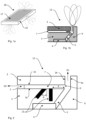
- Fig. 1a shows, very schematically, an electronic device 20 such as a mobile phone or a tablet.
- the electronic device 20 comprises a redirecting structure 12 for redirection of electromagnetic waves having a wavelength ⁇ , shown schematically in Fig. 1b and comprising at least one antenna structure.
- the electronic device 20 furthermore comprises a display 17 and a frame.
- the frame comprises a main frame section 18, extending essentially in parallel with the display 17, and a peripheral frame section 19 at least partially surrounding a peripheral edge of the display 17.
- the main frame section 18 may be e.g. a chassis or a printed circuit board (PCB), and the peripheral frame section 19 may a metal housing.
- the frame i.e.
- main frame section 18 and peripheral frame section 19, may be one integral component, or may be at least two separate components.
- At least one antenna structure extends between the display 17 and the peripheral frame section 19.
- the electronic device 20 may further comprise a mechanical structure 21, e.g. a camera, speaker, or sensor, arranged at least partially between the main frame section 18 and the display 17, and at least a part of the redirecting structure 12 may be arranged on the mechanical structure 21.
- the redirecting structure comprises at least a first reflection passage 1 formed between a first conductive surface 2a of a first conductive element 2 and a first conductive surface 3a of a second conductive element 3.
- the first conductive element 2 may be the display 17, and the second conductive element 3 may be the main frame section 18, in which embodiment the first reflection passage 1 extends between the display 17 and the main frame section 18.
- the redirecting structure 12 further comprises at least one antenna structure comprising at least one antenna element 4 and at least one radiation passage 5 extending from the antenna element 4 in a first direction D1, which may be a direction towards the first conductive element 2.
- Antenna element 4 is configured to emit electromagnetic waves, which electromagnetic waves propagate at least partially through the radiation passage 5.
- the description below refers to an antenna structure comprising a single antenna element 4, for ease of reading, however the antenna structure preferably comprises multiple antenna elements 4.
- the antenna structure is connected to the first reflection passage 1 at a first interface 6.
- the first reflection passage 1 extends in a second direction D2 which is different from the first direction D1.
- the first reflection passage 1 and the radiation passage 5 may be arranged at any angle in relation to each other.
- the redirecting structure 12 further comprises a first reflective structure 7 associated with an interior of the first reflection passage 1, allowing, e.g., the radiation to be directed to the display side of the electronic device 20 by using a proper propagation channel, such as waveguide.
- the first reflective structure 7 is arranged at a predetermined distance X from the first interface 6, such that electromagnetic waves propagating from the antenna structure into the first reflection passage 1 are reflected to the radiation passage 5 by the first reflective structure 7.
- the first reflective structure 7 extends in parallel with a longitudinal extension of the antenna element 4.
- the predetermined distance X is quarter wavelength ⁇ /4 ⁇ 25 %, which can reduce the amount of leaked radiation by 40 dB from 26 to 42 GHz.
- the redirecting structure 12 may comprise a second reflection passage 8 formed between a second conductive surface 3b of the second conductive element 3 and a first conductive surface 9a of a third conductive element 9, in which embodiment the second reflection passage 8 extends in a third direction D3.
- This allows placing the first reflective structure 7 under the first conductive element 2, which in one embodiment is display 17, in such a way that radiation from a potential radiation leak inside the display 17 is reflected.
- the antenna element 4 is placed on the second conductive element 3, which in one embodiment is the main frame section 18, adjacent but separated from the first reflective structure 7.
- the third direction D3 is different from the first direction D1 and the second direction D2.
- the first reflection passage 1, the radiation passage 5, and the second reflection passage 8 may be arranged at any angle in relation to each other.
- the antenna structure comprises a second interface 10 connecting the radiation passage 5 to the second reflection passage 8.
- the antenna element 4 may be placed just under the first conductive element 2/display 17. However, there may be a gap between antenna element 4 and the second conductive element 3/main frame section 18, and some radiation may leak in an unwanted direction.
- a further reflective structure 11 is preferably placed on a surface in the unwanted direction, e.g. the second conductive surface 3b.
- the first reflective structure 7 is placed on the second conductive element 3/main frame section 18 under the display, i.e. on the first conductive surface 3a.
- the antenna element 4 may be placed on the second conductive element 3/main frame section 18, preferably the second conductive surface 3b. Radiation may potentially leak from inside the first conductive element 2/display 17 or the back of the electronic device 20.
- the first reflective structure 7 is placed on the second conductive element 3/main frame section 18, under the first conductive element 2/display 17, and/or next to the third conductive element 9, which in one embodiment is peripheral frame section 19. With this kind of placement, unwanted radiation towards the back of the electronic device 20 can be minimized.
- the first reflection passage 1 and the second reflection passage 8 may be filled with one of air, dielectric, and a foam material.
- the third conductive element 9 may be the peripheral frame section 19, which is arranged to surround the periphery of the display 17 and the main frame section 18, in which embodiment the second reflection passage 8 extends between the main frame section 18 and the peripheral frame section 19.
- the redirecting structure 12 may comprise a second reflective structure 11 associated with an interior of the second reflection passage 8.
- the second reflective structure 11 is arranged at the predetermined distance X from the second interface 10, such that electromagnetic waves propagating from the antenna structure into the second reflection passage 8 are reflected to the radiation passage 5 by the second reflective structure 11.
- the second reflective structure 11 extends in parallel with a longitudinal extension of the antenna element 4.
- At least one of the first reflective structure 7 and the second reflective structure 11 may be arranged on the mechanical structure 21.
- the main frame section 18 and the peripheral frame section 19 may be separated by the second reflection passage 8, as shown in Figs. 4b to 4d , by the radiation passage 5 of the antenna structure, as shown in Fig. 4a , or by both.
- the first conductive element 2 may be the main frame section 18, and the second conductive element 3 may be the peripheral frame section 19, in which embodiment the first reflection passage 1 extends between the main frame section 18 and the peripheral frame section 19, as shown in Fig. 5 .
- the main frame section 18 and the peripheral frame section 19 are separated by the first reflection passage 1 and by the radiation passage 5 of the antenna structure.
- the first reflective structure 7 may be arranged at the first conductive surface 2a of the main frame section 18 and, optionally, the second reflective structure 11 may be arranged at a second conductive surface 2b of the main frame section 18.
- the electromagnetic waves may propagate in the first direction D1 within the radiation passage 5, in the second direction D2 within the first reflection passage 1, and/or in the third direction D3 within the second reflection passage 8.
- the radiation passage 5 extends from the antenna element 4 between the second conductive surface 2b of the first conductive element 2 and the second conductive surface 3b of the second conductive element 3. In a further embodiment, the radiation passage 5 extends between the second conductive surface 2b of the first conductive element 2 and the first conductive surface 9a of the third conductive element 9, as shown in Figs. 4a to 4d .
- the radiation passage 5 extends from the antenna element 4 and partially between the first conductive surface 2a of the first conductive element 2 and the first conductive surface 3a of the second conductive element 3.
- the first reflective structure 7 and the second reflective structure 11 are configured to optimize the amount of electromagnetic waves propagating in the first direction D1 by reflecting electromagnetic waves from at least one of the first reflection passage 7 and the second reflection passage 8 to the radiation passage 5, reducing the amount of electromagnetic waves propagating in the second direction D2 and the third direction D3.
- the first reflective structure 7 is arranged at the first conductive surface 3a of the second conductive element 3, as shown in Figs. 2 , Figs. 4a to 4d, and 5 .
- the second reflective structure 11 may be arranged at the second conductive surface 3b of the second conductive element 3, as shown in Fig. 4c , or may be arranged at the first surface 9a of the third conductive element 9.
- At least one of the first reflective structure 7 and the second reflective structure 11 comprise an artificial reflective electromagnetic surface, e.g. comprising metal.
- One, or both, of the first reflective structure 7 and the second reflective structure 11 may comprise at least one dielectric material, such as insert molding/nano injection molding plastics, ceramic materials, flexible materials, foams, polymers, and combinations.
- At least one of the first reflective structure 7 and the second reflective structure 11 has a longitudinal extension L being of the same length as, or longer than, the longitudinal extension of the antenna element 4.
- At least one of the first reflective structure 7 and the second reflective structure 11 may have a transverse extension being of a height equal to the predetermined distance X.
- At least one of the first reflective structure 7 and the second reflective structure 11 may comprise at least one groove 13, as shown in Figs. 2 , 4a to 4d , and 6 , or at least one row 14 of protrusions 14a, as shown in Figs. 5 and 6b .
- the longitudinal extension L of the groove 13 or row 14 of protrusions corresponds to the longitudinal extension of the antenna element 4.
- Each groove 13 extends into a body of the second conductive element 3, as shown in Figs. 2 and 4a to 4d , or into a body of the third conductive element 9.
- Each groove 13 may furthermore extend at an angle ⁇ > 0 ° to the first conductive surface 3a of the second conductive element 3, to the second conductive surface 3b of the second conductive element 3, or to the first conductive surface 9a of the third conductive element 9.
- Each groove 13 may comprise of a continuous recess, as shown in Fig. 6a , or of a plurality of individual cavities, the individual cavities being arranged in sequence in the direction of the longitudinal extension L of the groove 13.
- the continuous recess as well as the individual cavities may have any suitable shape such as that of a parallelepiped or a cylinder.
- Each row 14 of protrusions 14a extends from the first conductive surface 3a of the second conductive element 3, the second conductive surface 3b of the second conductive element 3, or the first conductive surface 9a of the third conductive element 9.
- Each protrusion 14a extends into the interior of the first reflection passage 1 or the interior of the second reflection passage 8.
- the row 14 of protrusions comprises at least one protrusion 14a, and each protrusion 14a may extend at, e.g., a 90° angle to the first conductive surface 3a of the second conductive element 3, to the second conductive surface 3b of the second conductive element 3, or to the first conductive surface 9a of the third conductive element 9.
- Each protrusion 14a of a row 14 of protrusions is arranged in sequence in the direction of the longitudinal extension L of the row of protrusions, as shown in Fig. 6b .
- the protrusions 14a may have any suitable shape such as that of a parallelepiped or a cylinder.
- At least one of the first reflective structure 7 and the second reflective structure 8 may comprise a plurality of grooves 13 or a plurality of rows 14 of protrusions, each groove 13 or protrusion 14a of the first reflective structure 7 and the second reflective structure 11 having the same transverse extension.
- at least two of the grooves 13 and the protrusions 14a comprises dielectric materials having different dielectric properties.
- the transverse extension is constant height for the first reflective structure 7 and the second reflective structure 8, and variable electrical lengths for the reflective structures 7, 8 are achieved by the different dielectric properties.
- Such a first reflective structure 7 and second reflective structure 8 can be made extremely wideband or to cover multiple frequency bands.
- each groove 13 or row 14 of protrusions comprising the same dielectric material, and at least two of the grooves 13 and the rows 14 of protrusions have different transverse extensions.
- the calculated physical height gives a proper height at one specific frequency.
- the desired operating range should be wide and may include, e.g., a frequency range from 26.5 GHz to 29.5 GHz.
- At least one of the first reflective structure 7 and the second reflective structure 11 may comprise a first reflective set 15 which comprises at least one groove 13 or at least one row 14 of protrusions.
- the longitudinal extension L1 of the first reflective set 15 is parallel with the longitudinal extension of the antenna element 4.
- the redirecting structure 12 may comprise a first antenna structure and a second antenna structure.
- Antenna element 4 of the second antenna structure has a longitudinal extension which is perpendicular to a longitudinal extension of the antenna element 4 of the first antenna structure.
- At least one of the first reflective structure 7 and the second reflective structure 11 comprises a second reflective set 16 which comprises at least one groove 13 or at least one row 14 of protrusions.
- the longitudinal extension L2 of the second reflective set 16 is perpendicular to the longitudinal extension L1 of the first reflective set 15, such that a groove 13 or row 14 of protrusions of the first reflective set 15 intersects a groove 13 or row 14 of protrusions of the second reflective set 16.
- the first reflective set 15 extends in parallel with the longitudinal extension L of the first antenna structure
- the second reflective set 16 extends in parallel with the longitudinal extension L of the second antenna structure.
- the redirecting structure 12 comprises a matrix of grooves 13 and/or rows 14 of protrusions, which is preferable when the antenna aperture is not properly defined.
- the reference signs used in the claims shall not be construed as limiting the scope. extends in a third direction D3. This allows placing the first reflective structure 7 under the first conductive element 2, which in one embodiment is display 17, in such a way that radiation from a potential radiation leak inside the display 17 is reflected.
- the antenna element 4 is placed on the second conductive element 3, which in one embodiment is the main frame section 18, adjacent but separated from the first reflective structure 7.
- the third direction D3 is different from the first direction D1 and the second direction D2.
- the first reflection passage 1, the radiation passage 5, and the second reflection passage 8 may be arranged at any angle in relation to each other.
- the antenna structure comprises a second interface 10 connecting the radiation passage 5 to the second reflection passage 8.
- the antenna element 4 may be placed just under the first conductive element 2/display 17. However, there may be a gap between antenna element 4 and the second conductive element 3/main frame section 18, and some radiation may leak in an unwanted direction.
- a further reflective structure 11 is preferably placed on a surface in the unwanted direction, e.g. the second conductive surface 3b.
- the first reflective structure 7 is placed on the second conductive element 3/main frame section 18 under the display, i.e. on the first conductive surface 3a.
- the antenna element 4 may be placed on the second conductive element 3/main frame section 18, preferably the second conductive surface 3b. Radiation may potentially leak from inside the first conductive element 2/display 17 or the back of the electronic device 20.
- the first reflective structure 7 is placed on the second conductive element 3/main frame section 18, under the first conductive element 2/display 17, and/or next to the third conductive element 9, which in one embodiment is peripheral frame section 19. With this kind of placement, unwanted radiation towards the back of the electronic device 20 can be minimized.
- the first reflection passage 1 and the second reflection passage 8 may be filled with one of air, dielectric, and a foam material.
- the third conductive element 9 may be the peripheral frame section 19, which is arranged to surround the periphery of the display 17 and the main frame section 18, in which embodiment the second reflection passage 8 extends between the main frame section 18 and the peripheral frame section 19.
- the redirecting structure 12 may comprise a second reflective structure 11 associated with an interior of the second reflection passage 8.
- the second reflective structure 11 is arranged at the predetermined distance X from the second interface 10, such that electromagnetic waves propagating from the antenna structure into the second reflection passage 8 are reflected to the radiation passage 5 by the second reflective structure 11.
- the second reflective structure 11 extends in parallel with a longitudinal extension of the antenna element 4.
- At least one of the first reflective structure 7 and the second reflective structure 11 may be arranged on the mechanical structure 21.
- the main frame section 18 and the peripheral frame section 19 may be separated by the second reflection passage 8, as shown in Figs. 4b to 4d , by the radiation passage 5 of the antenna structure, as shown in Fig. 4a , or by both.
- the first conductive element 2 may be the main frame section 18, and the second conductive element 3 may be the peripheral frame section 19, in which embodiment the first reflection passage 1 extends between the main frame section 18 and the peripheral frame section 19, as shown in Fig. 5 .
- the main frame section 18 and the peripheral frame section 19 are separated by the first reflection passage 1 and by the radiation passage 5 of the antenna structure.
- the first reflective structure 7 may be arranged at the first conductive surface 2a of the main frame section 18 and, optionally, the second reflective structure 11 may be arranged at a second conductive surface 2b of the main frame section 18.
- the electromagnetic waves may propagate in the first direction D1 within the radiation passage 5, in the second direction D2 within the first reflection passage 1, and/or in the third direction D3 within the second reflection passage 8.
- the radiation passage 5 extends from the antenna element 4 between the second conductive surface 2b of the first conductive element 2 and the second conductive surface 3b of the second conductive element 3. In a further embodiment, the radiation passage 5 extends between the second conductive surface 2b of the first conductive element 2 and the first conductive surface 9a of the third conductive element 9, as shown in Figs. 4a to 4d .
- the radiation passage 5 extends from the antenna element 4 and partially between the first conductive surface 2a of the first conductive element 2 and the first conductive surface 3a of the second conductive element 3.
- the first reflective structure 7 and the second reflective structure 11 are configured to optimize the amount of electromagnetic waves propagating in the first direction D1 by reflecting electromagnetic waves from at least one of the first reflection passage 7 and the second reflection passage 8 to the radiation passage 5, reducing the amount of electromagnetic waves propagating in the second direction D2 and the third direction D3.
- the first reflective structure 7 is arranged at the first conductive surface 3a of the second conductive element 3, as shown in Figs. 2 , 4a to 4d, and 5 .
- the second reflective structure 11 may be arranged at the second conductive surface 3b of the second conductive element 3, as shown in Fig. 4c , or may be arranged at the first surface 9a of the third conductive element 9.
- At least one of the first reflective structure 7 and the second reflective structure 11 comprise an artificial reflective electromagnetic surface, e.g. comprising metal.
- One, or both, of the first reflective structure 7 and the second reflective structure 11 may comprise at least one dielectric material, such as insert molding/nano injection molding plastics, ceramic materials, flexible materials, foams, polymers, and combinations.
- At least one of the first reflective structure 7 and the second reflective structure 11 has a longitudinal extension L being of the same length as, or longer than, the longitudinal extension of the antenna element 4.
- At least one of the first reflective structure 7 and the second reflective structure 11 may have a transverse extension being of a height equal to the predetermined distance X.
- At least one of the first reflective structure 7 and the second reflective structure 11 may comprise at least one groove 13, as shown in Figs. 2 , 4a to 4d , and 6 , or at least one row 14 of protrusions 14a, as shown in Figs. 5 and 6b .
- the longitudinal extension L of the groove 13 or row 14 of protrusions corresponds to the longitudinal extension of the antenna element 4.
- Each groove 13 extends into a body of the second conductive element 3, as shown in Figs. 2 and 4a to 4d , or into a body of the third conductive element 9.
- Each groove 13 may furthermore extend at an angle ⁇ > 0° to the first conductive surface 3a of the second conductive element 3, to the second conductive surface 3b of the second conductive element 3, or to the first conductive surface 9a of the third conductive element 9.
- Each groove 13 may comprise of a continuous recess, as shown in Fig. 6a , or of a plurality of individual cavities, the individual cavities being arranged in sequence in the direction of the longitudinal extension L of the groove 13.
- the continuous recess as well as the individual cavities may have any suitable shape such as that of a parallelepiped or a cylinder.
- Each row 14 of protrusions 14a extends from the first conductive surface 3a of the second conductive element 3, the second conductive surface 3b of the second conductive element 3, or the first conductive surface 9a of the third conductive element 9.
- Each protrusion 14a extends into the interior of the first reflection passage 1 or the interior of the second reflection passage 8.
- the row 14 of protrusions comprises at least one protrusion 14a, and each protrusion 14a may extend at, e.g., a 90° angle to the first conductive surface 3a of the second conductive element 3, to the second conductive surface 3b of the second conductive element 3, or to the first conductive surface 9a of the third conductive element 9.
- Each protrusion 14a of a row 14 of protrusions is arranged in sequence in the direction of the longitudinal extension L of the row of protrusions, as shown in Fig. 6b .
- the protrusions 14a may have any suitable shape such as that of a parallelepiped or a cylinder.
- At least one of the first reflective structure 7 and the second reflective structure 8 may comprise a plurality of grooves 13 or a plurality of rows 14 of protrusions, each groove 13 or protrusion 14a of the first reflective structure 7 and the second reflective structure 11 having the same transverse extension.
- at least two of the grooves 13 and the protrusions 14a comprises dielectric materials having different dielectric properties.
- the transverse extension is constant height for the first reflective structure 7 and the second reflective structure 8, and variable electrical lengths for the reflective structures 7, 8 are achieved by the different dielectric properties.
- Such a first reflective structure 7 and second reflective structure 8 can be made extremely wideband or to cover multiple frequency bands.
- each groove 13 or row 14 of protrusions comprising the same dielectric material, and at least two of the grooves 13 and the rows 14 of protrusions have different transverse extensions.
- the calculated physical height gives a proper height at one specific frequency.
- the desired operating range should be wide and may include, e.g., a frequency range from 26.5 GHz to 29.5 GHz.
- the reflective structure 7, 11 is designed to operate at low band (26.5 - 29.5 GHz)
- At least one of the first reflective structure 7 and the second reflective structure 11 may comprise a first reflective set 15 which comprises at least one groove 13 or at least one row 14 of protrusions.
- the longitudinal extension L1 of the first reflective set 15 is parallel with the longitudinal extension of the antenna element 4.
- the redirecting structure 12 may comprise a first antenna structure and a second antenna structure.
- Antenna element 4 of the second antenna structure has a longitudinal extension which is perpendicular to a longitudinal extension of the antenna element 4 of the first antenna structure.
- At least one of the first reflective structure 7 and the second reflective structure 11 comprises a second reflective set 16 which comprises at least one groove 13 or at least one row 14 of protrusions.
- the longitudinal extension L2 of the second reflective set 16 is perpendicular to the longitudinal extension L1 of the first reflective set 15, such that a groove 13 or row 14 of protrusions of the first reflective set 15 intersects a groove 13 or row 14 of protrusions of the second reflective set 16.
- the first reflective set 15 extends in parallel with the longitudinal extension L of the first antenna structure
- the second reflective set 16 extends in parallel with the longitudinal extension L of the second antenna structure.
- the redirecting structure 12 comprises a matrix of grooves 13 and/or rows 14 of protrusions, which is preferable when the antenna aperture is not properly defined.
Landscapes
- Engineering & Computer Science (AREA)
- Computer Networks & Wireless Communication (AREA)
- Aerials With Secondary Devices (AREA)
Claims (14)
- Dispositif électronique (20) comprenant une structure de redirection (12) d'ondes électromagnétiques ayant une longueur d'onde (λ), la structure de redirection comprenant :un premier passage de réflexion (1) formé entre une première surface conductrice (2a) d'un premier élément conducteur (2) et une première surface conductrice (3a) d'un deuxième élément conducteur (3),au moins une structure d'antenne comprenant au moins un élément d'antenne (4) et au moins un passage de rayonnement (5) s'étendant depuis ledit élément d'antenne (4) dans une première direction (D1),ledit élément d'antenne (4) étant configuré pour émettre des ondes électromagnétiques, lesdites ondes électromagnétiques étant configurées pour se propager au moins partiellement à travers ledit passage de rayonnement (5),ladite structure d'antenne étant connectée audit premier passage de réflexion (1) au niveau d'une première interface (6), ledit premier passage de réflexion (1) s'étendant dans une deuxième direction (D2), ladite deuxième direction (D2) étant différente de ladite première direction (D1),une première structure réfléchissante (7) associée à un intérieur dudit premier passage de réflexion (1),ladite première structure réfléchissante (7) étant agencée à une distance prédéterminée (X) de ladite première interface (6), de sorte que les ondes électromagnétiques se propageant depuis ladite structure d'antenne dans ledit premier passage de réflexion (1) sont réfléchies vers ledit passage de rayonnement (5) par ladite première structure réfléchissante (7),ladite première structure réfléchissante (7) s'étendant parallèlement à une extension longitudinale dudit élément d'antenne (4), ledit dispositif électronique (20) comprenant en outre :un afficheur (17) et une armature, ladite armature comprenant une section d'armature principale (18), s'étendant essentiellement parallèlement audit afficheur (17), et une section d'armature périphérique (19) entourant au moins partiellement un bord périphérique dudit afficheur (17), etle passage de rayonnement (5) s'étend jusqu'à une seconde structure d'antenne s'étendant au moins entre ledit afficheur (17) et ladite section d'armature périphérique (19).
- Dispositif électronique (20) selon la revendication 1, dans lequel ladite structure de redirection (12) comprend en outre un second passage de réflexion (8) formé entre une seconde surface conductrice (3b) dudit deuxième élément conducteur (3) et une première surface conductrice (9a) d'un troisième élément conducteur (9), ledit second passage de réflexion (8) s'étendant dans une troisième direction (D3), ladite troisième direction (D3) étant différente de ladite première direction (D1) et de ladite deuxième direction (D2),
ladite structure d'antenne comprenant une seconde interface (10) connectant ledit passage de rayonnement (5) audit second passage de réflexion (8). - Dispositif électronique (20) selon la revendication 2, dans lequel ladite structure de redirection (12) comprend en outre une seconde structure réfléchissante (11) associée à un intérieur dudit second passage de réflexion (8), ladite seconde structure réfléchissante (11) étant agencé à ladite distance prédéterminée (X) de ladite seconde interface (10), de sorte que les ondes électromagnétiques se propageant depuis ladite structure d'antenne dans ledit second passage de réflexion (8) sont réfléchies vers ledit passage de rayonnement (5) par ladite seconde structure réfléchissante (11),
ladite seconde structure réfléchissante (11) s'étendant parallèlement à une extension longitudinale dudit élément d'antenne (4). - Dispositif électronique (20) selon l'une quelconque des revendications précédentes, dans lequel ledit passage de rayonnement (5) s'étend depuis ledit élément d'antenne (4) dans une direction vers ledit premier élément conducteur (2).
- Dispositif électronique (20) selon l'une quelconque des revendications 2 à 4, dans lequel ledit passage de rayonnement (5) s'étend depuis ledit élément d'antenne (4) entre une seconde surface conductrice (2b) dudit premier élément conducteur (2) et une seconde surface conductrice (3b) dudit deuxième élément conducteur (3) ou entre ladite seconde surface conductrice dudit premier élément conducteur (2b) et ladite première surface conductrice (9a) dudit troisième élément conducteur (9).
- Dispositif électronique (20) selon l'une quelconque des revendications 3 à 5, dans lequel ladite première structure réfléchissante (7) est agencée au niveau de ladite première surface conductrice (3a) dudit deuxième élément conducteur (3) et/ou ladite seconde structure réfléchissante (11) est agencée au niveau de ladite seconde surface conductrice (3b) dudit deuxième élément conducteur (3) ou de ladite première surface conductrice (9a) dudit troisième élément conducteur (9).
- Dispositif électronique (20) selon l'une quelconque des revendications 3 à 6, dans lequel au moins l'une de ladite première structure réfléchissante (7) et de ladite seconde structure réfléchissante (11) a une extension longitudinale (L) étant de longueur égale, ou supérieure à ladite extension longitudinale dudit élément d'antenne (4).
- Dispositif électronique (20) selon la revendication 7, dans lequel au moins une parmi ladite première structure réfléchissante (7) et ladite seconde structure réfléchissante (11) a une extension transversale étant d'une hauteur égale à ladite distance prédéterminée (X).
- Dispositif électronique (20) selon l'une quelconque des revendications 3 à 8, dans lequel au moins l'une de ladite première structure réfléchissante (7) et de ladite seconde structure réfléchissante (11) comprend au moins un matériau diélectrique.
- Dispositif électronique (20) selon la revendication 2 ou l'une quelconque des revendications 3 à 9 lorsqu'elles dépendent de la revendication 2, dans lequel au moins l'un dudit premier passage de réflexion (1) et dudit second passage de réflexion (8) est rempli d'un élément parmi l'air, le vide et un matériau en mousse.
- Dispositif électronique (20) selon l'une quelconque des revendications précédentes, dans lequel ladite distance prédéterminée (X) est un quart de longueur d'onde (λ/4)± 25 %.
- Dispositif électronique (20) selon l'une quelconque des revendications précédentes, dans lequel ledit afficheur (17) est le premier élément conducteur (2), ladite section d'armature principale (18) est le deuxième élément conducteur (3), et le premier passage de réflexion (1) s'étend entre ledit afficheur (17) et ladite section d'armature principale (18), dans lequel ladite section d'armature principale (18) et ladite section d'armature périphérique (19) sont séparées au moyen d'au moins l'un d'un second passage de réflexion (8) et le passage de rayonnement (5) de ladite structure d'antenne.
- Dispositif électronique (20) selon la revendication 12, dans lequel ladite section d'armature périphérique (19) est un troisième élément conducteur (9) entourant la périphérie dudit afficheur (17) et ladite section d'armature principale (18), ledit second passage de réflexion (8) s'étendant entre ladite section d'armature principale (18) et ladite section d'armature périphérique (19).
- Dispositif électronique (20) selon l'une quelconque des revendications 1 à 11, dans lequel ladite section d'armature principale (18) est le premier élément conducteur (2), ladite section d'armature périphérique (19) est le deuxième élément conducteur (3), et le premier passage de réflexion (1) s'étend entre ladite section d'armature principale (18) et ladite section d'armature périphérique (19), ladite section d'armature principale (18) et ladite section d'armature périphérique (19) étant séparées au moyen dudit premier passage de réflexion (1) et le passage de rayonnement (5) de ladite structure d'antenne.
Applications Claiming Priority (1)
| Application Number | Priority Date | Filing Date | Title |
|---|---|---|---|
| PCT/EP2019/056400 WO2020182311A1 (fr) | 2019-03-14 | 2019-03-14 | Structure de redirection d'ondes électromagnétiques |
Publications (2)
| Publication Number | Publication Date |
|---|---|
| EP3918664A1 EP3918664A1 (fr) | 2021-12-08 |
| EP3918664B1 true EP3918664B1 (fr) | 2023-10-11 |
Family
ID=65904375
Family Applications (1)
| Application Number | Title | Priority Date | Filing Date |
|---|---|---|---|
| EP19712924.0A Active EP3918664B1 (fr) | 2019-03-14 | 2019-03-14 | Structure de redirection d'ondes électromagnétiques |
Country Status (4)
| Country | Link |
|---|---|
| US (1) | US11955711B2 (fr) |
| EP (1) | EP3918664B1 (fr) |
| CN (1) | CN113424364B (fr) |
| WO (1) | WO2020182311A1 (fr) |
Families Citing this family (2)
| Publication number | Priority date | Publication date | Assignee | Title |
|---|---|---|---|---|
| EP4238177A1 (fr) * | 2020-12-21 | 2023-09-06 | Huawei Technologies Co., Ltd. | Feuille thermoconductrice, son procédé d'installation et son procédé de fabrication |
| EP4302361A1 (fr) * | 2021-03-26 | 2024-01-10 | Huawei Technologies Co., Ltd. | Agencement de direction de faisceau pour appareil électronique |
Citations (1)
| Publication number | Priority date | Publication date | Assignee | Title |
|---|---|---|---|---|
| US9972892B2 (en) * | 2016-04-26 | 2018-05-15 | Apple Inc. | Electronic device with millimeter wave antennas on stacked printed circuits |
Family Cites Families (28)
| Publication number | Priority date | Publication date | Assignee | Title |
|---|---|---|---|---|
| JP3470184B2 (ja) * | 2000-04-28 | 2003-11-25 | 福井県 | 平面アンテナ |
| JP4203404B2 (ja) * | 2003-11-26 | 2009-01-07 | 京セラ株式会社 | 導波管構造体の分岐構造およびアンテナ基板 |
| US7623073B2 (en) | 2005-11-14 | 2009-11-24 | Anritsu Corporation | Linearly polarized antenna and radar apparatus using the same |
| JP2007166115A (ja) * | 2005-12-12 | 2007-06-28 | Matsushita Electric Ind Co Ltd | アンテナ装置 |
| US7804453B2 (en) * | 2008-04-16 | 2010-09-28 | Apple Inc. | Antennas for wireless electronic devices |
| WO2010003808A2 (fr) * | 2008-07-07 | 2010-01-14 | Kildal Antenna Consulting Ab | Guide d’ondes et lignes de transmission dans des interstices entre des surfaces conductrices parallèles |
| JP5334242B2 (ja) * | 2008-09-05 | 2013-11-06 | 大学共同利用機関法人自然科学研究機構 | 受信イメージングアンテナアレイ |
| EP2343774A4 (fr) * | 2008-10-29 | 2013-11-27 | Panasonic Corp | Guide d' onde haute fréquence et déphaseur l utilisant, radiateur, dispositif électronique qui utilise ce déphaseur et ce radiateur, dispositif d' antenne et dispositif électronique équipé de celui-ci |
| CN102315517B (zh) * | 2010-06-29 | 2014-04-16 | 华为技术有限公司 | 一种定向天线设备、多输入多输出传输定向天线设备 |
| CN102044752B (zh) | 2010-12-07 | 2013-10-23 | 惠州Tcl移动通信有限公司 | 带u字型高阻抗表面金属条接地的天线及其无线通讯装置 |
| CN102044753B (zh) | 2010-12-07 | 2013-10-02 | 惠州Tcl移动通信有限公司 | 带十字型高阻抗表面金属条接地的天线及其无线通讯装置 |
| JP5959368B2 (ja) * | 2012-08-27 | 2016-08-02 | 日本無線株式会社 | レーダアンテナ |
| TW201433004A (zh) * | 2013-02-08 | 2014-08-16 | Sj Antenna Design | 天線反射裝置 |
| JP2014165997A (ja) * | 2013-02-22 | 2014-09-08 | Toshiba Corp | 電磁波漏洩防止装置および無線電力伝送システム |
| EP2772985B1 (fr) * | 2013-02-27 | 2018-08-08 | Alcatel-Lucent Shanghai Bell Co., Ltd | Système de fixation d'un radôme plan sur le réflecteur concave d'une antenne |
| CN104064844B (zh) * | 2013-03-19 | 2019-03-15 | 德克萨斯仪器股份有限公司 | 可缩回的介电波导 |
| TWI559613B (zh) * | 2015-09-22 | 2016-11-21 | 智易科技股份有限公司 | 高隔離度之多天線結構 |
| DE112016000180B4 (de) * | 2015-11-05 | 2023-08-03 | Nidec Corporation | Schlitz-Array-Antenne |
| DE102017102284A1 (de) * | 2016-02-08 | 2017-08-10 | Nidec Elesys Corporation | Wellenleitervorrichtung und Antennenvorrichtung mit der Wellenleitervorrichtung |
| CN208955165U (zh) * | 2016-06-29 | 2019-06-07 | 日本电产株式会社 | 雷达装置 |
| US10490907B2 (en) | 2016-09-27 | 2019-11-26 | Google Llc | Suppression of surface waves in printed circuit board-based phased-array antennas |
| JP7020677B2 (ja) * | 2017-04-13 | 2022-02-16 | 日本電産エレシス株式会社 | スロットアンテナ装置 |
| CN208093762U (zh) * | 2017-04-14 | 2018-11-13 | 日本电产株式会社 | 缝隙天线装置以及雷达装置 |
| JP2020520180A (ja) * | 2017-05-11 | 2020-07-02 | 日本電産株式会社 | 導波路装置および当該導波路装置を備えるアンテナ装置 |
| CN108987866A (zh) * | 2017-06-05 | 2018-12-11 | 日本电产株式会社 | 波导装置以及具有该波导装置的天线装置 |
| US20180375185A1 (en) * | 2017-06-26 | 2018-12-27 | WGR Co., Ltd. | Electromagnetic wave transmission device |
| CN107404000B (zh) * | 2017-07-14 | 2020-03-31 | 南京邮电大学 | 一种糖铲型扇形波束水平扫描天线 |
| JP2019050568A (ja) * | 2017-09-07 | 2019-03-28 | 日本電産株式会社 | 方向性結合器 |
-
2019
- 2019-03-14 CN CN201980091945.XA patent/CN113424364B/zh active Active
- 2019-03-14 WO PCT/EP2019/056400 patent/WO2020182311A1/fr unknown
- 2019-03-14 US US17/438,015 patent/US11955711B2/en active Active
- 2019-03-14 EP EP19712924.0A patent/EP3918664B1/fr active Active
Patent Citations (1)
| Publication number | Priority date | Publication date | Assignee | Title |
|---|---|---|---|---|
| US9972892B2 (en) * | 2016-04-26 | 2018-05-15 | Apple Inc. | Electronic device with millimeter wave antennas on stacked printed circuits |
Also Published As
| Publication number | Publication date |
|---|---|
| US11955711B2 (en) | 2024-04-09 |
| EP3918664A1 (fr) | 2021-12-08 |
| CN113424364A (zh) | 2021-09-21 |
| US20220149531A1 (en) | 2022-05-12 |
| WO2020182311A1 (fr) | 2020-09-17 |
| CN113424364B (zh) | 2023-05-09 |
Similar Documents
| Publication | Publication Date | Title |
|---|---|---|
| US11837787B2 (en) | High frequency filter and phased array antenna comprising such a high frequency filter | |
| US9698487B2 (en) | Array antenna | |
| EP1547201B1 (fr) | Reseau d'antennes a large bande a profil bas | |
| KR100621335B1 (ko) | 폴더타입 통신 핸드셋 장치 내에서의 접지효과 감소 장치 | |
| KR20210125019A (ko) | 하나 또는 그 이상의 메타물질 구조에 기초하는 안테나 어레이 | |
| EP2562872B1 (fr) | Dispositif dýantenne | |
| JP2010130095A (ja) | アンテナ装置および無線通信装置 | |
| CA3096346C (fr) | Appareil d'antenne reseau et dispositif de communication | |
| EP3918664B1 (fr) | Structure de redirection d'ondes électromagnétiques | |
| CN112397898A (zh) | 天线阵列组件及电子设备 | |
| JP2001326506A (ja) | アレイアンテナ | |
| US7598912B2 (en) | Planar antenna structure | |
| KR20080059012A (ko) | 안테나 장치 | |
| CN112889183B (zh) | 波束控制天线结构和包括所述结构的电子设备 | |
| KR20180052071A (ko) | 파라볼릭-하이퍼볼릭 반사기를 포함하는 안테나 장치 | |
| JP4713367B2 (ja) | 開口面アンテナ | |
| CN116195127A (zh) | 喇叭天线 | |
| JP4231457B2 (ja) | 誘電体アンテナ | |
| JP6474634B2 (ja) | 平面アレーアンテナ | |
| CN114221108B (zh) | 传输装置 | |
| CN112467389B (zh) | 电子设备 | |
| RU2488925C1 (ru) | Сверхширокополосная антенна | |
| JP6313813B2 (ja) | 給電装置 | |
| CN117458168A (zh) | 全息天线与通信设备 |
Legal Events
| Date | Code | Title | Description |
|---|---|---|---|
| STAA | Information on the status of an ep patent application or granted ep patent |
Free format text: STATUS: UNKNOWN |
|
| STAA | Information on the status of an ep patent application or granted ep patent |
Free format text: STATUS: THE INTERNATIONAL PUBLICATION HAS BEEN MADE |
|
| PUAI | Public reference made under article 153(3) epc to a published international application that has entered the european phase |
Free format text: ORIGINAL CODE: 0009012 |
|
| STAA | Information on the status of an ep patent application or granted ep patent |
Free format text: STATUS: REQUEST FOR EXAMINATION WAS MADE |
|
| 17P | Request for examination filed |
Effective date: 20210830 |
|
| AK | Designated contracting states |
Kind code of ref document: A1 Designated state(s): AL AT BE BG CH CY CZ DE DK EE ES FI FR GB GR HR HU IE IS IT LI LT LU LV MC MK MT NL NO PL PT RO RS SE SI SK SM TR |
|
| DAV | Request for validation of the european patent (deleted) | ||
| DAX | Request for extension of the european patent (deleted) | ||
| GRAP | Despatch of communication of intention to grant a patent |
Free format text: ORIGINAL CODE: EPIDOSNIGR1 |
|
| STAA | Information on the status of an ep patent application or granted ep patent |
Free format text: STATUS: GRANT OF PATENT IS INTENDED |
|
| RIC1 | Information provided on ipc code assigned before grant |
Ipc: H01P 1/04 20060101ALN20230412BHEP Ipc: H01P 5/19 20060101ALI20230412BHEP Ipc: H01Q 1/52 20060101ALI20230412BHEP Ipc: H01Q 13/06 20060101ALI20230412BHEP Ipc: H01Q 1/24 20060101AFI20230412BHEP |
|
| RIC1 | Information provided on ipc code assigned before grant |
Ipc: H01P 1/04 20060101ALN20230424BHEP Ipc: H01P 5/19 20060101ALI20230424BHEP Ipc: H01Q 1/52 20060101ALI20230424BHEP Ipc: H01Q 13/06 20060101ALI20230424BHEP Ipc: H01Q 1/24 20060101AFI20230424BHEP |
|
| INTG | Intention to grant announced |
Effective date: 20230510 |
|
| GRAS | Grant fee paid |
Free format text: ORIGINAL CODE: EPIDOSNIGR3 |
|
| P01 | Opt-out of the competence of the unified patent court (upc) registered |
Effective date: 20230727 |
|
| GRAA | (expected) grant |
Free format text: ORIGINAL CODE: 0009210 |
|
| STAA | Information on the status of an ep patent application or granted ep patent |
Free format text: STATUS: THE PATENT HAS BEEN GRANTED |
|
| AK | Designated contracting states |
Kind code of ref document: B1 Designated state(s): AL AT BE BG CH CY CZ DE DK EE ES FI FR GB GR HR HU IE IS IT LI LT LU LV MC MK MT NL NO PL PT RO RS SE SI SK SM TR |
|
| REG | Reference to a national code |
Ref country code: GB Ref legal event code: FG4D |
|
| REG | Reference to a national code |
Ref country code: CH Ref legal event code: EP |
|
| REG | Reference to a national code |
Ref country code: DE Ref legal event code: R096 Ref document number: 602019039096 Country of ref document: DE |
|
| REG | Reference to a national code |
Ref country code: IE Ref legal event code: FG4D |
|
| REG | Reference to a national code |
Ref country code: LT Ref legal event code: MG9D |
|
| REG | Reference to a national code |
Ref country code: NL Ref legal event code: MP Effective date: 20231011 |
|
| REG | Reference to a national code |
Ref country code: AT Ref legal event code: MK05 Ref document number: 1621166 Country of ref document: AT Kind code of ref document: T Effective date: 20231011 |
|
| PG25 | Lapsed in a contracting state [announced via postgrant information from national office to epo] |
Ref country code: NL Free format text: LAPSE BECAUSE OF FAILURE TO SUBMIT A TRANSLATION OF THE DESCRIPTION OR TO PAY THE FEE WITHIN THE PRESCRIBED TIME-LIMIT Effective date: 20231011 |
|
| PG25 | Lapsed in a contracting state [announced via postgrant information from national office to epo] |
Ref country code: GR Free format text: LAPSE BECAUSE OF FAILURE TO SUBMIT A TRANSLATION OF THE DESCRIPTION OR TO PAY THE FEE WITHIN THE PRESCRIBED TIME-LIMIT Effective date: 20240112 |
|
| PG25 | Lapsed in a contracting state [announced via postgrant information from national office to epo] |
Ref country code: IS Free format text: LAPSE BECAUSE OF FAILURE TO SUBMIT A TRANSLATION OF THE DESCRIPTION OR TO PAY THE FEE WITHIN THE PRESCRIBED TIME-LIMIT Effective date: 20240211 |
|
| PG25 | Lapsed in a contracting state [announced via postgrant information from national office to epo] |
Ref country code: LT Free format text: LAPSE BECAUSE OF FAILURE TO SUBMIT A TRANSLATION OF THE DESCRIPTION OR TO PAY THE FEE WITHIN THE PRESCRIBED TIME-LIMIT Effective date: 20231011 |
|
| PG25 | Lapsed in a contracting state [announced via postgrant information from national office to epo] |
Ref country code: AT Free format text: LAPSE BECAUSE OF FAILURE TO SUBMIT A TRANSLATION OF THE DESCRIPTION OR TO PAY THE FEE WITHIN THE PRESCRIBED TIME-LIMIT Effective date: 20231011 |
|
| PG25 | Lapsed in a contracting state [announced via postgrant information from national office to epo] |
Ref country code: ES Free format text: LAPSE BECAUSE OF FAILURE TO SUBMIT A TRANSLATION OF THE DESCRIPTION OR TO PAY THE FEE WITHIN THE PRESCRIBED TIME-LIMIT Effective date: 20231011 |
|
| PG25 | Lapsed in a contracting state [announced via postgrant information from national office to epo] |
Ref country code: LT Free format text: LAPSE BECAUSE OF FAILURE TO SUBMIT A TRANSLATION OF THE DESCRIPTION OR TO PAY THE FEE WITHIN THE PRESCRIBED TIME-LIMIT Effective date: 20231011 Ref country code: IS Free format text: LAPSE BECAUSE OF FAILURE TO SUBMIT A TRANSLATION OF THE DESCRIPTION OR TO PAY THE FEE WITHIN THE PRESCRIBED TIME-LIMIT Effective date: 20240211 Ref country code: GR Free format text: LAPSE BECAUSE OF FAILURE TO SUBMIT A TRANSLATION OF THE DESCRIPTION OR TO PAY THE FEE WITHIN THE PRESCRIBED TIME-LIMIT Effective date: 20240112 Ref country code: ES Free format text: LAPSE BECAUSE OF FAILURE TO SUBMIT A TRANSLATION OF THE DESCRIPTION OR TO PAY THE FEE WITHIN THE PRESCRIBED TIME-LIMIT Effective date: 20231011 Ref country code: BG Free format text: LAPSE BECAUSE OF FAILURE TO SUBMIT A TRANSLATION OF THE DESCRIPTION OR TO PAY THE FEE WITHIN THE PRESCRIBED TIME-LIMIT Effective date: 20240111 Ref country code: AT Free format text: LAPSE BECAUSE OF FAILURE TO SUBMIT A TRANSLATION OF THE DESCRIPTION OR TO PAY THE FEE WITHIN THE PRESCRIBED TIME-LIMIT Effective date: 20231011 Ref country code: PT Free format text: LAPSE BECAUSE OF FAILURE TO SUBMIT A TRANSLATION OF THE DESCRIPTION OR TO PAY THE FEE WITHIN THE PRESCRIBED TIME-LIMIT Effective date: 20240212 |
|
| PGFP | Annual fee paid to national office [announced via postgrant information from national office to epo] |
Ref country code: DE Payment date: 20240130 Year of fee payment: 6 Ref country code: GB Payment date: 20240201 Year of fee payment: 6 |