EP3916131A1 - Cobalt-tungsten alloy and method of fabricating the same - Google Patents
Cobalt-tungsten alloy and method of fabricating the same Download PDFInfo
- Publication number
- EP3916131A1 EP3916131A1 EP20193449.4A EP20193449A EP3916131A1 EP 3916131 A1 EP3916131 A1 EP 3916131A1 EP 20193449 A EP20193449 A EP 20193449A EP 3916131 A1 EP3916131 A1 EP 3916131A1
- Authority
- EP
- European Patent Office
- Prior art keywords
- cobalt
- tungsten
- alloy nanowires
- tungsten alloy
- content
- Prior art date
- Legal status (The legal status is an assumption and is not a legal conclusion. Google has not performed a legal analysis and makes no representation as to the accuracy of the status listed.)
- Pending
Links
Images





Classifications
-
- C—CHEMISTRY; METALLURGY
- C25—ELECTROLYTIC OR ELECTROPHORETIC PROCESSES; APPARATUS THEREFOR
- C25D—PROCESSES FOR THE ELECTROLYTIC OR ELECTROPHORETIC PRODUCTION OF COATINGS; ELECTROFORMING; APPARATUS THEREFOR
- C25D1/00—Electroforming
- C25D1/006—Nanostructures, e.g. using aluminium anodic oxidation templates [AAO]
-
- B—PERFORMING OPERATIONS; TRANSPORTING
- B22—CASTING; POWDER METALLURGY
- B22F—WORKING METALLIC POWDER; MANUFACTURE OF ARTICLES FROM METALLIC POWDER; MAKING METALLIC POWDER; APPARATUS OR DEVICES SPECIALLY ADAPTED FOR METALLIC POWDER
- B22F1/00—Metallic powder; Treatment of metallic powder, e.g. to facilitate working or to improve properties
- B22F1/07—Metallic powder characterised by particles having a nanoscale microstructure
-
- B—PERFORMING OPERATIONS; TRANSPORTING
- B22—CASTING; POWDER METALLURGY
- B22F—WORKING METALLIC POWDER; MANUFACTURE OF ARTICLES FROM METALLIC POWDER; MAKING METALLIC POWDER; APPARATUS OR DEVICES SPECIALLY ADAPTED FOR METALLIC POWDER
- B22F1/00—Metallic powder; Treatment of metallic powder, e.g. to facilitate working or to improve properties
- B22F1/14—Treatment of metallic powder
- B22F1/142—Thermal or thermo-mechanical treatment
-
- C—CHEMISTRY; METALLURGY
- C22—METALLURGY; FERROUS OR NON-FERROUS ALLOYS; TREATMENT OF ALLOYS OR NON-FERROUS METALS
- C22C—ALLOYS
- C22C19/00—Alloys based on nickel or cobalt
- C22C19/07—Alloys based on nickel or cobalt based on cobalt
-
- C—CHEMISTRY; METALLURGY
- C25—ELECTROLYTIC OR ELECTROPHORETIC PROCESSES; APPARATUS THEREFOR
- C25D—PROCESSES FOR THE ELECTROLYTIC OR ELECTROPHORETIC PRODUCTION OF COATINGS; ELECTROFORMING; APPARATUS THEREFOR
- C25D1/00—Electroforming
- C25D1/04—Wires; Strips; Foils
-
- C—CHEMISTRY; METALLURGY
- C25—ELECTROLYTIC OR ELECTROPHORETIC PROCESSES; APPARATUS THEREFOR
- C25D—PROCESSES FOR THE ELECTROLYTIC OR ELECTROPHORETIC PRODUCTION OF COATINGS; ELECTROFORMING; APPARATUS THEREFOR
- C25D3/00—Electroplating: Baths therefor
- C25D3/02—Electroplating: Baths therefor from solutions
- C25D3/56—Electroplating: Baths therefor from solutions of alloys
- C25D3/562—Electroplating: Baths therefor from solutions of alloys containing more than 50% by weight of iron or nickel or cobalt
-
- C—CHEMISTRY; METALLURGY
- C25—ELECTROLYTIC OR ELECTROPHORETIC PROCESSES; APPARATUS THEREFOR
- C25D—PROCESSES FOR THE ELECTROLYTIC OR ELECTROPHORETIC PRODUCTION OF COATINGS; ELECTROFORMING; APPARATUS THEREFOR
- C25D5/00—Electroplating characterised by the process; Pretreatment or after-treatment of workpieces
- C25D5/48—After-treatment of electroplated surfaces
- C25D5/50—After-treatment of electroplated surfaces by heat-treatment
-
- H—ELECTRICITY
- H10—SEMICONDUCTOR DEVICES; ELECTRIC SOLID-STATE DEVICES NOT OTHERWISE PROVIDED FOR
- H10P—GENERIC PROCESSES OR APPARATUS FOR THE MANUFACTURE OR TREATMENT OF DEVICES COVERED BY CLASS H10
- H10P14/00—Formation of materials, e.g. in the shape of layers or pillars
- H10P14/40—Formation of materials, e.g. in the shape of layers or pillars of conductive or resistive materials
- H10P14/46—Formation of materials, e.g. in the shape of layers or pillars of conductive or resistive materials using a liquid
-
- H—ELECTRICITY
- H10—SEMICONDUCTOR DEVICES; ELECTRIC SOLID-STATE DEVICES NOT OTHERWISE PROVIDED FOR
- H10W—GENERIC PACKAGES, INTERCONNECTIONS, CONNECTORS OR OTHER CONSTRUCTIONAL DETAILS OF DEVICES COVERED BY CLASS H10
- H10W20/00—Interconnections in chips, wafers or substrates
- H10W20/01—Manufacture or treatment
- H10W20/031—Manufacture or treatment of conductive parts of the interconnections
- H10W20/032—Manufacture or treatment of conductive parts of the interconnections of conductive barrier, adhesion or liner layers
-
- B—PERFORMING OPERATIONS; TRANSPORTING
- B82—NANOTECHNOLOGY
- B82Y—SPECIFIC USES OR APPLICATIONS OF NANOSTRUCTURES; MEASUREMENT OR ANALYSIS OF NANOSTRUCTURES; MANUFACTURE OR TREATMENT OF NANOSTRUCTURES
- B82Y30/00—Nanotechnology for materials or surface science, e.g. nanocomposites
-
- B—PERFORMING OPERATIONS; TRANSPORTING
- B82—NANOTECHNOLOGY
- B82Y—SPECIFIC USES OR APPLICATIONS OF NANOSTRUCTURES; MEASUREMENT OR ANALYSIS OF NANOSTRUCTURES; MANUFACTURE OR TREATMENT OF NANOSTRUCTURES
- B82Y40/00—Manufacture or treatment of nanostructures
-
- C—CHEMISTRY; METALLURGY
- C25—ELECTROLYTIC OR ELECTROPHORETIC PROCESSES; APPARATUS THEREFOR
- C25D—PROCESSES FOR THE ELECTROLYTIC OR ELECTROPHORETIC PRODUCTION OF COATINGS; ELECTROFORMING; APPARATUS THEREFOR
- C25D1/00—Electroforming
- C25D1/20—Separation of the formed objects from the electrodes with no destruction of said electrodes
- C25D1/22—Separating compounds
Definitions
- the present disclosure relates to a cobalt-tungsten alloy and a method of fabricating the same, and more particularly, to a technical idea of forming cobalt-tungsten alloy nanowires using an electroplating method.
- Copper (Cu) metallization widely used in processes of fabricating integrated circuits including semiconductor devices, is realized through an electroplating process and a damascene process.
- a TaN barrier for preventing diffusion into a low-k dielectric surrounding copper metal wiring; and a Ta liner for facilitating Cu plating are required.
- a TaN/Ta double layer structure composed of a barrier layer and liner is important to achieve desired device lifespan, but has much higher electrical resistance than that of Cu metal wiring.
- the TaN/Ta double layer structure there are difficulties in maintaining a constant thickness (step coverage) on a surface.
- Korean Patent No. 10-2088094 "NANOSCALE METAL NANOWIRES AND METHOD OF FABRICATING THE SAME"
- the present disclosure has been made in view of the above problems, and it is one object of the present disclosure to provide a cobalt-tungsten alloy capable of forming cobalt-tungsten alloy nanowires having an amorphous structure and low electrical resistivity using an electroplating method; and a method of fabricating the same.
- the above and other objects can be accomplished by the provision of cobalt-tungsten alloy nanowires, wherein the cobalt-tungsten alloy nanowires are formed using an electroplating method, a grain structure of the cobalt-tungsten alloy nanowires is controlled according to a content of tungsten, and electrical resistivity of the cobalt-tungsten alloy nanowires is reduced through annealing.
- a cobalt-tungsten intermetallic compound may be formed through the annealing and thus the electrical resistivity may be reduced.
- the intermetallic compound may appear at 2 ⁇ of 40.70° ⁇ 0.3°, 43.88° ⁇ 0.3° and 46.46° ⁇ 0.3° during x-ray diffraction (XRD) analysis.
- XRD x-ray diffraction
- the annealing may be performed at 25 °C to 600 °C.
- the grain structure may be controlled to have an amorphous-like structure when the content of tungsten is 25.1 at.%.
- the grain structure may be controlled to have a mixed structure including an amorphous-like structure and a polycrystalline structure when the content of tungsten is 15.8 at.% to 19.1 at.%.
- the content of tungsten may be controlled by adjusting at least one of a tungsten precursor concentration and a current density.
- the cobalt-tungsten alloy nanowires may be formed by the electroplating method of using a deionized water-based solution including precursors, cobalt sulfate heptahydrate (CoSO 4 ⁇ 7H 2 O) and sodium tungstate heptahydrate (Na 2 WO 4 ⁇ 7H 2 O).
- the deionized water-based solution may further include boric acid (H 3 BO 3 ) and citric acid (C 6 H 8 O 7 ), as buffers, and sodium citrate tribasic dihydrate (C 6 H 7 Na 3 O 8 ) as an additive.
- boric acid H 3 BO 3
- citric acid C 6 H 8 O 7
- sodium citrate tribasic dihydrate C 6 H 7 Na 3 O 8
- the cobalt-tungsten alloy nanowires may be applied in the form of at least one of a barrier and a liner with respect to at least one of a via, contact and metal line included in a back end of line (BEOL) layer of a semiconductor device.
- BEOL back end of line
- the cobalt-tungsten alloy nanowires may be applied in the form of the barrier and the liner on a metal layer of the metal line.
- a method of fabricating cobalt-tungsten alloy nanowires including: forming cobalt-tungsten (CoW) alloy nanowires on a nanotemplate using an electroplating method; and annealing the formed alloy nanowires, wherein, in the forming, a grain structure of the alloy nanowires is controlled according to a content of tungsten.
- CoW cobalt-tungsten
- a cobalt-tungsten intermetallic compound may be formed through the annealing and thus electrical resistivity may be reduced.
- the annealing may be performed at 25 °C to 600 °C.
- the content of tungsten may be adjusted to 25.1 at.% to control the grain structure of the alloy nanowires to have an amorphous-like structure.
- the content of tungsten may be adjusted to 15.8 at.% to 19.1 at.% to control the grain structure of the alloy nanowires to have an amorphous-like structure.
- the cobalt-tungsten alloy nanowires may be formed using the electroplating method in an environment in which a current density of 1.25 mA/cm2 to 5.00 mA/cm2 is applied to simultaneously reduce cobalt and the tungsten.
- a precursor concentration of the tungsten may be adjusted to 0.20 mol L-1 and a current density may be adjusted to 5.00 mA/cm2 to control the content of tungsten.
- the nanotemplate may include a polycarbonate membrane (PCM) or anodic aluminum oxide (AAO) and at least one nano-porous track may be formed in the nanotemplate.
- PCM polycarbonate membrane
- AAO anodic aluminum oxide
- the method of fabricating cobalt-tungsten alloy nanowires may further include separating the annealed alloy nanowires from the nanotemplate.
- the expression “device configured to” may mean that the device “may do ⁇ " with other devices or components.
- the processor may refer to a general purpose processor (e.g., CPU or application processor) capable of performing corresponding operation by running a dedicated processor (e.g., embedded processor) for performing the corresponding operation, or one or more software programs stored in a memory device.
- a general purpose processor e.g., CPU or application processor
- a dedicated processor e.g., embedded processor
- constituent elements expressed in plural may be composed of a single number, and constituent elements expressed in singular form may be composed of a plurality of elements.
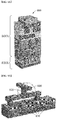
- FIG. 1 illustrates cobalt-tungsten alloy nanowires according to an embodiment.
- the cobalt-tungsten alloy nanowires according to an embodiment are formed by an electroplating method, thereby having an amorphous structure and relatively low electrical resistivity.
- cobalt-tungsten alloy nanowires according to an embodiment serve as a barrier for preventing diffusion into a low-k dielectric of metal wiring and a liner for metal wiring plating, thereby being used as a single layer in a metal wiring process.
- the cobalt-tungsten alloy nanowires 100 may be formed using an electroplating method, a grain structure thereof may be controlled according to the content of tungsten, and electrical resistivity may be reduced through annealing.
- a cobalt-tungsten intermetallic compound may be formed through annealing, thereby reducing electrical resistivity.
- intermetallic compounds may appear at 2 ⁇ of 40.70° ⁇ 0.3°, 43.88° ⁇ 0.3° and 46.46° ⁇ 0.3° when analyzing X-ray diffraction (XRD).
- intermetallic compounds may correspond to XRD peak positions derived during XRD analysis.
- intermetallic compounds of the cobalt-tungsten alloy nanowires 100 will be described in detail below with reference to FIG. 6 .
- annealing may be performed at 25 °C to 600 °C.
- cobalt-tungsten alloy nanowires may be annealed and formed at a temperature of less than 600 °C when used as a barrier, and may be annealed and formed at 600 °C when used as a liner.
- a grain structure of the cobalt-tungsten alloy nanowires 100 may be controlled to have an amorphous-like structure when the content of tungsten is 25.1 at.%.
- a grain structure of the cobalt-tungsten alloy nanowires 100 may be controlled to have a mixed structure including an amorphous-like structure and a polycrystalline structure when the content of tungsten is 15.8 at.% to 19.1 at.%.
- the amorphous-like structure may be a nano-crystalline structure exhibiting the same characteristics as an amorphous structure.
- At least one of a tungsten precursor concentration and a current density may be controlled to control the content of tungsten.
- the cobalt-tungsten alloy nanowires 100 may be formed by an electroplating method using a deionized water-based solution including cobalt sulfate heptahydrate (CoSO 4 ⁇ 7H 2 O) and sodium tungstate heptahydrate (Na 2 WO 4 ⁇ 7H 2 O) which are precursors.
- a deionized water-based solution including cobalt sulfate heptahydrate (CoSO 4 ⁇ 7H 2 O) and sodium tungstate heptahydrate (Na 2 WO 4 ⁇ 7H 2 O) which are precursors.
- the deionized water-based solution may further include boric acid (H 3 BO 3 ) and citric acid (C 6 H 8 O 7 ) as buffers; and sodium citrate tribasic dihydrate (C 6 H 7 Na 3 O 8 ) as an additive.
- boric acid H 3 BO 3
- citric acid C 6 H 8 O 7
- sodium citrate tribasic dihydrate C 6 H 7 Na 3 O 8
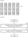
- FIG. 2 illustrates a method of fabricating cobalt-tungsten alloy nanowires according to an embodiment.
- FIG. 2 illustrates a method of fabricating the cobalt-tungsten alloy nanowires according to the embodiment described with reference to FIG. 1 , and thus, contents described in FIG. 1 are omitted in describing FIG. 2 .
- the method of fabricating cobalt-tungsten alloy nanowires uses an electroplating method, thereby being capable of providing cobalt-tungsten alloy nanowires having an amorphous structure and low electrical resistivity.
- the method of fabricating cobalt-tungsten alloy nanowires may provide cobalt-tungsten alloy nanowires that serve as a barrier for preventing diffusion into a low-k dielectric of metal wiring and a liner for metal wiring plating and thus is capable of being used as a single layer in a metal wiring process.
- the method of fabricating cobalt-tungsten alloy nanowires employs a single layer-alloying approach to replace an existing double layer structure.
- the single layer-alloying approach allows realization of an amorphous structure or a grain stuffing effect, thereby being capable of improving barrier properties.
- the amorphous structure allows removal of diffusion paths through grain boundaries, thereby being capable of exhibiting excellent anti-diffusion properties.
- the single-layer alloy material of the cobalt-tungsten alloy nanowires according to an embodiment may have a lower electrical resistivity value than nitride (TaN, resistivity: 160-400 ⁇ cm) while reducing interface resistance caused by a multi-layer structure.
- cobalt-tungsten (Co-W) alloy nanowires may be formed on a nanotemplate using an electroplating method.
- the cobalt-tungsten alloy nanowires formed using an electroplating method may be represented by Co 100-x W x , where the content x of tungsten may be 0 at.% ⁇ x ⁇ 25.1 at.%.
- the nanotemplate may include a polycarbonate membrane (PCM) or anodic aluminum oxide (AAO), and at least one nano-porous track may be formed therein.
- the nano-porous track may be a region where cobalt-tungsten alloy nanowires are deposited through electroplating.
- cobalt-tungsten alloy nanowires may be formed on the nanotemplate by an electroplating method using a deionized water-based solution including cobalt sulfate heptahydrate (CoSO 4 ⁇ 7H 2 O; 0.20 M) and sodium tungstate heptahydrate (Na 2 WO 4 ⁇ 7H 2 O; 0.10 or 0.20 M) which are precursors.
- a deionized water-based solution including cobalt sulfate heptahydrate (CoSO 4 ⁇ 7H 2 O; 0.20 M) and sodium tungstate heptahydrate (Na 2 WO 4 ⁇ 7H 2 O; 0.10 or 0.20 M) which are precursors.
- a deionized water-based solution may further include boric acid (H 3 BO 3 ; 0.65 M) and citric acid (C 6 H 8 O 7 ; 0.04 M), which are buffers, and sodium citrate tribasic dihydrate (C 6 H 7 Na 3 O 8 ; 0.25 or 0.50 M) which is an additive.
- boric acid H 3 BO 3 ; 0.65 M
- citric acid C 6 H 8 O 7 ; 0.04 M
- sodium citrate tribasic dihydrate C 6 H 7 Na 3 O 8 ; 0.25 or 0.50 M
- a grain structure of the alloy nanowires may be controlled according to the content of tungsten.
- the grain structure of the alloy nanowires may be controlled to have an amorphous-like structure by controlling the content of tungsten to 25.1 at.%.
- the grain structure of the alloy nanowires may be controlled to have a mixed structure including an amorphous-like structure and a polycrystalline structure by controlling the content of tungsten to 15.8 at.% to 19.1 at.%.
- the grain structure of the alloy nanowires may be controlled to have an amorphous-like structure by controlling the content of tungsten to 25.1 at.%.
- cobalt-tungsten alloy nanowires having an amorphous structure may be formed by controlling the content of tungsten.
- the content of tungsten may be controlled by controlling at least one of a tungsten precursor concentration and a current density.
- the content of tungsten may be controlled by controlling the concentration of a tungsten precursor solution and a current density in a process of forming cobalt-tungsten alloy nanowires using an electroplating method.
- cobalt-tungsten alloy nanowires may be formed using an electroplating method in an environment in which a current density of 1.25 mA/cm 2 to 5.00 mA/cm 2 is applied to simultaneously reduce cobalt and tungsten.
- the formed alloy nanowires may be annealed.
- the formed alloy nanowires may be separated from the nanotemplate, and the separated alloy nanowires may be annealed.
- a cobalt-tungsten intermetallic compound may be formed through annealing, thereby reducing electrical resistivity of the formed alloy nanowires.
- the formed alloy nanowires may be annealed at 25 °C to 600 °C, preferably at 600 °C.
- the cobalt-tungsten alloy nanowires formed to have an amorphous structure may be annealed, thereby reducing electrical resistivity of the cobalt-tungsten alloy nanowires having an amorphous structure.
- the method of fabricating cobalt-tungsten alloy nanowires according to an embodiment may further include a step of forming a nanotemplate.
- At least one nano-porous track may be formed on a template material and a working electrode layer may be formed on one side surface of the template material on which the nano-porous track has been formed, so as to form a nanotemplate.
- the nanotemplate includes a polycarbonate membrane or anodic aluminum oxide
- the working electrode layer may be at least one of a silver (Ag) electrode and a gold (Au) electrode, preferably may be realized using a silver (Ag) electrode.
- the anodic aluminum oxide may be a porous substrate prepared by oxidizing aluminum using a predetermined acidic solution, and the working electrode layer may be deposited on the polycarbonate membrane or the anodic aluminum oxide using an e-beam evaporator.
- FIGS. 3A to 3D illustrate an example of a method of fabricating cobalt-tungsten alloy nanowires according to an embodiment.
- FIGS. 3A to 3D illustrate an example of a method of fabricating the cobalt-tungsten alloy nanowires according to the embodiment described with reference to FIG. 2 , and thus, contents described in FIG. 2 are omitted in describing FIGS. 3A to 3D .
- a template material 311 may be formed to have at least one nano-porous track to form nanotemplates 311 and 321.
- the nanotemplates 311 and 321 may include a polycarbonate membrane (PCM) or anodic aluminum oxide (AAO).
- PCM polycarbonate membrane
- AAO anodic aluminum oxide
- step 310 of the method of fabricating cobalt-tungsten alloy nanowires regions, in which cobalt-tungsten (Co-W) alloy nanowires 331 are to be formed, of the template material 311 are etched, thereby forming nano-porous tracks.
- a working electrode layer 321 is formed on one side surface of the template material 311 in which nano-porous tracks have been formed, thereby completing the nanotemplates 311 and 321.
- silver (Ag) may be deposited to a thickness of 300 nm on one side surface of the template material 311, in which nano-porous tracks have been formed, using an e-beam evaporator.
- the deposited silver (Ag) may be used as a working electrode to perform an electroplating method, and a platinum (Pt) electrode plate may be used as a counter electrode.
- cobalt-tungsten alloy nanowires 331 may be formed on the nanotemplates 311 and 321 using an electroplating method.
- the cobalt-tungsten alloy nanowires 331 may be formed on the nanotemplates 311 and 321 by an electroplating method in which a deionized water-based solution including cobalt sulfate heptahydrate (CoSO 4 ⁇ 7H 2 O; 0.20 M) and sodium tungstate heptahydrate (Na 2 WO 4 ⁇ 7H 2 O; 0.10 or 0.20 M) which are precursors is used.
- a deionized water-based solution including cobalt sulfate heptahydrate (CoSO 4 ⁇ 7H 2 O; 0.20 M) and sodium tungstate heptahydrate (Na 2 WO 4 ⁇ 7H 2 O; 0.10 or 0.20 M) which are precursors is used.
- the deionized water-based solution may further include boric acid (H 3 BO 3 ; 0.65 M) and citric acid (C 6 H 8 O 7 ; 0.04 M), which are buffers, and sodium citrate tribasic dihydrate (C 6 H 7 Na 3 O 8 ; 0.25 or 0.50 M) which is an additive.
- boric acid H 3 BO 3 ; 0.65 M
- citric acid C 6 H 8 O 7 ; 0.04 M
- sodium citrate tribasic dihydrate C 6 H 7 Na 3 O 8 ; 0.25 or 0.50 M
- a current density of 1.25 mA/cm 2 to 5.00 mA/cm 2 may be applied to simultaneously reduce cobalt and tungsten.
- the grain structure of the alloy nanowires may be controlled according to the content of tungsten.
- the grain structure of the alloy nanowires may be controlled to have an amorphous-like structure when the content of tungsten is 25.1 at.%.
- the grain structure of the alloy nanowires may be controlled to have a mixed structure including an amorphous-like structure and a polycrystalline structure when the content of tungsten is 15.8 at.% to 19.1 at.%.
- the content of tungsten may be controlled by adjusting at least one of a tungsten precursor concentration and a current density.
- the content of tungsten may be controlled by adjusting both the deionized water-based solution including a tungsten precursor and a current density.
- the content of tungsten may be controlled by adjusting the concentrations of sodium tungstate heptahydrate (Na 2 WO 4 ⁇ 7H 2 O), as a tungsten precursor material, and sodium citrate tribasic dihydrate (C 6 H 7 Na 3 O 8 ), as an additive, and a current density in step 330 of the method of fabricating cobalt-tungsten alloy nanowires according to an embodiment.
- Na 2 WO 4 ⁇ 7H 2 O sodium citrate tribasic dihydrate
- C 6 H 7 Na 3 O 8 sodium citrate tribasic dihydrate
- the content of tungsten may be controlled to 25.1 at.% by adjusting the concentration of sodium tungstate heptahydrate (Na 2 WO 4 ⁇ 7H 2 O) to 0.20 mol L -1 , by adjusting the concentration of sodium citrate tribasic dihydrate (C 6 H 7 Na 3 O 8 ) to 0.50 mol L -1 , and by adjusting a current density to 5.00 mA/cm 2 .
- the grain structure of the cobalt-tungsten alloy nanowires may be controlled to have an amorphous-like structure.
- the alloy nanowires 331 may be separated from the nanotemplates 311 and 321.
- a working electrode 321 may be removed with an adhesive tape, and the template material 311 including the alloy nanowires 331 may be selectively removed with a dichloromethane solution (CH 2 Cl 2 ), followed by washing with a chloroform solution (CHCl 3 ) and acetone five or more times through a centrifuge.
- a dichloromethane solution CH 2 Cl 2
- CHCl 3 chloroform solution
- the alloy nanowires 331 present inside the template material 311 may be separated.
- the template material 311 may be selectively removed by stirring for about 15 minutes using 3 M sodium hydroxide (NaOH).
- the separated alloy nanowires 331 may be annealed.
- the formed alloy nanowires may be annealed at 25 °C to 600 °C.
- the alloy nanowires 331 may be annealed at 600 °C.
- FIGS. 4A to 4H illustrates HRTEM and SAED images of cobalt-tungsten alloy nanowires according to an embodiment.
- FIGS. 4A to 4H illustrate high-resolution transmission electron microscope (HRTEM) images and selected-area electron diffraction (SAED) images of cobalt-tungsten alloy nanowires with a diameter of 130 nm formed using various tungsten contents.
- HRTEM transmission electron microscope
- SAED selected-area electron diffraction
- FIGS. 4A and 4B illustrate images of cobalt nanowires in which the content of tungsten is 0.0 at.%
- FIGS. 4C and 4D illustrate images of cobalt-tungsten alloy nanowires in which the content of tungsten is 3.5 at.%
- FIGS. 4E and 4F illustrate images of cobalt-tungsten alloy nanowires in which the content of tungsten is 7.5 at.%
- FIGS. 4G and 4H illustrate images of cobalt-tungsten alloy nanowires in which the content of tungsten is 25.1 at.%.
- the cobalt-tungsten alloy nanowires in which the content of tungsten is 3.5 at% have a polycrystalline structure and thus have lower crystallinity and smaller particle size than pure cobalt nanowires, and the cobalt-tungsten alloy nanowires in which the content of tungsten reaches 15.8 at% have both a nano-crystalline structure (amorphous-like structure) and a polycrystalline structure.
- the cobalt-tungsten alloy nanowires in which the content of tungsten reaches 15.8 at% exhibit a blurry ring pattern as shown in FIG. 4G , which indicates that the nanowires have a nano-crystalline structure (amorphous-like structure) and thus are amorphous.
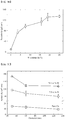
- FIGS. 5A to 5D illustrates XRD analysis results of cobalt-tungsten alloy nanowires according to an embodiment.
- FIG. 5A illustrates an x-ray diffraction (XRD) pattern of cobalt-tungsten alloy nanowires
- FIG. 5B illustrates peak position changes dependent upon tungsten content changes in cobalt-tungsten alloy nanowires
- FIG. 5C illustrates (002) interplanar distance changes dependent upon tungsten content changes in cobalt-tungsten alloy nanowires
- FIG. 5D illustrates grain size changes, which are derived from XRD analysis, dependent upon tungsten content changes in cobalt-tungsten alloy nanowires.
- both the cobalt-tungsten alloy nanowires according to an embodiment and pure cobalt nanowires have an hcp structure.
- the pure cobalt nanowires exhibit a crystalline hcp structure and a strong hcp (002) texture
- the cobalt-tungsten alloy nanowires according to an embodiment exhibit a crystalline hcp structure, similar to the pure cobalt nanowires, and an hcp (002) texture until the content of tungsten increases to 8.5 at%.
- the 2 ⁇ value of the cobalt-tungsten alloy nanowires according to an embodiment changes in response to changes in the tungsten content when the content of tungsten changes within a range of 3.5 at% to 8.5 at%.
- the shift of an XRD peak position of the cobalt-tungsten alloy nanowires according to an embodiment may occur as a result of incorporating tungsten into a cobalt lattice and forming a substitution alloy.
- an average distance may increase when a substituted cobalt-tungsten alloy is formed.
- diffraction peaks of hcp Co(W) (002) are observed at 44.5°, 44.3°, 44.1° and 44° at tungsten contents of 0.0 at%, 3.5 at%, 7.5 at% and 8.5 at%, respectively.
- the interplanar distance d(002) calculated from the XRD pattern linearly increases with increasing content of tungsten, and the increased d(002) value may indicate an increase in electrical resistivity.
- FIG. 5D illustrates grain sizes calculated using the Scherrer equation. From FIG. 5D , it can be confirmed that a grain size of the cobalt-tungsten alloy nanowires according to an embodiment is 38.2 nm when the content of cobalt is 0 at.%, and the grain size is reduced with increasing content of tungsten. Meanwhile, the cobalt-tungsten alloy nanowires according to an embodiment may exhibit an amorphous-like structure when the grain size is smaller than 5 nm.
- the grain size of the cobalt-tungsten alloy nanowires according to an embodiment is reduced with increasing content of tungsten.
- the content of tungsten is 25.1 at.%, the grain size is reduced to 4 nm or less and thus an amorphous-like structure (nano-crystalline structure) is exhibited.
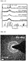
- FIGS. 6A to 6E illustrates annealing temperature-dependent crystallinity characteristic changes of cobalt-tungsten alloy nanowires according to an embodiment.
- FIG. 6A illustrates annealing temperature-dependent XRD analysis results of the cobalt-tungsten alloy nanowires when the content of tungsten is 25.1 at.%
- FIGS. 6B to 6E illustrate SAED patterns of the cobalt-tungsten alloy nanowires when annealing is nor performed, when annealing is performed at 400 °C, when annealing is performed at 500 °C and annealing is performed at 600 °C.
- cobalt-tungsten intermetallic compounds may be formed and thus electrical resistivity may be reduced when the cobalt-tungsten alloy nanowires according to an embodiment are annealed at 600 °C.
- the intermetallic compounds may correspond to an XRD peak position.
- the intermetallic compounds may be observed at 2 ⁇ of 40.70° ⁇ 0.3°, 43.88° ⁇ 0.3° and 46.46° ⁇ 0.3°.
- Annealing temperature-dependent grain sizes and microstrains of the cobalt-tungsten alloy nanowires may be derived as in the following Table 2. [Table 2] Annealing temperature (°C) Grain size, D (nm) Microstrain, ⁇ ( ⁇ 10 -2 ) As-deposited 2.24 4.12 400 2.94 3.12 500 3.77 2.43 600 19.7 0.54
- resistivity values of the cobalt-tungsten alloy nanowires according to an embodiment are reduced to 128.0 ⁇ cm and 120.0 ⁇ cm after being annealed at 400 °C and 500 °C, and a resistivity value is significantly reduced to 87.5 ⁇ cm after being annealed at 600 °C.
- Such resistivity value reduction after annealing may be caused by a grain size increase and release of residual stress.
- microstrain of the cobalt-tungsten alloy nanowires according to an embodiment is also significantly reduced from 4.12 (10 -2 ) to 0.54(10 -2 ).
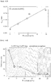
- FIGS. 7A to 7D illustrates electrical property changes dependent upon compositions, nanowire diameters and annealing temperature of cobalt-tungsten alloy nanowires according to an embodiment.
- FIG. 7A illustrates a current (I)-voltage (V) curve of cobalt-tungsten alloy nanowires in which the content of tungsten is 3.5 at.%
- FIG. 7B illustrates a tungsten content change-dependent electrical resistivity change in cobalt-tungsten alloy nanowires
- FIG. 7C illustrates diameter change-dependent electrical resistivity changes in cobalt-tungsten alloy nanowires in which the contents of tungsten are respectively 0.0 at.%, 7.5 at.% and 25.1 at.%
- FIG. 7D illustrates an annealing temperature change-dependent electrical resistivity change in cobalt-tungsten alloy nanowires in which the content of tungsten is 25.1 at.%.
- the current of the cobalt-tungsten alloy nanowires linearly increases according to voltage, and a resistivity value calculated through the I-V curve was 81 ⁇ cm.
- the resistivity value of the cobalt-tungsten alloy nanowires tends to continuously increase with increasing content of tungsten.
- the highest resistivity value thereof is confirmed to be lower than that of a TaN material (160 ⁇ cm to 400 ⁇ cm).
- the resistivity of the cobalt-tungsten alloy nanowires according to an embodiment increases with decreasing diameter thereof regardless of the tungsten content.
- the resistivity value increases to 170 ⁇ cm when the content of tungsten is 25.1 at.% and the diameter is 30 nm.
- the cobalt-tungsten alloy nanowires according to an embodiment have still a lower resistivity value than that of a TaN material (500 ⁇ cm to 1,000 ⁇ cm; thickness: 30 nm).
- the resistivity value of the cobalt-tungsten alloy nanowires according to an embodiment gradually decreases as an annealing temperature increases up to 500°C, and the resistivity value is significantly reduced from 120.0 ⁇ cm to 87.5 ⁇ cm when heat-treated at 600°C.
- FIGS. 8A to 8C illustrates an application example of cobalt-tungsten alloy nanowires according to an embodiment.
- FIG. 8A illustrates a semiconductor device 800 including a back end of line (BEOL) layer and a front end of line (FEOL) layer
- FIG. 8B illustrates a metal line 810 and via 820 included in the BEOL layer of the semiconductor device 800
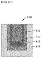
- FIG. 8C illustrates a metal line 810 including a metal layer 811, a liner 812, a barrier 813 and a dielectric 814.
- devices denoted by reference numeral 830 illustrated in FIG. 8B may be transistor elements, and the metal layer 811 may include at least one metal of copper, cobalt and tungsten.
- the cobalt-tungsten alloy nanowires according to an embodiment may be applied in the form of at least one of a barrier and a liner with respect to at least one of the metal line 810, via 820 and contact included in the BEOL layer of the semiconductor device 800.
- the cobalt-tungsten alloy nanowires according to an embodiment may be applied in the form of the liner 812 and barrier 813 formed on the metal layer 811 of the metal line 810.
- the cobalt-tungsten alloy nanowires according to an embodiment may replace a conventional Ta liner and TaN barrier formed on copper metal wiring, thereby preventing rapid resistance increase in the copper metal wiring and thus reducing the thickness of a barrier/liner bilayer.
- the present disclosure provides cobalt-tungsten alloy nanowires having an amorphous structure and low electrical resistivity using an electroplating method.
- the present disclosure provides cobalt-tungsten alloy nanowires that serve as a barrier for preventing diffusion into a low-k dielectric of metal wiring and a liner for metal wiring plating and, accordingly, are used in the form of a single layer in a metal wiring process.
- the present disclosure can provide cobalt-tungsten alloy nanowires having an amorphous structure and low electrical resistivity using an electroplating method.
- the present disclosure can provide cobalt-tungsten alloy nanowires that serve as a barrier for preventing diffusion into a low-k dielectric of metal wiring and a liner for metal wiring plating and, accordingly, are used in the form of a single layer in a metal wiring process.
Landscapes
- Chemical & Material Sciences (AREA)
- Engineering & Computer Science (AREA)
- Organic Chemistry (AREA)
- Materials Engineering (AREA)
- Metallurgy (AREA)
- Chemical Kinetics & Catalysis (AREA)
- Electrochemistry (AREA)
- Crystallography & Structural Chemistry (AREA)
- Nanotechnology (AREA)
- Mechanical Engineering (AREA)
- Physics & Mathematics (AREA)
- Thermal Sciences (AREA)
- Powder Metallurgy (AREA)
- Electroplating And Plating Baths Therefor (AREA)
- Electroplating Methods And Accessories (AREA)
- Electrodes Of Semiconductors (AREA)
- Internal Circuitry In Semiconductor Integrated Circuit Devices (AREA)
Abstract
Description
- This application claims priority to Korean Patent Application No.
10-2020-0065236, filed on May 29, 2020 - The present disclosure relates to a cobalt-tungsten alloy and a method of fabricating the same, and more particularly, to a technical idea of forming cobalt-tungsten alloy nanowires using an electroplating method.
- Copper (Cu) metallization, widely used in processes of fabricating integrated circuits including semiconductor devices, is realized through an electroplating process and a damascene process. Here, a TaN barrier for preventing diffusion into a low-k dielectric surrounding copper metal wiring; and a Ta liner for facilitating Cu plating are required.
- A TaN/Ta double layer structure composed of a barrier layer and liner is important to achieve desired device lifespan, but has much higher electrical resistance than that of Cu metal wiring. In addition, in the case of the TaN/Ta double layer structure, there are difficulties in maintaining a constant thickness (step coverage) on a surface.
- In addition, as the high integration of semiconductors is accelerated, rapid resistance increase in metal wiring negatively affects the entire device in terms of transistor speed, energy consumption, etc. In particular, the thickness of a barrier/liner has reached the limit and thus causes most of wiring resistance.
- Korean Patent No.
10-2088094 - Therefore, the present disclosure has been made in view of the above problems, and it is one object of the present disclosure to provide a cobalt-tungsten alloy capable of forming cobalt-tungsten alloy nanowires having an amorphous structure and low electrical resistivity using an electroplating method; and a method of fabricating the same.
- It is another object of the present disclosure to provide a cobalt-tungsten alloy that serves as a barrier for preventing diffusion into a low-k dielectric of metal wiring and a liner for metal wiring plating and, accordingly, is used in the form of a single layer in a metal wiring process; and a method of fabricating the same.
- In accordance with an aspect of the present disclosure, the above and other objects can be accomplished by the provision of cobalt-tungsten alloy nanowires, wherein the cobalt-tungsten alloy nanowires are formed using an electroplating method, a grain structure of the cobalt-tungsten alloy nanowires is controlled according to a content of tungsten, and electrical resistivity of the cobalt-tungsten alloy nanowires is reduced through annealing.
- According to an embodiment, a cobalt-tungsten intermetallic compound may be formed through the annealing and thus the electrical resistivity may be reduced.
- According to an embodiment, the intermetallic compound may appear at 2θ of 40.70° ± 0.3°, 43.88° ± 0.3° and 46.46° ± 0.3° during x-ray diffraction (XRD) analysis.
- According to an embodiment, the annealing may be performed at 25 °C to 600 °C.
- According to an embodiment, the grain structure may be controlled to have an amorphous-like structure when the content of tungsten is 25.1 at.%.
- According to an embodiment, the grain structure may be controlled to have a mixed structure including an amorphous-like structure and a polycrystalline structure when the content of tungsten is 15.8 at.% to 19.1 at.%.
- According to an embodiment, the content of tungsten may be controlled by adjusting at least one of a tungsten precursor concentration and a current density.
- According to an embodiment, the cobalt-tungsten alloy nanowires may be formed by the electroplating method of using a deionized water-based solution including precursors, cobalt sulfate heptahydrate (CoSO4·7H2O) and sodium tungstate heptahydrate (Na2WO4·7H2O).
- According to an embodiment, the deionized water-based solution may further include boric acid (H3BO3) and citric acid (C6H8O7), as buffers, and sodium citrate tribasic dihydrate (C6H7Na3O8) as an additive.
- According to an embodiment, the cobalt-tungsten alloy nanowires may be applied in the form of at least one of a barrier and a liner with respect to at least one of a via, contact and metal line included in a back end of line (BEOL) layer of a semiconductor device.
- According to an embodiment, the cobalt-tungsten alloy nanowires may be applied in the form of the barrier and the liner on a metal layer of the metal line.
- In accordance with another aspect of the present invention, there is provided a method of fabricating cobalt-tungsten alloy nanowires, the method including: forming cobalt-tungsten (CoW) alloy nanowires on a nanotemplate using an electroplating method; and annealing the formed alloy nanowires, wherein, in the forming, a grain structure of the alloy nanowires is controlled according to a content of tungsten.
- According to an embodiment, in the annealing, a cobalt-tungsten intermetallic compound may be formed through the annealing and thus electrical resistivity may be reduced.
- According to an embodiment, the annealing may be performed at 25 °C to 600 °C.
- According to an embodiment, in the forming, the content of tungsten may be adjusted to 25.1 at.% to control the grain structure of the alloy nanowires to have an amorphous-like structure.
- According to an embodiment, in the forming, the content of tungsten may be adjusted to 15.8 at.% to 19.1 at.% to control the grain structure of the alloy nanowires to have an amorphous-like structure.
- According to an embodiment, in the forming, the cobalt-tungsten alloy nanowires may be formed using the electroplating method in an environment in which a current density of 1.25 mA/cm2 to 5.00 mA/cm2 is applied to simultaneously reduce cobalt and the tungsten.
- According to an embodiment, in the forming, a precursor concentration of the tungsten may be adjusted to 0.20 mol L-1 and a current density may be adjusted to 5.00 mA/cm2 to control the content of tungsten.
- According to an embodiment, the nanotemplate may include a polycarbonate membrane (PCM) or anodic aluminum oxide (AAO) and at least one nano-porous track may be formed in the nanotemplate.
- According to an embodiment, the method of fabricating cobalt-tungsten alloy nanowires may further include separating the annealed alloy nanowires from the nanotemplate.
- The above and other objects, features and other advantages of the present disclosure will be more clearly understood from the following detailed description taken in conjunction with the accompanying drawings, in which:
-
FIG. 1 illustrates cobalt-tungsten alloy nanowires according to an embodiment; -
FIG. 2 illustrates a method of fabricating cobalt-tungsten alloy nanowires according to an embodiment; -
FIGS. 3A to 3D illustrate an example of a method of fabricating cobalt-tungsten alloy nanowires according to an embodiment; -
FIGS. 4A to 4H illustrates HRTEM and SAED images of cobalt-tungsten alloy nanowires according to an embodiment; -
FIGS. 5A to 5D illustrates XRD analysis results of cobalt-tungsten alloy nanowires according to an embodiment; -
FIGS. 6A to 6E illustrates annealing temperature-dependent crystallinity characteristic changes of cobalt-tungsten alloy nanowires according to an embodiment; -
FIGS. 7A to 7D illustrates electrical property changes dependent upon compositions, nanowire diameters and annealing temperature of cobalt-tungsten alloy nanowires according to an embodiment; and -
FIGS. 8A to 8C illustrates an application example of cobalt-tungsten alloy nanowires according to an embodiment. - The embodiments will be described in detail herein with reference to the drawings.
- However, it should be understood that the present disclosure is not limited to the embodiments according to the concept of the present disclosure, but includes changes, equivalents, or alternatives falling within the spirit and scope of the present disclosure.
- In the following description of the present disclosure, a detailed description of known functions and configurations incorporated herein will be omitted when it may make the subject matter of the present disclosure unclear.
- The terms used in the specification are defined in consideration of functions used in the present disclosure, and can be changed according to the intent or conventionally used methods of clients, operators, and users. Accordingly, definitions of the terms should be understood on the basis of the entire description of the present specification.
- In description of the drawings, like reference numerals may be used for similar elements.
- The singular expressions in the present specification may encompass plural expressions unless clearly specified otherwise in context.
- In this specification, expressions such as "A or B" and "at least one of A and/or B" may include all possible combinations of the items listed together.
- Expressions such as "first" and "second" may be used to qualify the elements irrespective of order or importance, and are used to distinguish one element from another and do not limit the elements.
- It will be understood that when an element (e.g., first) is referred to as being "connected to" or "coupled to" another element (e.g., second), it may be directly connected or coupled to the other element or an intervening element (e.g., third) may be present.
- As used herein, "configured to" may be used interchangeably with, for example, "suitable for", "ability to", "changed to", "made to", "capable of", or "designed to" in terms of hardware or software.
- In some situations, the expression "device configured to" may mean that the device "may do ∼" with other devices or components.
- For example, in the sentence "processor configured to perform A, B, and C", the processor may refer to a general purpose processor (e.g., CPU or application processor) capable of performing corresponding operation by running a dedicated processor (e.g., embedded processor) for performing the corresponding operation, or one or more software programs stored in a memory device.
- In addition, the expression "or" means "inclusive or" rather than "exclusive or".
- That is, unless otherwise mentioned or clearly inferred from context, the expression "x uses a or b" means any one of natural inclusive permutations.
- In the above-described specific embodiments, elements included in the invention are expressed singular or plural in accordance with the specific embodiments shown.
- It should be understood, however, that the singular or plural representations are to be chosen as appropriate to the situation presented for the purpose of description and that the above-described embodiments are not limited to the singular or plural constituent elements. The constituent elements expressed in plural may be composed of a single number, and constituent elements expressed in singular form may be composed of a plurality of elements.
- In addition, the present disclosure has been described with reference to exemplary embodiments, but it should be understood that various modifications may be made without departing from the scope of the present disclosure.
- Therefore, the scope of the present disclosure should not be limited by the embodiments, but should be determined by the following claims and equivalents to the following claims.
-
FIG. 1 illustrates cobalt-tungsten alloy nanowires according to an embodiment. - Referring to
FIG. 1 , the cobalt-tungsten alloy nanowires according to an embodiment are formed by an electroplating method, thereby having an amorphous structure and relatively low electrical resistivity. - In addition, the cobalt-tungsten alloy nanowires according to an embodiment serve as a barrier for preventing diffusion into a low-k dielectric of metal wiring and a liner for metal wiring plating, thereby being used as a single layer in a metal wiring process.
- In particular, the cobalt-
tungsten alloy nanowires 100 according to an embodiment may be formed using an electroplating method, a grain structure thereof may be controlled according to the content of tungsten, and electrical resistivity may be reduced through annealing. - According to an embodiment, in the case of the cobalt-
tungsten alloy nanowires 100, a cobalt-tungsten intermetallic compound may be formed through annealing, thereby reducing electrical resistivity. - According to an embodiment, intermetallic compounds may appear at 2θ of 40.70° ± 0.3°, 43.88° ± 0.3° and 46.46° ± 0.3° when analyzing X-ray diffraction (XRD). Here, intermetallic compounds may correspond to XRD peak positions derived during XRD analysis.
- The intermetallic compounds of the cobalt-
tungsten alloy nanowires 100 according to an embodiment will be described in detail below with reference toFIG. 6 . - According to an embodiment, annealing may be performed at 25 °C to 600 °C. For example, cobalt-tungsten alloy nanowires may be annealed and formed at a temperature of less than 600 °C when used as a barrier, and may be annealed and formed at 600 °C when used as a liner.
- According to an embodiment, a grain structure of the cobalt-
tungsten alloy nanowires 100 may be controlled to have an amorphous-like structure when the content of tungsten is 25.1 at.%. - In addition, a grain structure of the cobalt-
tungsten alloy nanowires 100 may be controlled to have a mixed structure including an amorphous-like structure and a polycrystalline structure when the content of tungsten is 15.8 at.% to 19.1 at.%. - Here, since a grain size of the amorphous-like structure is formed as small as that of an amorphous structure, the amorphous-like structure may be a nano-crystalline structure exhibiting the same characteristics as an amorphous structure.
- According to an embodiment, in the case of the cobalt-
tungsten alloy nanowires 100, at least one of a tungsten precursor concentration and a current density may be controlled to control the content of tungsten. - For example, the cobalt-
tungsten alloy nanowires 100 may be formed by an electroplating method using a deionized water-based solution including cobalt sulfate heptahydrate (CoSO4·7H2O) and sodium tungstate heptahydrate (Na2WO4·7H2O) which are precursors. - In addition, the deionized water-based solution may further include boric acid (H3BO3) and citric acid (C6H8O7) as buffers; and sodium citrate tribasic dihydrate (C6H7Na3O8) as an additive.
- The cobalt-tungsten alloy nanowires according to an embodiment will be described in more detail below with reference to
FIGS. 2 to 7 . -
FIG. 2 illustrates a method of fabricating cobalt-tungsten alloy nanowires according to an embodiment. - In other words,
FIG. 2 illustrates a method of fabricating the cobalt-tungsten alloy nanowires according to the embodiment described with reference toFIG. 1 , and thus, contents described inFIG. 1 are omitted in describingFIG. 2 . - Referring to
FIG. 2 , the method of fabricating cobalt-tungsten alloy nanowires according to an embodiment uses an electroplating method, thereby being capable of providing cobalt-tungsten alloy nanowires having an amorphous structure and low electrical resistivity. - In addition, the method of fabricating cobalt-tungsten alloy nanowires according to an embodiment may provide cobalt-tungsten alloy nanowires that serve as a barrier for preventing diffusion into a low-k dielectric of metal wiring and a liner for metal wiring plating and thus is capable of being used as a single layer in a metal wiring process.
- Recently, research and development of a new process using scaling boosters and various materials has been actively conducted, among which a cobalt (Co)-based alloy-based single layer has been identified as a promising material that can replace a TaN/Ta double layer structure having a high specific resistance value.
- Accordingly, the method of fabricating cobalt-tungsten alloy nanowires according to an embodiment employs a single layer-alloying approach to replace an existing double layer structure. The single layer-alloying approach allows realization of an amorphous structure or a grain stuffing effect, thereby being capable of improving barrier properties. In addition, the amorphous structure allows removal of diffusion paths through grain boundaries, thereby being capable of exhibiting excellent anti-diffusion properties.
- In addition, the single-layer alloy material of the cobalt-tungsten alloy nanowires according to an embodiment may have a lower electrical resistivity value than nitride (TaN, resistivity: 160-400 µΩ·cm) while reducing interface resistance caused by a multi-layer structure.
- According to
FIG. 2 , instep 210 of the method of fabricating cobalt-tungsten alloy nanowires according to an embodiment, cobalt-tungsten (Co-W) alloy nanowires may be formed on a nanotemplate using an electroplating method. - For example, the cobalt-tungsten alloy nanowires formed using an electroplating method may be represented by Co100-xWx, where the content x of tungsten may be 0 at.% < x ≤ 25.1 at.%.
- In addition, the nanotemplate may include a polycarbonate membrane (PCM) or anodic aluminum oxide (AAO), and at least one nano-porous track may be formed therein. Here, the nano-porous track may be a region where cobalt-tungsten alloy nanowires are deposited through electroplating.
- According to an embodiment, in
step 210 of the method of fabricating cobalt-tungsten alloy nanowires, cobalt-tungsten alloy nanowires may be formed on the nanotemplate by an electroplating method using a deionized water-based solution including cobalt sulfate heptahydrate (CoSO4·7H2O; 0.20 M) and sodium tungstate heptahydrate (Na2WO4·7H2O; 0.10 or 0.20 M) which are precursors. - In addition, a deionized water-based solution may further include boric acid (H3BO3; 0.65 M) and citric acid (C6H8O7; 0.04 M), which are buffers, and sodium citrate tribasic dihydrate (C6H7Na3O8; 0.25 or 0.50 M) which is an additive.
- Meanwhile, in
step 210 of the method of fabricating cobalt-tungsten alloy nanowires according to an embodiment, a grain structure of the alloy nanowires may be controlled according to the content of tungsten. - According to an embodiment, in
step 210 of the method of fabricating cobalt-tungsten alloy nanowires, the grain structure of the alloy nanowires may be controlled to have an amorphous-like structure by controlling the content of tungsten to 25.1 at.%. - In addition, in
step 210 of the method of fabricating cobalt-tungsten alloy nanowires according to an embodiment, the grain structure of the alloy nanowires may be controlled to have a mixed structure including an amorphous-like structure and a polycrystalline structure by controlling the content of tungsten to 15.8 at.% to 19.1 at.%. - Preferably, in
step 210 of the method of fabricating cobalt-tungsten alloy nanowires according to an embodiment, the grain structure of the alloy nanowires may be controlled to have an amorphous-like structure by controlling the content of tungsten to 25.1 at.%. - That is, by the method of fabricating cobalt-tungsten alloy nanowires according to an embodiment, cobalt-tungsten alloy nanowires having an amorphous structure may be formed by controlling the content of tungsten.
- According to an embodiment, in
step 210 of the method of fabricating cobalt-tungsten alloy nanowires according to an embodiment, the content of tungsten may be controlled by controlling at least one of a tungsten precursor concentration and a current density. - In other words , in
step 210 of the method of fabricating cobalt-tungsten alloy nanowires according to an embodiment, the content of tungsten may be controlled by controlling the concentration of a tungsten precursor solution and a current density in a process of forming cobalt-tungsten alloy nanowires using an electroplating method. - For example, in
step 210 of the method of fabricating cobalt-tungsten alloy nanowires according to an embodiment, cobalt-tungsten alloy nanowires may be formed using an electroplating method in an environment in which a current density of 1.25 mA/cm2 to 5.00 mA/cm2 is applied to simultaneously reduce cobalt and tungsten. - In
step 220 of the method of fabricating cobalt-tungsten alloy nanowires according to an embodiment, the formed alloy nanowires may be annealed. - According to an embodiment, in
step 220 of the method of fabricating cobalt-tungsten alloy nanowires according to an embodiment, the formed alloy nanowires may be separated from the nanotemplate, and the separated alloy nanowires may be annealed. - According to an embodiment, in
step 220 of the method of fabricating cobalt-tungsten alloy nanowires according to an embodiment, a cobalt-tungsten intermetallic compound may be formed through annealing, thereby reducing electrical resistivity of the formed alloy nanowires. - According to an embodiment, in
step 220 of the method of fabricating cobalt-tungsten alloy nanowires according to an embodiment, the formed alloy nanowires may be annealed at 25 °C to 600 °C, preferably at 600 °C. - That is, in the method of fabricating cobalt-tungsten alloy nanowires according to an embodiment, the cobalt-tungsten alloy nanowires formed to have an amorphous structure may be annealed, thereby reducing electrical resistivity of the cobalt-tungsten alloy nanowires having an amorphous structure.
- Meanwhile, the method of fabricating cobalt-tungsten alloy nanowires according to an embodiment may further include a step of forming a nanotemplate.
- More particularly, in the method of fabricating cobalt-tungsten alloy nanowires according to an embodiment, at least one nano-porous track may be formed on a template material and a working electrode layer may be formed on one side surface of the template material on which the nano-porous track has been formed, so as to form a nanotemplate.
- For example, the nanotemplate includes a polycarbonate membrane or anodic aluminum oxide, and the working electrode layer may be at least one of a silver (Ag) electrode and a gold (Au) electrode, preferably may be realized using a silver (Ag) electrode.
- According to an embodiment, the anodic aluminum oxide may be a porous substrate prepared by oxidizing aluminum using a predetermined acidic solution, and the working electrode layer may be deposited on the polycarbonate membrane or the anodic aluminum oxide using an e-beam evaporator.
-
FIGS. 3A to 3D illustrate an example of a method of fabricating cobalt-tungsten alloy nanowires according to an embodiment. - In other words,
FIGS. 3A to 3D illustrate an example of a method of fabricating the cobalt-tungsten alloy nanowires according to the embodiment described with reference toFIG. 2 , and thus, contents described inFIG. 2 are omitted in describingFIGS. 3A to 3D . - Referring to
FIGS. 3A to 3D , instep 310 of the method of fabricating cobalt-tungsten alloy nanowires according to an embodiment, atemplate material 311 may be formed to have at least one nano-porous track to form nanotemplates 311 and 321. - For example, the
nanotemplates - In addition, in
step 310 of the method of fabricating cobalt-tungsten alloy nanowires according to an embodiment, regions, in which cobalt-tungsten (Co-W)alloy nanowires 331 are to be formed, of thetemplate material 311 are etched, thereby forming nano-porous tracks. - In
step 320 of the method of fabricating cobalt-tungsten alloy nanowires according to an embodiment, a workingelectrode layer 321 is formed on one side surface of thetemplate material 311 in which nano-porous tracks have been formed, thereby completing thenanotemplates - For example, in
step 320 of the method of fabricating cobalt-tungsten alloy nanowires according to an embodiment, silver (Ag) may be deposited to a thickness of 300 nm on one side surface of thetemplate material 311, in which nano-porous tracks have been formed, using an e-beam evaporator. - Here, the deposited silver (Ag) may be used as a working electrode to perform an electroplating method, and a platinum (Pt) electrode plate may be used as a counter electrode.
- In
step 330 of the method of fabricating cobalt-tungsten alloy nanowires according to an embodiment, cobalt-tungsten alloy nanowires 331 may be formed on thenanotemplates - For example, in
step 330 of the method of fabricating cobalt-tungsten alloy nanowires according to an embodiment, the cobalt-tungsten alloy nanowires 331 may be formed on thenanotemplates - In addition, the deionized water-based solution may further include boric acid (H3BO3; 0.65 M) and citric acid (C6H8O7; 0.04 M), which are buffers, and sodium citrate tribasic dihydrate (C6H7Na3O8; 0.25 or 0.50 M) which is an additive.
- In addition, in
step 330 of the method of fabricating cobalt-tungsten alloy nanowires according to an embodiment, a current density of 1.25 mA/cm2 to 5.00 mA/cm2 may be applied to simultaneously reduce cobalt and tungsten. - Meanwhile, in
step 330 of the method of fabricating cobalt-tungsten alloy nanowires according to an embodiment, the grain structure of the alloy nanowires may be controlled according to the content of tungsten. - According to an embodiment, in
step 330 of the method of fabricating cobalt-tungsten alloy nanowires, the grain structure of the alloy nanowires may be controlled to have an amorphous-like structure when the content of tungsten is 25.1 at.%. - In addition, in
step 330 of the method of fabricating cobalt-tungsten alloy nanowires according to an embodiment, the grain structure of the alloy nanowires may be controlled to have a mixed structure including an amorphous-like structure and a polycrystalline structure when the content of tungsten is 15.8 at.% to 19.1 at.%. - According to an embodiment, in
step 330 of the method of fabricating cobalt-tungsten alloy nanowires, the content of tungsten may be controlled by adjusting at least one of a tungsten precursor concentration and a current density. - Preferably, in
step 330 of the method of fabricating cobalt-tungsten alloy nanowires according to an embodiment, the content of tungsten may be controlled by adjusting both the deionized water-based solution including a tungsten precursor and a current density. - In particular, according to the following Table 1 in which synthesis conditions by cobalt-tungsten composition are summarized, the content of tungsten may be controlled by adjusting the concentrations of sodium tungstate heptahydrate (Na2WO4·7H2O), as a tungsten precursor material, and sodium citrate tribasic dihydrate (C6H7Na3O8), as an additive, and a current density in
step 330 of the method of fabricating cobalt-tungsten alloy nanowires according to an embodiment.[Table 1] Experimental conditions W-content Na2WO4 (mol L-1) C6H7Na3O8 (mol L-1) Current density (mA/cm2) (at.%) 0.00 0.00 1.25 0.0 0.10 0.25 1.25 3.5 0.10 0.25 5.00 7.5 0.10 0.50 1.25 8.5 0.10 0.50 5.00 15.8 0.20 0.50 1.25 19.1 0.20 0.50 5.00 25.1 - Preferably, in
step 330 of the method of fabricating cobalt-tungsten alloy nanowires according to an embodiment, the content of tungsten may be controlled to 25.1 at.% by adjusting the concentration of sodium tungstate heptahydrate (Na2WO4·7H2O) to 0.20 mol L-1, by adjusting the concentration of sodium citrate tribasic dihydrate (C6H7Na3O8) to 0.50 mol L-1, and by adjusting a current density to 5.00 mA/cm2. Accordingly, the grain structure of the cobalt-tungsten alloy nanowires may be controlled to have an amorphous-like structure. - In
step 340 of the method of fabricating cobalt-tungsten alloy nanowires according to an embodiment, thealloy nanowires 331 may be separated from thenanotemplates - For example, in
step 340 of the method of fabricating cobalt-tungsten alloy nanowires according to an embodiment, a workingelectrode 321 may be removed with an adhesive tape, and thetemplate material 311 including thealloy nanowires 331 may be selectively removed with a dichloromethane solution (CH2Cl2), followed by washing with a chloroform solution (CHCl3) and acetone five or more times through a centrifuge. As a result, thealloy nanowires 331 present inside thetemplate material 311 may be separated. - According to an embodiment, in
step 340 of the method of fabricating cobalt-tungsten alloy nanowires according to an embodiment, thetemplate material 311 may be selectively removed by stirring for about 15 minutes using 3 M sodium hydroxide (NaOH). - In
step 340 of the method of fabricating cobalt-tungsten alloy nanowires according to an embodiment, the separatedalloy nanowires 331 may be annealed. - According to an embodiment, in
step 340 of the method of fabricating cobalt-tungsten alloy nanowires according to an embodiment, the formed alloy nanowires may be annealed at 25 °C to 600 °C. - Preferably, in
step 340 of the method of fabricating cobalt-tungsten alloy nanowires according to an embodiment, thealloy nanowires 331 may be annealed at 600 °C. -
FIGS. 4A to 4H illustrates HRTEM and SAED images of cobalt-tungsten alloy nanowires according to an embodiment. -
FIGS. 4A to 4H illustrate high-resolution transmission electron microscope (HRTEM) images and selected-area electron diffraction (SAED) images of cobalt-tungsten alloy nanowires with a diameter of 130 nm formed using various tungsten contents. - In particular,
FIGS. 4A and 4B illustrate images of cobalt nanowires in which the content of tungsten is 0.0 at.%,FIGS. 4C and 4D illustrate images of cobalt-tungsten alloy nanowires in which the content of tungsten is 3.5 at.%,FIGS. 4E and 4F illustrate images of cobalt-tungsten alloy nanowires in which the content of tungsten is 7.5 at.%, andFIGS. 4G and 4H illustrate images of cobalt-tungsten alloy nanowires in which the content of tungsten is 25.1 at.%. - From
FIGS. 4A to 4H , it can be confirmed that, as a tungsten content in the cobalt-tungsten alloy nanowires increases, interatomic spacing increases and amorphous nanowires are synthesized. - More particularly, from SAED images of
FIGS. 4C ,4E and4G , it can be confirmed that the cobalt-tungsten alloy nanowires in which the content of tungsten is 3.5 at% have a polycrystalline structure and thus have lower crystallinity and smaller particle size than pure cobalt nanowires, and the cobalt-tungsten alloy nanowires in which the content of tungsten reaches 15.8 at% have both a nano-crystalline structure (amorphous-like structure) and a polycrystalline structure. - In addition, the cobalt-tungsten alloy nanowires in which the content of tungsten reaches 15.8 at% exhibit a blurry ring pattern as shown in
FIG. 4G , which indicates that the nanowires have a nano-crystalline structure (amorphous-like structure) and thus are amorphous. -
FIGS. 5A to 5D illustrates XRD analysis results of cobalt-tungsten alloy nanowires according to an embodiment. - Referring to
FIGS. 5A to 5D ,FIG. 5A illustrates an x-ray diffraction (XRD) pattern of cobalt-tungsten alloy nanowires,FIG. 5B illustrates peak position changes dependent upon tungsten content changes in cobalt-tungsten alloy nanowires,FIG. 5C illustrates (002) interplanar distance changes dependent upon tungsten content changes in cobalt-tungsten alloy nanowires, andFIG. 5D illustrates grain size changes, which are derived from XRD analysis, dependent upon tungsten content changes in cobalt-tungsten alloy nanowires. - From
FIG. 5A , it can be confirmed that both the cobalt-tungsten alloy nanowires according to an embodiment and pure cobalt nanowires have an hcp structure. - In particular, it can be confirmed that the pure cobalt nanowires exhibit a crystalline hcp structure and a strong hcp (002) texture, and the cobalt-tungsten alloy nanowires according to an embodiment exhibit a crystalline hcp structure, similar to the pure cobalt nanowires, and an hcp (002) texture until the content of tungsten increases to 8.5 at%.
- In addition, it can be confirmed that the 2θ value of the cobalt-tungsten alloy nanowires according to an embodiment changes in response to changes in the tungsten content when the content of tungsten changes within a range of 3.5 at% to 8.5 at%.
- The shift of an XRD peak position of the cobalt-tungsten alloy nanowires according to an embodiment may occur as a result of incorporating tungsten into a cobalt lattice and forming a substitution alloy.
- An average distance (davg) between two adjacent atoms may be derived from the following Equation 1:

- In addition, a peak position of XRD may be derived from the Bragg equation of the following Equation 2:
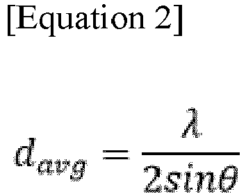
- When tungsten composed of larger atoms enters cobalt which is a host element, significant stress is generated around the host element, which greatly affects electrical properties. In particular, as the content of introduced tungsten (the number of atoms) increases, an average distance (davg) may increase when a substituted cobalt-tungsten alloy is formed.
- In other words, in the case of the cobalt-tungsten alloy nanowires according to an embodiment, it can be confirmed that, as the number of introduced tungsten atoms increases, an average distance (davg) between two adjacent atoms increases when a substituted cobalt-tungsten alloy is formed, resulting in movement of the XRD peak position to a smaller angle.
- Referring to
FIG. 5B , diffraction peaks of hcp Co(W) (002) are observed at 44.5°, 44.3°, 44.1° and 44° at tungsten contents of 0.0 at%, 3.5 at%, 7.5 at% and 8.5 at%, respectively. - Referring to
FIG. 5C , it can be confirmed that the interplanar distance d(002) calculated from the XRD pattern linearly increases with increasing content of tungsten, and the increased d(002) value may indicate an increase in electrical resistivity. -
FIG. 5D illustrates grain sizes calculated using the Scherrer equation. FromFIG. 5D , it can be confirmed that a grain size of the cobalt-tungsten alloy nanowires according to an embodiment is 38.2 nm when the content of cobalt is 0 at.%, and the grain size is reduced with increasing content of tungsten. Meanwhile, the cobalt-tungsten alloy nanowires according to an embodiment may exhibit an amorphous-like structure when the grain size is smaller than 5 nm. - That is, it can be confirmed that the grain size of the cobalt-tungsten alloy nanowires according to an embodiment is reduced with increasing content of tungsten. Particularly, it can be confirmed that, when the content of tungsten is 25.1 at.%, the grain size is reduced to 4 nm or less and thus an amorphous-like structure (nano-crystalline structure) is exhibited.
-
FIGS. 6A to 6E illustrates annealing temperature-dependent crystallinity characteristic changes of cobalt-tungsten alloy nanowires according to an embodiment. - Referring to
FIGS. 6A to 6E ,FIG. 6A illustrates annealing temperature-dependent XRD analysis results of the cobalt-tungsten alloy nanowires when the content of tungsten is 25.1 at.%, andFIGS. 6B to 6E illustrate SAED patterns of the cobalt-tungsten alloy nanowires when annealing is nor performed, when annealing is performed at 400 °C, when annealing is performed at 500 °C and annealing is performed at 600 °C. - Referring to
FIG. 6A , cobalt-tungsten intermetallic compounds may be formed and thus electrical resistivity may be reduced when the cobalt-tungsten alloy nanowires according to an embodiment are annealed at 600 °C. Here, the intermetallic compounds may correspond to an XRD peak position. - Here, the intermetallic compounds may be observed at 2θ of 40.70° ± 0.3°, 43.88° ± 0.3° and 46.46° ± 0.3°.
- More particularly, it can be confirmed that, when the cobalt-tungsten alloy nanowires according to an embodiment are annealed at 400 °C, a single broad XRD peak and a nano-crystalline structure having reduced crystallinity are observed.
- On the other hand, when the cobalt-tungsten alloy nanowires according to an embodiment are annealed at 600 °C, crystallization of the Co3W phase occurs and diffraction patterns of polycrystalline hcp Co3W are observed, and crystallinity is significantly improved.
- In addition, it can be confirmed that, when the cobalt-tungsten alloy nanowires according to an embodiment are annealed at 600 °C, a grain size significantly increases to 19.7 nm. This means that Co3W alloy nanowires are formed after a deposited state present in a solid dissolution state is subjected to heat treatment, which contributes to reduction of internal stress and low resistivity.
- Annealing temperature-dependent grain sizes and microstrains of the cobalt-tungsten alloy nanowires may be derived as in the following Table 2.
[Table 2] Annealing temperature (°C) Grain size, D (nm) Microstrain, ε (×10-2) As-deposited 2.24 4.12 400 2.94 3.12 500 3.77 2.43 600 19.7 0.54 - From
FIGS. 6A to 6E and Table 2, it can be confirmed that annealing temperature-dependent electrical resistivity changes of the cobalt-tungsten alloy nanowires according to an embodiment are inversely proportional to grain sizes. - In particular, it can be confirmed from
FIG. 7D described below that resistivity values of the cobalt-tungsten alloy nanowires according to an embodiment are reduced to 128.0 µΩ·cm and 120.0 µΩ·cm after being annealed at 400 °C and 500 °C, and a resistivity value is significantly reduced to 87.5 µΩ·cm after being annealed at 600 °C. Such resistivity value reduction after annealing may be caused by a grain size increase and release of residual stress. - In addition, it can be confirmed that the microstrain of the cobalt-tungsten alloy nanowires according to an embodiment is also significantly reduced from 4.12 (10-2) to 0.54(10-2).
-
FIGS. 7A to 7D illustrates electrical property changes dependent upon compositions, nanowire diameters and annealing temperature of cobalt-tungsten alloy nanowires according to an embodiment. - Referring to
FIGS. 7A to 7D ,FIG. 7A illustrates a current (I)-voltage (V) curve of cobalt-tungsten alloy nanowires in which the content of tungsten is 3.5 at.%,FIG. 7B illustrates a tungsten content change-dependent electrical resistivity change in cobalt-tungsten alloy nanowires,FIG. 7C illustrates diameter change-dependent electrical resistivity changes in cobalt-tungsten alloy nanowires in which the contents of tungsten are respectively 0.0 at.%, 7.5 at.% and 25.1 at.%, andFIG. 7D illustrates an annealing temperature change-dependent electrical resistivity change in cobalt-tungsten alloy nanowires in which the content of tungsten is 25.1 at.%. - As shown in
FIG. 7A , the current of the cobalt-tungsten alloy nanowires linearly increases according to voltage, and a resistivity value calculated through the I-V curve was 81 µΩ·cm. - In addition, from
FIG. 7B , it can be confirmed that the cobalt-tungsten alloy nanowires in which the content of cobalt is 0 at.% exhibits a resistivity value of 9.4 µΩ·cm, the cobalt-tungsten alloy nanowires in which the content of cobalt is 3.5 at.% exhibits a rapidly increased resistivity value of 72.3 µΩ·cm, and a resistivity value increases up to 133.8 µΩ·cm when the content of cobalt finally increases up to 25.1 at.%. - That is, the resistivity value of the cobalt-tungsten alloy nanowires tends to continuously increase with increasing content of tungsten. However, the highest resistivity value thereof is confirmed to be lower than that of a TaN material (160 µΩ·cm to 400 µΩ·cm).
- From
FIG. 7C , it can be confirmed that the resistivity of the cobalt-tungsten alloy nanowires according to an embodiment increases with decreasing diameter thereof regardless of the tungsten content. In particular, it can be confirmed that the resistivity value increases to 170 µΩ·cm when the content of tungsten is 25.1 at.% and the diameter is 30 nm. - However, it can be confirmed that the cobalt-tungsten alloy nanowires according to an embodiment have still a lower resistivity value than that of a TaN material (500 µΩ·cm to 1,000 µΩ·cm; thickness: 30 nm).
- From
FIG. 7D , it can be confirmed that the resistivity value of the cobalt-tungsten alloy nanowires according to an embodiment gradually decreases as an annealing temperature increases up to 500°C, and the resistivity value is significantly reduced from 120.0 µΩ·cm to 87.5 µΩ·cm when heat-treated at 600°C. -
FIGS. 8A to 8C illustrates an application example of cobalt-tungsten alloy nanowires according to an embodiment. - Referring to
FIGS. 8A to 8C ,FIG. 8A illustrates asemiconductor device 800 including a back end of line (BEOL) layer and a front end of line (FEOL) layer,FIG. 8B illustrates ametal line 810 and via 820 included in the BEOL layer of thesemiconductor device 800, andFIG. 8C illustrates ametal line 810 including ametal layer 811, aliner 812, abarrier 813 and a dielectric 814. - For example, devices denoted by
reference numeral 830 illustrated inFIG. 8B may be transistor elements, and themetal layer 811 may include at least one metal of copper, cobalt and tungsten. - In particular, the cobalt-tungsten alloy nanowires according to an embodiment may be applied in the form of at least one of a barrier and a liner with respect to at least one of the
metal line 810, via 820 and contact included in the BEOL layer of thesemiconductor device 800. - For example, the cobalt-tungsten alloy nanowires according to an embodiment may be applied in the form of the
liner 812 andbarrier 813 formed on themetal layer 811 of themetal line 810. - In other words , the cobalt-tungsten alloy nanowires according to an embodiment may replace a conventional Ta liner and TaN barrier formed on copper metal wiring, thereby preventing rapid resistance increase in the copper metal wiring and thus reducing the thickness of a barrier/liner bilayer.
- In conclusion, the present disclosure provides cobalt-tungsten alloy nanowires having an amorphous structure and low electrical resistivity using an electroplating method.
- In addition, the present disclosure provides cobalt-tungsten alloy nanowires that serve as a barrier for preventing diffusion into a low-k dielectric of metal wiring and a liner for metal wiring plating and, accordingly, are used in the form of a single layer in a metal wiring process.
- In accordance with an embodiment, the present disclosure can provide cobalt-tungsten alloy nanowires having an amorphous structure and low electrical resistivity using an electroplating method.
- In addition, the present disclosure can provide cobalt-tungsten alloy nanowires that serve as a barrier for preventing diffusion into a low-k dielectric of metal wiring and a liner for metal wiring plating and, accordingly, are used in the form of a single layer in a metal wiring process.
- Although the present disclosure has been described with reference to limited embodiments and drawings, it should be understood by those skilled in the art that various changes and modifications may be made therein. For example, the described techniques may be performed in a different order than the described methods, and/or components of the described systems, structures, devices, circuits, etc., may be combined in a manner that is different from the described method, or appropriate results may be achieved even if replaced by other components or equivalents.
- Therefore, other embodiments, other examples, and equivalents to the claims are within the scope of the following claims.
- 100: cobalt-tungsten alloy nanowires
Claims (15)
- Cobalt-tungsten alloy nanowires, wherein the cobalt-tungsten alloy nanowires are formed using an electroplating method, a grain structure of the cobalt-tungsten alloy nanowires is controlled according to a content of tungsten, and electrical resistivity of the cobalt-tungsten alloy nanowires is reduced through annealing.
- The cobalt-tungsten alloy nanowires according to claim 1, wherein a cobalt-tungsten intermetallic compound is formed through the annealing and thus the electrical resistivity is reduced.
- The cobalt-tungsten alloy nanowires according to claim 1, wherein the intermetallic compound appears at 2θ of 40.70° ± 0.3°, 43.88° ± 0.3° and 46.46° ± 0.3° during x-ray diffraction (XRD) analysis.
- The cobalt-tungsten alloy nanowires according to claim 1, wherein the annealing is performed at 25 °C to 600 °C.
- The cobalt-tungsten alloy nanowires according to claim 1, wherein the grain structure is controlled to have an amorphous-like structure when the content of tungsten is 25.1 at.%, and
wherein the grain structure is controlled to have a mixed structure comprising an amorphous-like structure and a polycrystalline structure when the content of tungsten is 15.8 at.% to 19.1 at.%. - The cobalt-tungsten alloy nanowires according to claim 1, wherein the content of tungsten is controlled by adjusting at least one of a tungsten precursor concentration and a current density.
- The cobalt-tungsten alloy nanowires according to claim 1, wherein the cobalt-tungsten alloy nanowires are formed by the electroplating method of using a deionized water-based solution comprising precursors, cobalt sulfate heptahydrate (CoSO4·7H2O) and sodium tungstate heptahydrate (Na2WO4·7H2O), and
wherein the deionized water-based solution further comprises boric acid (H3BO3) and citric acid (C6H8O7), as buffers, and sodium citrate tribasic dihydrate (C6H7Na3O8) as an additive. - The cobalt-tungsten alloy nanowires according to claim 1, wherein the cobalt-tungsten alloy nanowires are applied in the form of at least one of a barrier and a liner with respect to at least one of a via, contact and metal line comprised in a back end of line (BEOL) layer of a semiconductor device.
- The cobalt-tungsten alloy nanowires according to claim 8, wherein the cobalt-tungsten alloy nanowires are applied in the form of the barrier and the liner on a metal layer of the metal line.
- A method of fabricating cobalt-tungsten alloy nanowires, the method comprising:forming cobalt-tungsten (Co-W) alloy nanowires on a nanotemplate using an electroplating method; andannealing the formed alloy nanowires,wherein, in the forming, a grain structure of the alloy nanowires is controlled according to a content of tungsten.
- The method according to claim 10, wherein, in the annealing, a cobalt-tungsten intermetallic compound is formed through the annealing and thus electrical resistivity is reduced, and wherein the annealing is performed at 25 °C to 600 °C.
- The method according to claim 10, wherein, in the forming, the content of tungsten is adjusted to 15.8 at.% to 19.1 at.% or 25.1 at.% to control the grain structure of the alloy nanowires to have an amorphous-like structure.
- The method according to claim 10, wherein, in the forming, the cobalt-tungsten alloy nanowires are formed using the electroplating method in an environment in which a current density of 1.25 mA/cm2 to 5.00 mA/cm2 is applied to simultaneously reduce cobalt and the tungsten.
- The method according to claim 10, wherein, in the forming, a precursor concentration of the tungsten is adjusted to 0.20 mol L-1 and a current density is adjusted to 5.00 mA/cm2 to control the content of tungsten.
- The method according to claim 10, further comprising separating the annealed alloy nanowires from the nanotemplate, and
wherein the nanotemplate comprises a polycarbonate membrane (PCM) or anodic aluminum oxide (AAO) and at least one nano-porous track is formed in the nanotemplate.
Applications Claiming Priority (1)
| Application Number | Priority Date | Filing Date | Title |
|---|---|---|---|
| KR1020200065236A KR102370279B1 (en) | 2020-05-29 | 2020-05-29 | Co-w alloy and manufacturing method thereof |
Publications (1)
| Publication Number | Publication Date |
|---|---|
| EP3916131A1 true EP3916131A1 (en) | 2021-12-01 |
Family
ID=72290965
Family Applications (1)
| Application Number | Title | Priority Date | Filing Date |
|---|---|---|---|
| EP20193449.4A Pending EP3916131A1 (en) | 2020-05-29 | 2020-08-28 | Cobalt-tungsten alloy and method of fabricating the same |
Country Status (4)
| Country | Link |
|---|---|
| US (2) | US20210371959A1 (en) |
| EP (1) | EP3916131A1 (en) |
| JP (1) | JP2021188115A (en) |
| KR (1) | KR102370279B1 (en) |
Citations (3)
| Publication number | Priority date | Publication date | Assignee | Title |
|---|---|---|---|---|
| US20010030366A1 (en) * | 2000-03-08 | 2001-10-18 | Hiroshi Nakano | Semiconducting system and production method |
| KR102088094B1 (en) | 2018-03-12 | 2020-03-11 | 고려대학교 산학협력단 | The Nanoscale Metal Nanowire and The Fabrication Method Of The Same |
| KR20200065236A (en) | 2018-11-30 | 2020-06-09 | 김민지 | a detergent machine |
Family Cites Families (4)
| Publication number | Priority date | Publication date | Assignee | Title |
|---|---|---|---|---|
| SG138479A1 (en) * | 2006-06-15 | 2008-01-28 | Sony Corp | Magnetic anodized aluminium oxide with high oxidation resistance and method for its fabrication |
| JP2012054306A (en) * | 2010-08-31 | 2012-03-15 | Tokyo Electron Ltd | Manufacturing method of semiconductor device |
| US9631291B2 (en) * | 2013-01-29 | 2017-04-25 | Hewlett-Packard Development Company, L.P. | Controlling dimensions of nanowires |
| KR101711888B1 (en) * | 2015-01-16 | 2017-03-03 | 고려대학교 산학협력단 | Metallic nanotube and preparation method thereof |
-
2020
- 2020-05-29 KR KR1020200065236A patent/KR102370279B1/en active Active
- 2020-08-28 US US17/005,519 patent/US20210371959A1/en not_active Abandoned
- 2020-08-28 JP JP2020144598A patent/JP2021188115A/en active Pending
- 2020-08-28 EP EP20193449.4A patent/EP3916131A1/en active Pending
-
2023
- 2023-09-28 US US18/476,663 patent/US12203154B2/en active Active
Patent Citations (3)
| Publication number | Priority date | Publication date | Assignee | Title |
|---|---|---|---|---|
| US20010030366A1 (en) * | 2000-03-08 | 2001-10-18 | Hiroshi Nakano | Semiconducting system and production method |
| KR102088094B1 (en) | 2018-03-12 | 2020-03-11 | 고려대학교 산학협력단 | The Nanoscale Metal Nanowire and The Fabrication Method Of The Same |
| KR20200065236A (en) | 2018-11-30 | 2020-06-09 | 김민지 | a detergent machine |
Non-Patent Citations (1)
| Title |
|---|
| TSYNTSARU N ET AL: "Toward uniform electrodeposition of magnetic Co-W mesowires arrays: direct versus pulse current deposition", ELECTROCHIMICA ACTA, ELSEVIER, AMSTERDAM, NL, vol. 188, 8 December 2015 (2015-12-08), pages 589 - 601, XP029404852, ISSN: 0013-4686, DOI: 10.1016/J.ELECTACTA.2015.12.032 * |
Also Published As
| Publication number | Publication date |
|---|---|
| US20240026496A1 (en) | 2024-01-25 |
| US20210371959A1 (en) | 2021-12-02 |
| JP2021188115A (en) | 2021-12-13 |
| KR20210147667A (en) | 2021-12-07 |
| KR102370279B1 (en) | 2022-03-04 |
| US12203154B2 (en) | 2025-01-21 |
Similar Documents
| Publication | Publication Date | Title |
|---|---|---|
| EP2248164B1 (en) | Microstructure modification in copper interconnect structure | |
| DE112006000465B4 (en) | Semiconductor devices with barrier layers for conductive features and related manufacturing processes | |
| US9082821B2 (en) | Method for forming copper interconnection structures | |
| JP6005160B2 (en) | Metal interconnect structure and method of forming the same (fine structure change in copper interconnect structure) | |
| Shacham-Diamand et al. | Electroless processes for micro-and nanoelectronics | |
| US6440849B1 (en) | Microstructure control of copper interconnects | |
| US6930391B2 (en) | Method for alloy-electroplating group IB metals with refractory metals for interconnections | |
| TWI746383B (en) | Nano-twinned copper layer with doped metal element, substrate comprising the same and method for manufacturing the same | |
| TWI314776B (en) | Composite barrier layer | |
| Moon et al. | Electrical resistivity evolution in electrodeposited Ru and Ru-Co nanowires | |
| Joi et al. | Interface engineering strategy utilizing electrochemical ALD of Cu-Zn for enabling metallization of sub-10 nm semiconductor device nodes | |
| KR101182155B1 (en) | Semiconductor device and method for forming metal thin film | |
| US12203154B2 (en) | Cobalt-tungsten alloy and method of fabricating the same | |
| Chang et al. | Electroless-and electroplating of Cu (Re) alloy films for self-forming ultrathin re diffusion barrier | |
| Papachristos et al. | Effect of annealing on the structure and hardness of Ni–P–W multilayered alloy coatings produced by pulse plating | |
| EP3933071A1 (en) | Ruthenium-based nanowires and method of manufacturing the same | |
| JP6649303B2 (en) | Copper wiring and method of manufacturing the same | |
| KR20240157535A (en) | Molybdenum-based nanometals and manufacturing method thereof | |
| Chang et al. | Thermal stability and interface diffusion behaviors of electrolessly deposited CoWP and Cu films | |
| Xiang et al. | Concurrent enhancement of thermal stability and electrical conductivity of Ta–Cr diffusion-barrier layer with amorphous-crystalline sandwich structure for Cu interconnects | |
| WO2024089972A1 (en) | Silver plating film and electric contact provided with said silver plating film | |
| Chen et al. | Characteristics of Thermally Robust 5 nm Ru–C Diffusion Barrier/Cu Seed Layer in Cu Metallization | |
| Iwasaki et al. | Effect of solid-solution W addition on the nanostructure of electrodeposited Ni |
Legal Events
| Date | Code | Title | Description |
|---|---|---|---|
| PUAI | Public reference made under article 153(3) epc to a published international application that has entered the european phase |
Free format text: ORIGINAL CODE: 0009012 |
|
| STAA | Information on the status of an ep patent application or granted ep patent |
Free format text: STATUS: REQUEST FOR EXAMINATION WAS MADE |
|
| 17P | Request for examination filed |
Effective date: 20200831 |
|
| AK | Designated contracting states |
Kind code of ref document: A1 Designated state(s): AL AT BE BG CH CY CZ DE DK EE ES FI FR GB GR HR HU IE IS IT LI LT LU LV MC MK MT NL NO PL PT RO RS SE SI SK SM TR |
|
| B565 | Issuance of search results under rule 164(2) epc |
Effective date: 20210218 |
|
| RBV | Designated contracting states (corrected) |
Designated state(s): AL AT BE BG CH CY CZ DE DK EE ES FI FR GB GR HR HU IE IS IT LI LT LU LV MC MK MT NL NO PL PT RO RS SE SI SK SM TR |
|
| STAA | Information on the status of an ep patent application or granted ep patent |
Free format text: STATUS: EXAMINATION IS IN PROGRESS |
|
| 17Q | First examination report despatched |
Effective date: 20230531 |