EP3910791A1 - Class-d amplifier with high dynamic range - Google Patents
Class-d amplifier with high dynamic range Download PDFInfo
- Publication number
- EP3910791A1 EP3910791A1 EP21172592.4A EP21172592A EP3910791A1 EP 3910791 A1 EP3910791 A1 EP 3910791A1 EP 21172592 A EP21172592 A EP 21172592A EP 3910791 A1 EP3910791 A1 EP 3910791A1
- Authority
- EP
- European Patent Office
- Prior art keywords
- amplifier
- class
- signal
- switch
- pulse
- Prior art date
- Legal status (The legal status is an assumption and is not a legal conclusion. Google has not performed a legal analysis and makes no representation as to the accuracy of the status listed.)
- Granted
Links
Images



Classifications
-
- H—ELECTRICITY
- H03—ELECTRONIC CIRCUITRY
- H03F—AMPLIFIERS
- H03F3/00—Amplifiers with only discharge tubes or only semiconductor devices as amplifying elements
- H03F3/20—Power amplifiers, e.g. Class B amplifiers, Class C amplifiers
- H03F3/21—Power amplifiers, e.g. Class B amplifiers, Class C amplifiers with semiconductor devices only
- H03F3/217—Class D power amplifiers; Switching amplifiers
- H03F3/2173—Class D power amplifiers; Switching amplifiers of the bridge type
-
- H—ELECTRICITY
- H03—ELECTRONIC CIRCUITRY
- H03F—AMPLIFIERS
- H03F3/00—Amplifiers with only discharge tubes or only semiconductor devices as amplifying elements
- H03F3/20—Power amplifiers, e.g. Class B amplifiers, Class C amplifiers
- H03F3/21—Power amplifiers, e.g. Class B amplifiers, Class C amplifiers with semiconductor devices only
- H03F3/217—Class D power amplifiers; Switching amplifiers
-
- H—ELECTRICITY
- H03—ELECTRONIC CIRCUITRY
- H03F—AMPLIFIERS
- H03F1/00—Details of amplifiers with only discharge tubes, only semiconductor devices or only unspecified devices as amplifying elements
- H03F1/26—Modifications of amplifiers to reduce influence of noise generated by amplifying elements
-
- H—ELECTRICITY
- H03—ELECTRONIC CIRCUITRY
- H03F—AMPLIFIERS
- H03F1/00—Details of amplifiers with only discharge tubes, only semiconductor devices or only unspecified devices as amplifying elements
- H03F1/34—Negative-feedback-circuit arrangements with or without positive feedback
-
- H—ELECTRICITY
- H03—ELECTRONIC CIRCUITRY
- H03F—AMPLIFIERS
- H03F3/00—Amplifiers with only discharge tubes or only semiconductor devices as amplifying elements
- H03F3/181—Low-frequency amplifiers, e.g. audio preamplifiers
-
- H—ELECTRICITY
- H03—ELECTRONIC CIRCUITRY
- H03K—PULSE TECHNIQUE
- H03K19/00—Logic circuits, i.e. having at least two inputs acting on one output; Inverting circuits
- H03K19/20—Logic circuits, i.e. having at least two inputs acting on one output; Inverting circuits characterised by logic function, e.g. AND, OR, NOR, NOT circuits
- H03K19/21—EXCLUSIVE-OR circuits, i.e. giving output if input signal exists at only one input; COINCIDENCE circuits, i.e. giving output only if all input signals are identical
-
- H—ELECTRICITY
- H03—ELECTRONIC CIRCUITRY
- H03F—AMPLIFIERS
- H03F2200/00—Indexing scheme relating to amplifiers
- H03F2200/165—A filter circuit coupled to the input of an amplifier
Definitions
- a class-D audio amplifier is basically a switching amplifier or a pulse width modulation (PWM) amplifier.
- PWM pulse width modulation
- MOSs metal-oxide-silicon transistors
- BD modulation switching technique the duty cycle of the difference between two output signals VOP and VON of the class-D amplifier is modulated to make the average content of the amplified result corresponds to the analog input signal.
- the class-D amplifier is a closed-loop circuit. The larger the analog input signal, the more significant the difference between the two output signals is.
- VON, VOP may be (VDD, VDD) or (GND, GND).
- VON, VOP may be (VDD, VDD) or (GND, GND).
- SNR signal-to-noise ratio
- class-D amplifiers Use of class-D amplifiers is common in audio applications. Any small noise fed to the loop in the no-signal information conditions is intolerable for the user. How to deal with the no-signal information conditions is an important issue in the field of class-D amplifiers.
- a class-D amplifier in accordance with an exemplary embodiment of the present invention includes a loop filter, a pulse-width modulation signal generator, a gate driver, a power driver, and a feedback circuit, which are configured to establish a closed amplification loop.
- the feedback circuit is configured to establish a feedback path.
- the class-D amplifier further includes a feedback breaker. The feedback breaker breaks the feedback path in response to no-signal information conditions of the class-D amplifier.
- the signal-to-noise ratio (SNR) performance is significantly improved.
- an input signal of the class-D amplifier is coupled to the loop filter.
- the loop filter is coupled to the pulse-width modulation signal generator.
- the pulse-width modulation signal generator generates a first pulse-width modulation signal and a second pulse-width modulation signal.
- the gate driver transforms the first pulse-width modulation signal and the second pulse-width modulation signal into control signals.
- the power driver is controlled by the control signals to drive a load.
- the feedback circuit is coupled between the power driver and the loop filter to establish the feedback path. In the no-signal information conditions, the first pulse-width modulation signal may equal the second pulse-width modulation signal.
- the feedback breaker includes a logic circuit and a switch circuit.
- the no-signal information conditions are detected by the logic circuit.
- the logic circuit When detecting the no-signal information conditions, the logic circuit outputs a switch signal to switch the switch circuit to break the feedback path.
- the logic circuit includes an Exclusive-OR gate that receives the first pulse-width modulation signal and the second pulse-width modulation signal to output the switch signal.
- the logic circuit may be combined into the gate driver.
- the logic circuit further includes a delay unit, which delays the switch signal according to the response time of the class-D amplifier.
- the class-D amplifier may be a differential-in and differential-out amplifier, or a single-ended in and single-ended out amplifier.
- FIG. 1 depicts a class-D amplifier in a differential-in and differential-out architecture in accordance with an exemplary embodiment of the present invention.
- the class-D amplifier includes a loop filter 102, a pulse-width modulation (PWM) signal generator 104, a gate driver 106, a power driver 108, and a pair of feedback resistors Rfbp and Rfbn, which are configured to establish a closed amplification loop. A feedback path in the closed amplification loop is established through the feedback resistors Rfbp and Rfbn.
- the class-D amplifier further includes a pair of switches RTO_SWp and RTO_SWn, and a logic circuit 110.
- the logic circuit 110 is operative to detect no-signal information conditions of the class-D amplifier.
- the logic circuit 110 When detecting the no-signal information conditions, the logic circuit 110 outputs a switch signal RTO_clk to disconnect the feedback resistors Rfbp and Rfbn from the positive input terminal Inp and the negative input terminal Inn of the class-D amplifier, respectively. In this manner, the feedback path of the closed amplification loop is broken in response to the no-signal information conditions of the class-D amplifier. No noise is fed into the signal amplification circuit through the feedback path when no meaningful signal is in the signal amplification circuit. The signal-to-noise ratio (SNR) performance, therefore, is significantly improved.
- SNR signal-to-noise ratio
- an input signal (Iinp, linn) of the class-D amplifier is coupled to the loop filter 102.
- the loop filter 102 is coupled to the PWM signal generator 104.
- the PWM signal generator 104 generates PWM signals Vpwmp and Vpwmn by comparing the signals from the loop filter 102 with a saw signal Vsaw.
- the gate driver 106 transforms the PWM signals Vpwmp and Vpwmn into control signals CSAp, CSAn, CSBp, and CSBn.
- the power driver 108 includes an H-bridge circuit controlled by the control signals CSAp, CSAn, CSBp, and CSBn to drive a load 112.
- the feedback resistor Rfbp is coupled between a positive output terminal Vop of the class-D amplifier and a positive input terminal Inp of the class-D amplifier.
- the feedback resistor Rfbn is coupled between a negative output terminal Von of the class-D amplifier and a negative input terminal Inn of the class-D amplifier.
- the PWM signal Vpwmp may equal the PWM signal Vpwmn.
- (VON, VOP) may be (VDD, VDD) or (GND, GND).
- the logic circuit 110 may be combined into the gate driver 106.
- the logic circuit 110 includes an Exclusive-OR gate 114 and a delay unit 116.
- the Exclusive-OR gate 114 receives the PWM signals Vpwmp and Vpwmn, and an output terminal of the Exclusive-OR gate 114 is coupled to the delay unit 116.
- the delay unit 116 provides a delay time according to the response time of the class-D amplifier. In this manner, the switch signal RTO_clk has a proper delay. The feedback path is not broken till all meaningful signals in the amplification circuit have been amplified.
- the delay unit 116 is an optional device.
- the Exclusive-OR calculation is performed on the positive output signal Vop and the negative output signal Von rather than the PWM signals Vpwmp and Vpwmn.
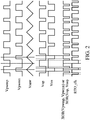
- FIG. 2 shows the waveforms of the signals in the class-D amplifier of FIG. 1 in accordance with an exemplary embodiment of the present invention.
- the status of the PWM signals Vpwmp and Vpwmn is reflected on the positive output signal Vop and the negative output signal Von of the class-D amplifier.
- the PWM signal Vpwmp equals the PWM signal Vpwmn, so that the positive output signal Vop equals the negative output signal Von.
- XOR(Vpwmp,Vpwmn) or XOR(Vop, Von) the identical status of Vpwmp and Vpwmn is detected.
- the switch signal RTO_clk is generated. When the switch signal RTO_clk is high, the switches RTO_SWp and RTO_SWn are open. The feedback path is broken. Noise is not fed into the signal amplification circuit through the feedback path.
- FIG. 3 depicts a class-D amplifier in a single-ended in and single-ended out architecture in accordance with an exemplary embodiment of the present invention.
- the class-D amplifier includes a loop filter 302, a PWM signal generator 304, a gate driver 306, a power driver 308, and a feedback resistor Rfb, which are configured to establish a closed amplification loop. A feedback path in the closed amplification loop is established through the feedback resistor Rfb.
- the class-D amplifier further includes a switch RTO_SW and a logic circuit 310.
- the logic circuit 310 is operative to detect no-signal information conditions of the class-D amplifier.
- the logic circuit 310 When detecting the no-signal information conditions, the logic circuit 310 outputs a switch signal RTO_clk to disconnect the feedback resistor Rfb from the input terminal In of the class-D amplifier, respectively. In this manner, the feedback path of the closed amplification loop is broken in response to the no-signal information conditions of the class-D amplifier. No noise is fed into the signal amplification circuit through the feedback path when no meaningful signal is in the signal amplification circuit. The signal-to-noise ratio (SNR) performance, therefore, is significantly improved.
- SNR signal-to-noise ratio
- an input signal Iin of the class-D amplifier is coupled to the loop filter 302.
- the loop filter 302 is coupled to the PWM signal generator 304.
- the PWM signal generator 304 generates PWM signals Vpwmp and Vpwmn by comparing the signals from the loop filter 302 with a saw signal Vsaw.
- the gate driver 306 transforms the PWM signals Vpwmp and Vpwmn into control signals CSp and CSn.
- the power driver 308 includes transistors Mp, Mn, and Mcm. The transistor Mp is controlled by the control signal CSp and is coupled between a power source terminal (VDD) and an output terminal VOUT of the class-D amplifier.
- the transistor Mn is controlled by the control signal CSn and is coupled between the output terminal VOUT of the class-D amplifier and a negative power source terminal (-VDD).
- the transistor Mcm is controlled by the control signal CScm (e.g., asserted when the PWM signals Vpwmp and Vpwmn are at the same value) and is coupled between the output terminal VOUT of the class-D amplifier and a common-mode node (GND) of the class-D amplifier.
- the power driver 308 drives a load 312.
- the feedback resistor Rfbp is coupled between the output terminal VOUT of the class-D amplifier and the input terminal In of the class-D amplifier.
- the PWM signal Vpwmp may equal the PWM signal Vpwmn.
- (Vpwmp, PWM) may be (VDD, VDD) or (GND, GND).
- the logic circuit 310 may be combined into the gate driver 306.
- the logic circuit 310 includes an Exclusive-OR gate 314 and a delay unit 316.
- the Exclusive-OR gate 314 receives the PWM signals Vpwmp and Vpwmn, and an output terminal of the Exclusive-OR gate 314 is coupled to the delay unit 316.
- the delay unit 316 provides a delay time according to the response time of the class-D amplifier. In this manner, the switch signal RTO_clk has a proper delay. The feedback path is not broken till all meaningful signals in the amplification circuit have been amplified.
- the delay unit 316 is an optional device.
- FIG. 4 shows the waveforms of the signals in the class-D amplifier of FIG. 3 in accordance with an exemplary embodiment of the present invention.
- the PWM signal Vpwmp equals the PWM signal Vpwmn, so that the positive output signal Vop equals the negative output signal Von.
- XOR(Vpwmp,Vpwmn) the identical status of Vpwmp and Vpwmn is detected.
- the switch signal RTO_clk is generated. When the switch signal RTO_clk is high, the switch RTO_SW is open. The feedback path is broken. Noise is not fed into the signal amplification circuit through the feedback path.
- the proposed class-D amplifier includes a loop filter, a pulse-width modulation signal generator, a gate driver, a power driver, and a feedback circuit, which are configured to establish a closed amplification loop.
- the feedback circuit is configured to establish a feedback path.
- the proposed class-D amplifier further includes a feedback breaker. The feedback breaker breaks the feedback path in response to no-signal information conditions of the class-D amplifier.
Landscapes
- Engineering & Computer Science (AREA)
- Power Engineering (AREA)
- Physics & Mathematics (AREA)
- Computer Hardware Design (AREA)
- Computing Systems (AREA)
- General Engineering & Computer Science (AREA)
- Mathematical Physics (AREA)
- Multimedia (AREA)
- Amplifiers (AREA)
Abstract
Description
- A class-D audio amplifier is basically a switching amplifier or a pulse width modulation (PWM) amplifier. In this type of amplifier, the metal-oxide-silicon transistors (MOSs) of the power driver are either fully on or fully off, significantly reducing the power losses in the output stage. A high-efficiency amplification is achieved.
- There are several ways to convert analog signals to PWM signals to drive the MOSs of the power driver. To eliminate an output filter, a BD modulation switching technique is developed. According to the BD modulation switching technique, the duty cycle of the difference between two output signals VOP and VON of the class-D amplifier is modulated to make the average content of the amplified result corresponds to the analog input signal. The class-D amplifier is a closed-loop circuit. The larger the analog input signal, the more significant the difference between the two output signals is.
- However, there are no-signal information conditions in the BD modulation. For example, (VON, VOP) may be (VDD, VDD) or (GND, GND). Under these no-signal information conditions, noise is fed to the loop although no meaningful signal is in the loop. The signal-to-noise ratio (SNR) is degraded.
- Use of class-D amplifiers is common in audio applications. Any small noise fed to the loop in the no-signal information conditions is intolerable for the user. How to deal with the no-signal information conditions is an important issue in the field of class-D amplifiers.
- In the present invention, a solution to deal with conditions in which there is no-signal information is proposed.
- A class-D amplifier in accordance with an exemplary embodiment of the present invention includes a loop filter, a pulse-width modulation signal generator, a gate driver, a power driver, and a feedback circuit, which are configured to establish a closed amplification loop. The feedback circuit is configured to establish a feedback path. The class-D amplifier further includes a feedback breaker. The feedback breaker breaks the feedback path in response to no-signal information conditions of the class-D amplifier.
- In such a design, the signal-to-noise ratio (SNR) performance is significantly improved.
- In an exemplary embodiment, an input signal of the class-D amplifier is coupled to the loop filter. The loop filter is coupled to the pulse-width modulation signal generator. The pulse-width modulation signal generator generates a first pulse-width modulation signal and a second pulse-width modulation signal. The gate driver transforms the first pulse-width modulation signal and the second pulse-width modulation signal into control signals. The power driver is controlled by the control signals to drive a load. The feedback circuit is coupled between the power driver and the loop filter to establish the feedback path. In the no-signal information conditions, the first pulse-width modulation signal may equal the second pulse-width modulation signal.
- In an exemplary embodiment, the feedback breaker includes a logic circuit and a switch circuit. The no-signal information conditions are detected by the logic circuit. When detecting the no-signal information conditions, the logic circuit outputs a switch signal to switch the switch circuit to break the feedback path.
- In an exemplary embodiment, the logic circuit includes an Exclusive-OR gate that receives the first pulse-width modulation signal and the second pulse-width modulation signal to output the switch signal. The logic circuit may be combined into the gate driver.
- In an exemplary embodiment, the logic circuit further includes a delay unit, which delays the switch signal according to the response time of the class-D amplifier.
- The class-D amplifier may be a differential-in and differential-out amplifier, or a single-ended in and single-ended out amplifier.
- A detailed description is given in the following embodiments with reference to the accompanying drawings.
- The present invention can be more fully understood by reading the subsequent detailed description and examples with references made to the accompanying drawings, wherein:
-
FIG. 1 depicts a class-D amplifier in a differential-in and differential-out architecture in accordance with an exemplary embodiment of the present invention; -
FIG. 2 shows the waveforms of the signals in the class-D amplifier ofFIG. 1 in accordance with an exemplary embodiment of the present invention; -
FIG. 3 depicts a class-D amplifier in a single-ended in and single-ended out architecture in accordance with an exemplary embodiment of the present invention; and -
FIG. 4 shows the waveforms of the signals in the class-D amplifier ofFIG. 3 in accordance with an exemplary embodiment of the present invention. - The following description is made for the purpose of illustrating the general principles of the invention and should not be taken in a limiting sense. The scope of the invention is best determined by reference to the appended claims.
-
FIG. 1 depicts a class-D amplifier in a differential-in and differential-out architecture in accordance with an exemplary embodiment of the present invention. The class-D amplifier includes aloop filter 102, a pulse-width modulation (PWM)signal generator 104, agate driver 106, apower driver 108, and a pair of feedback resistors Rfbp and Rfbn, which are configured to establish a closed amplification loop. A feedback path in the closed amplification loop is established through the feedback resistors Rfbp and Rfbn. The class-D amplifier further includes a pair of switches RTO_SWp and RTO_SWn, and alogic circuit 110. Thelogic circuit 110 is operative to detect no-signal information conditions of the class-D amplifier. When detecting the no-signal information conditions, thelogic circuit 110 outputs a switch signal RTO_clk to disconnect the feedback resistors Rfbp and Rfbn from the positive input terminal Inp and the negative input terminal Inn of the class-D amplifier, respectively. In this manner, the feedback path of the closed amplification loop is broken in response to the no-signal information conditions of the class-D amplifier. No noise is fed into the signal amplification circuit through the feedback path when no meaningful signal is in the signal amplification circuit. The signal-to-noise ratio (SNR) performance, therefore, is significantly improved. - As shown, an input signal (Iinp, linn) of the class-D amplifier is coupled to the
loop filter 102. Theloop filter 102 is coupled to thePWM signal generator 104. ThePWM signal generator 104 generates PWM signals Vpwmp and Vpwmn by comparing the signals from theloop filter 102 with a saw signal Vsaw. Thegate driver 106 transforms the PWM signals Vpwmp and Vpwmn into control signals CSAp, CSAn, CSBp, and CSBn. Thepower driver 108 includes an H-bridge circuit controlled by the control signals CSAp, CSAn, CSBp, and CSBn to drive aload 112. The feedback resistor Rfbp is coupled between a positive output terminal Vop of the class-D amplifier and a positive input terminal Inp of the class-D amplifier. The feedback resistor Rfbn is coupled between a negative output terminal Von of the class-D amplifier and a negative input terminal Inn of the class-D amplifier. In the no-signal information conditions, the PWM signal Vpwmp may equal the PWM signal Vpwmn. For example, in the no-signal information conditions, (VON, VOP) may be (VDD, VDD) or (GND, GND). - As shown, the
logic circuit 110 may be combined into thegate driver 106. Thelogic circuit 110 includes an Exclusive-OR gate 114 and adelay unit 116. The Exclusive-OR gate 114 receives the PWM signals Vpwmp and Vpwmn, and an output terminal of the Exclusive-OR gate 114 is coupled to thedelay unit 116. Thedelay unit 116 provides a delay time according to the response time of the class-D amplifier. In this manner, the switch signal RTO_clk has a proper delay. The feedback path is not broken till all meaningful signals in the amplification circuit have been amplified. Thedelay unit 116 is an optional device. - In another exemplary embodiment, the Exclusive-OR calculation is performed on the positive output signal Vop and the negative output signal Von rather than the PWM signals Vpwmp and Vpwmn.
-
FIG. 2 shows the waveforms of the signals in the class-D amplifier ofFIG. 1 in accordance with an exemplary embodiment of the present invention. - The status of the PWM signals Vpwmp and Vpwmn is reflected on the positive output signal Vop and the negative output signal Von of the class-D amplifier. In the no-signal information conditions, the PWM signal Vpwmp equals the PWM signal Vpwmn, so that the positive output signal Vop equals the negative output signal Von. According to an Exclusive-OR calculation, XOR(Vpwmp,Vpwmn) or XOR(Vop, Von), the identical status of Vpwmp and Vpwmn is detected. After a delay depending on the response time of the class-D amplifier, the switch signal RTO_clk is generated. When the switch signal RTO_clk is high, the switches RTO_SWp and RTO_SWn are open. The feedback path is broken. Noise is not fed into the signal amplification circuit through the feedback path.
-
FIG. 3 depicts a class-D amplifier in a single-ended in and single-ended out architecture in accordance with an exemplary embodiment of the present invention. The class-D amplifier includes aloop filter 302, aPWM signal generator 304, agate driver 306, apower driver 308, and a feedback resistor Rfb, which are configured to establish a closed amplification loop. A feedback path in the closed amplification loop is established through the feedback resistor Rfb. The class-D amplifier further includes a switch RTO_SW and alogic circuit 310. Thelogic circuit 310 is operative to detect no-signal information conditions of the class-D amplifier. When detecting the no-signal information conditions, thelogic circuit 310 outputs a switch signal RTO_clk to disconnect the feedback resistor Rfb from the input terminal In of the class-D amplifier, respectively. In this manner, the feedback path of the closed amplification loop is broken in response to the no-signal information conditions of the class-D amplifier. No noise is fed into the signal amplification circuit through the feedback path when no meaningful signal is in the signal amplification circuit. The signal-to-noise ratio (SNR) performance, therefore, is significantly improved. - As shown, an input signal Iin of the class-D amplifier is coupled to the
loop filter 302. Theloop filter 302 is coupled to thePWM signal generator 304. ThePWM signal generator 304 generates PWM signals Vpwmp and Vpwmn by comparing the signals from theloop filter 302 with a saw signal Vsaw. Thegate driver 306 transforms the PWM signals Vpwmp and Vpwmn into control signals CSp and CSn. Thepower driver 308 includes transistors Mp, Mn, and Mcm. The transistor Mp is controlled by the control signal CSp and is coupled between a power source terminal (VDD) and an output terminal VOUT of the class-D amplifier. The transistor Mn is controlled by the control signal CSn and is coupled between the output terminal VOUT of the class-D amplifier and a negative power source terminal (-VDD). The transistor Mcm is controlled by the control signal CScm (e.g., asserted when the PWM signals Vpwmp and Vpwmn are at the same value) and is coupled between the output terminal VOUT of the class-D amplifier and a common-mode node (GND) of the class-D amplifier. Thepower driver 308 drives aload 312. The feedback resistor Rfbp is coupled between the output terminal VOUT of the class-D amplifier and the input terminal In of the class-D amplifier. In the no-signal information conditions, the PWM signal Vpwmp may equal the PWM signal Vpwmn. For example, in the no-signal information conditions, (Vpwmp, PWM) may be (VDD, VDD) or (GND, GND). - As shown, the
logic circuit 310 may be combined into thegate driver 306. Thelogic circuit 310 includes an Exclusive-OR gate 314 and adelay unit 316. The Exclusive-OR gate 314 receives the PWM signals Vpwmp and Vpwmn, and an output terminal of the Exclusive-OR gate 314 is coupled to thedelay unit 316. Thedelay unit 316 provides a delay time according to the response time of the class-D amplifier. In this manner, the switch signal RTO_clk has a proper delay. The feedback path is not broken till all meaningful signals in the amplification circuit have been amplified. Thedelay unit 316 is an optional device. -
FIG. 4 shows the waveforms of the signals in the class-D amplifier ofFIG. 3 in accordance with an exemplary embodiment of the present invention. - In the no-signal information conditions, the PWM signal Vpwmp equals the PWM signal Vpwmn, so that the positive output signal Vop equals the negative output signal Von. According to an Exclusive-OR calculation, XOR(Vpwmp,Vpwmn), the identical status of Vpwmp and Vpwmn is detected. After a delay depending on the response time of the class-D amplifier, the switch signal RTO_clk is generated. When the switch signal RTO_clk is high, the switch RTO_SW is open. The feedback path is broken. Noise is not fed into the signal amplification circuit through the feedback path.
- There may be various modifications in the class-D amplification circuit. Any class-D amplifier with the following components should be considered within the scope of the present invention. The proposed class-D amplifier includes a loop filter, a pulse-width modulation signal generator, a gate driver, a power driver, and a feedback circuit, which are configured to establish a closed amplification loop. The feedback circuit is configured to establish a feedback path. The proposed class-D amplifier further includes a feedback breaker. The feedback breaker breaks the feedback path in response to no-signal information conditions of the class-D amplifier.
- While the invention has been described by way of example and in terms of the preferred embodiments, it should be understood that the invention is not limited to the disclosed embodiments. On the contrary, it is intended to cover various modifications and similar arrangements (as would be apparent to those skilled in the art). Therefore, the scope of the appended claims should be accorded the broadest interpretation so as to encompass all such modifications and similar arrangements.
Claims (15)
- A class-D amplifier, comprising:a loop filter (102/302), a pulse-width modulation signal generator (104/304), a gate driver (106/306), a power driver (108/308), and a feedback circuit (Rfbp and Rfbn/Rfb), configured to establish a closed amplification loop, wherein the feedback circuit is configured to establish a feedback path; anda feedback breaker (110, RTO_SWp and RTO_SWn/ 310 and RTO_SW), breaking the feedback path in response to no-signal information conditions of the class-D amplifier.
- The class-D amplifier as claimed in claim 1, wherein:an input signal of the class-D amplifier is coupled to the loop filter;the loop filter is coupled to the pulse-width modulation signal generator;the pulse-width modulation signal generator generates a first pulse-width modulation signal (Vpwmp) and a second pulse-width modulation signal (Vpwmn);the gate driver transforms the first pulse-width modulation signal and the second pulse-width modulation signal into control signals (CSAp, CSAn, CSBp, and CSBn/CSp, CSn, and CScm);the power driver is controlled by the control signals to drive a load (112/312); andthe feedback circuit is coupled between the power driver and the loop filter to establish the feedback path.
- The class-D amplifier as claimed in claim 2, wherein:
in the no-signal information conditions, the first pulse-width modulation signal equals the second pulse-width modulation signal. - The class-D amplifier as claimed in claim 3, wherein:the feedback breaker includes a logic circuit (110/310) and a switch circuit (RTO_SWp and RTO_SWn/ RTO_SW);the no-signal information conditions are detected by the logic circuit; andwhen detecting the no-signal information conditions, the logic circuit outputs a switch signal (RTO_clk) to switch the switch circuit to break the feedback path.
- The class-D amplifier as claimed in claim 4, wherein:
the logic circuit includes an Exclusive-OR gate (114/314) that receives the first pulse-width modulation signal and the second pulse-width modulation signal to output the switch signal. - The class-D amplifier as claimed in claim 5, wherein:
the logic circuit is combined into the gate driver. - The class-D amplifier as claimed in claim 5 or 6, wherein:
the logic circuit further includes a delay unit (116/316), which delays the switch signal according to a response time of the class-D amplifier. - The class-D amplifier as claimed in claim 4, which is a differential-in and differential-out amplifier (FIG. 1), wherein:the feedback circuit includes a first feedback resistor (Rfbp) coupled between a positive output terminal of the class-D amplifier and a positive input terminal of the class-D amplifier, and a second feedback resistor and (Rfbn) coupled between a negative output terminal of the class-D amplifier and a negative input terminal of the class-D amplifier; andthe switch circuit includes a first switch (RTO_SWp) operative to disconnect the first feedback resistor from the positive input terminal of the class-D amplifier, and a second switch (RTO_SWn) operative to disconnect the second feedback resistor from the negative input terminal of the class-D amplifier.
- The class-D amplifier as claimed in claim 8, wherein:
the power driver includes an H-bridge circuit. - The class-D amplifier as claimed in claim 9, wherein:the logic circuit includes an Exclusive-OR gate (114) that receives the first pulse-width modulation signal and the second pulse-width modulation signal to output the switch signal; andthe first switch and the second switch are opened by the switch signal.
- The class-D amplifier as claimed in claim 10, wherein:
the logic circuit further includes a delay unit (116), which delays the switch signal according to the response time of the class-D amplifier. - The class-D amplifier as claimed in claim 4, which is a single-ended in and single-ended out amplifier (FIG. 3), wherein:the feedback circuit includes a feedback resistor (Rfb) coupled between an output terminal of the class-D amplifier and an input terminal of the class-D amplifier; andthe switch circuit includes a switch (RTO_SW) operative to disconnect the feedback resistor from the input terminal of the class-D amplifier.
- The class-D amplifier as claimed in claim 12, wherein the power driver includes a first transistor (Mp), a second transistor (Mn), and a third transistor (Mcm) controlled by the gate driver, wherein:the first transistor is coupled between a power source terminal and the output terminal of the class-D amplifier;the second transistor is coupled between the output terminal of the class-D amplifier and a negative power source terminal; andthe third transistor is coupled between the output terminal of the class-D amplifier and a common-mode node of the class-D amplifier.
- The class-D amplifier as claimed in claim 13, wherein:the logic circuit includes an Exclusive-OR gate (314) that receives the first pulse-width modulation signal and the second pulse-width modulation signal to output the switch signal; andthe switch is opened by the switch signal.
- The class-D amplifier as claimed in claim 14, wherein:
the logic circuit further includes a delay unit (316), which delays the switch signal according to the response time of the class-D amplifier.
Applications Claiming Priority (2)
| Application Number | Priority Date | Filing Date | Title |
|---|---|---|---|
| US202063023915P | 2020-05-13 | 2020-05-13 | |
| US17/227,583 US11552602B2 (en) | 2020-05-13 | 2021-04-12 | Class-D amplifier with high dynamic range |
Publications (2)
| Publication Number | Publication Date |
|---|---|
| EP3910791A1 true EP3910791A1 (en) | 2021-11-17 |
| EP3910791B1 EP3910791B1 (en) | 2023-03-29 |
Family
ID=75825733
Family Applications (1)
| Application Number | Title | Priority Date | Filing Date |
|---|---|---|---|
| EP21172592.4A Active EP3910791B1 (en) | 2020-05-13 | 2021-05-06 | Class-d amplifier with high dynamic range |
Country Status (4)
| Country | Link |
|---|---|
| US (1) | US11552602B2 (en) |
| EP (1) | EP3910791B1 (en) |
| CN (1) | CN113676144B (en) |
| TW (1) | TWI746405B (en) |
Families Citing this family (1)
| Publication number | Priority date | Publication date | Assignee | Title |
|---|---|---|---|---|
| TWI828359B (en) * | 2022-10-07 | 2024-01-01 | 立錡科技股份有限公司 | Class-d amplifier circuit |
Citations (3)
| Publication number | Priority date | Publication date | Assignee | Title |
|---|---|---|---|---|
| US20110006843A1 (en) * | 2006-07-07 | 2011-01-13 | Yamaha Corporation | Offset voltage correction circuit and class D amplifier |
| EP2375566A1 (en) * | 2010-04-12 | 2011-10-12 | Dialog Semiconductor GmbH | Duplicate feedback network in class D amplifiers |
| CN109756817B (en) * | 2017-11-03 | 2020-04-10 | 福州瑞芯微电子股份有限公司 | Class D audio amplifier and noise suppression method thereof |
Family Cites Families (12)
| Publication number | Priority date | Publication date | Assignee | Title |
|---|---|---|---|---|
| JP2004146981A (en) * | 2002-10-23 | 2004-05-20 | Sharp Corp | Class D amplifier |
| JP2005322957A (en) * | 2004-05-06 | 2005-11-17 | Nec Electronics Corp | Class d amplifier |
| CN100438292C (en) * | 2006-11-09 | 2008-11-26 | 北京航空航天大学 | Digital switch power amplifier for magnetic suspension flywheel magnetic bearing system |
| EP2221964B1 (en) | 2009-02-18 | 2015-06-24 | Hypex Electronics B.V. | Self oscillating class D amplification device |
| EP2481150A4 (en) * | 2009-09-22 | 2013-11-20 | Nokia Corp | ADJUSTABLE CIRCUIT ARCHITECTURE |
| JP5388362B2 (en) * | 2010-03-11 | 2014-01-15 | パナソニック株式会社 | Digital amplifier |
| JP2012060613A (en) * | 2010-09-13 | 2012-03-22 | Uinzu:Kk | Self excitation type oscillation circuit, and class d amplifier device |
| GB2550243B (en) | 2014-08-29 | 2018-03-21 | Cirrus Logic Int Semiconductor Ltd | Class D amplifier circuit |
| CN105048980B (en) * | 2015-08-18 | 2018-09-18 | 矽力杰半导体技术(杭州)有限公司 | A class D audio amplifier |
| EP3416285B1 (en) | 2017-06-16 | 2021-06-02 | ICEpower a/s | Self-oscillating amplifier system |
| US10608606B2 (en) * | 2017-06-23 | 2020-03-31 | Skyworks Solutions, Inc. | Power amplifier noise suppression using feedback |
| US10476455B1 (en) | 2018-08-08 | 2019-11-12 | Cirrus Logic, Inc. | Apparatus and method of suppressing transient noise during transition for class-D amplifier system having one or more pulse width modulator output paths |
-
2021
- 2021-04-12 US US17/227,583 patent/US11552602B2/en active Active
- 2021-05-03 TW TW110115849A patent/TWI746405B/en active
- 2021-05-06 EP EP21172592.4A patent/EP3910791B1/en active Active
- 2021-05-06 CN CN202110491382.2A patent/CN113676144B/en active Active
Patent Citations (3)
| Publication number | Priority date | Publication date | Assignee | Title |
|---|---|---|---|---|
| US20110006843A1 (en) * | 2006-07-07 | 2011-01-13 | Yamaha Corporation | Offset voltage correction circuit and class D amplifier |
| EP2375566A1 (en) * | 2010-04-12 | 2011-10-12 | Dialog Semiconductor GmbH | Duplicate feedback network in class D amplifiers |
| CN109756817B (en) * | 2017-11-03 | 2020-04-10 | 福州瑞芯微电子股份有限公司 | Class D audio amplifier and noise suppression method thereof |
Also Published As
| Publication number | Publication date |
|---|---|
| CN113676144A (en) | 2021-11-19 |
| EP3910791B1 (en) | 2023-03-29 |
| TW202143639A (en) | 2021-11-16 |
| US11552602B2 (en) | 2023-01-10 |
| CN113676144B (en) | 2025-05-27 |
| US20210359653A1 (en) | 2021-11-18 |
| TWI746405B (en) | 2021-11-11 |
Similar Documents
| Publication | Publication Date | Title |
|---|---|---|
| US9425744B2 (en) | Multi mode bias modulator operating in envelope tracking mode or average power tracking mode and envelope tracking power amplifier using the same | |
| US9559637B2 (en) | Multi-mode bias modulator and envelope tracking power amplifier using the same | |
| US8284953B2 (en) | Circuit and method of reducing pop-up noise in a digital amplifier | |
| US8054123B2 (en) | Fast differential level shifter and boot strap driver including the same | |
| US7973598B2 (en) | Audio power amplifier and a pre-amplifier thereof | |
| US6614310B2 (en) | Zero-overhead class G amplifier with threshold detection | |
| CN102792586A (en) | Digital amplifier | |
| JP4786879B2 (en) | Class D power amplifier and method for preventing an excessive response phenomenon that occurs when returning from an abnormal state to a steady state | |
| JP4765316B2 (en) | Power amplifier device | |
| US6992527B2 (en) | Digital power amplifier | |
| JP2009060361A (en) | Class-d amplifier circuit | |
| US11171617B2 (en) | Power amplifying device and audio equipment | |
| KR100420887B1 (en) | Audio signal amplifier | |
| US11552602B2 (en) | Class-D amplifier with high dynamic range | |
| CN115459721B (en) | Audio power amplifier circuit | |
| JP2007088921A (en) | Speaker protection circuit | |
| KR100770747B1 (en) | Digital Amplifier and Voice Playback Method | |
| US7388431B2 (en) | Switching amplifier and control method thereof | |
| TWI334268B (en) | Class-d audio amplifier with half-swing pulse-width-modulation | |
| US20230091797A1 (en) | Power amplifying device | |
| US6967530B2 (en) | Circuit and semiconductor device for reducing the generation of shock noise of a power amplifier outputting amplified audio signals | |
| JP4772719B2 (en) | Power amplifier | |
| KR101110291B1 (en) | Pulse operating apparatus for audio power switch | |
| KR20250105076A (en) | Amplifying circuit and amplifying device | |
| JPH06152268A (en) | Switching amplifier |
Legal Events
| Date | Code | Title | Description |
|---|---|---|---|
| PUAI | Public reference made under article 153(3) epc to a published international application that has entered the european phase |
Free format text: ORIGINAL CODE: 0009012 |
|
| STAA | Information on the status of an ep patent application or granted ep patent |
Free format text: STATUS: THE APPLICATION HAS BEEN PUBLISHED |
|
| AK | Designated contracting states |
Kind code of ref document: A1 Designated state(s): AL AT BE BG CH CY CZ DE DK EE ES FI FR GB GR HR HU IE IS IT LI LT LU LV MC MK MT NL NO PL PT RO RS SE SI SK SM TR |
|
| B565 | Issuance of search results under rule 164(2) epc |
Effective date: 20211001 |
|
| STAA | Information on the status of an ep patent application or granted ep patent |
Free format text: STATUS: REQUEST FOR EXAMINATION WAS MADE |
|
| 17P | Request for examination filed |
Effective date: 20220329 |
|
| RBV | Designated contracting states (corrected) |
Designated state(s): AL AT BE BG CH CY CZ DE DK EE ES FI FR GB GR HR HU IE IS IT LI LT LU LV MC MK MT NL NO PL PT RO RS SE SI SK SM TR |
|
| GRAP | Despatch of communication of intention to grant a patent |
Free format text: ORIGINAL CODE: EPIDOSNIGR1 |
|
| STAA | Information on the status of an ep patent application or granted ep patent |
Free format text: STATUS: GRANT OF PATENT IS INTENDED |
|
| INTG | Intention to grant announced |
Effective date: 20221028 |
|
| GRAS | Grant fee paid |
Free format text: ORIGINAL CODE: EPIDOSNIGR3 |
|
| GRAA | (expected) grant |
Free format text: ORIGINAL CODE: 0009210 |
|
| STAA | Information on the status of an ep patent application or granted ep patent |
Free format text: STATUS: THE PATENT HAS BEEN GRANTED |
|
| AK | Designated contracting states |
Kind code of ref document: B1 Designated state(s): AL AT BE BG CH CY CZ DE DK EE ES FI FR GB GR HR HU IE IS IT LI LT LU LV MC MK MT NL NO PL PT RO RS SE SI SK SM TR |
|
| REG | Reference to a national code |
Ref country code: CH Ref legal event code: EP |
|
| REG | Reference to a national code |
Ref country code: DE Ref legal event code: R096 Ref document number: 602021001719 Country of ref document: DE |
|
| REG | Reference to a national code |
Ref country code: AT Ref legal event code: REF Ref document number: 1557376 Country of ref document: AT Kind code of ref document: T Effective date: 20230415 |
|
| REG | Reference to a national code |
Ref country code: IE Ref legal event code: FG4D |
|
| REG | Reference to a national code |
Ref country code: LT Ref legal event code: MG9D |
|
| P01 | Opt-out of the competence of the unified patent court (upc) registered |
Effective date: 20230607 |
|
| PG25 | Lapsed in a contracting state [announced via postgrant information from national office to epo] |
Ref country code: RS Free format text: LAPSE BECAUSE OF FAILURE TO SUBMIT A TRANSLATION OF THE DESCRIPTION OR TO PAY THE FEE WITHIN THE PRESCRIBED TIME-LIMIT Effective date: 20230329 Ref country code: NO Free format text: LAPSE BECAUSE OF FAILURE TO SUBMIT A TRANSLATION OF THE DESCRIPTION OR TO PAY THE FEE WITHIN THE PRESCRIBED TIME-LIMIT Effective date: 20230629 Ref country code: LV Free format text: LAPSE BECAUSE OF FAILURE TO SUBMIT A TRANSLATION OF THE DESCRIPTION OR TO PAY THE FEE WITHIN THE PRESCRIBED TIME-LIMIT Effective date: 20230329 Ref country code: LT Free format text: LAPSE BECAUSE OF FAILURE TO SUBMIT A TRANSLATION OF THE DESCRIPTION OR TO PAY THE FEE WITHIN THE PRESCRIBED TIME-LIMIT Effective date: 20230329 Ref country code: HR Free format text: LAPSE BECAUSE OF FAILURE TO SUBMIT A TRANSLATION OF THE DESCRIPTION OR TO PAY THE FEE WITHIN THE PRESCRIBED TIME-LIMIT Effective date: 20230329 |
|
| REG | Reference to a national code |
Ref country code: NL Ref legal event code: MP Effective date: 20230329 |
|
| REG | Reference to a national code |
Ref country code: AT Ref legal event code: MK05 Ref document number: 1557376 Country of ref document: AT Kind code of ref document: T Effective date: 20230329 |
|
| PG25 | Lapsed in a contracting state [announced via postgrant information from national office to epo] |
Ref country code: SE Free format text: LAPSE BECAUSE OF FAILURE TO SUBMIT A TRANSLATION OF THE DESCRIPTION OR TO PAY THE FEE WITHIN THE PRESCRIBED TIME-LIMIT Effective date: 20230329 Ref country code: NL Free format text: LAPSE BECAUSE OF FAILURE TO SUBMIT A TRANSLATION OF THE DESCRIPTION OR TO PAY THE FEE WITHIN THE PRESCRIBED TIME-LIMIT Effective date: 20230329 Ref country code: GR Free format text: LAPSE BECAUSE OF FAILURE TO SUBMIT A TRANSLATION OF THE DESCRIPTION OR TO PAY THE FEE WITHIN THE PRESCRIBED TIME-LIMIT Effective date: 20230630 Ref country code: FI Free format text: LAPSE BECAUSE OF FAILURE TO SUBMIT A TRANSLATION OF THE DESCRIPTION OR TO PAY THE FEE WITHIN THE PRESCRIBED TIME-LIMIT Effective date: 20230329 |
|
| PG25 | Lapsed in a contracting state [announced via postgrant information from national office to epo] |
Ref country code: SM Free format text: LAPSE BECAUSE OF FAILURE TO SUBMIT A TRANSLATION OF THE DESCRIPTION OR TO PAY THE FEE WITHIN THE PRESCRIBED TIME-LIMIT Effective date: 20230329 Ref country code: RO Free format text: LAPSE BECAUSE OF FAILURE TO SUBMIT A TRANSLATION OF THE DESCRIPTION OR TO PAY THE FEE WITHIN THE PRESCRIBED TIME-LIMIT Effective date: 20230329 Ref country code: PT Free format text: LAPSE BECAUSE OF FAILURE TO SUBMIT A TRANSLATION OF THE DESCRIPTION OR TO PAY THE FEE WITHIN THE PRESCRIBED TIME-LIMIT Effective date: 20230731 Ref country code: ES Free format text: LAPSE BECAUSE OF FAILURE TO SUBMIT A TRANSLATION OF THE DESCRIPTION OR TO PAY THE FEE WITHIN THE PRESCRIBED TIME-LIMIT Effective date: 20230329 Ref country code: EE Free format text: LAPSE BECAUSE OF FAILURE TO SUBMIT A TRANSLATION OF THE DESCRIPTION OR TO PAY THE FEE WITHIN THE PRESCRIBED TIME-LIMIT Effective date: 20230329 Ref country code: AT Free format text: LAPSE BECAUSE OF FAILURE TO SUBMIT A TRANSLATION OF THE DESCRIPTION OR TO PAY THE FEE WITHIN THE PRESCRIBED TIME-LIMIT Effective date: 20230329 |
|
| PG25 | Lapsed in a contracting state [announced via postgrant information from national office to epo] |
Ref country code: SK Free format text: LAPSE BECAUSE OF FAILURE TO SUBMIT A TRANSLATION OF THE DESCRIPTION OR TO PAY THE FEE WITHIN THE PRESCRIBED TIME-LIMIT Effective date: 20230329 Ref country code: PL Free format text: LAPSE BECAUSE OF FAILURE TO SUBMIT A TRANSLATION OF THE DESCRIPTION OR TO PAY THE FEE WITHIN THE PRESCRIBED TIME-LIMIT Effective date: 20230329 Ref country code: IS Free format text: LAPSE BECAUSE OF FAILURE TO SUBMIT A TRANSLATION OF THE DESCRIPTION OR TO PAY THE FEE WITHIN THE PRESCRIBED TIME-LIMIT Effective date: 20230729 |
|
| REG | Reference to a national code |
Ref country code: DE Ref legal event code: R097 Ref document number: 602021001719 Country of ref document: DE |
|
| PG25 | Lapsed in a contracting state [announced via postgrant information from national office to epo] |
Ref country code: MC Free format text: LAPSE BECAUSE OF FAILURE TO SUBMIT A TRANSLATION OF THE DESCRIPTION OR TO PAY THE FEE WITHIN THE PRESCRIBED TIME-LIMIT Effective date: 20230329 |
|
| REG | Reference to a national code |
Ref country code: BE Ref legal event code: MM Effective date: 20230531 |
|
| PG25 | Lapsed in a contracting state [announced via postgrant information from national office to epo] |
Ref country code: MC Free format text: LAPSE BECAUSE OF FAILURE TO SUBMIT A TRANSLATION OF THE DESCRIPTION OR TO PAY THE FEE WITHIN THE PRESCRIBED TIME-LIMIT Effective date: 20230329 Ref country code: LU Free format text: LAPSE BECAUSE OF NON-PAYMENT OF DUE FEES Effective date: 20230506 Ref country code: DK Free format text: LAPSE BECAUSE OF FAILURE TO SUBMIT A TRANSLATION OF THE DESCRIPTION OR TO PAY THE FEE WITHIN THE PRESCRIBED TIME-LIMIT Effective date: 20230329 Ref country code: CZ Free format text: LAPSE BECAUSE OF FAILURE TO SUBMIT A TRANSLATION OF THE DESCRIPTION OR TO PAY THE FEE WITHIN THE PRESCRIBED TIME-LIMIT Effective date: 20230329 |
|
| PLBE | No opposition filed within time limit |
Free format text: ORIGINAL CODE: 0009261 |
|
| STAA | Information on the status of an ep patent application or granted ep patent |
Free format text: STATUS: NO OPPOSITION FILED WITHIN TIME LIMIT |
|
| REG | Reference to a national code |
Ref country code: IE Ref legal event code: MM4A |
|
| 26N | No opposition filed |
Effective date: 20240103 |
|
| PG25 | Lapsed in a contracting state [announced via postgrant information from national office to epo] |
Ref country code: IE Free format text: LAPSE BECAUSE OF NON-PAYMENT OF DUE FEES Effective date: 20230506 |
|
| PG25 | Lapsed in a contracting state [announced via postgrant information from national office to epo] |
Ref country code: IE Free format text: LAPSE BECAUSE OF NON-PAYMENT OF DUE FEES Effective date: 20230506 |
|
| PG25 | Lapsed in a contracting state [announced via postgrant information from national office to epo] |
Ref country code: SI Free format text: LAPSE BECAUSE OF FAILURE TO SUBMIT A TRANSLATION OF THE DESCRIPTION OR TO PAY THE FEE WITHIN THE PRESCRIBED TIME-LIMIT Effective date: 20230329 |
|
| PG25 | Lapsed in a contracting state [announced via postgrant information from national office to epo] |
Ref country code: SI Free format text: LAPSE BECAUSE OF FAILURE TO SUBMIT A TRANSLATION OF THE DESCRIPTION OR TO PAY THE FEE WITHIN THE PRESCRIBED TIME-LIMIT Effective date: 20230329 Ref country code: IT Free format text: LAPSE BECAUSE OF FAILURE TO SUBMIT A TRANSLATION OF THE DESCRIPTION OR TO PAY THE FEE WITHIN THE PRESCRIBED TIME-LIMIT Effective date: 20230329 Ref country code: BE Free format text: LAPSE BECAUSE OF NON-PAYMENT OF DUE FEES Effective date: 20230531 |
|
| PG25 | Lapsed in a contracting state [announced via postgrant information from national office to epo] |
Ref country code: BG Free format text: LAPSE BECAUSE OF FAILURE TO SUBMIT A TRANSLATION OF THE DESCRIPTION OR TO PAY THE FEE WITHIN THE PRESCRIBED TIME-LIMIT Effective date: 20230329 |
|
| PG25 | Lapsed in a contracting state [announced via postgrant information from national office to epo] |
Ref country code: BG Free format text: LAPSE BECAUSE OF FAILURE TO SUBMIT A TRANSLATION OF THE DESCRIPTION OR TO PAY THE FEE WITHIN THE PRESCRIBED TIME-LIMIT Effective date: 20230329 |
|
| REG | Reference to a national code |
Ref country code: CH Ref legal event code: PL |
|
| PG25 | Lapsed in a contracting state [announced via postgrant information from national office to epo] |
Ref country code: CH Free format text: LAPSE BECAUSE OF NON-PAYMENT OF DUE FEES Effective date: 20240531 |
|
| PGFP | Annual fee paid to national office [announced via postgrant information from national office to epo] |
Ref country code: DE Payment date: 20250325 Year of fee payment: 5 |
|
| PG25 | Lapsed in a contracting state [announced via postgrant information from national office to epo] |
Ref country code: CY Free format text: LAPSE BECAUSE OF FAILURE TO SUBMIT A TRANSLATION OF THE DESCRIPTION OR TO PAY THE FEE WITHIN THE PRESCRIBED TIME-LIMIT; INVALID AB INITIO Effective date: 20210506 |
|
| PG25 | Lapsed in a contracting state [announced via postgrant information from national office to epo] |
Ref country code: HU Free format text: LAPSE BECAUSE OF FAILURE TO SUBMIT A TRANSLATION OF THE DESCRIPTION OR TO PAY THE FEE WITHIN THE PRESCRIBED TIME-LIMIT; INVALID AB INITIO Effective date: 20210506 |
|
| PG25 | Lapsed in a contracting state [announced via postgrant information from national office to epo] |
Ref country code: TR Free format text: LAPSE BECAUSE OF FAILURE TO SUBMIT A TRANSLATION OF THE DESCRIPTION OR TO PAY THE FEE WITHIN THE PRESCRIBED TIME-LIMIT Effective date: 20230329 |
|
| PGFP | Annual fee paid to national office [announced via postgrant information from national office to epo] |
Ref country code: GB Payment date: 20260313 Year of fee payment: 6 |
|
| PGFP | Annual fee paid to national office [announced via postgrant information from national office to epo] |
Ref country code: FR Payment date: 20260309 Year of fee payment: 6 |