EP3910787A1 - Electromagnetic wave transmission device and electromagnetic wave communication system - Google Patents
Electromagnetic wave transmission device and electromagnetic wave communication system Download PDFInfo
- Publication number
- EP3910787A1 EP3910787A1 EP20739078.2A EP20739078A EP3910787A1 EP 3910787 A1 EP3910787 A1 EP 3910787A1 EP 20739078 A EP20739078 A EP 20739078A EP 3910787 A1 EP3910787 A1 EP 3910787A1
- Authority
- EP
- European Patent Office
- Prior art keywords
- electromagnetic wave
- voltage
- signal
- value
- modulation
- Prior art date
- Legal status (The legal status is an assumption and is not a legal conclusion. Google has not performed a legal analysis and makes no representation as to the accuracy of the status listed.)
- Granted
Links
Images


Classifications
-
- H—ELECTRICITY
- H04—ELECTRIC COMMUNICATION TECHNIQUE
- H04L—TRANSMISSION OF DIGITAL INFORMATION, e.g. TELEGRAPHIC COMMUNICATION
- H04L27/00—Modulated-carrier systems
- H04L27/02—Amplitude-modulated carrier systems, e.g. using on-off keying; Single sideband or vestigial sideband modulation
- H04L27/04—Modulator circuits; Transmitter circuits
-
- H—ELECTRICITY
- H03—ELECTRONIC CIRCUITRY
- H03B—GENERATION OF OSCILLATIONS, DIRECTLY OR BY FREQUENCY-CHANGING, BY CIRCUITS EMPLOYING ACTIVE ELEMENTS WHICH OPERATE IN A NON-SWITCHING MANNER; GENERATION OF NOISE BY SUCH CIRCUITS
- H03B7/00—Generation of oscillations using active element having a negative resistance between two of its electrodes
- H03B7/02—Generation of oscillations using active element having a negative resistance between two of its electrodes with frequency-determining element comprising lumped inductance and capacitance
- H03B7/06—Generation of oscillations using active element having a negative resistance between two of its electrodes with frequency-determining element comprising lumped inductance and capacitance active element being semiconductor device
- H03B7/08—Generation of oscillations using active element having a negative resistance between two of its electrodes with frequency-determining element comprising lumped inductance and capacitance active element being semiconductor device being a tunnel diode
-
- H—ELECTRICITY
- H03—ELECTRONIC CIRCUITRY
- H03B—GENERATION OF OSCILLATIONS, DIRECTLY OR BY FREQUENCY-CHANGING, BY CIRCUITS EMPLOYING ACTIVE ELEMENTS WHICH OPERATE IN A NON-SWITCHING MANNER; GENERATION OF NOISE BY SUCH CIRCUITS
- H03B7/00—Generation of oscillations using active element having a negative resistance between two of its electrodes
- H03B7/02—Generation of oscillations using active element having a negative resistance between two of its electrodes with frequency-determining element comprising lumped inductance and capacitance
- H03B7/06—Generation of oscillations using active element having a negative resistance between two of its electrodes with frequency-determining element comprising lumped inductance and capacitance active element being semiconductor device
-
- H—ELECTRICITY
- H03—ELECTRONIC CIRCUITRY
- H03C—MODULATION
- H03C7/00—Modulating electromagnetic waves
-
- H—ELECTRICITY
- H04—ELECTRIC COMMUNICATION TECHNIQUE
- H04B—TRANSMISSION
- H04B1/00—Details of transmission systems, not covered by a single one of groups H04B3/00 - H04B13/00; Details of transmission systems not characterised by the medium used for transmission
- H04B1/02—Transmitters
- H04B1/04—Circuits
Definitions
- the present invention relates to an electromagnetic wave transmission apparatus and an electromagnetic wave communication system.
- an amplitude-shift keying modulation method (hereinafter referred to as ASK modulation method) is known.
- ASK modulation method an amplitude-shift keying modulation method
- OOK modulation method an on-off keying modulation method
- Patent Document 1 discloses a technique related to the ASK modulation method using a resonant tunneling diode (hereinafter referred to as RTD) as an oscillating element for electromagnetic wave transmission.
- the technique is a technique that represents a binary value by switching between data in an oscillation region of the RTD (for example, a signal corresponding to On) and data in a non-oscillation region (for example, a signal corresponding to Off), that is, a technique for representing On and Off by a difference in amplitude.
- the RTD has the local maximum value and the local minimum value located on the higher voltage side than the local maximum value in the voltage-current characteristics.
- the voltage value at the local maximum value is defined as a voltage value V OL
- the voltage value at the local minimum value is defined as a voltage value V OH .
- a spectrum of a current from the voltage value V OL to the voltage value V OH is a differential negative resistance region showing differential negative resistance characteristics.
- the differential negative resistance region is defined as the oscillation region RA. That is, the RTD has a differential negative resistance region (oscillation region RA) showing the differential negative resistance characteristics in the voltage-current characteristics of an operating region.
- the electromagnetic wave reception apparatus 30 receives the electromagnetic wave W transmitted by the electromagnetic wave transmission apparatus 20 and demodulates the received electromagnetic wave W into a digital signal. For example, in a case where the digital signal is a signal obtained by digitizing sound, the electromagnetic wave reception apparatus 30 generates a detection timing based on the synchronization signal data among the electromagnetic waves W received by the electromagnetic wave reception apparatus 30, and demodulates the digital signal of the sound.
- the digital signal is a signal obtained by digitizing sound
- the electromagnetic wave reception apparatus 30 generates a detection timing based on the synchronization signal data among the electromagnetic waves W received by the electromagnetic wave reception apparatus 30, and demodulates the digital signal of the sound.
- the electromagnetic wave communication system 10 of the present embodiment will be described with reference to the drawings.
- the overall flow will be described first, and then a specific example of multi-value modulation will be described.
- the electromagnetic wave communication system 10 is used to communicate signals related to sound.
- the effects of the present embodiment will be described together with the following description.
- the transmission unit 28 transmits the data selected and input by the selector 26B on the electromagnetic wave W. That is, the transmission unit 28 transmits the electromagnetic wave W indicating a modulation signal for the data.
- the electromagnetic wave transmission apparatus 20 of the present embodiment can transmit a synchronization signal that is easily recognized by the electromagnetic wave reception apparatus 30. Accordingly, the electromagnetic wave communication system 10 of the present embodiment has high communication stability in terms of recognizability of the synchronization signal.
Landscapes
- Engineering & Computer Science (AREA)
- Computer Networks & Wireless Communication (AREA)
- Signal Processing (AREA)
- Physics & Mathematics (AREA)
- Electromagnetism (AREA)
- Transmitters (AREA)
- Near-Field Transmission Systems (AREA)
- Dc Digital Transmission (AREA)
- Synchronisation In Digital Transmission Systems (AREA)
Abstract
Description
- The present invention relates to an electromagnetic wave transmission apparatus and an electromagnetic wave communication system.
- As a modulation method for communication used for an oscillating element for electromagnetic wave transmission, an amplitude-shift keying modulation method (hereinafter referred to as ASK modulation method) is known. In addition, as a modulation method for communication, an on-off keying modulation method (hereinafter referred to as an OOK modulation method) is also known as one method included in the ASK modulation method.
- Here, Patent Document 1 discloses a technique related to the ASK modulation method using a resonant tunneling diode (hereinafter referred to as RTD) as an oscillating element for electromagnetic wave transmission. Specifically, the technique is a technique that represents a binary value by switching between data in an oscillation region of the RTD (for example, a signal corresponding to On) and data in a non-oscillation region (for example, a signal corresponding to Off), that is, a technique for representing On and Off by a difference in amplitude.
- In addition, Patent Document 2 discloses a technique related to an ASK modulation method using a terahertz wave of continuous oscillation such as RTD. Specifically, the technique is a technique in which variable light having variable intensity is superimposed and incident on a modulation element as signal light, and the amplitude of the terahertz wave is modulated according to the signal intensity.
-
- [Patent Document 1]
Japanese Unexamined Patent Publication No. 2012-191520 - [Patent Document 2]
Japanese Unexamined Patent Publication No. 2010-41204 - However, since the techniques disclosed in Patent Document 1 and Patent Document 2 are techniques that represent a binary value due to differences in amplitude, there is a limit to increasing the transmission speed (or communication speed).
- As an example of the problem to be solved by the present invention, increasing the transmission speed can be included.
- The invention according to claim 1 is an electromagnetic wave transmission apparatus including a transmission unit whose voltage-current characteristics have a local maximum value and a local minimum value located on a higher voltage side than the local maximum value and which transmits an electromagnetic wave indicating a modulation signal, an acquisition unit which acquires a digital signal, and a modulation unit which modulates the digital signal into the modulation signal which is a signal using voltage values of three levels or more in an oscillation region which is a voltage region that is equal to or more than a voltage of the local maximum value and equal to or less than a voltage of the local minimum value.
- The above-described objectives and other objectives, features, and advantages will be further clarified by the preferred embodiments described below and the accompanying drawings below.
-
-
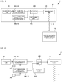
Fig. 1 is a schematic view of an electromagnetic wave communication system of the present embodiment. -
Fig. 2 is a schematic view of an electromagnetic wave transmission apparatus included in an electromagnetic wave communication system of the present embodiment. -
Fig. 3 is a graph showing voltage-current characteristics of an element for oscillating an electromagnetic wave included in an electromagnetic wave transmission apparatus of the present embodiment and voltage values of four levels in an oscillation region. -
Fig. 4 is an example of a modulation signal transmitted by the electromagnetic wave transmission apparatus of the present embodiment. -
Fig. 5 is another example of a modulation signal transmitted by the electromagnetic wave transmission apparatus of the present embodiment. - Hereinafter, the present embodiment (an example of the present invention) will be described. First, functions and configurations of an electromagnetic wave communication system 10 (refer to
Fig. 1 ) of the present embodiment will be described with reference to the drawings. Next, operation of the electromagneticwave communication system 10 of the present embodiment will be described with reference to the drawings. The effect of the present embodiment will be described in the description of the operation. In all the drawings to be referred to, components having the same function are designated by the same reference numerals, and the description thereof will not be repeated. -
Fig. 1 is a schematic view of an electromagneticwave communication system 10 of the present embodiment. The electromagneticwave communication system 10 includes an electromagneticwave transmission apparatus 20 and an electromagneticwave reception apparatus 30. The electromagneticwave communication system 10 has a function of receiving an electromagnetic wave W transmitted by the electromagneticwave transmission apparatus 20 by the electromagneticwave reception apparatus 30. - The electromagnetic wave W of the present embodiment is an electromagnetic wave indicating a modulation signal described later. In addition, the electromagnetic wave W of the present embodiment is a terahertz wave as an example. Here, the terahertz wave is referred to as an electromagnetic wave having a shorter wavelength than millimeter waves and a longer wavelength than infrared rays. The terahertz wave is an electromagnetic wave having both properties of an optical wave and a radio wave, and has, for example, a property of transmitting (or easily transmitting) cloth, paper, wood, plastic, ceramics, or the like, and not transmitting (or hardly transmitting) metal, water, or the like. Generally, the frequency of the terahertz wave is also referred to as an electromagnetic wave of around 1 THz (wavelength corresponds to around 300 µm), but there is generally no clear definition of the range. Therefore, in the present specification, the wavelength range of the terahertz wave is defined as a range of 70 GHz or more and 10 THz or less.
-
Fig. 2 is a schematic view of an electromagneticwave transmission apparatus 20 of the present embodiment. The electromagneticwave transmission apparatus 20 has a function of transmitting the electromagnetic wave W indicating a modulation signal that is subjected to multi-value modulation. The electromagneticwave transmission apparatus 20 includes, as an example, anacquisition unit 22, a conversion unit 24 (an example of a modulation unit), aswitching unit 26A, aselector 26B, atransmission unit 28, a multi-valuelevel setting unit 29A, and a synchronizationlevel setting unit 29B. - The
acquisition unit 22 of the present embodiment has a function of acquiring digital signals such as sound and video as an example. In addition, theacquisition unit 22 has a function of outputting the acquired digital signal to theconversion unit 24. - As an example, the
conversion unit 24 of the present embodiment includes the multi-valuelevel conversion unit 24A and the synchronization signallevel conversion unit 24B. - The multi-value
level conversion unit 24A has a function of receiving a digital signal (data for communication) from theacquisition unit 22, converting the digital signal into a multi-value level signal according to the multi-value level setting, and outputting the signal. Here, the multi-value level setting means setting a voltage level of three levels or more in an oscillation region RA (refer toFig. 3 ) described later. - In addition, the synchronization signal
level conversion unit 24B has a function of outputting a predetermined synchronization signal level according to the synchronization level setting. Here, the synchronization level setting means setting a voltage level of three levels or more in an oscillation region RA (refer toFig. 3 ) . - The
switching unit 26A has a function of generating a switching timing of data selected by theselector 26B and output to thetransmission unit 28 and inputting the data to theselector 26B. Here, the data are data (hereinafter referred to as multi- value data) output by the multi-valuelevel conversion unit 24A and data (hereinafter referred to as synchronization signal data) output by the synchronization signallevel conversion unit 24B. - The
selector 26B has a function of outputting the synchronization signal data and the multi-value data to thetransmission unit 28 at different timings according to the switching timing of the data generated by theswitching unit 26A. - The
transmission unit 28 has a function of oscillating the data selected and input by theselector 26B as an electromagnetic wave W (in the case of this embodiment, the terahertz wave as described above). Therefore, thetransmission unit 28 has an element that oscillates the terahertz wave. The element that oscillates the terahertz wave of the present embodiment is an RTD as an example. However, the element does not have to be an RTD as long as it is an element that oscillates the terahertz wave. - Here, the voltage-current characteristics of RTD (characteristics of current with respect to voltage in a two-dimensional graph showing a relationship between voltage and current) will be described with reference to the graph of
Fig. 3. Fig. 3 is a graph showing voltage-current characteristics of RTD of the present embodiment and voltage values of four levels in an oscillation region RA. - The RTD has the local maximum value and the local minimum value located on the higher voltage side than the local maximum value in the voltage-current characteristics. Here, the voltage value at the local maximum value is defined as a voltage value VOL, and the voltage value at the local minimum value is defined as a voltage value VOH. A spectrum of a current from the voltage value VOL to the voltage value VOH is a differential negative resistance region showing differential negative resistance characteristics. In the present specification, the differential negative resistance region is defined as the oscillation region RA. That is, the RTD has a differential negative resistance region (oscillation region RA) showing the differential negative resistance characteristics in the voltage-current characteristics of an operating region. Then, the RTD functions as the element that oscillates the electromagnetic wave W when the voltage value in the oscillation region RA is applied. Both sides of the oscillation region RA in the graph of voltage-current characteristics correspond to the non-oscillation region of the RTD. Here, the non-oscillation region of the RTD means a region other than the voltage region for oscillating the electromagnetic wave W in the voltage-current characteristics of the RTD. In the present specification, a region on the lower voltage side than the voltage value VOL among the non-oscillation regions is defined as a non-oscillation region RB, and a region on the higher voltage side than the voltage value VOH is defined as a non-oscillation region RC.
- Then, when the synchronization signal data from the synchronization signal
level conversion unit 24B is input, thetransmission unit 28 transmits a synchronization signal having the pattern corresponding to the voltage values of three levels or more in the oscillation region RA. Here, the synchronization signal of the present embodiment is a signal for informing the electromagneticwave reception apparatus 30 of a detection timing of the transmission signal, and also has a role of causing the electromagneticwave reception apparatus 30 to recognize a part or all of the voltage levels used for the modulation signal. Next, when the multi-value data from the multi-valuelevel conversion unit 24A is input, thetransmission unit 28 transmits a digital signal having the pattern corresponding to the voltage values of three levels or more in the oscillation region RA. Here, the voltage values of three levels or more in the present embodiment are voltage values of four levels as an example. - As described above, the multi-value level setting and the synchronization level setting in the present embodiment are set to the voltage values of four levels in the oscillation region RA. In addition, the electromagnetic
wave transmission apparatus 20 of the present embodiment performs multi-value modulation on the multi-value data and the synchronization signal data, and transmits data subjected to the multi-value modulation to the electromagneticwave reception apparatus 30 on the electromagnetic wave W. - The electromagnetic
wave reception apparatus 30 receives the electromagnetic wave W transmitted by the electromagneticwave transmission apparatus 20 and demodulates the received electromagnetic wave W into a digital signal. For example, in a case where the digital signal is a signal obtained by digitizing sound, the electromagneticwave reception apparatus 30 generates a detection timing based on the synchronization signal data among the electromagnetic waves W received by the electromagneticwave reception apparatus 30, and demodulates the digital signal of the sound. - The above is the description of the configuration of the present embodiment.
- Next, operation of the electromagnetic
wave communication system 10 of the present embodiment will be described with reference to the drawings. Hereinafter, the overall flow will be described first, and then a specific example of multi-value modulation will be described. As an example, the electromagneticwave communication system 10 is used to communicate signals related to sound. In addition, as described above, the effects of the present embodiment will be described together with the following description. - Hereinafter, the overall flow of the operation of the present embodiment will be described with reference to
Figs. 1 and 2 . - First, the
acquisition unit 22 acquires a digital signal related to sound from an external apparatus (not shown in the drawings), and outputs the acquired digital signal to the conversion unit 24 (multi-valuelevel conversion unit 24A). - Next, the multi-value
level conversion unit 24A receives the digital signal (data for communication) from theacquisition unit 22, converts it to the multi-value level according to the multi-value level setting by the multi-valuelevel setting unit 29A, and outputs it. In addition, the synchronization signallevel conversion unit 24B outputs a predetermined synchronization signal level according to the synchronization level setting by the synchronizationlevel setting unit 29B. - Next, the
switching unit 26A generates a switching timing between the multi-value data and the synchronization signal data that are selected by theselector 26B and are output to thetransmission unit 28, and inputs the switching timing to theselector 26B. As a result, theselector 26B outputs the synchronization signal data and the multi-value data to thetransmission unit 28 at different timings according to the switching timing generated by theswitching unit 26A. - Next, the
transmission unit 28 transmits the data selected and input by theselector 26B on the electromagnetic wave W. That is, thetransmission unit 28 transmits the electromagnetic wave W indicating a modulation signal for the data. - Next, the electromagnetic
wave reception apparatus 30 receives the electromagnetic wave W transmitted by the transmission unit 28 (electromagnetic wave transmission apparatus 20), generates a detection timing based on the synchronization signal data among the received electromagnetic waves W, and demodulates the multi-value data into the digital signal. As a result, the electromagnetic wave W received by the electromagneticwave reception apparatus 30 is demodulated into the digital signal of the sound. - The above is the description of the overall flow of the operation of the present embodiment.
- Next, a specific example of the modulation signal will be described with reference to
Figs. 3 ,4 , and5 . Each ofFigs. 4 and5 is an example of a modulation signal transmitted by the electromagneticwave transmission apparatus 20 of the present embodiment. - Here, in
Figs. 4 and5 , V shows a voltage value and t indicates a time. Each of V1, V2, V3, and V4 on the axis of the voltage value V shows the voltage values of four levels in the oscillation region RA. Then,Figs. 4 and5 show examples of patterns of the modulation signal input to thetransmission unit 28 through theselector 26B. The pattern of the modulation signal has the multi-value data and the synchronization signal data. - Vsync1 in
Fig. 4 shows a portion corresponding to the synchronization signal data among the modulation signals. In addition, Vsync2 inFig. 5 is a case of the synchronization signal data using four levels which are all levels as the multi-value level which can be taken by the digital signal. - As shown in
Figs. 4 and5 , the signal generated by theconversion unit 24 of the present embodiment is a modulation signal using the voltage values of four levels V1, V2, V3, and V4 in the oscillation region RA. That is, the signal generated by theconversion unit 24 of the present embodiment is a modulation signal that is subjected to the multi-value modulation using the voltage values of three levels or more in the oscillation region RA. Specifically, the modulation signal is a signal subjected to the multi-value modulation by converting, for example, data of m-bit (m ≥ 1, and in the case of the present embodiment, m = 2 as an example) into a voltage level (in the case of the present embodiment, voltage values V1, V2, V3, and V4) of an n-value (n ≥ 3, and in the case of the present embodiment, n = 4). Therefore, in the case of the present embodiment, the amount of data that can be transmitted in the same time is larger than that of the techniques disclosed in the above-described Patent Documents 1 and 2 (hereinafter, referred to as comparative techniques). - Accordingly, the electromagnetic
wave transmission apparatus 20 of the present embodiment can increase the transmission speed as compared with the comparative techniques. As a result, in the electromagneticwave communication system 10 of the present embodiment, the communication speed can be increased as compared with the comparative techniques. - In addition, as shown in
Fig. 4 , a partial Vsync1 corresponding to the synchronization signal data includes the voltage value V4 as the maximum voltage setting level and the voltage value V1 as the minimum voltage setting level in the oscillation region RA. Therefore, the synchronization signal is generated using the voltage value in the oscillation region RA. - Therefore, in the case of the present embodiment, the width of the voltage transition can be narrowed as compared with a case where the synchronization signal and the digital signal include voltage values of the non-oscillation regions RB and RC as in the comparative techniques. Accordingly, in the case of the present embodiment, a dynamic range of a generation circuit (not shown in the drawings) included in the multi-value
level conversion unit 24A and the synchronization signallevel conversion unit 24B can be reduced as compared with the comparative techniques. That is, in the case of the present embodiment, the transition time of the voltage value can be shortened as compared with the comparative techniques. - As shown in
Fig. 5 , by using Vsync2 using all the multi-value levels that the digital signal can take as the synchronization signal data as the synchronization signal data, it is possible to transmit the level voltage of the synchronization signal as teaching data to the electromagneticwave reception apparatus 30. In the electromagneticwave reception apparatus 30, it is possible to extract each level voltage from the received synchronization signal and set the level of the multi-value data of the received signal. - In addition, as shown in
Fig. 4 , the partial Vsync1 corresponding to the synchronization signal data includes the voltage value V4 as the maximum voltage setting level and the voltage value V1 as the minimum voltage setting level. That is, the synchronization signal of the present embodiment has a pattern including the maximum voltage value (voltage value V4) and the minimum voltage value (voltage value V1) among the voltage setting levels in the oscillation region RA. Therefore, the electromagneticwave reception apparatus 30 of the present embodiment recognizes the maximum voltage value and the minimum voltage value of the received modulation signal. - Accordingly, the electromagnetic
wave transmission apparatus 20 of the present embodiment causes the electromagneticwave reception apparatus 30 to recognize the maximum voltage value and the minimum voltage value of the modulation signal. - As shown in
Fig. 4 , the partial Vsync1 corresponding to the synchronization signal data, that is, the pattern of the synchronization signal, is set to a specific pattern (a pattern in which the voltage value transitions in an order of description V1, V2, V3, and V4, or a pattern in which the voltage value transitions in a reverse order of description) in which the voltage value transitions from one of the minimum voltage value (voltage value V1) and the maximum voltage value (voltage value V4) in the oscillation region RA to the other. - Therefore, the electromagnetic
wave transmission apparatus 20 of the present embodiment can transmit a synchronization signal that is easily recognized by the electromagneticwave reception apparatus 30. Accordingly, the electromagneticwave communication system 10 of the present embodiment has high communication stability in terms of recognizability of the synchronization signal. - As described above, the present invention has been described as an example of the present embodiment, but the present invention is not limited to the present embodiment. The technical scope of the present invention also includes, for example, the following aspects (modification examples).
- For example, in the present embodiment, the voltage values of four levels in the oscillation region RA have been described as setting voltage levels. However, the setting voltage levels in the oscillation region RA may be three levels or more.
- Further, in the present embodiment, the pattern of the synchronization signal has been described as Vsync1 in
Fig. 4 , but the pattern of the synchronization signal may be a pattern different from these. - This application claims priority on the basis of Japanese Application
Japanese Patent Application No. 2019-001972 filed on January 9, 2019 -
- 10:
- electromagnetic wave communication system
- 20:
- electromagnetic wave transmission apparatus
- 22:
- acquisition unit
- 24:
- conversion unit (an example of modulation unit)
- 24A:
- multi-value level conversion unit
- 24B:
- synchronization signal level conversion unit
- 26A:
- switching unit
- 26B:
- selector
- 28:
- transmission unit
- 29A:
- multi-value level setting unit
- 29B:
- synchronization level setting unit
- 30:
- electromagnetic wave reception apparatus
- RA:
- oscillation region
- RB:
- non-oscillation region
- RC:
- non-oscillation region
- W:
- electromagnetic wave (an example of terahertz wave)
Claims (6)
- An electromagnetic wave transmission apparatus comprising:a transmission unit whose voltage-current characteristics have a local maximum value and a local minimum value located on a higher voltage side than the local maximum value and which transmits an electromagnetic wave indicating a modulation signal;an acquisition unit which acquires a digital signal; anda modulation unit which modulates the digital signal into the modulation signal which is a signal using voltage values of three levels or more in an oscillation region which is a voltage region that is equal to or more than a voltage of the local maximum value and equal to or less than a voltage of the local minimum value.
- The electromagnetic wave transmission apparatus according to claim 1, wherein
the transmission unit transmits a synchronization signal as at least a part of the modulation signal. - The electromagnetic wave transmission apparatus according to claim 2, wherein
the synchronization signal has a maximum value and a minimum value among the voltage values of three levels or more, and includes a pattern in which a voltage value transitions from one of the maximum value and the minimum value to the other. - The electromagnetic wave transmission apparatus according to claim 2 or 3, wherein
the synchronization signal is a signal using voltage values of all levels of the modulation signal. - The electromagnetic wave transmission apparatus according to any one of claims 1 to 4, wherein
the electromagnetic wave is a terahertz wave. - An electromagnetic wave communication system comprising:the electromagnetic wave transmission apparatus according to any one of claims 1 to 5; andan electromagnetic wave reception apparatus which receives the electromagnetic wave transmitted by the electromagnetic wave transmission apparatus and demodulates the electromagnetic wave into a digital signal.
Applications Claiming Priority (2)
| Application Number | Priority Date | Filing Date | Title |
|---|---|---|---|
| JP2019001972 | 2019-01-09 | ||
| PCT/JP2020/000048 WO2020145235A1 (en) | 2019-01-09 | 2020-01-06 | Electromagnetic wave transmission device and electromagnetic wave communication system |
Publications (4)
| Publication Number | Publication Date |
|---|---|
| EP3910787A1 true EP3910787A1 (en) | 2021-11-17 |
| EP3910787A4 EP3910787A4 (en) | 2022-09-21 |
| EP3910787B1 EP3910787B1 (en) | 2026-04-15 |
| EP3910787C0 EP3910787C0 (en) | 2026-04-15 |
Family
ID=71520428
Family Applications (1)
| Application Number | Title | Priority Date | Filing Date |
|---|---|---|---|
| EP20739078.2A Active EP3910787B1 (en) | 2019-01-09 | 2020-01-06 | Electromagnetic wave transmission device and electromagnetic wave communication system |
Country Status (4)
| Country | Link |
|---|---|
| US (1) | US11848804B2 (en) |
| EP (1) | EP3910787B1 (en) |
| JP (4) | JP7116803B2 (en) |
| WO (1) | WO2020145235A1 (en) |
Families Citing this family (1)
| Publication number | Priority date | Publication date | Assignee | Title |
|---|---|---|---|---|
| JP7168771B2 (en) * | 2019-04-22 | 2022-11-09 | パイオニア株式会社 | Electromagnetic wave transmitter and electromagnetic wave communication system |
Family Cites Families (7)
| Publication number | Priority date | Publication date | Assignee | Title |
|---|---|---|---|---|
| JP5046242B2 (en) | 2008-08-01 | 2012-10-10 | 国立大学法人東京工業大学 | Terahertz wave modulation device, signal transmission device, and signal transmission method |
| JP2011182218A (en) | 2010-03-02 | 2011-09-15 | Panasonic Corp | Infrared communication device |
| JP5746526B2 (en) | 2011-03-11 | 2015-07-08 | ローム株式会社 | Terahertz wireless communication system |
| JP6940311B2 (en) | 2017-06-20 | 2021-09-22 | 株式会社Dnpファインケミカル | Curable resin composition, laminate, and transfer laminate |
| WO2019001686A1 (en) * | 2017-06-27 | 2019-01-03 | Huawei Technologies Co., Ltd. | Pulse amplitude modulation level optimization and equalization in optical systems |
| JP7262959B2 (en) * | 2018-10-04 | 2023-04-24 | キヤノン株式会社 | Semiconductor device, method for manufacturing semiconductor device |
| WO2020145236A1 (en) | 2019-01-09 | 2020-07-16 | パイオニア株式会社 | Electromagnetic transmission device and electromagnetic communication system |
-
2020
- 2020-01-06 EP EP20739078.2A patent/EP3910787B1/en active Active
- 2020-01-06 US US17/420,972 patent/US11848804B2/en active Active
- 2020-01-06 WO PCT/JP2020/000048 patent/WO2020145235A1/en not_active Ceased
- 2020-01-06 JP JP2020565143A patent/JP7116803B2/en active Active
-
2022
- 2022-07-29 JP JP2022121747A patent/JP2022141971A/en active Pending
-
2024
- 2024-06-27 JP JP2024103756A patent/JP2024123251A/en active Pending
-
2026
- 2026-01-05 JP JP2026000199A patent/JP2026053695A/en active Pending
Also Published As
| Publication number | Publication date |
|---|---|
| JP7116803B2 (en) | 2022-08-10 |
| JP2022141971A (en) | 2022-09-29 |
| EP3910787B1 (en) | 2026-04-15 |
| JP2024123251A (en) | 2024-09-10 |
| WO2020145235A1 (en) | 2020-07-16 |
| JPWO2020145235A1 (en) | 2021-11-11 |
| US20220103406A1 (en) | 2022-03-31 |
| JP2026053695A (en) | 2026-03-25 |
| US11848804B2 (en) | 2023-12-19 |
| EP3910787C0 (en) | 2026-04-15 |
| EP3910787A4 (en) | 2022-09-21 |
Similar Documents
| Publication | Publication Date | Title |
|---|---|---|
| US7889057B2 (en) | RFID reader | |
| CN107896203B (en) | BPSK demodulation apparatus and method | |
| EP1128580A3 (en) | Optical transmission method, optical transmitter, optical receiver, and optical transmission system | |
| CN110771067B (en) | Optical receiver, optical transmitter, data identification method, and multilevel communication system | |
| ATE212769T1 (en) | DIGITAL COMMUNICATION DEVICE USING QUADRUPLE DIFFERENTIAL FREQUENCY SHIFT KEYING | |
| JP2026053695A (en) | Electromagnetic wave transmission device | |
| JP2026053697A (en) | Electromagnetic wave transmission device | |
| JP2026031739A (en) | Electromagnetic wave transmitting apparatus | |
| RU99109465A (en) | DEVICE AND METHOD FOR INPUT SIGNAL TO HIGH OR MEDIUM VOLTAGE LINE | |
| JP4635822B2 (en) | Modulation circuit and transmitter, receiver and communication system using the same | |
| US10038586B2 (en) | Method and system for preamble detection in a baseband modulated digital communication system | |
| KR101313750B1 (en) | Rf communication system having a chaotic signal generator and generating method for chaotic signal | |
| CN115296969B (en) | Method and system for adjusting phase of transmitting code element | |
| JP3220369U (en) | Frequency shift keying modulation and demodulation structure in communication transceiver | |
| US20070086546A1 (en) | Baseband receiver using transition trigger and method thereof | |
| JP6249401B2 (en) | Communication apparatus and communication system | |
| JP2019080197A (en) | Communication system and communication device | |
| JPWO2020217881A5 (en) | ||
| US11245373B2 (en) | Amplifier circuitry and method of amplification | |
| GB2151884A (en) | Timing extraction | |
| JP4466426B2 (en) | Non-contact reader / writer | |
| Harathi | Building a Bidirectional Visible Light Communication Link: Challenges and Contributions | |
| KR20060056726A (en) | Clock signal generation device using asymmetric distortion of naljet signal and optical transmission / reception system using same |
Legal Events
| Date | Code | Title | Description |
|---|---|---|---|
| STAA | Information on the status of an ep patent application or granted ep patent |
Free format text: STATUS: THE INTERNATIONAL PUBLICATION HAS BEEN MADE |
|
| PUAI | Public reference made under article 153(3) epc to a published international application that has entered the european phase |
Free format text: ORIGINAL CODE: 0009012 |
|
| STAA | Information on the status of an ep patent application or granted ep patent |
Free format text: STATUS: REQUEST FOR EXAMINATION WAS MADE |
|
| 17P | Request for examination filed |
Effective date: 20210805 |
|
| AK | Designated contracting states |
Kind code of ref document: A1 Designated state(s): AL AT BE BG CH CY CZ DE DK EE ES FI FR GB GR HR HU IE IS IT LI LT LU LV MC MK MT NL NO PL PT RO RS SE SI SK SM TR |
|
| DAV | Request for validation of the european patent (deleted) | ||
| DAX | Request for extension of the european patent (deleted) | ||
| A4 | Supplementary search report drawn up and despatched |
Effective date: 20220822 |
|
| RIC1 | Information provided on ipc code assigned before grant |
Ipc: H03C 7/00 20060101ALI20220816BHEP Ipc: H04B 1/04 20060101ALI20220816BHEP Ipc: H04L 27/04 20060101ALI20220816BHEP Ipc: H03B 7/08 20060101AFI20220816BHEP |
|
| GRAP | Despatch of communication of intention to grant a patent |
Free format text: ORIGINAL CODE: EPIDOSNIGR1 |
|
| STAA | Information on the status of an ep patent application or granted ep patent |
Free format text: STATUS: GRANT OF PATENT IS INTENDED |
|
| INTG | Intention to grant announced |
Effective date: 20251204 |
|
| GRAS | Grant fee paid |
Free format text: ORIGINAL CODE: EPIDOSNIGR3 |
|
| GRAA | (expected) grant |
Free format text: ORIGINAL CODE: 0009210 |
|
| STAA | Information on the status of an ep patent application or granted ep patent |
Free format text: STATUS: THE PATENT HAS BEEN GRANTED |
|
| AK | Designated contracting states |
Kind code of ref document: B1 Designated state(s): AL AT BE BG CH CY CZ DE DK EE ES FI FR GB GR HR HU IE IS IT LI LT LU LV MC MK MT NL NO PL PT RO RS SE SI SK SM TR |
|
| REG | Reference to a national code |
Ref country code: CH Ref legal event code: F10 Free format text: ST27 STATUS EVENT CODE: U-0-0-F10-F00 (AS PROVIDED BY THE NATIONAL OFFICE) Effective date: 20260415 |
|
| REG | Reference to a national code |
Ref country code: IE Ref legal event code: FG4D |
|
| REG | Reference to a national code |
Ref country code: DE Ref legal event code: R096 Ref document number: 602020070394 Country of ref document: DE |
|
| U01 | Request for unitary effect filed |
Effective date: 20260429 |
|
| U07 | Unitary effect registered |
Designated state(s): AT BE BG DE DK EE FI FR IT LT LU LV MT NL PT RO SE SI Effective date: 20260507 |
|
| U79 | Statement concerning licences of right filed [unitary effect] |
Effective date: 20260507 |
|
| REG | Reference to a national code |
Ref country code: GB Ref legal event code: 746 Effective date: 20260615 |