EP3910732A1 - Power combiner/splitter for millimetre wave applications - Google Patents
Power combiner/splitter for millimetre wave applications Download PDFInfo
- Publication number
- EP3910732A1 EP3910732A1 EP20305497.8A EP20305497A EP3910732A1 EP 3910732 A1 EP3910732 A1 EP 3910732A1 EP 20305497 A EP20305497 A EP 20305497A EP 3910732 A1 EP3910732 A1 EP 3910732A1
- Authority
- EP
- European Patent Office
- Prior art keywords
- branched arrangement
- splitter
- port
- branched
- patterned metal
- Prior art date
- Legal status (The legal status is an assumption and is not a legal conclusion. Google has not performed a legal analysis and makes no representation as to the accuracy of the status listed.)
- Granted
Links
Images





Classifications
-
- H—ELECTRICITY
- H01—ELECTRIC ELEMENTS
- H01P—WAVEGUIDES; RESONATORS, LINES, OR OTHER DEVICES OF THE WAVEGUIDE TYPE
- H01P5/00—Coupling devices of the waveguide type
- H01P5/12—Coupling devices having more than two ports
- H01P5/16—Conjugate devices, i.e. devices having at least one port decoupled from one other port
-
- H—ELECTRICITY
- H01—ELECTRIC ELEMENTS
- H01P—WAVEGUIDES; RESONATORS, LINES, OR OTHER DEVICES OF THE WAVEGUIDE TYPE
- H01P11/00—Apparatus or processes specially adapted for manufacturing waveguides or resonators, lines, or other devices of the waveguide type
- H01P11/001—Manufacturing waveguides or transmission lines of the waveguide type
- H01P11/003—Manufacturing lines with conductors on a substrate, e.g. strip lines, slot lines
-
- H—ELECTRICITY
- H03—ELECTRONIC CIRCUITRY
- H03H—IMPEDANCE NETWORKS, e.g. RESONANT CIRCUITS; RESONATORS
- H03H7/00—Multiple-port networks comprising only passive electrical elements as network components
- H03H7/46—Networks for connecting several sources or loads, working on different frequencies or frequency bands, to a common load or source
- H03H7/461—Networks for connecting several sources or loads, working on different frequencies or frequency bands, to a common load or source particularly adapted for use in common antenna systems
-
- H—ELECTRICITY
- H10—SEMICONDUCTOR DEVICES; ELECTRIC SOLID-STATE DEVICES NOT OTHERWISE PROVIDED FOR
- H10W—GENERIC PACKAGES, INTERCONNECTIONS, CONNECTORS OR OTHER CONSTRUCTIONAL DETAILS OF DEVICES COVERED BY CLASS H10
- H10W44/00—Electrical arrangements for controlling or matching impedance
- H10W44/20—Electrical arrangements for controlling or matching impedance at high-frequency [HF] or radio frequency [RF]
-
- H—ELECTRICITY
- H10—SEMICONDUCTOR DEVICES; ELECTRIC SOLID-STATE DEVICES NOT OTHERWISE PROVIDED FOR
- H10W—GENERIC PACKAGES, INTERCONNECTIONS, CONNECTORS OR OTHER CONSTRUCTIONAL DETAILS OF DEVICES COVERED BY CLASS H10
- H10W44/00—Electrical arrangements for controlling or matching impedance
- H10W44/20—Electrical arrangements for controlling or matching impedance at high-frequency [HF] or radio frequency [RF]
- H10W44/203—Electrical connections
- H10W44/216—Waveguides, e.g. strip lines
Definitions
- the present specification relates to a power combiner/splitter of the kind that may be used in millimetre wave (mm-Wave) applications requiring Multiple-Input and Multiple-Output (MIMO) operation.
- mm-Wave millimetre wave
- MIMO Multiple-Input and Multiple-Output
- the Wilkinson combiner/splitter a popular device for mmWave design. Although the implementation of a Wilkinson combiner/splitter can be generally straightforward, it can typically consume a lot of area on the substrate. Despite this, with the increasing demand for mm-Wave integrated circuits (ICs), this type of device can be integrated on silicon and/or laminate types of structure.
- ICs integrated circuits
- a power combiner/splitter for multiple input multiple output (MIMO) applications, the power combiner/splitter comprising: a metallisation stack formed on a surface, the metallisation stack comprising a plurality of layers including patterned metal features, the patterned metal features forming: a first branched arrangement comprising:
- a method of making a power combiner/splitter for multiple input multiple output (MIMO) applications comprising:
- the provision of the features of a combiner/splitter in a metallisation stack allows for improved manufacturing including convenient scaling of the device (e.g. choice of number of inputs/outputs for MIMO applications) and further allows the combiner/splitter to be integrated e.g. on a die of a semiconductor die using back end of line (BEOL) processing techniques.
- BEOL back end of line
- the metallisation stack implementation allows for the provision and selective placement of a common ground plane layer for optimised isolation between the first and second branched arrangements.
- the first port of the first branched arrangement is an input and the plurality of further ports of the first branched arrangement are outputs. In some other embodiments, the first port of the first branched arrangement is an output and the plurality of further ports of the first branched arrangement are inputs.
- the first port of the second branched arrangement is an input and the plurality of further ports of the second branched arrangement are outputs. In some other embodiments, the first port of the second branched arrangement is an output and the plurality of further ports of the second branched arrangement are inputs.
- the power combiner/splitter can act as a power combiner or a power splitter according to the configuration of the ports as inputs/outputs.
- the first port of the first branched arrangement and the first port of the second branched arrangement are located at the same end of the power combiner/splitter. In some other embodiments, the first port of the first branched arrangement and the first port of the second branched arrangement are located at opposite ends of the power combiner/splitter.
- the patterned metal features forming at least some of the branches of the first branched arrangement are formed in a same layer of the metallisation stack as the patterned metal features forming at least some of the branches of the second branched arrangement.
- the patterned metal features forming the first branched arrangement are located in a plurality of layers of the metallisation stack. In some other embodiments, the patterned metal features forming the second branched arrangement are located in a plurality of layers of the metallisation stack. In some other embodiments, the metallisation stack includes two layers each including patterned metal features forming at least some of the branches of the first branched arrangement and patterned metal features forming at least some of the branches of the second branched arrangement.
- a first of the two layers includes:
- the ground plane is located in a layer located in-between said two layers. This can improve the isolation between the first and second branched arrangements.
- all of the patterned metal features forming the first branched arrangement are located in a first layer of the metallisation stack and all of the patterned metal features forming the second branched arrangement are located in a second layer of the metallisation stack.
- the ground plane can be located in a layer of the metallisation stack located in-between the first layer and the second layer. This can improve the isolation between the first and second branched arrangements.
- an integrated circuit comprising the power combiner/splitter of any of claims 1 to 12, wherein the metallisation stack is formed on a surface of a semiconductor die of the integrated circuit.
- a carrier for a semiconductor device comprising the power combiner/splitter of any of claims 1 to 12, wherein the metallisation stack is formed on a surface of the carrier.
- FIG. 1 schematically illustrates an example of a Wilkinson combiner/splitter 10.
- the combiner/splitter 10 has a first port 2, a second port 14 and a third port 16.
- the first port 2 may act as an input port and the ports 14, 16 may act as output ports.
- the first port 2 may act as an output port and the ports 14, 16 may act as input ports.
- the combiner/splitter 10 has two ⁇ /4 lines 4, 6 having a characteristic impedance sqrt(2)*Z 0 coupled with a resistor with a value of 2*Z 0 between them for isolation purposes.
- the combiner/splitter 10 acts as a splitter, a signal input at port 2 is split into two equivalent paths along the lines 4, 6, with insertion losses of around -3dB.
- FIG. 1 schematically illustrates another example of a Wilkinson combiner/splitter 10.
- the combiner/splitter 10 has ports 2, 32, 34, 36, 38.
- the first port 2 When operating as a splitter, the first port 2 may act as an input port and the ports 32, 34, 36, 38 may act as output ports.
- the first port 2 when operating as a combiner, the first port 2 may act as an output port and the ports 32, 34, 36, 38 may act as input ports.
- the combiner/splitter 10 shown in Figure 2 may be considered to comprise a combiner/splitter 10 of the kind shown in Figure 1 , with two further such combiner/splitters 10 coupled to the ports 14, 16 in Figure 1 .
- the combiner/splitter 10 acts as a splitter
- a signal input at port 2 is split into four equivalent paths along the lines 22, 24, 26, 28 with splitting losses (insertion losses will be given by the metallic/dielectric losses and may be added to splitting losses).
- a "loss-less" splitter leads to losses of 6dB.
- Further cascading of the Wilkinson combiner/splitter 10 shown in Figure 1 may allow for even more combiner inputs or splitter outputs to be provided.
- Wilkinson combiner/splitters may occupy a relatively large area, which may be problematic when. For instance, more than one such combiner/splitter is provided on a substrate such as a semiconductor substrate or other carrier, where space may be at a premium.
- a plurality of combiner/splitters may be provided in a metallisation stack (e.g. on a surface of semiconductor substrate or carrier) in an stacked arrangement in which features of each combiner/splitters overlay each other.
- FIG 3 schematically illustrates a power combiner/splitter 100 according to an embodiment of this disclosure.
- a first combiner/splitter has ports 2, 32, 34, 36, 38 similar to those described above in relation to Figure 2 .
- a second combiner/splitter has ports 102, 132, 134, 136, 138 also similar to those described above in relation to Figure 2 .
- Embodiments of this disclosure may facilitate multiple input multiple output (MIMO) applications by providing multiple such ports.
- MIMO multiple input multiple output
- the impedances between the ports 32, 34, 36, 38 is denoted in Figure 3 by the impendances 33, 37, while the impedances between the ports 132, 134, 136, 138 is denoted in Figure 3 by the impendences 133, 137.
- the first combiner/splitter overlays the second combiner/splitter, and the first combiner/splitter has an opposite orientation to the second combiner/splitter, such that the port 2 of the first combiner/splitter is provided on the same side of the power combiner/splitter 100 as the ports 132, 134, 136, 138 of the second combiner/splitter and the port 102 of the second combiner/splitter is provided on the same side of the power combiner/splitter 100 as the ports 32, 34, 36, 38 of the first combiner/splitter.
- FIG 4 schematically illustrates a power combiner/splitter 100 according to another embodiment of this disclosure.
- the power combiner/splitter 100 in this embodiment comprises a first combiner/splitter which overlays the second combiner/splitter.
- both combiner/splitters in the power combiner/splitter 100 have the same orientation so that the port 2 of the first combiner/splitter is provided on the same side of the power combiner/splitter 100 as the port 102 of the second combiner/splitter and such that the ports 132, 134, 136, 138 of the second combiner/splitter are provided on the same side of the power combiner/splitter 100 as the ports 32, 34, 36, 38 of the first combiner/splitter.
- the combiner/splitters in Figure 3 and 4 may include further cascading of the kind noted above in relation to Figure 2 , thereby to increase the number of ports.
- the features of a power combiner/splitter may be incorporated in a metallisation stack.
- the design flexibility afforded by implementing the power combiner/splitter in a metallisation stack may allow for easy scaling (cascading) of the combiner/splitters and may also allow for steps to be taken to improve isolation between the various paths of overlying combiner/splitters.
- a power combiner/splitter 100 according to a further embodiment of this disclosure will now be described with reference to Figures 5 to 10 .
- the power combiner/splitter 100 in this embodiment has a first combiner/splitter having ports 2, 32, 34, 36, 38 and a second combiner/splitter having ports 102, 132, 134, 136, 138, and the internal paths of the first and second combiner/splitters may be topologically similar to those described in relation to Figures 3 and 4 .
- the overall topology of the power combiner/splitter 100 in Figure 5 is similar to that shown in Figure 3 in the sense that the ports 2, 102 located on opposite sides of the power combiner/splitter 100, however embodiments having topologies similar to that shown in Figure 4 may be implemented, in which the ports 2, 102 are located on the same side of the power combiner/splitter 100.
- the ports 32, 34 and the ports 132, 134 are provided one the same side of the power combiner/splitter 100 in Figure 5 , as are the ports 36, 38 and the ports 136, 138.
- the features (paths/ports) of the power combiner/splitter 100 in Figure 5 are implemented using a plurality of metal layers in a metallisation stack.
- Each metal layer in the stack includes patterned metal features defining the paths, ports, etc. of the first and second combiner/splitters.
- Dielectric layers may be provided in between the layers and vias may extend through the dielectric layers so as to interconnect patterned metal features in the different metal layers. Dielectric may also be present within the "metal" layers, to fill the areas not occupied by the patterned metal features.
- the metallisation stack may be located on a surface such as the surface of a semiconductor substrate or other carrier (e.g. a printed circuit board (PCB)).
- PCB printed circuit board
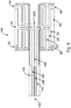
- Figure 6 shows a first layer of the power combiner/splitter of Figure 5 .
- the first layer is a "lower” layer, but the arrangement may be inverted such that the layer shown in Figure 6 is an "upper” layer.
- the layer in Figure 6 includes patterned metal features of the branched arrangements form the paths of both the first and the second combiner/splitters of the power combiner/splitter 100.
- a first stage 140 of the second combiner/splitter is present, as is the second stage 50 of the first combiner/splitter.
- Each stage 140, 50 includes patterned metal features defined in the lower layer of the metallisation stack.
- the first stage 140 of the second combiner/splitter includes a signal line 148 and two ground lines 142, 144 which are arranged on either side of the signal line 148.
- the signal line bifurcates, and each bifurcated path leads onto respective parts of the second stage 150 of the second combiner/splitter (see Figure 8 ).
- a further ground line 146 is positioned between the two bifurcated paths of the signal line 148.
- the ground lines 142, 144, 146 collectively act to improve the isolation of the signal line 148, to inhibit cross talk with other features in the stack, such as the patterned metal features forming the first combiner/splitter.
- the second stage 50 of the first combiner/splitter in this embodiment has two parts provided on opposite sides of the power combiner/splitter 100. Each part may be arranged as a mirror image of the other part, as shown in Figure 6 . Each part includes a signal line 58. Note that the signal line 58 in each part of the second stage 50 is bifurcated, with one path of the bifurcated signal line leading to/from the port 36 (or the port 32) and the other leading to/from the port 38 (or the port 34). Each part of the second stage also includes ground lines 52, 54. The ground lines 52, 54 are located on either side of the signal line 58, to improve the isolation of the signal line 58. Note that in the present embodiment the ground line 52 may be coupled to the ground line 144.
- the area 200 includes features for coupling the various patterned metal features of the lower layer of the stack with features in other layers of the stack. These features with be described below in relation to Figures 9 and 10 .
- Figure 7 shows an intermediate layer of the power combiner/splitter of Figure 5 .
- the intermediate layer is located in between the first layer shown in Figure 6 and the further layer to be described below in relation to Figure 8 .
- the underlying features of the lower layer described above in relation to Figure 6 may also be seen in Figure 7 .
- the intermediate layer in this embodiment includes patterned metal features forming a ground plane 70.
- the ground plane 70 is thus located in between the patterned metal features in the lower layer and the upper lay of the stack, thereby to improve the isolation between the first and second combiner/splitters.
- the ground plane 70 thereby forms a shared ground plane for the branched arrangements of the first and second combiner/splitters.
- the ground plane 70 in this embodiment extends to substantially cover the area (or "footprint") occupied by the features of the lower layer and the upper layer of the stack, again to improve the isolation between the first and second combiner/splitters.
- a via 80 extends though the stack to connect the ground line(s) (e.g. the ground line 146) to the ground plane 70.
- Other such vias may also be provided to connect the ground plane 70 to the other ground lines 142, 144, 52, 54 in the lower layer, as well as to the ground lines in the upper layer.
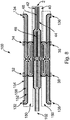
- Figure 8 shows a further layer of the power combiner/splitter of Figure 5 .
- the further layer is an "upper" layer in the stack.
- the layers in the stack may be inverted such that the layer shown in Figure 8 is a "lower” layer.
- the underlying features of the lower layer described above in relation to Figure 6 and the intermediate layer described above in relation to Figure 7 may also be seen in Figure 8 .
- the layer in Figure 8 includes patterned metal features of the branched arrangements form the paths of both the first and the second combiner/splitters of the power combiner/splitter 100.
- a second stage 150 of the second combiner/splitter is present, as is the first stage 40 of the first combiner/splitter.
- Each stage 40, 150 includes patterned metal features defined in the upper layer of the metallisation stack.
- the patterned metal features of the second stage 150 of the second combiner/splitter and the first stage 40 of the first combiner/splitter in the upper layer may be similar is some respects to the patterned metal features of the first stage 140 of the second combiner/splitter and the second stage 50 of the first combiner/splitter described above in relation to Figure 6 .
- the ports 132, 134 are laterally separated from the ports 32, 34 so that they do not overlay each other in the stack (the ports 136, 138 and the ports 36, 38 are arranged similarly), thereby improving the isolation between the various ports.
- the first stage 40 of the first combiner/splitter includes a signal line 48 and two ground lines 42, 44 which are arranged on either side of the signal line 48.
- the signal line bifurcates, and each bifurcated path leads onto respective parts of the second stage 50 of the first combiner/splitter (see Figure 6 ).
- a further ground line 46 may be positioned between the two bifurcated paths of the signal line 48.
- the ground lines 42, 44, 46 collectively act to improve the isolation of the signal line 48, to inhibit cross talk with other features in the stack, such as the patterned metal features forming the second combiner/splitter.
- the second stage 150 of the second combiner/splitter in this embodiment has two parts provided on opposite sides of the power combiner/splitter 100. These opposite sides may correspond to the sides of the power combiner/splitter 100 in which the two parts of the second stage 50 of the first combiner/splitter are located. The two parts of each second stage 50, 150 in the stack may therefore overlap to some extent. As described above, the ground plane 70 may be located in between these parts, so as to improve the isolation between them.
- Each part of the second stage 150 may be arranged as a mirror image of the other part, as shown in Figure 8 .
- Each part includes a signal line 158.
- the signal line 158 in each part of the second stage 150 is bifurcated, with one path of the bifurcated signal line leading to/from the port 136 (or the port 132) and the other leading to/from the port 138 (or the port 134).
- Each part of the second stage 150 also includes ground lines 152, 154.
- the ground lines 152, 154 are located on either side of the signal line 158, to improve the isolation of the signal line 158. Note that in the present embodiment the ground line 152 may be coupled to the ground line 42.
- Figures 9 and 10 show a detail of the power combiner/splitter, corresponding to the area 200 shown in Figure 6 .
- Figure 10 shows the same arrangement with the inclusion of the ground plane 70.
- the layout shown in Figure 6 has another area neighboring to the area 200, which may have a similar layout (e.g. mirror image of) the layout shown in Figure 9 .
- the area 200 in Figure 9 includes an end of the signal line 148 of the first stage 140 of the second combiner/splitter and its connection through the stack to the signal line 158 of the second stage 150 of the second combiner/splitter by a via 82, which extends vertically through the stack between the lower layer and the upper layer.
- the area 200 in Figure 9 also includes an end of the signal line 48 of the first stage 40 of the first combiner/splitter and its connection through the stack to the signal line 58 of the second stage 50 of the first combiner/splitter by a pair of vias 82, which again extend vertically through the stack between the lower layer and the upper layer.
- the parts of the signal lines 58, 158 shown in Figure 9 overlap and there are also a number of cross over points between the lines of the upper and lower layers shown in Figure 9 .
- the ground plane 70 described herein may serve to improve the isolation of these parts of the combiner/splitters at those points.
- the ground plane 70 may be provided with openings 72, 74 to allow one or more of the vias 82 to extend between the upper and lower layers of the stack, so as to interconnect the patterned metal features in those layers with each other without shorting at the ground plane 70.
- the openings 74 may generally conform with the footprint of one (e.g. at 72) or a collection (e.g. at 74) of vias 82. This can allow the openings 72, 74 to be made relatively small for improving the isolation provided by the ground plane 70 at the interface between the first and second stage of each combiner/splitter.
- Figure 11 shows a power combiner/splitter 100 of the kind described above provided on a surface of a semiconductor substate 300 according to an embodiment of this disclosure.
- the substrate 300 be a semiconductor die of an integrated circuit.
- the metallisation stack 202 implementing the power combiner/splitter 100 may be provided on some other kind of surface, such as the surface of a printed circuit board (PCB).
- the metallisation stack has four layers 204, 206, 208, 210. These layers 204, 206, 208, 210 may for instance correspond to layers Cu1, Cu2, Cu3, Cu4 in a metallisation stack.
- dielectric layers may be provided in between the layers 204, 206, 208, 210 and vias may extend through the dielectric layers so as to interconnect patterned metal features in the different metal layers 204, 206, 208, 210. Again, dielectric may also be present within the "metal" layers, to fill the areas not occupied by the patterned metal features.
- metal posts 212 may extend from the stack 202 toward the substrate 300. These posts 212 may, for instance, be connected to the various ports of the combiner/splitters located in the stack 202.
- a method of making a power combiner/splitter of the kind described above may be provided.
- Standard back-end-of-line processing techniques may be used to form the metallisation stack and the various features of the combiner/splitters.
- the method may include forming a metallisation stack formed on a surface (e.g. that of the substrate 300 shown in Figure 11 .
- the metallisation stack may include a plurality of layers including patterned metal features (e.g. as described above in relation to Figures 5 to 10 ).
- the patterned metal features may form a first branched arrangement (e.g. see the stages 40, 50 described above in relation to Figures 6 and 8 ) having a first port located at one end of the first branched arrangement.
- the first branched arrangement may also have a plurality of further ports located at another end of the first branched arrangement.
- the first branched arrangement may further include a plurality of bifurcated branches extending between each end of the first branched arrangement for dividing/combining a signal passing through the first branched arrangement between the first port and the plurality of further ports of the first branched arrangement.
- the patterned metal features may also form a second branched arrangement (e.g. see the stages 140, 150 described above in relation to Figures 6 and 8 ).
- the second branched arrangement may have a first port located at one end of the second branched arrangement.
- the second branched arrangement may also have a plurality of further ports located at another end of the second branched arrangement.
- the first branched arrangement may further include a plurality of bifurcated branches extending between each end of the second branched arrangement for dividing/combining a signal passing through the second branched arrangement between the first port and the plurality of further ports of the second branched arrangement.
- the first branched arrangement and the second branched arrangement may be located in a common area of the metallisation stack such that at least some of the patterned metal features forming the first branched arrangement overlie at least some of the patterned metal features forming the second branched arrangement.
- the method may further include forming a common ground plane in a layer of the metallisation stack (e.g. as described above in relation to Figure 7 .
- the common ground plane may be shared by the first and second branched arrangements.
- FIG. 5 A review of Figures 5 to 9 shows that the layout of the power combiner/splitter 100 may in some embodiments have at least one plane of symmetry. This can improve the operation of the power combiner/splitter 100 by reducing phase imbalance and phase insertion between the different paths in the power combiner/splitter 100.
- the power combiner/splitter 100 has two planes of symmetry 400, 500, which are orthogonal to each other as shown in Figure 5 .
- a metallisation stack has a plurality of layers including patterned metal features forming first and second branched arrangements of the power combiner/splitter.
- Each branched arrangement includes a port located at one end of that branched arrangement, and a plurality of further ports.
- Each branched arrangement also includes a plurality of bifurcated branches extending between each end of that branched arrangement for dividing/combining a signal passing through that branched arrangement between the port and the plurality of further ports.
- the metallisation stack further includes a common ground plane that is shared by the first and second branched arrangements. At least some of the patterned metal features forming the first branched arrangement overlie at least some of the patterned metal features forming the second branched arrangement.
Landscapes
- Engineering & Computer Science (AREA)
- Manufacturing & Machinery (AREA)
- Semiconductor Integrated Circuits (AREA)
- Design And Manufacture Of Integrated Circuits (AREA)
Abstract
Description
- The present specification relates to a power combiner/splitter of the kind that may be used in millimetre wave (mm-Wave) applications requiring Multiple-Input and Multiple-Output (MIMO) operation.
- The Wilkinson combiner/splitter a popular device for mmWave design. Although the implementation of a Wilkinson combiner/splitter can be generally straightforward, it can typically consume a lot of area on the substrate. Despite this, with the increasing demand for mm-Wave integrated circuits (ICs), this type of device can be integrated on silicon and/or laminate types of structure.
- For analog beamforming (phased-array operation), there is strong requirement to provide a dual polarization patch antenna allowing MIMO operation. As a consequence, two Wilkinson combiners have to be integrated.
- Aspects of the present disclosure are set out in the accompanying independent and dependent claims. Combinations of features from the dependent claims may be combined with features of the independent claims as appropriate and not merely as explicitly set out in the claims.
- According to an aspect of the present disclosure, there is provided a power combiner/splitter for multiple input multiple output (MIMO) applications, the power combiner/splitter comprising:
a metallisation stack formed on a surface, the metallisation stack comprising a plurality of layers including patterned metal features, the patterned metal features forming:
a first branched arrangement comprising: - a first port located at one end of the first branched arrangement;
- a plurality of further ports located;
- a plurality of bifurcated branches extending between the first port of the first branched arrangement and the plurality of further ports of the first branched arrangement for dividing/combining a signal passing through the first branched arrangement between the first port and the plurality of further ports of the first branched arrangement; and a second branched arrangement comprising:
- a first port located at one end of the second branched arrangement;
- a plurality of further ports;
- a plurality of bifurcated branches extending between the first port of the second branched arrangement and the plurality of further ports of the first branched arrangement for dividing/combining a signal passing through the second branched arrangement between the first port and the plurality of further ports of the second branched arrangement;
- According to another aspect of the present disclosure, there is provided a method of making a power combiner/splitter for multiple input multiple output (MIMO) applications, the method comprising:
- forming a metallisation stack formed on a surface, the metallisation stack comprising a plurality of layers including patterned metal features, the patterned metal features forming:
- a first branched arrangement comprising:
- a first port located at one end of the first branched arrangement;
- a plurality of further ports located;
- a plurality of bifurcated branches extending between the first port of the first branched arrangement and the plurality of further ports of the first branched arrangement for dividing/combining a signal passing through the first branched arrangement between the first port and the plurality of further ports of the first branched arrangement; and a second branched arrangement comprising:
- a first port located at one end of the second branched arrangement;
- a plurality of further ports;
- a plurality of bifurcated branches extending between the first port of the second branched arrangement and the plurality of further ports of the first branched arrangement for dividing/combining a signal passing through the second branched arrangement between the first port and the plurality of further ports of the second branched arrangement;
- wherein the first branched arrangement and the second branched arrangement are located in a common area of the metallisation stack such that at least some of the patterned metal features forming the first branched arrangement overlie at least some of the patterned metal features forming the second branched arrangement; and
- a first branched arrangement comprising:
- forming a common ground plane in a layer of the metallisation stack, wherein the common ground plane is shared by the first and second branched arrangements.
- The provision of the features of a combiner/splitter in a metallisation stack allows for improved manufacturing including convenient scaling of the device (e.g. choice of number of inputs/outputs for MIMO applications) and further allows the combiner/splitter to be integrated e.g. on a die of a semiconductor die using back end of line (BEOL) processing techniques. The metallisation stack implementation allows for the provision and selective placement of a common ground plane layer for optimised isolation between the first and second branched arrangements.
- In some embodiments, the first port of the first branched arrangement is an input and the plurality of further ports of the first branched arrangement are outputs. In some other embodiments, the first port of the first branched arrangement is an output and the plurality of further ports of the first branched arrangement are inputs.
- In some embodiments, the first port of the second branched arrangement is an input and the plurality of further ports of the second branched arrangement are outputs. In some other embodiments, the first port of the second branched arrangement is an output and the plurality of further ports of the second branched arrangement are inputs.
- Accordingly, the power combiner/splitter can act as a power combiner or a power splitter according to the configuration of the ports as inputs/outputs.
- In some embodiments, the first port of the first branched arrangement and the first port of the second branched arrangement are located at the same end of the power combiner/splitter. In some other embodiments, the first port of the first branched arrangement and the first port of the second branched arrangement are located at opposite ends of the power combiner/splitter.
- In some other embodiments, the patterned metal features forming at least some of the branches of the first branched arrangement are formed in a same layer of the metallisation stack as the patterned metal features forming at least some of the branches of the second branched arrangement.
- In some other embodiments, the patterned metal features forming the first branched arrangement are located in a plurality of layers of the metallisation stack. In some other embodiments, the patterned metal features forming the second branched arrangement are located in a plurality of layers of the metallisation stack. In some other embodiments, the metallisation stack includes two layers each including patterned metal features forming at least some of the branches of the first branched arrangement and patterned metal features forming at least some of the branches of the second branched arrangement.
- In some other embodiments, a first of the two layers includes:
- patterned metal features forming branches of the first branched arrangement proximal the first port of the first branched arrangement; and
- patterned metal features forming branches of the second branched arrangement proximal said plurality of further ports of the second branched arrangement; and
- a second of the two layers includes:
- patterned metal features forming branches of the first branched arrangement proximal said plurality of further ports of the first branched arrangement; and
- patterned metal features forming branches of the second branched arrangement proximal the first port of the second branched arrangement.
- In some other embodiments, the ground plane is located in a layer located in-between said two layers. This can improve the isolation between the first and second branched arrangements.
- In some other embodiments, all of the patterned metal features forming the first branched arrangement are located in a first layer of the metallisation stack and all of the patterned metal features forming the second branched arrangement are located in a second layer of the metallisation stack. The ground plane can be located in a layer of the metallisation stack located in-between the first layer and the second layer. This can improve the isolation between the first and second branched arrangements.
- According to a further aspect of the present disclosure, there is provided an integrated circuit comprising the power combiner/splitter of any of claims 1 to 12, wherein the metallisation stack is formed on a surface of a semiconductor die of the integrated circuit.
- According to another aspect of the present disclosure, there is provided a carrier for a semiconductor device, the carrier comprising the power combiner/splitter of any of claims 1 to 12, wherein the metallisation stack is formed on a surface of the carrier.
- Embodiments of this disclosure will be described hereinafter, by way of example only, with reference to the accompanying drawings in which like reference signs relate to like elements and in which:
-
Figure 1 schematically illustrates a Wilkinson combiner/splitter; -
Figure 2 schematically illustrates a cascaded Wilkinson combiner/splitter; -
Figure 3 schematically illustrates a power combiner/splitter according to an embodiment of this disclosure; -
Figure 4 schematically illustrates a power combiner/splitter according to another embodiment of this disclosure; -
Figure 5 shows a power combiner/splitter according to a further embodiment of this disclosure; -
Figure 6 shows a lower layer of the power combiner/splitter ofFigure 5 ; -
Figure 7 shows an intermediate layer of the power combiner/splitter ofFigure 5 ; -
Figure 8 shows an upper layer of the power combiner/splitter ofFigure 5 ; -
Figures 9 and 10 show a detail of the power combiner/splitter ofFigure 5 ; and -
Figure 11 shows a power combiner/splitter provided on a semiconductor substate according to an embodiment of this disclosure; - Embodiments of this disclosure are described in the following with reference to the accompanying drawings.
-
Figure 1 schematically illustrates an example of a Wilkinson combiner/splitter 10. The combiner/splitter 10 has afirst port 2, asecond port 14 and athird port 16. When operating as a splitter, thefirst port 2 may act as an input port and theports first port 2 may act as an output port and theports splitter 10 has two λ/4lines splitter 10 acts as a splitter, a signal input atport 2 is split into two equivalent paths along thelines - Although the Wilkinson combiner/
splitter 10 shown inFigure 1 has twoports splitter 10 may be expanded (in a cascaded configuration) to have more ports of this kind. Thus,Figure 2 schematically illustrates another example of a Wilkinson combiner/splitter 10. In the example ofFigure 2 , the combiner/splitter 10 hasports first port 2 may act as an input port and theports first port 2 may act as an output port and theports splitter 10 shown inFigure 2 may be considered to comprise a combiner/splitter 10 of the kind shown inFigure 1 , with two further such combiner/splitters 10 coupled to theports Figure 1 . When, for example, the combiner/splitter 10 acts as a splitter, a signal input atport 2 is split into four equivalent paths along thelines splitter 10 shown inFigure 1 may allow for even more combiner inputs or splitter outputs to be provided. - Wilkinson combiner/splitters may occupy a relatively large area, which may be problematic when. For instance, more than one such combiner/splitter is provided on a substrate such as a semiconductor substrate or other carrier, where space may be at a premium. In accordance with embodiments of this disclosure, a plurality of combiner/splitters may be provided in a metallisation stack (e.g. on a surface of semiconductor substrate or carrier) in an stacked arrangement in which features of each combiner/splitters overlay each other.
-
Figure 3 schematically illustrates a power combiner/splitter 100 according to an embodiment of this disclosure. In this embodiment, a first combiner/splitter hasports Figure 2 . In this embodiment, a second combiner/splitter hasports Figure 2 . Embodiments of this disclosure may facilitate multiple input multiple output (MIMO) applications by providing multiple such ports. - The impedances between the
ports Figure 3 by theimpendances ports Figure 3 by theimpendences Figure 3 , the first combiner/splitter overlays the second combiner/splitter, and the first combiner/splitter has an opposite orientation to the second combiner/splitter, such that theport 2 of the first combiner/splitter is provided on the same side of the power combiner/splitter 100 as theports port 102 of the second combiner/splitter is provided on the same side of the power combiner/splitter 100 as theports -
Figure 4 schematically illustrates a power combiner/splitter 100 according to another embodiment of this disclosure. As with the embodiment ofFigure 3 , the power combiner/splitter 100 in this embodiment comprises a first combiner/splitter which overlays the second combiner/splitter. However, in this embodiment, both combiner/splitters in the power combiner/splitter 100 have the same orientation so that theport 2 of the first combiner/splitter is provided on the same side of the power combiner/splitter 100 as theport 102 of the second combiner/splitter and such that theports splitter 100 as theports - The combiner/splitters in
Figure 3 and 4 may include further cascading of the kind noted above in relation toFigure 2 , thereby to increase the number of ports. - When combiner/splitters are overlaid in the manner shown in
Figures 3 or 4 , isolation between the paths of the combiner/splitters may become problematic. For instance, cross talk may occur at points such as thepoints Figures 3 and 4 , where branching points of the paths within each combiner/splitter overlap. - In accordance with embodiments of this disclosure, the features of a power combiner/splitter may be incorporated in a metallisation stack. The design flexibility afforded by implementing the power combiner/splitter in a metallisation stack may allow for easy scaling (cascading) of the combiner/splitters and may also allow for steps to be taken to improve isolation between the various paths of overlying combiner/splitters.
- A power combiner/
splitter 100 according to a further embodiment of this disclosure will now be described with reference toFigures 5 to 10 . - An overview of the power combiner/
splitter 100 is shown inFigure 5 . The power combiner/splitter 100 in this embodiment has a first combiner/splitter having ports splitter having ports Figures 3 and 4 . The overall topology of the power combiner/splitter 100 inFigure 5 is similar to that shown inFigure 3 in the sense that theports splitter 100, however embodiments having topologies similar to that shown inFigure 4 may be implemented, in which theports splitter 100. Note that theports ports splitter 100 inFigure 5 , as are theports ports - As described herein, the features (paths/ports) of the power combiner/
splitter 100 inFigure 5 are implemented using a plurality of metal layers in a metallisation stack. Each metal layer in the stack includes patterned metal features defining the paths, ports, etc. of the first and second combiner/splitters. Dielectric layers may be provided in between the layers and vias may extend through the dielectric layers so as to interconnect patterned metal features in the different metal layers. Dielectric may also be present within the "metal" layers, to fill the areas not occupied by the patterned metal features. As will be described below in relation toFigure 11 , the metallisation stack may be located on a surface such as the surface of a semiconductor substrate or other carrier (e.g. a printed circuit board (PCB)). -
Figure 6 shows a first layer of the power combiner/splitter ofFigure 5 . In this embodiment, the first layer is a "lower" layer, but the arrangement may be inverted such that the layer shown inFigure 6 is an "upper" layer. - The layer in
Figure 6 includes patterned metal features of the branched arrangements form the paths of both the first and the second combiner/splitters of the power combiner/splitter 100. In particular, afirst stage 140 of the second combiner/splitter is present, as is thesecond stage 50 of the first combiner/splitter. Eachstage - In particular, in this embodiment, the
first stage 140 of the second combiner/splitter includes asignal line 148 and twoground lines 142, 144 which are arranged on either side of thesignal line 148. Note that the signal line bifurcates, and each bifurcated path leads onto respective parts of thesecond stage 150 of the second combiner/splitter (seeFigure 8 ). Afurther ground line 146 is positioned between the two bifurcated paths of thesignal line 148. The ground lines 142, 144, 146 collectively act to improve the isolation of thesignal line 148, to inhibit cross talk with other features in the stack, such as the patterned metal features forming the first combiner/splitter. - The
second stage 50 of the first combiner/splitter in this embodiment has two parts provided on opposite sides of the power combiner/splitter 100. Each part may be arranged as a mirror image of the other part, as shown inFigure 6 . Each part includes asignal line 58. Note that thesignal line 58 in each part of thesecond stage 50 is bifurcated, with one path of the bifurcated signal line leading to/from the port 36 (or the port 32) and the other leading to/from the port 38 (or the port 34). Each part of the second stage also includesground lines signal line 58, to improve the isolation of thesignal line 58. Note that in the present embodiment theground line 52 may be coupled to theground line 144. - The
area 200 includes features for coupling the various patterned metal features of the lower layer of the stack with features in other layers of the stack. These features with be described below in relation toFigures 9 and 10 . -
Figure 7 shows an intermediate layer of the power combiner/splitter ofFigure 5 . The intermediate layer is located in between the first layer shown inFigure 6 and the further layer to be described below in relation toFigure 8 . The underlying features of the lower layer described above in relation toFigure 6 may also be seen inFigure 7 . - The intermediate layer in this embodiment includes patterned metal features forming a
ground plane 70. Theground plane 70 is thus located in between the patterned metal features in the lower layer and the upper lay of the stack, thereby to improve the isolation between the first and second combiner/splitters. Theground plane 70 thereby forms a shared ground plane for the branched arrangements of the first and second combiner/splitters. Theground plane 70 in this embodiment extends to substantially cover the area (or "footprint") occupied by the features of the lower layer and the upper layer of the stack, again to improve the isolation between the first and second combiner/splitters. - In this embodiment, a via 80 extends though the stack to connect the ground line(s) (e.g. the ground line 146) to the
ground plane 70. Other such vias may also be provided to connect theground plane 70 to theother ground lines -
Figure 8 shows a further layer of the power combiner/splitter ofFigure 5 . In this embodiment, the further layer is an "upper" layer in the stack. However, as noted above, the layers in the stack may be inverted such that the layer shown inFigure 8 is a "lower" layer. The underlying features of the lower layer described above in relation toFigure 6 and the intermediate layer described above in relation toFigure 7 may also be seen inFigure 8 . - The layer in
Figure 8 includes patterned metal features of the branched arrangements form the paths of both the first and the second combiner/splitters of the power combiner/splitter 100. In particular, asecond stage 150 of the second combiner/splitter is present, as is thefirst stage 40 of the first combiner/splitter. Eachstage - As will be appreciated from the description below, the patterned metal features of the
second stage 150 of the second combiner/splitter and thefirst stage 40 of the first combiner/splitter in the upper layer may be similar is some respects to the patterned metal features of thefirst stage 140 of the second combiner/splitter and thesecond stage 50 of the first combiner/splitter described above in relation toFigure 6 . Note that in this embodiment however, theports ports ports ports - In this embodiment, the
first stage 40 of the first combiner/splitter includes asignal line 48 and twoground lines signal line 48. Note that the signal line bifurcates, and each bifurcated path leads onto respective parts of thesecond stage 50 of the first combiner/splitter (seeFigure 6 ). Afurther ground line 46 may be positioned between the two bifurcated paths of thesignal line 48. The ground lines 42, 44, 46 collectively act to improve the isolation of thesignal line 48, to inhibit cross talk with other features in the stack, such as the patterned metal features forming the second combiner/splitter. - The
second stage 150 of the second combiner/splitter in this embodiment has two parts provided on opposite sides of the power combiner/splitter 100. These opposite sides may correspond to the sides of the power combiner/splitter 100 in which the two parts of thesecond stage 50 of the first combiner/splitter are located. The two parts of eachsecond stage ground plane 70 may be located in between these parts, so as to improve the isolation between them. - Each part of the
second stage 150 may be arranged as a mirror image of the other part, as shown inFigure 8 . Each part includes asignal line 158. Note that thesignal line 158 in each part of thesecond stage 150 is bifurcated, with one path of the bifurcated signal line leading to/from the port 136 (or the port 132) and the other leading to/from the port 138 (or the port 134). Each part of thesecond stage 150 also includesground lines signal line 158, to improve the isolation of thesignal line 158. Note that in the present embodiment theground line 152 may be coupled to theground line 42. -
Figures 9 and 10 show a detail of the power combiner/splitter, corresponding to thearea 200 shown inFigure 6 . In particular, while patterned metal features of the upper and lower layers can be seen inFigure 9, Figure 10 shows the same arrangement with the inclusion of theground plane 70. Note also that the layout shown inFigure 6 has another area neighboring to thearea 200, which may have a similar layout (e.g. mirror image of) the layout shown inFigure 9 . - The
area 200 inFigure 9 includes an end of thesignal line 148 of thefirst stage 140 of the second combiner/splitter and its connection through the stack to thesignal line 158 of thesecond stage 150 of the second combiner/splitter by a via 82, which extends vertically through the stack between the lower layer and the upper layer. - The
area 200 inFigure 9 also includes an end of thesignal line 48 of thefirst stage 40 of the first combiner/splitter and its connection through the stack to thesignal line 58 of thesecond stage 50 of the first combiner/splitter by a pair ofvias 82, which again extend vertically through the stack between the lower layer and the upper layer. - Note that the parts of the signal lines 58, 158 shown in
Figure 9 overlap and there are also a number of cross over points between the lines of the upper and lower layers shown inFigure 9 . Again, theground plane 70 described herein may serve to improve the isolation of these parts of the combiner/splitters at those points. - As can be seen in
Figure 10 , theground plane 70 may be provided withopenings ground plane 70. Theopenings 74 may generally conform with the footprint of one (e.g. at 72) or a collection (e.g. at 74) ofvias 82. This can allow theopenings ground plane 70 at the interface between the first and second stage of each combiner/splitter. -
Figure 11 shows a power combiner/splitter 100 of the kind described above provided on a surface of asemiconductor substate 300 according to an embodiment of this disclosure. Thesubstrate 300 be a semiconductor die of an integrated circuit. As described previously, themetallisation stack 202 implementing the power combiner/splitter 100 may be provided on some other kind of surface, such as the surface of a printed circuit board (PCB). InFigure 11 , the metallisation stack has fourlayers layers layers different metal layers - To provide electrical connections between the
stack 202 and thesubstrate 300, metal (e.g. Cu) posts 212 may extend from thestack 202 toward thesubstrate 300. Theseposts 212 may, for instance, be connected to the various ports of the combiner/splitters located in thestack 202. - According to embodiments of this disclosure, a method of making a power combiner/splitter of the kind described above may be provided. Standard back-end-of-line processing techniques may be used to form the metallisation stack and the various features of the combiner/splitters.
- The method may include forming a metallisation stack formed on a surface (e.g. that of the
substrate 300 shown inFigure 11 . The metallisation stack may include a plurality of layers including patterned metal features (e.g. as described above in relation toFigures 5 to 10 ). - The patterned metal features may form a first branched arrangement (e.g. see the
stages Figures 6 and8 ) having a first port located at one end of the first branched arrangement. The first branched arrangement may also have a plurality of further ports located at another end of the first branched arrangement. The first branched arrangement may further include a plurality of bifurcated branches extending between each end of the first branched arrangement for dividing/combining a signal passing through the first branched arrangement between the first port and the plurality of further ports of the first branched arrangement. - The patterned metal features may also form a second branched arrangement (e.g. see the
stages Figures 6 and8 ). The second branched arrangement may have a first port located at one end of the second branched arrangement. The second branched arrangement may also have a plurality of further ports located at another end of the second branched arrangement. The first branched arrangement may further include a plurality of bifurcated branches extending between each end of the second branched arrangement for dividing/combining a signal passing through the second branched arrangement between the first port and the plurality of further ports of the second branched arrangement. - The first branched arrangement and the second branched arrangement may be located in a common area of the metallisation stack such that at least some of the patterned metal features forming the first branched arrangement overlie at least some of the patterned metal features forming the second branched arrangement.
- The method may further include forming a common ground plane in a layer of the metallisation stack (e.g. as described above in relation to
Figure 7 . The common ground plane may be shared by the first and second branched arrangements. - A review of
Figures 5 to 9 shows that the layout of the power combiner/splitter 100 may in some embodiments have at least one plane of symmetry. This can improve the operation of the power combiner/splitter 100 by reducing phase imbalance and phase insertion between the different paths in the power combiner/splitter 100. For instance, in the embodiment ofFigures 5 to 9 , the power combiner/splitter 100 has two planes ofsymmetry Figure 5 . - Accordingly, there has been described a power combiner/splitter for multiple input multiple output (MIMO) applications and a method of making the same. A metallisation stack has a plurality of layers including patterned metal features forming first and second branched arrangements of the power combiner/splitter. Each branched arrangement includes a port located at one end of that branched arrangement, and a plurality of further ports. Each branched arrangement also includes a plurality of bifurcated branches extending between each end of that branched arrangement for dividing/combining a signal passing through that branched arrangement between the port and the plurality of further ports. The metallisation stack further includes a common ground plane that is shared by the first and second branched arrangements. At least some of the patterned metal features forming the first branched arrangement overlie at least some of the patterned metal features forming the second branched arrangement.
- Although particular embodiments of this disclosure have been described, it will be appreciated that many modifications/additions and/or substitutions may be made within the scope of the claims.
wherein the first branched arrangement and the second branched arrangement are located in a common area of the metallisation stack such that at least some of the patterned metal features forming the first branched arrangement overlie at least some of the patterned metal features forming the second branched arrangement.
Claims (15)
- A power combiner/splitter for multiple input multiple output (MIMO) applications, the power combiner/splitter comprising:
a metallisation stack formed on a surface, the metallisation stack comprising a plurality of layers including patterned metal features, the patterned metal features forming:a first branched arrangement comprising:a first port located at one end of the first branched arrangement;a plurality of further ports located;a plurality of bifurcated branches extending between the first port of the first branched arrangement and the plurality of further ports of the first branched arrangement for dividing/combining a signal passing through the first branched arrangement between the first port and the plurality of further ports of the first branched arrangement; anda second branched arrangement comprising:wherein the metallisation stack further comprises a common ground plane shared by the first and second branched arrangements, anda first port located at one end of the second branched arrangement;a plurality of further ports;a plurality of bifurcated branches extending between the first port of the second branched arrangement and the plurality of further ports of the first branched arrangement for dividing/combining a signal passing through the second branched arrangement between the first port and the plurality of further ports of the second branched arrangement;
wherein the first branched arrangement and the second branched arrangement are located in a common area of the metallisation stack such that at least some of the patterned metal features forming the first branched arrangement overlie at least some of the patterned metal features forming the second branched arrangement. - The power combiner/splitter of claim 1, wherein:the first port of the first branched arrangement is an input and the plurality of further ports of the first branched arrangement are outputs; orthe first port of the first branched arrangement is an output and the plurality of further ports of the first branched arrangement are inputs.
- The power combiner/splitter of claim 1 or claim 2, wherein:the first port of the second branched arrangement is an input and the plurality of further ports of the second branched arrangement are outputs; orthe first port of the second branched arrangement is an output and the plurality of further ports of the second branched arrangement are inputs.
- The power combiner/splitter of any preceding claim, wherein the first port of the first branched arrangement and the first port of the second branched arrangement are located at the same end of the power combiner/splitter.
- The power combiner/splitter of any of claims 1 to 3, wherein the first port of the first branched arrangement and the first port of the second branched arrangement are located at opposite ends of the power combiner/splitter.
- The power combiner/splitter of any preceding claim, wherein the patterned metal features forming at least some of the branches of the first branched arrangement are formed in a same layer of the metallisation stack as the patterned metal features forming at least some of the branches of the second branched arrangement.
- The power combiner/splitter of claim 6, wherein the patterned metal features forming the first branched arrangement are located in a plurality of layers of the metallisation stack.
- The power combiner/splitter of claim 6 or claim 7, wherein the patterned metal features forming the second branched arrangement are located in a plurality of layers of the metallisation stack.
- The power combiner/splitter of claim 7 or claim 8, wherein the metallisation stack includes two layers each including patterned metal features forming at least some of the branches of the first branched arrangement and patterned metal features forming at least some of the branches of the second branched arrangement.
- The power combiner/splitter of claim 9, wherein:a first of said two layers includes:patterned metal features forming branches of the first branched arrangement proximal the first port of the first branched arrangement; andpatterned metal features forming branches of the second branched arrangement proximal said plurality of further ports of the second branched arrangement; anda second of said two layers includes:patterned metal features forming branches of the first branched arrangement proximal said plurality of further ports of the first branched arrangement; andpatterned metal features forming branches of the second branched arrangement proximal said first port of the second branched arrangement.
- The power combiner/splitter of claim 9 or claim 10, wherein the ground plane is located in a layer located in-between said two layers.
- The power combiner/splitter of any of claims 1 to 5, wherein all of the patterned metal features forming the first branched arrangement are located in a first layer of the metallisation stack, wherein all of the patterned metal features forming the second branched arrangement are located in a second layer of the metallisation stack, and wherein the ground plane is located in a layer of the metallisation stack located in-between the first layer and the second layer.
- An integrated circuit comprising the power combiner/splitter of any preceding claim, wherein the metallisation stack is formed on a surface of a semiconductor die of the integrated circuit.
- A carrier for a semiconductor device, the carrier comprising the power combiner/splitter of any of claims 1 to 12, wherein the metallisation stack is formed on a surface of the carrier.
- A method of making a power combiner/splitter for multiple input multiple output (MIMO) applications, the method comprising:forming a metallisation stack formed on a surface, the metallisation stack comprising a plurality of layers including patterned metal features, the patterned metal features forming:a first branched arrangement comprising:a first port located at one end of the first branched arrangement;a plurality of further ports located;a plurality of bifurcated branches extending between the first port of the first branched arrangement and the plurality of further ports of the first branched arrangement for dividing/combining a signal passing through the first branched arrangement between the first port and the plurality of further ports of the first branched arrangement; anda second branched arrangement comprising:wherein the first branched arrangement and the second branched arrangement are located in a common area of the metallisation stack such that at least some of the patterned metal features forming the first branched arrangement overlie at least some of the patterned metal features forming the second branched arrangement; anda first port located at one end of the second branched arrangement;a plurality of further ports;a plurality of bifurcated branches extending between the first port of the second branched arrangement and the plurality of further ports of the first branched arrangement for dividing/combining a signal passing through the second branched arrangement between the first port and the plurality of further ports of the second branched arrangement;forming a common ground plane in a layer of the metallisation stack, wherein the common ground plane is shared by the first and second branched arrangements.
Priority Applications (3)
| Application Number | Priority Date | Filing Date | Title |
|---|---|---|---|
| EP20305497.8A EP3910732B1 (en) | 2020-05-14 | 2020-05-14 | Power combiner/splitter for millimetre wave applications |
| US17/314,219 US12009565B2 (en) | 2020-05-14 | 2021-05-07 | Power combiner/splitter for millimetre wave applications |
| CN202110519509.7A CN113675571B (en) | 2020-05-14 | 2021-05-08 | Power combiners/splitters for millimeter-wave applications |
Applications Claiming Priority (1)
| Application Number | Priority Date | Filing Date | Title |
|---|---|---|---|
| EP20305497.8A EP3910732B1 (en) | 2020-05-14 | 2020-05-14 | Power combiner/splitter for millimetre wave applications |
Publications (2)
| Publication Number | Publication Date |
|---|---|
| EP3910732A1 true EP3910732A1 (en) | 2021-11-17 |
| EP3910732B1 EP3910732B1 (en) | 2024-07-10 |
Family
ID=71108540
Family Applications (1)
| Application Number | Title | Priority Date | Filing Date |
|---|---|---|---|
| EP20305497.8A Active EP3910732B1 (en) | 2020-05-14 | 2020-05-14 | Power combiner/splitter for millimetre wave applications |
Country Status (3)
| Country | Link |
|---|---|
| US (1) | US12009565B2 (en) |
| EP (1) | EP3910732B1 (en) |
| CN (1) | CN113675571B (en) |
Citations (1)
| Publication number | Priority date | Publication date | Assignee | Title |
|---|---|---|---|---|
| EP0777291A2 (en) * | 1995-12-04 | 1997-06-04 | AT&T Corp. | Signal isolating microwave splitters/combiners |
Family Cites Families (14)
| Publication number | Priority date | Publication date | Assignee | Title |
|---|---|---|---|---|
| JP2000124711A (en) | 1998-10-16 | 2000-04-28 | Nippon Antenna Co Ltd | High isolation Wilkinson circuit |
| KR100863392B1 (en) | 2007-03-15 | 2008-10-14 | 순천향대학교 산학협력단 | Microstrip Transmission Line Structure and Asymmetric Wilkinson Power Divider |
| US7777570B2 (en) * | 2008-03-12 | 2010-08-17 | Mediatek Inc. | Transformer power combiner having secondary winding conductors magnetically coupled to primary winding conductors and configured in topology including series connection and parallel connection |
| WO2014063324A1 (en) * | 2012-10-25 | 2014-05-01 | Telefonaktiebolaget L M Ericsson (Publ) | Power divider and method of fabricating the same |
| CN105846032B (en) * | 2016-03-24 | 2018-04-27 | 中国计量学院 | A kind of low-loss crossing stack formula LTCC Wilkinson power dividers |
| CN106785383B (en) * | 2016-11-25 | 2019-05-07 | 电子科技大学 | A feed network layer, antenna system and method for generating four polarization modes |
| CN206364178U (en) * | 2016-12-09 | 2017-07-28 | 安徽四创电子股份有限公司 | A kind of micro-strip array antenna |
| KR102299451B1 (en) * | 2016-12-20 | 2021-09-08 | 한국전자기술연구원 | Divider/combiner with wide band characteristic |
| EP3419104B1 (en) * | 2017-06-22 | 2022-03-09 | CommScope Technologies LLC | Cellular communication systems having antenna arrays therein with enhanced half power beam width (hpbw) control |
| WO2019103899A1 (en) * | 2017-11-27 | 2019-05-31 | Skyworks Solutions, Inc. | Wideband power combiner and splitter |
| CN108183301A (en) | 2017-12-12 | 2018-06-19 | 吴云飞 | A kind of miniaturization Wilkinson power divider with low-pass filtering |
| US10593635B2 (en) * | 2018-03-27 | 2020-03-17 | Nxp B.V. | Multi-die and antenna array device |
| CN108767408B (en) | 2018-07-27 | 2023-09-19 | 辽宁普天数码股份有限公司 | An ultra-miniature Wilkinson power splitter |
| CN110012591B (en) * | 2019-04-11 | 2024-02-27 | 成都兴仁科技有限公司 | Matrix integrated device and manufacturing method |
-
2020
- 2020-05-14 EP EP20305497.8A patent/EP3910732B1/en active Active
-
2021
- 2021-05-07 US US17/314,219 patent/US12009565B2/en active Active
- 2021-05-08 CN CN202110519509.7A patent/CN113675571B/en active Active
Patent Citations (1)
| Publication number | Priority date | Publication date | Assignee | Title |
|---|---|---|---|---|
| EP0777291A2 (en) * | 1995-12-04 | 1997-06-04 | AT&T Corp. | Signal isolating microwave splitters/combiners |
Non-Patent Citations (1)
| Title |
|---|
| NAFE AHMED ET AL: "2x64 Dual-Polarized Dual-Beam Single-Aperture 28 GHz Phased Array with High Cross-Polarization Rejection for 5G Polarization MIMO", 2019 IEEE MTT-S INTERNATIONAL MICROWAVE SYMPOSIUM (IMS), IEEE, 2 June 2019 (2019-06-02), pages 484 - 487, XP033579674 * |
Also Published As
| Publication number | Publication date |
|---|---|
| EP3910732B1 (en) | 2024-07-10 |
| US12009565B2 (en) | 2024-06-11 |
| CN113675571B (en) | 2025-09-02 |
| CN113675571A (en) | 2021-11-19 |
| US20210359388A1 (en) | 2021-11-18 |
Similar Documents
| Publication | Publication Date | Title |
|---|---|---|
| US6975267B2 (en) | Low profile active electronically scanned antenna (AESA) for Ka-band radar systems | |
| JP6743995B2 (en) | Antenna module and method for manufacturing antenna module | |
| AU2020467488B2 (en) | Antenna array architecture with electrically conductive columns between substrates | |
| JP2825394B2 (en) | N-way power combiner / divider | |
| US6778037B1 (en) | Means for handling high-frequency energy | |
| US4532484A (en) | Hybrid coupler having interlaced coupling conductors | |
| JPH09191205A (en) | Signal separation microwave splitter / combiner | |
| US12009565B2 (en) | Power combiner/splitter for millimetre wave applications | |
| US8081045B1 (en) | Beamformer power divider/combiner with transmission lines distributed between MMIC and associated PC board | |
| US6437658B1 (en) | Three-level semiconductor balun and method for creating the same | |
| US20090284326A1 (en) | Balanced hybrid coupler | |
| US9584080B2 (en) | Compact microwave power amplifier circuit | |
| JP6320167B2 (en) | Wilkinson distributor and high frequency circuit | |
| EP2634859B1 (en) | Lange coupler and fabrication method | |
| CN116387787A (en) | Three-dimensional structured miniature Wilkinson power divider | |
| CN117337518A (en) | Antenna device using coplanar waveguide interconnects between RF components | |
| Jenning et al. | Miniaturized integrated butler matrix for 180 GHz chip-to-chip communication | |
| US6842631B1 (en) | Reduced-layer isolated planar beamformer | |
| EP4468342A1 (en) | Integrated circuit package | |
| US12597712B2 (en) | Transmission line arrangement for a passive component | |
| US20240071959A1 (en) | Marchand baluns in coreless package substrates | |
| US20230298988A1 (en) | Electronic device and multi-level interposer with rf sloped via and related method | |
| JP3589446B2 (en) | Power amplifier | |
| KR20240075380A (en) | Stripline gysel power divider | |
| AU2021267093A1 (en) | Three-dimensional branch line coupler |
Legal Events
| Date | Code | Title | Description |
|---|---|---|---|
| PUAI | Public reference made under article 153(3) epc to a published international application that has entered the european phase |
Free format text: ORIGINAL CODE: 0009012 |
|
| STAA | Information on the status of an ep patent application or granted ep patent |
Free format text: STATUS: THE APPLICATION HAS BEEN PUBLISHED |
|
| AK | Designated contracting states |
Kind code of ref document: A1 Designated state(s): AL AT BE BG CH CY CZ DE DK EE ES FI FR GB GR HR HU IE IS IT LI LT LU LV MC MK MT NL NO PL PT RO RS SE SI SK SM TR |
|
| B565 | Issuance of search results under rule 164(2) epc |
Effective date: 20201015 |
|
| STAA | Information on the status of an ep patent application or granted ep patent |
Free format text: STATUS: REQUEST FOR EXAMINATION WAS MADE |
|
| 17P | Request for examination filed |
Effective date: 20220517 |
|
| RBV | Designated contracting states (corrected) |
Designated state(s): AL AT BE BG CH CY CZ DE DK EE ES FI FR GB GR HR HU IE IS IT LI LT LU LV MC MK MT NL NO PL PT RO RS SE SI SK SM TR |
|
| GRAP | Despatch of communication of intention to grant a patent |
Free format text: ORIGINAL CODE: EPIDOSNIGR1 |
|
| STAA | Information on the status of an ep patent application or granted ep patent |
Free format text: STATUS: GRANT OF PATENT IS INTENDED |
|
| RIC1 | Information provided on ipc code assigned before grant |
Ipc: H01P 5/16 20060101AFI20231207BHEP |
|
| INTG | Intention to grant announced |
Effective date: 20240103 |
|
| GRAS | Grant fee paid |
Free format text: ORIGINAL CODE: EPIDOSNIGR3 |
|
| GRAA | (expected) grant |
Free format text: ORIGINAL CODE: 0009210 |
|
| STAA | Information on the status of an ep patent application or granted ep patent |
Free format text: STATUS: THE PATENT HAS BEEN GRANTED |
|
| AK | Designated contracting states |
Kind code of ref document: B1 Designated state(s): AL AT BE BG CH CY CZ DE DK EE ES FI FR GB GR HR HU IE IS IT LI LT LU LV MC MK MT NL NO PL PT RO RS SE SI SK SM TR |
|
| REG | Reference to a national code |
Ref country code: CH Ref legal event code: EP |
|
| REG | Reference to a national code |
Ref country code: DE Ref legal event code: R096 Ref document number: 602020033689 Country of ref document: DE |
|
| REG | Reference to a national code |
Ref country code: LT Ref legal event code: MG9D |
|
| REG | Reference to a national code |
Ref country code: NL Ref legal event code: MP Effective date: 20240710 |
|
| PG25 | Lapsed in a contracting state [announced via postgrant information from national office to epo] |
Ref country code: PT Free format text: LAPSE BECAUSE OF FAILURE TO SUBMIT A TRANSLATION OF THE DESCRIPTION OR TO PAY THE FEE WITHIN THE PRESCRIBED TIME-LIMIT Effective date: 20241111 |
|
| REG | Reference to a national code |
Ref country code: AT Ref legal event code: MK05 Ref document number: 1702864 Country of ref document: AT Kind code of ref document: T Effective date: 20240710 |
|
| PG25 | Lapsed in a contracting state [announced via postgrant information from national office to epo] |
Ref country code: NL Free format text: LAPSE BECAUSE OF FAILURE TO SUBMIT A TRANSLATION OF THE DESCRIPTION OR TO PAY THE FEE WITHIN THE PRESCRIBED TIME-LIMIT Effective date: 20240710 |
|
| PG25 | Lapsed in a contracting state [announced via postgrant information from national office to epo] |
Ref country code: PT Free format text: LAPSE BECAUSE OF FAILURE TO SUBMIT A TRANSLATION OF THE DESCRIPTION OR TO PAY THE FEE WITHIN THE PRESCRIBED TIME-LIMIT Effective date: 20241111 Ref country code: NL Free format text: LAPSE BECAUSE OF FAILURE TO SUBMIT A TRANSLATION OF THE DESCRIPTION OR TO PAY THE FEE WITHIN THE PRESCRIBED TIME-LIMIT Effective date: 20240710 |
|
| PG25 | Lapsed in a contracting state [announced via postgrant information from national office to epo] |
Ref country code: NO Free format text: LAPSE BECAUSE OF FAILURE TO SUBMIT A TRANSLATION OF THE DESCRIPTION OR TO PAY THE FEE WITHIN THE PRESCRIBED TIME-LIMIT Effective date: 20241010 |
|
| PG25 | Lapsed in a contracting state [announced via postgrant information from national office to epo] |
Ref country code: FI Free format text: LAPSE BECAUSE OF FAILURE TO SUBMIT A TRANSLATION OF THE DESCRIPTION OR TO PAY THE FEE WITHIN THE PRESCRIBED TIME-LIMIT Effective date: 20240710 Ref country code: GR Free format text: LAPSE BECAUSE OF FAILURE TO SUBMIT A TRANSLATION OF THE DESCRIPTION OR TO PAY THE FEE WITHIN THE PRESCRIBED TIME-LIMIT Effective date: 20241011 Ref country code: PL Free format text: LAPSE BECAUSE OF FAILURE TO SUBMIT A TRANSLATION OF THE DESCRIPTION OR TO PAY THE FEE WITHIN THE PRESCRIBED TIME-LIMIT Effective date: 20240710 |
|
| PG25 | Lapsed in a contracting state [announced via postgrant information from national office to epo] |
Ref country code: BG Free format text: LAPSE BECAUSE OF FAILURE TO SUBMIT A TRANSLATION OF THE DESCRIPTION OR TO PAY THE FEE WITHIN THE PRESCRIBED TIME-LIMIT Effective date: 20240710 |
|
| PG25 | Lapsed in a contracting state [announced via postgrant information from national office to epo] |
Ref country code: LV Free format text: LAPSE BECAUSE OF FAILURE TO SUBMIT A TRANSLATION OF THE DESCRIPTION OR TO PAY THE FEE WITHIN THE PRESCRIBED TIME-LIMIT Effective date: 20240710 |
|
| PG25 | Lapsed in a contracting state [announced via postgrant information from national office to epo] |
Ref country code: AT Free format text: LAPSE BECAUSE OF FAILURE TO SUBMIT A TRANSLATION OF THE DESCRIPTION OR TO PAY THE FEE WITHIN THE PRESCRIBED TIME-LIMIT Effective date: 20240710 Ref country code: IS Free format text: LAPSE BECAUSE OF FAILURE TO SUBMIT A TRANSLATION OF THE DESCRIPTION OR TO PAY THE FEE WITHIN THE PRESCRIBED TIME-LIMIT Effective date: 20241110 |
|
| PG25 | Lapsed in a contracting state [announced via postgrant information from national office to epo] |
Ref country code: HR Free format text: LAPSE BECAUSE OF FAILURE TO SUBMIT A TRANSLATION OF THE DESCRIPTION OR TO PAY THE FEE WITHIN THE PRESCRIBED TIME-LIMIT Effective date: 20240710 |
|
| PG25 | Lapsed in a contracting state [announced via postgrant information from national office to epo] |
Ref country code: ES Free format text: LAPSE BECAUSE OF FAILURE TO SUBMIT A TRANSLATION OF THE DESCRIPTION OR TO PAY THE FEE WITHIN THE PRESCRIBED TIME-LIMIT Effective date: 20240710 Ref country code: RS Free format text: LAPSE BECAUSE OF FAILURE TO SUBMIT A TRANSLATION OF THE DESCRIPTION OR TO PAY THE FEE WITHIN THE PRESCRIBED TIME-LIMIT Effective date: 20241010 |
|
| PG25 | Lapsed in a contracting state [announced via postgrant information from national office to epo] |
Ref country code: RS Free format text: LAPSE BECAUSE OF FAILURE TO SUBMIT A TRANSLATION OF THE DESCRIPTION OR TO PAY THE FEE WITHIN THE PRESCRIBED TIME-LIMIT Effective date: 20241010 Ref country code: PL Free format text: LAPSE BECAUSE OF FAILURE TO SUBMIT A TRANSLATION OF THE DESCRIPTION OR TO PAY THE FEE WITHIN THE PRESCRIBED TIME-LIMIT Effective date: 20240710 Ref country code: NO Free format text: LAPSE BECAUSE OF FAILURE TO SUBMIT A TRANSLATION OF THE DESCRIPTION OR TO PAY THE FEE WITHIN THE PRESCRIBED TIME-LIMIT Effective date: 20241010 Ref country code: LV Free format text: LAPSE BECAUSE OF FAILURE TO SUBMIT A TRANSLATION OF THE DESCRIPTION OR TO PAY THE FEE WITHIN THE PRESCRIBED TIME-LIMIT Effective date: 20240710 Ref country code: IS Free format text: LAPSE BECAUSE OF FAILURE TO SUBMIT A TRANSLATION OF THE DESCRIPTION OR TO PAY THE FEE WITHIN THE PRESCRIBED TIME-LIMIT Effective date: 20241110 Ref country code: HR Free format text: LAPSE BECAUSE OF FAILURE TO SUBMIT A TRANSLATION OF THE DESCRIPTION OR TO PAY THE FEE WITHIN THE PRESCRIBED TIME-LIMIT Effective date: 20240710 Ref country code: GR Free format text: LAPSE BECAUSE OF FAILURE TO SUBMIT A TRANSLATION OF THE DESCRIPTION OR TO PAY THE FEE WITHIN THE PRESCRIBED TIME-LIMIT Effective date: 20241011 Ref country code: FI Free format text: LAPSE BECAUSE OF FAILURE TO SUBMIT A TRANSLATION OF THE DESCRIPTION OR TO PAY THE FEE WITHIN THE PRESCRIBED TIME-LIMIT Effective date: 20240710 Ref country code: ES Free format text: LAPSE BECAUSE OF FAILURE TO SUBMIT A TRANSLATION OF THE DESCRIPTION OR TO PAY THE FEE WITHIN THE PRESCRIBED TIME-LIMIT Effective date: 20240710 Ref country code: BG Free format text: LAPSE BECAUSE OF FAILURE TO SUBMIT A TRANSLATION OF THE DESCRIPTION OR TO PAY THE FEE WITHIN THE PRESCRIBED TIME-LIMIT Effective date: 20240710 Ref country code: AT Free format text: LAPSE BECAUSE OF FAILURE TO SUBMIT A TRANSLATION OF THE DESCRIPTION OR TO PAY THE FEE WITHIN THE PRESCRIBED TIME-LIMIT Effective date: 20240710 |
|
| REG | Reference to a national code |
Ref country code: DE Ref legal event code: R097 Ref document number: 602020033689 Country of ref document: DE |
|
| PG25 | Lapsed in a contracting state [announced via postgrant information from national office to epo] |
Ref country code: SM Free format text: LAPSE BECAUSE OF FAILURE TO SUBMIT A TRANSLATION OF THE DESCRIPTION OR TO PAY THE FEE WITHIN THE PRESCRIBED TIME-LIMIT Effective date: 20240710 Ref country code: DK Free format text: LAPSE BECAUSE OF FAILURE TO SUBMIT A TRANSLATION OF THE DESCRIPTION OR TO PAY THE FEE WITHIN THE PRESCRIBED TIME-LIMIT Effective date: 20240710 Ref country code: RO Free format text: LAPSE BECAUSE OF FAILURE TO SUBMIT A TRANSLATION OF THE DESCRIPTION OR TO PAY THE FEE WITHIN THE PRESCRIBED TIME-LIMIT Effective date: 20240710 |
|
| PG25 | Lapsed in a contracting state [announced via postgrant information from national office to epo] |
Ref country code: EE Free format text: LAPSE BECAUSE OF FAILURE TO SUBMIT A TRANSLATION OF THE DESCRIPTION OR TO PAY THE FEE WITHIN THE PRESCRIBED TIME-LIMIT Effective date: 20240710 |
|
| PG25 | Lapsed in a contracting state [announced via postgrant information from national office to epo] |
Ref country code: CZ Free format text: LAPSE BECAUSE OF FAILURE TO SUBMIT A TRANSLATION OF THE DESCRIPTION OR TO PAY THE FEE WITHIN THE PRESCRIBED TIME-LIMIT Effective date: 20240710 |
|
| PG25 | Lapsed in a contracting state [announced via postgrant information from national office to epo] |
Ref country code: SK Free format text: LAPSE BECAUSE OF FAILURE TO SUBMIT A TRANSLATION OF THE DESCRIPTION OR TO PAY THE FEE WITHIN THE PRESCRIBED TIME-LIMIT Effective date: 20240710 Ref country code: IT Free format text: LAPSE BECAUSE OF FAILURE TO SUBMIT A TRANSLATION OF THE DESCRIPTION OR TO PAY THE FEE WITHIN THE PRESCRIBED TIME-LIMIT Effective date: 20240710 |
|
| PLBE | No opposition filed within time limit |
Free format text: ORIGINAL CODE: 0009261 |
|
| STAA | Information on the status of an ep patent application or granted ep patent |
Free format text: STATUS: NO OPPOSITION FILED WITHIN TIME LIMIT |
|
| 26N | No opposition filed |
Effective date: 20250411 |
|
| PGFP | Annual fee paid to national office [announced via postgrant information from national office to epo] |
Ref country code: DE Payment date: 20250423 Year of fee payment: 6 |
|
| PGFP | Annual fee paid to national office [announced via postgrant information from national office to epo] |
Ref country code: FR Payment date: 20250423 Year of fee payment: 6 |
|
| P01 | Opt-out of the competence of the unified patent court (upc) registered |
Free format text: CASE NUMBER: APP_29889/2025 Effective date: 20250623 |
|
| PG25 | Lapsed in a contracting state [announced via postgrant information from national office to epo] |
Ref country code: SE Free format text: LAPSE BECAUSE OF FAILURE TO SUBMIT A TRANSLATION OF THE DESCRIPTION OR TO PAY THE FEE WITHIN THE PRESCRIBED TIME-LIMIT Effective date: 20240710 |
|
| REG | Reference to a national code |
Ref country code: CH Ref legal event code: H13 Free format text: ST27 STATUS EVENT CODE: U-0-0-H10-H13 (AS PROVIDED BY THE NATIONAL OFFICE) Effective date: 20251223 |
|
| PG25 | Lapsed in a contracting state [announced via postgrant information from national office to epo] |
Ref country code: LU Free format text: LAPSE BECAUSE OF NON-PAYMENT OF DUE FEES Effective date: 20250514 |
|
| PG25 | Lapsed in a contracting state [announced via postgrant information from national office to epo] |
Ref country code: CH Free format text: LAPSE BECAUSE OF NON-PAYMENT OF DUE FEES Effective date: 20250531 |
|
| GBPC | Gb: european patent ceased through non-payment of renewal fee |
Effective date: 20250514 |
|
| REG | Reference to a national code |
Ref country code: BE Ref legal event code: MM Effective date: 20250531 |
|
| PG25 | Lapsed in a contracting state [announced via postgrant information from national office to epo] |
Ref country code: MC Free format text: LAPSE BECAUSE OF FAILURE TO SUBMIT A TRANSLATION OF THE DESCRIPTION OR TO PAY THE FEE WITHIN THE PRESCRIBED TIME-LIMIT Effective date: 20240710 |
|
| PG25 | Lapsed in a contracting state [announced via postgrant information from national office to epo] |
Ref country code: GB Free format text: LAPSE BECAUSE OF NON-PAYMENT OF DUE FEES Effective date: 20250514 |
|
| PG25 | Lapsed in a contracting state [announced via postgrant information from national office to epo] |
Ref country code: IE Free format text: LAPSE BECAUSE OF NON-PAYMENT OF DUE FEES Effective date: 20250514 |
|
| PG25 | Lapsed in a contracting state [announced via postgrant information from national office to epo] |
Ref country code: BE Free format text: LAPSE BECAUSE OF NON-PAYMENT OF DUE FEES Effective date: 20250531 |