EP3907737A2 - Time-interleaving sensing scheme for pseudo dual-port memory - Google Patents
Time-interleaving sensing scheme for pseudo dual-port memory Download PDFInfo
- Publication number
- EP3907737A2 EP3907737A2 EP21166023.8A EP21166023A EP3907737A2 EP 3907737 A2 EP3907737 A2 EP 3907737A2 EP 21166023 A EP21166023 A EP 21166023A EP 3907737 A2 EP3907737 A2 EP 3907737A2
- Authority
- EP
- European Patent Office
- Prior art keywords
- port memory
- address
- control signal
- output
- data
- Prior art date
- Legal status (The legal status is an assumption and is not a legal conclusion. Google has not performed a legal analysis and makes no representation as to the accuracy of the status listed.)
- Granted
Links
Images



Classifications
-
- G—PHYSICS
- G11—INFORMATION STORAGE
- G11C—STATIC STORES
- G11C7/00—Arrangements for writing information into, or reading information out from, a digital store
- G11C7/10—Input/output [I/O] data interface arrangements, e.g. I/O data control circuits, I/O data buffers
- G11C7/1075—Input/output [I/O] data interface arrangements, e.g. I/O data control circuits, I/O data buffers for multiport memories each having random access ports and serial ports, e.g. video RAM
-
- G—PHYSICS
- G11—INFORMATION STORAGE
- G11C—STATIC STORES
- G11C11/00—Digital stores characterised by the use of particular electric or magnetic storage elements; Storage elements therefor
- G11C11/21—Digital stores characterised by the use of particular electric or magnetic storage elements; Storage elements therefor using electric elements
- G11C11/34—Digital stores characterised by the use of particular electric or magnetic storage elements; Storage elements therefor using electric elements using semiconductor devices
- G11C11/40—Digital stores characterised by the use of particular electric or magnetic storage elements; Storage elements therefor using electric elements using semiconductor devices using transistors
- G11C11/41—Digital stores characterised by the use of particular electric or magnetic storage elements; Storage elements therefor using electric elements using semiconductor devices using transistors forming static cells with positive feedback, i.e. cells not needing refreshing or charge regeneration, e.g. bistable multivibrator or Schmitt trigger
- G11C11/412—Digital stores characterised by the use of particular electric or magnetic storage elements; Storage elements therefor using electric elements using semiconductor devices using transistors forming static cells with positive feedback, i.e. cells not needing refreshing or charge regeneration, e.g. bistable multivibrator or Schmitt trigger using field-effect transistors only
-
- G—PHYSICS
- G11—INFORMATION STORAGE
- G11C—STATIC STORES
- G11C11/00—Digital stores characterised by the use of particular electric or magnetic storage elements; Storage elements therefor
- G11C11/21—Digital stores characterised by the use of particular electric or magnetic storage elements; Storage elements therefor using electric elements
- G11C11/34—Digital stores characterised by the use of particular electric or magnetic storage elements; Storage elements therefor using electric elements using semiconductor devices
- G11C11/40—Digital stores characterised by the use of particular electric or magnetic storage elements; Storage elements therefor using electric elements using semiconductor devices using transistors
- G11C11/41—Digital stores characterised by the use of particular electric or magnetic storage elements; Storage elements therefor using electric elements using semiconductor devices using transistors forming static cells with positive feedback, i.e. cells not needing refreshing or charge regeneration, e.g. bistable multivibrator or Schmitt trigger
- G11C11/413—Auxiliary circuits, e.g. for addressing, decoding, driving, writing, sensing, timing or power reduction
- G11C11/417—Auxiliary circuits, e.g. for addressing, decoding, driving, writing, sensing, timing or power reduction for memory cells of the field-effect type
- G11C11/419—Read-write [R-W] circuits
-
- G—PHYSICS
- G11—INFORMATION STORAGE
- G11C—STATIC STORES
- G11C7/00—Arrangements for writing information into, or reading information out from, a digital store
- G11C7/06—Sense amplifiers; Associated circuits, e.g. timing or triggering circuits
- G11C7/065—Differential amplifiers of latching type
-
- G—PHYSICS
- G11—INFORMATION STORAGE
- G11C—STATIC STORES
- G11C7/00—Arrangements for writing information into, or reading information out from, a digital store
- G11C7/06—Sense amplifiers; Associated circuits, e.g. timing or triggering circuits
- G11C7/08—Control thereof
-
- G—PHYSICS
- G11—INFORMATION STORAGE
- G11C—STATIC STORES
- G11C7/00—Arrangements for writing information into, or reading information out from, a digital store
- G11C7/10—Input/output [I/O] data interface arrangements, e.g. I/O data control circuits, I/O data buffers
- G11C7/1078—Data input circuits, e.g. write amplifiers, data input buffers, data input registers, data input level conversion circuits
- G11C7/1087—Data input latches
-
- G—PHYSICS
- G11—INFORMATION STORAGE
- G11C—STATIC STORES
- G11C7/00—Arrangements for writing information into, or reading information out from, a digital store
- G11C7/22—Read-write [R-W] timing or clocking circuits; Read-write [R-W] control signal generators or management
- G11C7/222—Clock generating, synchronizing or distributing circuits within memory device
-
- G—PHYSICS
- G11—INFORMATION STORAGE
- G11C—STATIC STORES
- G11C8/00—Arrangements for selecting an address in a digital store
- G11C8/16—Multiple access memory array, e.g. addressing one storage element via at least two independent addressing line groups
Definitions
- a dual-port memory handles two operations such as two read operations within a single clock cycle.
- a dual-port memory typically includes two ports operating with an array of memory cells, which may be simultaneously accessed from both ports.
- a pseudo dual-port memory is used.
- the pseudo dual-port memory is designed to use a time-interleaving mechanism to perform two operations upon the single-port memory within a single clock cycle. For example, in a clock cycle, the pseudo dual-port memory may perform a first read operation, and then, perform a second read operation.
- a sense amplifier is enabled twice within a single clock signal to output two reading results, respectively, and the two reading results are temporarily stored in two latches, respectively. Each latch is controlled by a corresponding control signal to output the reading result in an appropriate time.
- the control signals of the sense amplifier and the two latches may suffer a racing issue.
- a pseudo dual-port memory comprises a single-port memory, a multiplexer, a timing control circuit and an output circuit.
- the multiplexer is configured to receive a first address and a second address, and output one of the first address and the second address to the single-port memory.
- the timing control circuit is configured to generate a multiplexer control signal to control the multiplexer to sequentially output the first address and the second address to the single-port memory.
- the output circuit is configured to receive output data from the single-port memory to generate a first reading result corresponding to the first address and a second reading result corresponding to the second address.
- the output circuit comprises a sense amplifier and a demultiplexer.
- the sense amplifier is configured to receive the output data from the single-port memory to generate data according to a control signal, wherein the control signal is generated according to a first control signal and a second control signal generated by the timing control circuit.
- the demultiplexer is configured to output the data to a first latch when the first control signal has an enable state, and output the data to a second latch when the second control signal has the enable state, wherein the data stored in the first latch serves as the first reading result, and the data stored in the second latch serves as the second reading result.
- a pseudo dual-port memory comprises a single-port memory, a multiplexer, a timing control circuit and an output circuit.
- the multiplexer is configured to receive a first address and a second address, and output one of the first address and the second address to the single-port memory.
- the timing control circuit is configured to generate a multiplexer control signal to control the multiplexer to sequentially output the first address and the second address to the single-port memory.
- the output circuit is configured to receive output data from the single-port memory to generate a first reading result corresponding to the first address and a second reading result corresponding to the second address.
- the output circuit comprises a first sense amplifier and a second sense amplifier.
- the first sense amplifier is configured to receive the output data from the single-port memory to generate first data to a first latch according to a first control signal, wherein the first data stored in the first latch serves as the first reading result.
- the second sense amplifier is configured to receive the output data from the single-port memory to generate second data to a second latch according to a second control signal, wherein the second data stored in the second latch serves as the second reading result.
- a control method of a pseudo dual-port memory comprising a single-port memory, a multiplexer and an output circuit:
- the multiplexer is configured to receive a first address and a second address, and output one of the first address and the second address to the single-port memory.
- the output circuit comprises a first sense amplifier and a second amplifier.
- the control method comprises the steps of: in a first half of a clock cycle of the pseudo dual-port memory: and controlling the multiplexer to input the first address to the single-port memory; enabling the first sense amplifier to receive output data of the single-port memory to generate first data serving as a first reading result corresponding to the first address; and in a second half of the clock cycle of the pseudo dual-port memory: controlling the multiplexer to input the second address to the single-port memory; and enabling the second sense amplifier to receive the output data of the single-port memory to generate second data serving as a second reading result corresponding to the first address.
- FIG. 1 is a diagram illustrating a pseudo dual-port memory 100 according to one embodiment of the present invention.
- the pseudo dual-port memory 100 comprises a single-port memory 110, a multiplexer 120, a timing control circuit 130 and an output circuit 140.
- the pseudo dual-port memory 100 is designed to use a time-interleaving mechanism to perform two operations upon the single-port memory 110 within a single clock cycle. For example, FIG. 1 shows that two read operations are performed within one cycle (e.g., '1T') of a clock signal CK.
- the pseudo dual-port memory 100 is a pseudo dual-port static random access memory (SRAM), that is the single-port memory 110 comprises a plurality of SRAM cells.
- SRAM static random access memory
- the multiplexer 120 may receive two addresses A_adr and B_adr, and in a first half of a clock cycle, the timing control circuit 130 generates a multiplexer control signal to control the multiplexer 120 to output the address A_adr to the single-port memory 110, for the single-port memory 110 to select one memory cell corresponding to the address A_adr to generate an output data to the output circuit 140, then the output circuit 140 outputs a reading result ADO according to the output data.
- the timing control circuit 130 generates the multiplexer control signal to control the multiplexer 120 to output the address B_adr to the single-port memory 110, for the single-port memory 110 to select one memory cell corresponding to the address B_adr to generate an output data to the output circuit 140, then the output circuit 140 outputs a reading result BDO according to the output data.
- the pseudo dual-port memory 100 can perform two read operations within the single clock cycle to output two reading results ADO and BDO seq uentially.
- FIG. 2 shows a circuit 210 within part of the single port memory 110 and a circuit 220 within part of the output circuit 140 according to one embodiment of the present invention.
- the single-port memory 110 comprises a memory cell array, each memory cell is used to store one bit.
- the circuit 210 shows some memory cells belonging to a complementary bit line pair including BL and BLB, and perpendicular to the bit lines are word lines such as WL, WL i+1 .
- the circuit 220 within the output circuit 140 is coupled to one complementary bit line pair such as BL and BLB, and the circuit 220 is configured to get data from the bit lines BL/BLB to generate the two reading results ADO and BDO.
- the circuit 220 comprises a sense amplifier (SA) 222, a demultiplexer 226, an OR gate and two latches 228 and 229.
- FIG. 3 shows the sense amplifier 222 according to one embodiment of the present invention, wherein the sense amplifier 220 comprises transistors M1 - M11, wherein the transistor M1 is controlled by a control signal SAE, the transistors M4 and M11 are controlled by a signal DLEQ, the transistors M5 and M10 are controlled by a signal PBG that indicates a read operation when set to logic low, the transistors M6 and M9 are controlled by a pre-charge signal PRE.
- the sense amplifier 220 is configured to receive signals from the bit lines BL and BLB to generate signals DL and DLB to the following circuit.
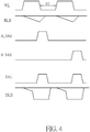
- FIG. 4 shows a timing diagram of some signals within the circuit 210 and the circuit 220 according to one embodiment of the present invention.
- the timing control circuit 130 generates a first control signal A_SAE and a second control signal B_SAE to the circuit 220, wherein the first control signal A_SAE is used to control the circuit 220 to generate the reading result ADO corresponding to the first read operation, and the second control signal B-SAE is used to control the circuit 220 to generate the reading result BDO corresponding to the second read operation.
- the timing control circuit 130 in a first half of a clock cycle, the timing control circuit 130 generates a multiplexer control signal to control the multiplexer 120 to output the address A_adr to the single-port memory 110, and the single-port memory 110 selects one memory cell corresponding to the address A_adr to generate output data at the bit lines BL and BLB. Then, the timing control circuit 130 generates the first control signal A_SAE having the enable state, and the OR gate 224 receives the first control signal A_SAE to generate the control signal SAE having the enable state to control the sense amplifier 222 to generate signals DL and DLB.
- the demultiplexer 226 is controlled by the first control signal A_SAE having the enable state to output data A_GBL (i.e., signals DL and DLB) into the latch 228, wherein the data stored in the latch 228 serves as the reading result ADO.
- the timing control circuit 130 generates the multiplexer control signal to control the multiplexer 120 to output the address B_adr to the single-port memory 110, and the single-port memory 110 selects one memory cell corresponding to the address B_adr to generate output data at the bit lines BL and BLB.
- the timing control circuit 130 generates the second control signal B_SAE having the enable state
- the OR gate 224 receives the second control signal B_SAE to generate the control signal SAE having the enable state to control the sense amplifier 222 to generate signals DL and DLB.
- the demultiplexer 226 is controlled by the second control signal B_SAE having the enable state to output data B_GBL (i.e., signals DL and DLB) into the latch 229, wherein the data stored in the latch 229 serves as the reading result BDO.
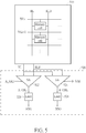
- FIG. 5 shows a circuit 510 within part of the single port memory 110 and a circuit 520 within part of the output circuit 140 according to another embodiment of the present invention. As shown in FIG.
- the single-port memory 110 comprises a memory cell array, each memory cell is used to store one bit.
- the circuit 510 shows some memory cells belonging to a complementary bit line pair including BL and BLB, and perpendicular to the bit lines are word lines such as WL i , WL i+1 .
- the circuit 520 within the output circuit 140 is coupled to one complementary bit line pair such as BL and BLB, and the circuit 520 is configured to get data from the bit lines BL/BLB to generate the two reading results ADO and BDO.
- the circuit 520 comprises two sense amplifiers 522 and 524, and two latches 526 and 528, wherein the each of the sense amplifiers 522 and 524 may have the structure shown in FIG. 3 .
- FIG. 6 shows a timing diagram of some signals within the circuit 510 and the circuit 520. Referring to FIGs. 1 , 5 and 6 together, regarding the operation of the circuit 510 and the circuit 520, in a first half of a clock cycle, the timing control circuit 130 generates a multiplexer control signal to control the multiplexer 120 to output the address A_adr to the single-port memory 110, and the single-port memory 110 selects one memory cell corresponding to the address A_adr to generate output data at the bit lines BL and BLB.
- the timing control circuit 130 generates the first control signal A_SAE having the enable state to control the sense amplifier 522 to generate data A_GBL (i.e., the signals DL and DLB, 'A_GLB' shown in FIG. 6 ) to the latch 526, wherein the data stored in the latch 526 serves as the reading result ADO; meanwhile, the second control signal B_SAE does not have the enable state, so that the sense amplifier 524 does not output any valid data when the sense amplifier 522 is enabled.
- A_GBL i.e., the signals DL and DLB, 'A_GLB' shown in FIG. 6
- the timing control circuit 130 generates the multiplexer control signal to control the multiplexer 120 to output the address B_adr to the single-port memory 110, and the single-port memory 110 selects one memory cell corresponding to the address B_adr to generate output data at the bit lines BL and BLB. Then, the timing control circuit 130 generates the second control signal B_SAE having the enable state to control the sense amplifier 524 to generate data B_GBL (i.e., the signals DL and DLB, 'B_GLB' shown in FIG.
- the first control signal A_SAE does not have the enable state, so that the sense amplifier 522 does not output any valid data when the sense amplifier 524 is enabled.
- the timing is dominated by the pre-charging of the bit lines BL/BLB, so the signal of B-port and the signal of A-port can partially overlap as shown in FIG. 6 . Therefore, the setup time (i.e. 'ST' shown in FIG. 4 ) from A-port to B-port is small, and the circuit 520 can operate in a faster speed to have better efficiency.
- the output circuit is only controlled by two control signals A_SAE and B_SAE to receive the output data from the single-port memory and output two reading results within a single clock cycle. Therefore, the present invention does not suffer the racing issue between many control signals.
- two sense amplifiers are designed to output two reading results separately in one clock cycle, to improve the efficiency of the pseudo dual-port memory.
Landscapes
- Engineering & Computer Science (AREA)
- Microelectronics & Electronic Packaging (AREA)
- Computer Hardware Design (AREA)
- Multimedia (AREA)
- Static Random-Access Memory (AREA)
- Dram (AREA)
- For Increasing The Reliability Of Semiconductor Memories (AREA)
Abstract
Description
- This application claims the priority of
US Provisional Application No. 63/010,715, filed on April 16th, 2020 - A dual-port memory handles two operations such as two read operations within a single clock cycle. A dual-port memory typically includes two ports operating with an array of memory cells, which may be simultaneously accessed from both ports. In order to reduce the area occupied by memory, a pseudo dual-port memory is used. The pseudo dual-port memory is designed to use a time-interleaving mechanism to perform two operations upon the single-port memory within a single clock cycle. For example, in a clock cycle, the pseudo dual-port memory may perform a first read operation, and then, perform a second read operation.
- Taking two read operations of the conventional pseudo dual-port as an example, a sense amplifier is enabled twice within a single clock signal to output two reading results, respectively, and the two reading results are temporarily stored in two latches, respectively. Each latch is controlled by a corresponding control signal to output the reading result in an appropriate time. However, the control signals of the sense amplifier and the two latches may suffer a racing issue.
- It is therefore an objective of the present invention to provide a pseudo dual-port memory, which is more robust and efficient, to solve the above-mentioned problems.
- According to one embodiment of the present invention, a pseudo dual-port memory is disclosed. The pseudo dual-port memory comprises a single-port memory, a multiplexer, a timing control circuit and an output circuit. The multiplexer is configured to receive a first address and a second address, and output one of the first address and the second address to the single-port memory. The timing control circuit is configured to generate a multiplexer control signal to control the multiplexer to sequentially output the first address and the second address to the single-port memory. The output circuit is configured to receive output data from the single-port memory to generate a first reading result corresponding to the first address and a second reading result corresponding to the second address. In addition, the output circuit comprises a sense amplifier and a demultiplexer. The sense amplifier is configured to receive the output data from the single-port memory to generate data according to a control signal, wherein the control signal is generated according to a first control signal and a second control signal generated by the timing control circuit. The demultiplexer is configured to output the data to a first latch when the first control signal has an enable state, and output the data to a second latch when the second control signal has the enable state, wherein the data stored in the first latch serves as the first reading result, and the data stored in the second latch serves as the second reading result.
- According to another embodiment of the present invention, a pseudo dual-port memory is disclosed. The pseudo dual-port memory comprises a single-port memory, a multiplexer, a timing control circuit and an output circuit. The multiplexer is configured to receive a first address and a second address, and output one of the first address and the second address to the single-port memory. The timing control circuit is configured to generate a multiplexer control signal to control the multiplexer to sequentially output the first address and the second address to the single-port memory. The output circuit is configured to receive output data from the single-port memory to generate a first reading result corresponding to the first address and a second reading result corresponding to the second address. In addition, the output circuit comprises a first sense amplifier and a second sense amplifier. The first sense amplifier is configured to receive the output data from the single-port memory to generate first data to a first latch according to a first control signal, wherein the first data stored in the first latch serves as the first reading result. The second sense amplifier is configured to receive the output data from the single-port memory to generate second data to a second latch according to a second control signal, wherein the second data stored in the second latch serves as the second reading result.
- According to another embodiment of the present invention, a control method of a pseudo dual-port memory is disclosed, wherein the pseudo dual-port memory comprises a single-port memory, a multiplexer and an output circuit: The multiplexer is configured to receive a first address and a second address, and output one of the first address and the second address to the single-port memory. The output circuit comprises a first sense amplifier and a second amplifier. The control method comprises the steps of: in a first half of a clock cycle of the pseudo dual-port memory: and controlling the multiplexer to input the first address to the single-port memory; enabling the first sense amplifier to receive output data of the single-port memory to generate first data serving as a first reading result corresponding to the first address; and in a second half of the clock cycle of the pseudo dual-port memory: controlling the multiplexer to input the second address to the single-port memory; and enabling the second sense amplifier to receive the output data of the single-port memory to generate second data serving as a second reading result corresponding to the first address.
- These and other objectives of the present invention will no doubt become obvious to those of ordinary skill in the art after reading the following detailed description of the preferred embodiment that is illustrated in the various figures and drawings.
-
-
FIG. 1 is a diagram illustrating a pseudo dual-port memory according to one embodiment of the present invention. -
FIG. 2 shows a circuit within part of the single port memory and a circuit within part of the output circuit according to one embodiment of the present invention. -
FIG. 3 shows the sense amplifier according to one embodiment of the present invention. -
FIG. 4 shows a timing diagram of some signals shown inFIG. 2 andFIG. 3 according to one embodiment of the present invention. -
FIG. 5 shows a circuit within part of the single port memory and a circuit within part of the output circuit according to another embodiment of the present invention. -
FIG. 6 shows a timing diagram of some signals shown inFIG. 5 andFIG. 3 according to one embodiment of the present invention. - Certain terms are used throughout the following description and claims to refer to particular system components. As one skilled in the art will appreciate, manufacturers may refer to a component by different names. This document does not intend to distinguish between components that differ in name but not function. In the following discussion and in the claims, the terms "including" and "comprising" are used in an open-ended fashion, and thus should be interpreted to mean "including, but not limited to ...". The terms "couple" and "couples" are intended to mean either an indirect or a direct electrical connection. Thus, if a first device couples to a second device, that connection may be through a direct electrical connection, or through an indirect electrical connection via other devices and connections.
-
FIG. 1 is a diagram illustrating a pseudo dual-port memory 100 according to one embodiment of the present invention. As shown inFIG. 1 , the pseudo dual-port memory 100 comprises a single-port memory 110, amultiplexer 120, atiming control circuit 130 and anoutput circuit 140. The pseudo dual-port memory 100 is designed to use a time-interleaving mechanism to perform two operations upon the single-port memory 110 within a single clock cycle. For example,FIG. 1 shows that two read operations are performed within one cycle (e.g., '1T') of a clock signal CK. In this embodiment, the pseudo dual-port memory 100 is a pseudo dual-port static random access memory (SRAM), that is the single-port memory 110 comprises a plurality of SRAM cells. - In the operation of the pseudo dual-
port memory 100, themultiplexer 120 may receive two addresses A_adr and B_adr, and in a first half of a clock cycle, thetiming control circuit 130 generates a multiplexer control signal to control themultiplexer 120 to output the address A_adr to the single-port memory 110, for the single-port memory 110 to select one memory cell corresponding to the address A_adr to generate an output data to theoutput circuit 140, then theoutput circuit 140 outputs a reading result ADO according to the output data. Then, in a second half of the clock cycle, thetiming control circuit 130 generates the multiplexer control signal to control themultiplexer 120 to output the address B_adr to the single-port memory 110, for the single-port memory 110 to select one memory cell corresponding to the address B_adr to generate an output data to theoutput circuit 140, then theoutput circuit 140 outputs a reading result BDO according to the output data. By using this time-interleaving mechanism, the pseudo dual-port memory 100 can perform two read operations within the single clock cycle to output two reading results ADO and BDO seq uentially. -
FIG. 2 shows acircuit 210 within part of thesingle port memory 110 and acircuit 220 within part of theoutput circuit 140 according to one embodiment of the present invention. As shown inFIG. 2 , the single-port memory 110 comprises a memory cell array, each memory cell is used to store one bit. Thecircuit 210 shows some memory cells belonging to a complementary bit line pair including BL and BLB, and perpendicular to the bit lines are word lines such as WL, WLi+1. Thecircuit 220 within theoutput circuit 140 is coupled to one complementary bit line pair such as BL and BLB, and thecircuit 220 is configured to get data from the bit lines BL/BLB to generate the two reading results ADO and BDO. - Specifically, the
circuit 220 comprises a sense amplifier (SA) 222, ademultiplexer 226, an OR gate and twolatches 228 and 229.FIG. 3 shows thesense amplifier 222 according to one embodiment of the present invention, wherein thesense amplifier 220 comprises transistors M1 - M11, wherein the transistor M1 is controlled by a control signal SAE, the transistors M4 and M11 are controlled by a signal DLEQ, the transistors M5 and M10 are controlled by a signal PBG that indicates a read operation when set to logic low, the transistors M6 and M9 are controlled by a pre-charge signal PRE. Thesense amplifier 220 is configured to receive signals from the bit lines BL and BLB to generate signals DL and DLB to the following circuit. Because the operation of thesense amplifier 220 is known by a person skilled in the art, the detailed descriptions about the transistors M1 - M11 are omitted here.FIG. 4 shows a timing diagram of some signals within thecircuit 210 and thecircuit 220 according to one embodiment of the present invention. Referring toFIGs. 1-4 together, regarding the operation of thecircuit 210 and thecircuit 220, thetiming control circuit 130 generates a first control signal A_SAE and a second control signal B_SAE to thecircuit 220, wherein the first control signal A_SAE is used to control thecircuit 220 to generate the reading result ADO corresponding to the first read operation, and the second control signal B-SAE is used to control thecircuit 220 to generate the reading result BDO corresponding to the second read operation. In detail, in a first half of a clock cycle, thetiming control circuit 130 generates a multiplexer control signal to control themultiplexer 120 to output the address A_adr to the single-port memory 110, and the single-port memory 110 selects one memory cell corresponding to the address A_adr to generate output data at the bit lines BL and BLB. Then, thetiming control circuit 130 generates the first control signal A_SAE having the enable state, and the OR gate 224 receives the first control signal A_SAE to generate the control signal SAE having the enable state to control thesense amplifier 222 to generate signals DL and DLB. At this time, thedemultiplexer 226 is controlled by the first control signal A_SAE having the enable state to output data A_GBL (i.e., signals DL and DLB) into thelatch 228, wherein the data stored in thelatch 228 serves as the reading result ADO. Then, in a second half of a clock cycle, thetiming control circuit 130 generates the multiplexer control signal to control themultiplexer 120 to output the address B_adr to the single-port memory 110, and the single-port memory 110 selects one memory cell corresponding to the address B_adr to generate output data at the bit lines BL and BLB. Then, thetiming control circuit 130 generates the second control signal B_SAE having the enable state, and the OR gate 224 receives the second control signal B_SAE to generate the control signal SAE having the enable state to control thesense amplifier 222 to generate signals DL and DLB. At this time, thedemultiplexer 226 is controlled by the second control signal B_SAE having the enable state to output data B_GBL (i.e., signals DL and DLB) into the latch 229, wherein the data stored in the latch 229 serves as the reading result BDO. - In light of above, because only the first control signal A_SAE and the second control signal B_SAE are used to control the
sense amplifier 222 and thedemultiplexer 226, this new design of thecircuit 220 does not have racing issue occurred in the previous design. - In the embodiment shown in
FIG. 2 , however, the timing is dominated by the pre-charging of the signal DL/DLB, so the efficiency may be influenced. Specifically, the B-port is triggered after the signal DLB is in pre-charging, so a larger setup time (i.e., 'ST' shown inFIG. 4 ) is required from A-port to B-port, where the A-port indicates the read operation corresponding to the first half of the clock cycle, and the B-port indicates the read operation corresponding to the second half of the clock cycle. To overcome this problem,FIG. 5 shows acircuit 510 within part of thesingle port memory 110 and acircuit 520 within part of theoutput circuit 140 according to another embodiment of the present invention. As shown inFIG. 5 , the single-port memory 110 comprises a memory cell array, each memory cell is used to store one bit. Thecircuit 510 shows some memory cells belonging to a complementary bit line pair including BL and BLB, and perpendicular to the bit lines are word lines such as WLi, WLi+1. Thecircuit 520 within theoutput circuit 140 is coupled to one complementary bit line pair such as BL and BLB, and thecircuit 520 is configured to get data from the bit lines BL/BLB to generate the two reading results ADO and BDO. - Specifically, the
circuit 520 comprises twosense amplifiers latches sense amplifiers FIG. 3 .FIG. 6 shows a timing diagram of some signals within thecircuit 510 and thecircuit 520. Referring toFIGs. 1 ,5 and6 together, regarding the operation of thecircuit 510 and thecircuit 520, in a first half of a clock cycle, thetiming control circuit 130 generates a multiplexer control signal to control themultiplexer 120 to output the address A_adr to the single-port memory 110, and the single-port memory 110 selects one memory cell corresponding to the address A_adr to generate output data at the bit lines BL and BLB. Then, thetiming control circuit 130 generates the first control signal A_SAE having the enable state to control thesense amplifier 522 to generate data A_GBL (i.e., the signals DL and DLB, 'A_GLB' shown inFIG. 6 ) to thelatch 526, wherein the data stored in thelatch 526 serves as the reading result ADO; meanwhile, the second control signal B_SAE does not have the enable state, so that thesense amplifier 524 does not output any valid data when thesense amplifier 522 is enabled. Then, in a second half of the clock cycle, thetiming control circuit 130 generates the multiplexer control signal to control themultiplexer 120 to output the address B_adr to the single-port memory 110, and the single-port memory 110 selects one memory cell corresponding to the address B_adr to generate output data at the bit lines BL and BLB. Then, thetiming control circuit 130 generates the second control signal B_SAE having the enable state to control thesense amplifier 524 to generate data B_GBL (i.e., the signals DL and DLB, 'B_GLB' shown inFIG. 6 ) to thelatch 528, wherein the data stored in thelatch 528 serves as the reading result BDO; meanwhile, the first control signal A_SAE does not have the enable state, so that thesense amplifier 522 does not output any valid data when thesense amplifier 524 is enabled. - In the embodiment shown in
FIG. 5 , the timing is dominated by the pre-charging of the bit lines BL/BLB, so the signal of B-port and the signal of A-port can partially overlap as shown inFIG. 6 . Therefore, the setup time (i.e. 'ST' shown inFIG. 4 ) from A-port to B-port is small, and thecircuit 520 can operate in a faster speed to have better efficiency. - Briefly summazied, in the pseudo dual-port memory of the present invention, the output circuit is only controlled by two control signals A_SAE and B_SAE to receive the output data from the single-port memory and output two reading results within a single clock cycle. Therefore, the present invention does not suffer the racing issue between many control signals. In one embodiment, two sense amplifiers are designed to output two reading results separately in one clock cycle, to improve the efficiency of the pseudo dual-port memory.
- Those skilled in the art will readily observe that numerous modifications and alterations of the device and method may be made while retaining the teachings of the invention. Accordingly, the above disclosure should be construed as limited only by the metes and bounds of the appended claims.
Claims (10)
- A pseudo dual-port memory (100), comprising:a single-port memory (110);a multiplexer (120), configured to receive a first address and a second address, and output one of the first address and the second address to the single-port memory (110);a timing control circuit (130), configured to generate a multiplexer (120) control signal to control the multiplexer (120) to sequentially output the first address and the second address to the single-port memory (110); andan output circuit (140), configured to receive output data from the single-port memory (110) to generate a first reading result corresponding to the first address and a second reading result corresponding to the second address; and the output circuit (140) comprises:a sense amplifier, configured to receive the output data from the single-port memory (110) to generate data according to a control signal, wherein the control signal is generated according to a first control signal and a second control signal generated by the timing control circuit (130); anda demultiplexer, coupled to the sense amplifier, configured to output the data to a first latch when the first control signal has an enable state, and output the data to a second latch when the second control signal has the enable state, wherein the data stored in the first latch serves as the first reading result, and the data stored in the second latch serves as the second reading result.
- The pseudo dual-port memory (100) of claim 1, wherein the timing control circuit (130) generates the multiplexer (120) control signal to control the multiplexer (120) to sequentially output the first address and the second address to the single-port memory (110) within a clock cycle, and the timing control circuit (1 30) further generates the first control signal and the second control signal to sequentially enable the sense amplifier to output the data of the first reading result and the second reading result.
- The pseudo dual-port memory (100) of claim 2, wherein the output circuit (140) further comprises an OR gate, and the OR gate receives the first control signal and the second control signal to generate the control signal to control the sense amplifier.
- The pseudo dual-port memory (100) of claim 2, wherein the control signal is generated by using the first control signal and the second control signal only.
- A pseudo dual-port memory (100), comprising:a single-port memory (110);a multiplexer (120), configured to receive a first address and a second address, and output one of the first address and the second address to the single-port memory (110);a timing control circuit (130), configured to generate a multiplexer (120) control signal to control the multiplexer (120) to sequentially output the first address and the second address to the single-port memory (110); andan output circuit (140), configured to receive output data from the single-port memory (110) to generate a first reading result corresponding to the first address and a second reading result corresponding to the second address; and the output circuit (140) comprises:a first sense amplifier, configured to receive the output data from the single-port memory (110) to generate first data to a first latch according to a first control signal, wherein the first data stored in the first latch serves as the first reading result; anda second sense amplifier, configured to receive the output data from the single-port memory (110) to generate second data to a second latch according to a second control signal, wherein the second data stored in the second latch serves as the second reading result.
- The pseudo dual-port memory (100) of claim 5, wherein the timing control circuit (130) generates the multiplexer (120) control signal to control the multiplexer (120) to sequentially output the first address and the second address to the single-port memory (110) within a clock cycle, and the timing control circuit (1 30) further generates the first control signal and the second control signal to sequentially enable the first sense amplifier and the second sense amplifier.
- The pseudo dual-port memory (100) of claim 6, wherein the first sense amplifier generates the first data to the first latch when the first control signal has an enable state, the second sense amplifier generates the second data to the second latch when the second control signal has the enable state, and the enable state of the firs control signal and the enable state of the second control signal is within the a single clock cycle.
- The pseudo dual-port memory (100) of claim 5, wherein a timing of a generation of the second data and a timing of a generation of the first data are partially overlapped.
- A control method of a pseudo dual-port memory (100), wherein the pseudo dual-port memory (100) comprises:a single-port memory (110);a multiplexer (120), configured to receive a first address and a second address, and output one of the first address and the second address to the single-port memory (110); andan output circuit (140) comprising a first sense amplifier and a second amplifier;wherein the control method comprises the steps of:in a first half of a clock cycle of the pseudo dual-port memory (100):controlling the multiplexer (120) to input the first address to the single-port memory (110);enabling the first sense amplifier to receive output data of the single-port memory (110) to generate first data serving as a first reading result corresponding to the first address; andin a second half of the clock cycle of the pseudo dual-port memory (100):controlling the multiplexer (120) to input the second address to the single-port memory (110);enabling the second sense amplifier to receive the output data of the single-port memory (110) to generate second data serving as a second reading result corresponding to the first address.
- The control method of claim 9, wherein a timing of a generation of the second data and a timing of a generation of the first data are partially overlapped.
Priority Applications (1)
| Application Number | Priority Date | Filing Date | Title |
|---|---|---|---|
| EP22184718.9A EP4095860A1 (en) | 2020-04-16 | 2021-03-30 | Time-interleaving sensing scheme for pseudo dual-port memory |
Applications Claiming Priority (2)
| Application Number | Priority Date | Filing Date | Title |
|---|---|---|---|
| US202063010715P | 2020-04-16 | 2020-04-16 | |
| US17/210,521 US11676657B2 (en) | 2020-04-16 | 2021-03-24 | Time-interleaving sensing scheme for pseudo dual-port memory |
Related Child Applications (2)
| Application Number | Title | Priority Date | Filing Date |
|---|---|---|---|
| EP22184718.9A Division EP4095860A1 (en) | 2020-04-16 | 2021-03-30 | Time-interleaving sensing scheme for pseudo dual-port memory |
| EP22184718.9A Division-Into EP4095860A1 (en) | 2020-04-16 | 2021-03-30 | Time-interleaving sensing scheme for pseudo dual-port memory |
Publications (3)
| Publication Number | Publication Date |
|---|---|
| EP3907737A2 true EP3907737A2 (en) | 2021-11-10 |
| EP3907737A3 EP3907737A3 (en) | 2021-12-22 |
| EP3907737B1 EP3907737B1 (en) | 2024-08-21 |
Family
ID=75339423
Family Applications (2)
| Application Number | Title | Priority Date | Filing Date |
|---|---|---|---|
| EP22184718.9A Withdrawn EP4095860A1 (en) | 2020-04-16 | 2021-03-30 | Time-interleaving sensing scheme for pseudo dual-port memory |
| EP21166023.8A Active EP3907737B1 (en) | 2020-04-16 | 2021-03-30 | Time-interleaving sensing scheme for pseudo dual-port memory |
Family Applications Before (1)
| Application Number | Title | Priority Date | Filing Date |
|---|---|---|---|
| EP22184718.9A Withdrawn EP4095860A1 (en) | 2020-04-16 | 2021-03-30 | Time-interleaving sensing scheme for pseudo dual-port memory |
Country Status (4)
| Country | Link |
|---|---|
| US (2) | US11676657B2 (en) |
| EP (2) | EP4095860A1 (en) |
| CN (1) | CN113611340B (en) |
| TW (1) | TWI758145B (en) |
Families Citing this family (4)
| Publication number | Priority date | Publication date | Assignee | Title |
|---|---|---|---|---|
| US11024347B2 (en) * | 2019-10-17 | 2021-06-01 | Marvell Asia Pte, Ltd. | Multiple sense amplifier and data path-based pseudo dual port SRAM |
| CN116136828A (en) * | 2021-11-17 | 2023-05-19 | 苏州盛科通信股份有限公司 | A multi-port storage device, reading and writing method, and device |
| US12518821B2 (en) * | 2022-09-23 | 2026-01-06 | Mediatek Inc. | Pseudo multi-port memory with memory cells each having two-port memory cell architecture and multiple enable pulses on same wordline and associated memory access method |
| KR102812286B1 (en) * | 2024-11-25 | 2025-05-23 | (주)라닉스 | Implementation Method for Synchronous 2-Port Memory Utilizing Single Port Architecture |
Family Cites Families (23)
| Publication number | Priority date | Publication date | Assignee | Title |
|---|---|---|---|---|
| US6272067B1 (en) * | 2000-07-11 | 2001-08-07 | Rosun Technologies, Inc. | SRAM synchronized with an optimized clock signal based on a delay and an external clock |
| KR100410988B1 (en) * | 2001-11-15 | 2003-12-18 | 삼성전자주식회사 | Semiconductor memory device and bit line sensing method thereof |
| JP2004022070A (en) * | 2002-06-17 | 2004-01-22 | Renesas Technology Corp | Semiconductor storage device |
| KR100604824B1 (en) * | 2003-08-08 | 2006-07-28 | 삼성전자주식회사 | Memory device and bitline sensing method employing bitline sense amplifier having arbitrary directionality by gate bias control |
| JP4673008B2 (en) | 2004-06-11 | 2011-04-20 | 株式会社リコー | Semiconductor memory device |
| US7251193B2 (en) | 2005-11-17 | 2007-07-31 | Qualcomm Incorporated | Pseudo-dual port memory where ratio of first to second memory access is clock duty cycle independent |
| US7319632B2 (en) * | 2005-11-17 | 2008-01-15 | Qualcomm Incorporated | Pseudo-dual port memory having a clock for each port |
| US20080155172A1 (en) * | 2006-12-22 | 2008-06-26 | Mediatek Inc. | Microcode patching system and method |
| US7529139B2 (en) | 2007-01-26 | 2009-05-05 | Mediatek, Inc. | N-port memory circuits allowing M memory addresses to be accessed concurrently and signal processing methods thereof |
| US7656731B2 (en) * | 2007-03-30 | 2010-02-02 | Qualcomm, Incorporated | Semi-shared sense amplifier and global read line architecture |
| JP2009123298A (en) | 2007-11-16 | 2009-06-04 | Renesas Technology Corp | Semiconductor integrated circuit device |
| US8379466B2 (en) * | 2009-03-31 | 2013-02-19 | Freescale Semiconductor, Inc. | Integrated circuit having an embedded memory and method for testing the memory |
| US8437215B2 (en) * | 2011-01-20 | 2013-05-07 | Taiwan Semiconductor Manufacturing Co., Ltd. | Memory with word-line segment access |
| US8514652B2 (en) | 2011-03-02 | 2013-08-20 | Lsi Corporation | Multiple-port memory device comprising single-port memory device with supporting control circuitry |
| US9047981B2 (en) * | 2012-12-21 | 2015-06-02 | Advanced Micro Devices, Inc. | Bit-flipping in memories |
| US8830766B2 (en) * | 2013-01-23 | 2014-09-09 | Lsi Corporation | Margin free PVT tolerant fast self-timed sense amplifier reset circuit |
| US10720205B2 (en) * | 2014-06-05 | 2020-07-21 | Gsi Technology, Inc. | Systems and methods involving multi-bank, dual-pipe memory circuitry |
| GB2530017B (en) * | 2014-08-26 | 2020-05-13 | Advanced Risc Mach Ltd | Double pumped memory techniques |
| US9520165B1 (en) * | 2015-06-19 | 2016-12-13 | Qualcomm Incorporated | High-speed pseudo-dual-port memory with separate precharge controls |
| US10049709B2 (en) * | 2015-12-31 | 2018-08-14 | Arm Limited | Port modes for use with memory |
| JP6637872B2 (en) | 2016-10-28 | 2020-01-29 | ルネサスエレクトロニクス株式会社 | Multiport memory and semiconductor device |
| US10032506B2 (en) * | 2016-12-12 | 2018-07-24 | Stmicroelectronics International N.V. | Configurable pseudo dual port architecture for use with single port SRAM |
| US10978139B2 (en) * | 2019-06-04 | 2021-04-13 | Qualcomm Incorporated | Dual-mode high-bandwidth SRAM with self-timed clock circuit |
-
2021
- 2021-03-24 US US17/210,521 patent/US11676657B2/en active Active
- 2021-03-25 CN CN202110320673.5A patent/CN113611340B/en active Active
- 2021-03-26 TW TW110110964A patent/TWI758145B/en active
- 2021-03-30 EP EP22184718.9A patent/EP4095860A1/en not_active Withdrawn
- 2021-03-30 EP EP21166023.8A patent/EP3907737B1/en active Active
-
2022
- 2022-08-24 US US17/894,191 patent/US11887660B2/en active Active
Also Published As
| Publication number | Publication date |
|---|---|
| CN113611340B (en) | 2025-04-25 |
| EP4095860A1 (en) | 2022-11-30 |
| US11676657B2 (en) | 2023-06-13 |
| US20220406373A1 (en) | 2022-12-22 |
| US11887660B2 (en) | 2024-01-30 |
| US20210327500A1 (en) | 2021-10-21 |
| TW202141495A (en) | 2021-11-01 |
| CN113611340A (en) | 2021-11-05 |
| EP3907737B1 (en) | 2024-08-21 |
| EP3907737A3 (en) | 2021-12-22 |
| TWI758145B (en) | 2022-03-11 |
Similar Documents
| Publication | Publication Date | Title |
|---|---|---|
| US11887660B2 (en) | Time-interleaving sensing scheme for pseudo dual-port memory | |
| US6359813B1 (en) | Semiconductor memory device having improved data transfer rate without providing a register for holding write data | |
| US8036056B2 (en) | Semiconductor memory device and method of inputting and outputting data in the semiconductor memory device | |
| JP2000163956A (en) | Semiconductor storage device | |
| US6795372B2 (en) | Bit line sense amplifier driving control circuits and methods for synchronous drams that selectively supply and suspend supply of operating voltages | |
| EP2082399B1 (en) | Memory bus output driver of a multi-bank memory device and method therefor | |
| KR100322534B1 (en) | Semiconductor device having DRAM &SRAM and Data transferring Method | |
| JPH11306758A (en) | Semiconductor storage device | |
| JP4477456B2 (en) | Semiconductor memory | |
| US6310818B1 (en) | Semiconductor memory device and method of changing output data of the same | |
| KR20010009561A (en) | method for preventing error of bypass operation and improving duration of cycle time in late-write type semiconductor memory device and multiplexer circuit therefor | |
| US7027347B2 (en) | Semiconductor memory device | |
| US6487132B2 (en) | Integrated circuit memory devices having multiple input/output buses and precharge circuitry for precharging the input/output buses between write operations | |
| KR100793671B1 (en) | Semiconductor Memory and Precharge Method | |
| US6044433A (en) | DRAM cache | |
| JP2001243764A (en) | Semiconductor storage device | |
| JP3079025B2 (en) | Serial access memory control circuit | |
| US6859400B2 (en) | Semiconductor memory device | |
| JPH10255459A (en) | Line memory | |
| US6434069B1 (en) | Two-phase charge-sharing data latch for memory circuit | |
| JPH10283781A (en) | Multi-port memory | |
| JP4673008B2 (en) | Semiconductor memory device | |
| US20050117422A1 (en) | Semiconductor integrated circuit including semiconductor memory | |
| JPH07244986A (en) | Semiconductor memory device | |
| JP3348520B2 (en) | Memory circuit |
Legal Events
| Date | Code | Title | Description |
|---|---|---|---|
| PUAI | Public reference made under article 153(3) epc to a published international application that has entered the european phase |
Free format text: ORIGINAL CODE: 0009012 |
|
| STAA | Information on the status of an ep patent application or granted ep patent |
Free format text: STATUS: THE APPLICATION HAS BEEN PUBLISHED |
|
| AK | Designated contracting states |
Kind code of ref document: A2 Designated state(s): AL AT BE BG CH CY CZ DE DK EE ES FI FR GB GR HR HU IE IS IT LI LT LU LV MC MK MT NL NO PL PT RO RS SE SI SK SM TR |
|
| PUAL | Search report despatched |
Free format text: ORIGINAL CODE: 0009013 |
|
| AK | Designated contracting states |
Kind code of ref document: A3 Designated state(s): AL AT BE BG CH CY CZ DE DK EE ES FI FR GB GR HR HU IE IS IT LI LT LU LV MC MK MT NL NO PL PT RO RS SE SI SK SM TR |
|
| RIC1 | Information provided on ipc code assigned before grant |
Ipc: G11C 7/08 20060101ALI20211116BHEP Ipc: G11C 8/06 20060101ALI20211116BHEP Ipc: G11C 7/22 20060101ALI20211116BHEP Ipc: G11C 7/10 20060101AFI20211116BHEP |
|
| STAA | Information on the status of an ep patent application or granted ep patent |
Free format text: STATUS: REQUEST FOR EXAMINATION WAS MADE |
|
| 17P | Request for examination filed |
Effective date: 20220613 |
|
| RBV | Designated contracting states (corrected) |
Designated state(s): AL AT BE BG CH CY CZ DE DK EE ES FI FR GB GR HR HU IE IS IT LI LT LU LV MC MK MT NL NO PL PT RO RS SE SI SK SM TR |
|
| STAA | Information on the status of an ep patent application or granted ep patent |
Free format text: STATUS: EXAMINATION IS IN PROGRESS |
|
| 17Q | First examination report despatched |
Effective date: 20221014 |
|
| P01 | Opt-out of the competence of the unified patent court (upc) registered |
Effective date: 20230607 |
|
| REG | Reference to a national code |
Ref country code: DE Free format text: PREVIOUS MAIN CLASS: G11C0007100000 Ref country code: DE Ref legal event code: R079 Ref document number: 602021017380 Country of ref document: DE Free format text: PREVIOUS MAIN CLASS: G11C0007100000 Ipc: G11C0007080000 |
|
| GRAP | Despatch of communication of intention to grant a patent |
Free format text: ORIGINAL CODE: EPIDOSNIGR1 |
|
| STAA | Information on the status of an ep patent application or granted ep patent |
Free format text: STATUS: GRANT OF PATENT IS INTENDED |
|
| RIC1 | Information provided on ipc code assigned before grant |
Ipc: G11C 11/419 20060101ALI20240312BHEP Ipc: G11C 7/06 20060101ALI20240312BHEP Ipc: G11C 7/08 20060101AFI20240312BHEP |
|
| INTG | Intention to grant announced |
Effective date: 20240325 |
|
| GRAS | Grant fee paid |
Free format text: ORIGINAL CODE: EPIDOSNIGR3 |
|
| GRAA | (expected) grant |
Free format text: ORIGINAL CODE: 0009210 |
|
| STAA | Information on the status of an ep patent application or granted ep patent |
Free format text: STATUS: THE PATENT HAS BEEN GRANTED |
|
| AK | Designated contracting states |
Kind code of ref document: B1 Designated state(s): AL AT BE BG CH CY CZ DE DK EE ES FI FR GB GR HR HU IE IS IT LI LT LU LV MC MK MT NL NO PL PT RO RS SE SI SK SM TR |
|
| REG | Reference to a national code |
Ref country code: GB Ref legal event code: FG4D |
|
| REG | Reference to a national code |
Ref country code: CH Ref legal event code: EP |
|
| REG | Reference to a national code |
Ref country code: DE Ref legal event code: R096 Ref document number: 602021017380 Country of ref document: DE |
|
| REG | Reference to a national code |
Ref country code: IE Ref legal event code: FG4D |
|
| REG | Reference to a national code |
Ref country code: LT Ref legal event code: MG9D |
|
| REG | Reference to a national code |
Ref country code: NL Ref legal event code: MP Effective date: 20240821 |
|
| PG25 | Lapsed in a contracting state [announced via postgrant information from national office to epo] |
Ref country code: NO Free format text: LAPSE BECAUSE OF FAILURE TO SUBMIT A TRANSLATION OF THE DESCRIPTION OR TO PAY THE FEE WITHIN THE PRESCRIBED TIME-LIMIT Effective date: 20241121 |
|
| REG | Reference to a national code |
Ref country code: AT Ref legal event code: MK05 Ref document number: 1716330 Country of ref document: AT Kind code of ref document: T Effective date: 20240821 |
|
| PG25 | Lapsed in a contracting state [announced via postgrant information from national office to epo] |
Ref country code: NL Free format text: LAPSE BECAUSE OF FAILURE TO SUBMIT A TRANSLATION OF THE DESCRIPTION OR TO PAY THE FEE WITHIN THE PRESCRIBED TIME-LIMIT Effective date: 20240821 Ref country code: PT Free format text: LAPSE BECAUSE OF FAILURE TO SUBMIT A TRANSLATION OF THE DESCRIPTION OR TO PAY THE FEE WITHIN THE PRESCRIBED TIME-LIMIT Effective date: 20241223 Ref country code: GR Free format text: LAPSE BECAUSE OF FAILURE TO SUBMIT A TRANSLATION OF THE DESCRIPTION OR TO PAY THE FEE WITHIN THE PRESCRIBED TIME-LIMIT Effective date: 20241122 Ref country code: PL Free format text: LAPSE BECAUSE OF FAILURE TO SUBMIT A TRANSLATION OF THE DESCRIPTION OR TO PAY THE FEE WITHIN THE PRESCRIBED TIME-LIMIT Effective date: 20240821 Ref country code: FI Free format text: LAPSE BECAUSE OF FAILURE TO SUBMIT A TRANSLATION OF THE DESCRIPTION OR TO PAY THE FEE WITHIN THE PRESCRIBED TIME-LIMIT Effective date: 20240821 |
|
| PG25 | Lapsed in a contracting state [announced via postgrant information from national office to epo] |
Ref country code: BG Free format text: LAPSE BECAUSE OF FAILURE TO SUBMIT A TRANSLATION OF THE DESCRIPTION OR TO PAY THE FEE WITHIN THE PRESCRIBED TIME-LIMIT Effective date: 20240821 |
|
| PG25 | Lapsed in a contracting state [announced via postgrant information from national office to epo] |
Ref country code: LV Free format text: LAPSE BECAUSE OF FAILURE TO SUBMIT A TRANSLATION OF THE DESCRIPTION OR TO PAY THE FEE WITHIN THE PRESCRIBED TIME-LIMIT Effective date: 20240821 |
|
| PG25 | Lapsed in a contracting state [announced via postgrant information from national office to epo] |
Ref country code: AT Free format text: LAPSE BECAUSE OF FAILURE TO SUBMIT A TRANSLATION OF THE DESCRIPTION OR TO PAY THE FEE WITHIN THE PRESCRIBED TIME-LIMIT Effective date: 20240821 Ref country code: IS Free format text: LAPSE BECAUSE OF FAILURE TO SUBMIT A TRANSLATION OF THE DESCRIPTION OR TO PAY THE FEE WITHIN THE PRESCRIBED TIME-LIMIT Effective date: 20241221 |
|
| PG25 | Lapsed in a contracting state [announced via postgrant information from national office to epo] |
Ref country code: HR Free format text: LAPSE BECAUSE OF FAILURE TO SUBMIT A TRANSLATION OF THE DESCRIPTION OR TO PAY THE FEE WITHIN THE PRESCRIBED TIME-LIMIT Effective date: 20240821 |
|
| PG25 | Lapsed in a contracting state [announced via postgrant information from national office to epo] |
Ref country code: RS Free format text: LAPSE BECAUSE OF FAILURE TO SUBMIT A TRANSLATION OF THE DESCRIPTION OR TO PAY THE FEE WITHIN THE PRESCRIBED TIME-LIMIT Effective date: 20241121 Ref country code: ES Free format text: LAPSE BECAUSE OF FAILURE TO SUBMIT A TRANSLATION OF THE DESCRIPTION OR TO PAY THE FEE WITHIN THE PRESCRIBED TIME-LIMIT Effective date: 20240821 |
|
| PG25 | Lapsed in a contracting state [announced via postgrant information from national office to epo] |
Ref country code: RS Free format text: LAPSE BECAUSE OF FAILURE TO SUBMIT A TRANSLATION OF THE DESCRIPTION OR TO PAY THE FEE WITHIN THE PRESCRIBED TIME-LIMIT Effective date: 20241121 Ref country code: PT Free format text: LAPSE BECAUSE OF FAILURE TO SUBMIT A TRANSLATION OF THE DESCRIPTION OR TO PAY THE FEE WITHIN THE PRESCRIBED TIME-LIMIT Effective date: 20241223 Ref country code: PL Free format text: LAPSE BECAUSE OF FAILURE TO SUBMIT A TRANSLATION OF THE DESCRIPTION OR TO PAY THE FEE WITHIN THE PRESCRIBED TIME-LIMIT Effective date: 20240821 Ref country code: NO Free format text: LAPSE BECAUSE OF FAILURE TO SUBMIT A TRANSLATION OF THE DESCRIPTION OR TO PAY THE FEE WITHIN THE PRESCRIBED TIME-LIMIT Effective date: 20241121 Ref country code: NL Free format text: LAPSE BECAUSE OF FAILURE TO SUBMIT A TRANSLATION OF THE DESCRIPTION OR TO PAY THE FEE WITHIN THE PRESCRIBED TIME-LIMIT Effective date: 20240821 Ref country code: LV Free format text: LAPSE BECAUSE OF FAILURE TO SUBMIT A TRANSLATION OF THE DESCRIPTION OR TO PAY THE FEE WITHIN THE PRESCRIBED TIME-LIMIT Effective date: 20240821 Ref country code: IS Free format text: LAPSE BECAUSE OF FAILURE TO SUBMIT A TRANSLATION OF THE DESCRIPTION OR TO PAY THE FEE WITHIN THE PRESCRIBED TIME-LIMIT Effective date: 20241221 Ref country code: HR Free format text: LAPSE BECAUSE OF FAILURE TO SUBMIT A TRANSLATION OF THE DESCRIPTION OR TO PAY THE FEE WITHIN THE PRESCRIBED TIME-LIMIT Effective date: 20240821 Ref country code: GR Free format text: LAPSE BECAUSE OF FAILURE TO SUBMIT A TRANSLATION OF THE DESCRIPTION OR TO PAY THE FEE WITHIN THE PRESCRIBED TIME-LIMIT Effective date: 20241122 Ref country code: FI Free format text: LAPSE BECAUSE OF FAILURE TO SUBMIT A TRANSLATION OF THE DESCRIPTION OR TO PAY THE FEE WITHIN THE PRESCRIBED TIME-LIMIT Effective date: 20240821 Ref country code: ES Free format text: LAPSE BECAUSE OF FAILURE TO SUBMIT A TRANSLATION OF THE DESCRIPTION OR TO PAY THE FEE WITHIN THE PRESCRIBED TIME-LIMIT Effective date: 20240821 Ref country code: BG Free format text: LAPSE BECAUSE OF FAILURE TO SUBMIT A TRANSLATION OF THE DESCRIPTION OR TO PAY THE FEE WITHIN THE PRESCRIBED TIME-LIMIT Effective date: 20240821 Ref country code: AT Free format text: LAPSE BECAUSE OF FAILURE TO SUBMIT A TRANSLATION OF THE DESCRIPTION OR TO PAY THE FEE WITHIN THE PRESCRIBED TIME-LIMIT Effective date: 20240821 |
|
| PG25 | Lapsed in a contracting state [announced via postgrant information from national office to epo] |
Ref country code: SM Free format text: LAPSE BECAUSE OF FAILURE TO SUBMIT A TRANSLATION OF THE DESCRIPTION OR TO PAY THE FEE WITHIN THE PRESCRIBED TIME-LIMIT Effective date: 20240821 Ref country code: RO Free format text: LAPSE BECAUSE OF FAILURE TO SUBMIT A TRANSLATION OF THE DESCRIPTION OR TO PAY THE FEE WITHIN THE PRESCRIBED TIME-LIMIT Effective date: 20240821 Ref country code: DK Free format text: LAPSE BECAUSE OF FAILURE TO SUBMIT A TRANSLATION OF THE DESCRIPTION OR TO PAY THE FEE WITHIN THE PRESCRIBED TIME-LIMIT Effective date: 20240821 |
|
| PG25 | Lapsed in a contracting state [announced via postgrant information from national office to epo] |
Ref country code: EE Free format text: LAPSE BECAUSE OF FAILURE TO SUBMIT A TRANSLATION OF THE DESCRIPTION OR TO PAY THE FEE WITHIN THE PRESCRIBED TIME-LIMIT Effective date: 20240821 |
|
| PG25 | Lapsed in a contracting state [announced via postgrant information from national office to epo] |
Ref country code: CZ Free format text: LAPSE BECAUSE OF FAILURE TO SUBMIT A TRANSLATION OF THE DESCRIPTION OR TO PAY THE FEE WITHIN THE PRESCRIBED TIME-LIMIT Effective date: 20240821 |
|
| PG25 | Lapsed in a contracting state [announced via postgrant information from national office to epo] |
Ref country code: IT Free format text: LAPSE BECAUSE OF FAILURE TO SUBMIT A TRANSLATION OF THE DESCRIPTION OR TO PAY THE FEE WITHIN THE PRESCRIBED TIME-LIMIT Effective date: 20240821 Ref country code: SK Free format text: LAPSE BECAUSE OF FAILURE TO SUBMIT A TRANSLATION OF THE DESCRIPTION OR TO PAY THE FEE WITHIN THE PRESCRIBED TIME-LIMIT Effective date: 20240821 |
|
| REG | Reference to a national code |
Ref country code: DE Ref legal event code: R097 Ref document number: 602021017380 Country of ref document: DE |
|
| PLBE | No opposition filed within time limit |
Free format text: ORIGINAL CODE: 0009261 |
|
| STAA | Information on the status of an ep patent application or granted ep patent |
Free format text: STATUS: NO OPPOSITION FILED WITHIN TIME LIMIT |
|
| 26N | No opposition filed |
Effective date: 20250522 |
|
| PG25 | Lapsed in a contracting state [announced via postgrant information from national office to epo] |
Ref country code: SE Free format text: LAPSE BECAUSE OF FAILURE TO SUBMIT A TRANSLATION OF THE DESCRIPTION OR TO PAY THE FEE WITHIN THE PRESCRIBED TIME-LIMIT Effective date: 20240821 |
|
| PG25 | Lapsed in a contracting state [announced via postgrant information from national office to epo] |
Ref country code: MC Free format text: LAPSE BECAUSE OF FAILURE TO SUBMIT A TRANSLATION OF THE DESCRIPTION OR TO PAY THE FEE WITHIN THE PRESCRIBED TIME-LIMIT Effective date: 20240821 |
|
| REG | Reference to a national code |
Ref country code: CH Ref legal event code: H13 Free format text: ST27 STATUS EVENT CODE: U-0-0-H10-H13 (AS PROVIDED BY THE NATIONAL OFFICE) Effective date: 20251023 |
|
| PG25 | Lapsed in a contracting state [announced via postgrant information from national office to epo] |
Ref country code: LU Free format text: LAPSE BECAUSE OF NON-PAYMENT OF DUE FEES Effective date: 20250330 |
|
| REG | Reference to a national code |
Ref country code: BE Ref legal event code: MM Effective date: 20250331 |
|
| PGFP | Annual fee paid to national office [announced via postgrant information from national office to epo] |
Ref country code: FR Payment date: 20251231 Year of fee payment: 6 |
|
| PG25 | Lapsed in a contracting state [announced via postgrant information from national office to epo] |
Ref country code: BE Free format text: LAPSE BECAUSE OF NON-PAYMENT OF DUE FEES Effective date: 20250331 |
|
| PG25 | Lapsed in a contracting state [announced via postgrant information from national office to epo] |
Ref country code: CH Free format text: LAPSE BECAUSE OF NON-PAYMENT OF DUE FEES Effective date: 20250331 |
|
| PG25 | Lapsed in a contracting state [announced via postgrant information from national office to epo] |
Ref country code: IE Free format text: LAPSE BECAUSE OF NON-PAYMENT OF DUE FEES Effective date: 20250330 |
|
| PGFP | Annual fee paid to national office [announced via postgrant information from national office to epo] |
Ref country code: GB Payment date: 20260106 Year of fee payment: 6 |
|
| PGFP | Annual fee paid to national office [announced via postgrant information from national office to epo] |
Ref country code: DE Payment date: 20260102 Year of fee payment: 6 |