EP3907613A1 - Reduzierter fehlerkorrekturcode für dynamischen doppelkanal-ddr-speicher mit direktzugriff - Google Patents
Reduzierter fehlerkorrekturcode für dynamischen doppelkanal-ddr-speicher mit direktzugriff Download PDFInfo
- Publication number
- EP3907613A1 EP3907613A1 EP21166791.0A EP21166791A EP3907613A1 EP 3907613 A1 EP3907613 A1 EP 3907613A1 EP 21166791 A EP21166791 A EP 21166791A EP 3907613 A1 EP3907613 A1 EP 3907613A1
- Authority
- EP
- European Patent Office
- Prior art keywords
- bytes
- data
- ecc
- channel
- ddr5
- Prior art date
- Legal status (The legal status is an assumption and is not a legal conclusion. Google has not performed a legal analysis and makes no representation as to the accuracy of the status listed.)
- Withdrawn
Links
Images


Classifications
-
- G—PHYSICS
- G11—INFORMATION STORAGE
- G11C—STATIC STORES
- G11C29/00—Checking stores for correct operation ; Subsequent repair; Testing stores during standby or offline operation
- G11C29/04—Detection or location of defective memory elements, e.g. cell constructio details, timing of test signals
- G11C29/08—Functional testing, e.g. testing during refresh, power-on self testing [POST] or distributed testing
- G11C29/12—Built-in arrangements for testing, e.g. built-in self testing [BIST] or interconnection details
- G11C29/38—Response verification devices
- G11C29/42—Response verification devices using error correcting codes [ECC] or parity check
-
- G—PHYSICS
- G06—COMPUTING OR CALCULATING; COUNTING
- G06F—ELECTRIC DIGITAL DATA PROCESSING
- G06F11/00—Error detection; Error correction; Monitoring
- G06F11/07—Responding to the occurrence of a fault, e.g. fault tolerance
- G06F11/08—Error detection or correction by redundancy in data representation, e.g. by using checking codes
- G06F11/10—Adding special bits or symbols to the coded information, e.g. parity check, casting out 9's or 11's
- G06F11/1008—Adding special bits or symbols to the coded information, e.g. parity check, casting out 9's or 11's in individual solid state devices
- G06F11/1044—Adding special bits or symbols to the coded information, e.g. parity check, casting out 9's or 11's in individual solid state devices with specific ECC/EDC distribution
-
- G—PHYSICS
- G06—COMPUTING OR CALCULATING; COUNTING
- G06F—ELECTRIC DIGITAL DATA PROCESSING
- G06F11/00—Error detection; Error correction; Monitoring
- G06F11/07—Responding to the occurrence of a fault, e.g. fault tolerance
- G06F11/08—Error detection or correction by redundancy in data representation, e.g. by using checking codes
- G06F11/10—Adding special bits or symbols to the coded information, e.g. parity check, casting out 9's or 11's
- G06F11/1008—Adding special bits or symbols to the coded information, e.g. parity check, casting out 9's or 11's in individual solid state devices
- G06F11/1048—Adding special bits or symbols to the coded information, e.g. parity check, casting out 9's or 11's in individual solid state devices using arrangements adapted for a specific error detection or correction feature
-
- G—PHYSICS
- G11—INFORMATION STORAGE
- G11C—STATIC STORES
- G11C29/00—Checking stores for correct operation ; Subsequent repair; Testing stores during standby or offline operation
- G11C29/04—Detection or location of defective memory elements, e.g. cell constructio details, timing of test signals
- G11C29/08—Functional testing, e.g. testing during refresh, power-on self testing [POST] or distributed testing
- G11C29/12—Built-in arrangements for testing, e.g. built-in self testing [BIST] or interconnection details
- G11C29/12015—Built-in arrangements for testing, e.g. built-in self testing [BIST] or interconnection details comprising clock generation or timing circuitry
-
- G—PHYSICS
- G11—INFORMATION STORAGE
- G11C—STATIC STORES
- G11C29/00—Checking stores for correct operation ; Subsequent repair; Testing stores during standby or offline operation
- G11C29/56—External testing equipment for static stores, e.g. automatic test equipment [ATE]; Interfaces therefor
- G11C29/56012—Timing aspects, clock generation, synchronisation
-
- G—PHYSICS
- G11—INFORMATION STORAGE
- G11C—STATIC STORES
- G11C29/00—Checking stores for correct operation ; Subsequent repair; Testing stores during standby or offline operation
- G11C29/70—Masking faults in memories by using spares or by reconfiguring
- G11C29/78—Masking faults in memories by using spares or by reconfiguring using programmable devices
- G11C29/80—Masking faults in memories by using spares or by reconfiguring using programmable devices with improved layout
- G11C29/816—Masking faults in memories by using spares or by reconfiguring using programmable devices with improved layout for an application-specific layout
- G11C29/824—Masking faults in memories by using spares or by reconfiguring using programmable devices with improved layout for an application-specific layout for synchronous memories
Definitions
- the present disclosure relates to improving memory channels and controllers.
- ECC error-correcting code
- a sender may encode a message with redundant information in the form of an ECC. The redundancy allows the receiver to detect a limited number of errors that may occur anywhere in the message, and often to correct these errors without retransmission.
- ECC covers any types of ECC, including block codes, convolutional codes, and the like. ECC may be used to protect the data stored in a memory device.
- a method comprising: receiving a first set of 64 bytes of data and a second set of 64 bytes of data; calculating a first set of eight error-correcting code (ECC) bytes for the first set of 64 bytes of data and a second set of eight ECC bytes for the second set of 64 bytes of data; and sending the first set of 64 bytes of data, the second set of 64 bytes of data, the first set of eight ECC bytes, and the second set of eight ECC bytes to one or more synchronous dynamic random-access memory (SDRAM) modules through a dual-channel in a single burst, wherein the dual-channel comprises a first data channel and a second data channel, and wherein the first data channel and the second data channel are driven by a same clock signal.
- ECC error-correcting code
- the one or more synchronous dynamic random-access memory (SDRAM) modules may comprise one or more 5th generation double data rate (DDR5) SDRAM, and wherein the dual-channel comprises a DDR5 dual-channel.
- DDR5 5th generation double data rate
- the DDR5 dual-channel may comprise a 72-bit wide DDR5 dual-channel.
- the 72-bit wide DDR5 dual-channel may comprise the first data channel with a 32-bit width, the second data channel with a 32-bit width, and an ECC channel with an 8-bit width.
- the first data channel and the second data channel of the DDR5 dual-channel may be driven by the same clock signal in lockstep.
- the sending of the first set of 64 bytes of data, the second set of 64 bytes of data, the first set of eight ECC bytes, and the second set of eight ECC bytes to the one or more 5th generation double data rate (DDR5) synchronous dynamic random-access memory (SDRAM) modules through the DDR5 dual-channel may have a burst length of 16 words.
- DDR5 5th generation double data rate
- SDRAM synchronous dynamic random-access memory
- the first set of eight ECC bytes may be used for error-correcting the entire first set of 64 bytes of data, and wherein the second set of eight ECC bytes is used to error correct the entire second set of 64 bytes of data.
- the sending of the first set of eight ECC bytes and the second set of eight ECC bytes may be in a predetermined order, and wherein the predetermined order is used to separate the ECC bytes for error-correcting the first set of 64 bytes of data and the ECC bytes for error-correcting the second set of 64 bytes of data that are read from the one or more 5th generation double data rate (DDR5) synchronous dynamic random-access memory (SDRAM) modules.
- DDR5 5th generation double data rate
- SDRAM synchronous dynamic random-access memory
- the sending of the first set of eight ECC bytes and the second set of eight ECC bytes may be in a predetermined order, and wherein the sending alternates between the two sets of eight ECC bytes.
- the sending of the first set of eight ECC bytes and the second set of eight ECC bytes may be in a predetermined order, and wherein the sending of the first set of eight ECC bytes is performed before the sending of the second set of eight ECC bytes.
- a system comprising: a first interface, the first interface configured to receive a first set of 64 bytes of data and a second set of 64 bytes of data; a processor, the processor configured to calculate a first set of eight error-correcting code (ECC) bytes for the first set of 64 bytes of data and a second set of eight ECC bytes for the second set of 64 bytes of data; and a second interface, the second interface configured to send the first set of 64 bytes of data, the second set of 64 bytes of data, the first set of eight ECC bytes, and the second set of eight ECC bytes to one or more synchronous dynamic random-access memory (SDRAM) modules through a dual-channel in a single burst, wherein the dual-channel comprises a first data channel and a second data channel, and wherein the first data channel and the second data channel are driven by a same clock signal.
- SDRAM synchronous dynamic random-access memory
- the one or more synchronous dynamic random-access memory (SDRAM) modules may comprise one or more 5th generation double data rate (DDR5) SDRAM, and wherein the dual-channel comprises a DDR5 dual-channel.
- DDR5 5th generation double data rate
- the DDR5 dual-channel may comprise a 72-bit wide DDR5 dual-channel.
- the 72-bit wide DDR5 dual-channel may comprise the first data channel with a 32-bit width, the second data channel with a 32-bit width, and an ECC channel with an 8-bit width.
- the first data channel and the second data channel of the DDR5 dual-channel may be driven by the same clock signal in lockstep.
- the sending of the first set of 64 bytes of data, the second set of 64 bytes of data, the first set of eight ECC bytes, and the second set of eight ECC bytes to the one or more 5th generation double data rate (DDR5) synchronous dynamic random-access memory (SDRAM) modules through the DDR5 dual-channel may have a burst length of 16 words.
- DDR5 5th generation double data rate
- SDRAM synchronous dynamic random-access memory
- the first set of eight ECC bytes may be used for error-correcting the entire first set of 64 bytes of data, and wherein the second set of eight ECC bytes is used to error correct the entire second set of 64 bytes of data.
- the sending of the first set of eight ECC bytes and the second set of eight ECC bytes may be in a predetermined order, and wherein the predetermined order is used to separate the ECC bytes for error-correcting the first set of 64 bytes of data and the ECC bytes for error-correcting the second set of 64 bytes of data that are read from the one or more 5th generation double data rate (DDR5) synchronous dynamic random-access memory (SDRAM) modules.
- DDR5 5th generation double data rate
- SDRAM synchronous dynamic random-access memory
- the sending of the first set of eight ECC bytes and the second set of eight ECC bytes may be in a predetermined order, and wherein the sending alternates between the two sets of eight ECC bytes.
- the sending of the first set of eight ECC bytes and the second set of eight ECC bytes may be in a predetermined order, and wherein the sending of the first set of eight ECC bytes is performed before the sending of the second set of eight ECC bytes.
- the invention can be implemented in numerous ways, including as a process; an apparatus; a system; a composition of matter; a computer program product embodied on a computer readable storage medium; and/or a processor, such as a processor configured to execute instructions stored on and/or provided by a memory coupled to the processor.
- these implementations, or any other form that the invention may take, may be referred to as techniques.
- the order of the steps of disclosed processes may be altered within the scope of the invention.
- a component such as a processor or a memory described as being configured to perform a task may be implemented as a general component that is temporarily configured to perform the task at a given time or a specific component that is manufactured to perform the task.
- the term 'processor' refers to one or more devices, circuits, and/or processing cores configured to process data, such as computer program instructions.
- Double Data Rate Synchronous Dynamic Random-Access Memory is a double data rate (DDR) synchronous dynamic random-access memory (SDRAM) class of memory integrated circuits used in computers.
- DDR SDRAM Double Data Rate Synchronous Dynamic Random-Access Memory
- DRAM dynamic random-access memory
- DRAM continues to increase in density and interface speeds continue to increase, the memory industry is transitioning from the 4 th generation DDR4 to the 5 th generation DDR5 industry standard.
- FIG. 1 illustrates a block diagram in which a memory controller 104 is used to access a group of DRAM modules 108.
- Memory controller 104 sends and receives data that flows between a processor and the processor's DRAM memory 108.
- the processor may be a central processing unit (CPU) or an accelerator.
- DRAM memory 108 may be any DDR SDRAM memory, such as a DDR4 or DDR5 SDRAM memory.
- memory controller 104 is integrated into another chip 102.
- the memory controller 104 may be placed on the same die or integrated as an integral part of a processor (e.g., a CPU or an accelerator).
- the memory controller 104 may be placed on the same die or integrated as part of an application-specific integrated circuit (ASIC), and the ASIC may be connected to a processor through an interconnect, such as Compute Express Link (CXL) or PCI Express (PCIe).
- CXL Compute Express Link
- PCIe PCI Express
- Memory controller 104 is a digital circuit that manages the flow of data going to and from the DRAM memory 108.
- Memory controller 104 contains the logic necessary for many different functions, including the logic to read and write to the DRAMs and also the logic to refresh the DRAMs. Memory controller 104 may also include the logic for error detection and correction.
- Memory controller 104 includes a memory physical interface (PHY) block 106.
- PHY block 106 includes the logic for connecting to the external DRAM memory 108.
- the DDR PHY Interface (DFI) is used as an interface protocol that defines the signals, timing, and programmable parameters required to transfer control information and data to and from the DRAM devices and between the memory controller 104 and the PHY block 106.
- DFI DDR PHY Interface
- DDR4 and DDR5 have different dual in-line memory module (DIMM) channel architectures.
- DIMM comprises a series of DRAM integrated circuits. These modules are mounted on a printed circuit board and designed for use in personal computers, workstations, and servers.
- Figure 2 illustrates an embodiment of a DDR4 channel.
- Figure 3 illustrates an embodiment of a traditional DDR5 channel.
- one of the changes as part of the transition from DDR4 to DDR5 is that the prefetch depth in the DRAMs, and therefore the burst length, has been increased from 8 to 16.
- DDR4 has a prefetch depth of 8n, and the basic burst size is eight words.
- Prefetch depth is the number of words of data that are fetched every time a column command is performed with DDR memories.
- Burst length is the amount of data transferred between the processor and its memory in each transmission. Because the core of the DRAM is much slower than the interface, the difference is bridged by accessing information in parallel and then serializing it out the interface.
- DDR4 prefetches eight words, which means that every time a read or a write operation is performed, it is performed on eight words of data, and bursts out of, or into, the SDRAM over four clock cycles on both clock edges, for a total of eight consecutive operations.
- DDR5 has a prefetch depth of 16n, and the basic burst size is 16 words.
- a burst length of 16 allows a single burst to access 64 bytes of data, which is the typical CPU cache line size. DDR5 achieves this by using only one of the two independent channels.
- the cache line size for different devices is 64 bytes.
- the bus width in DDR4 is 72 bits, with 64 data bits and eight error-correcting code (ECC) bits.
- ECC error-correcting code
- DDR4 DIMMs have a 72-bit bus, comprising 64 data bits and eight ECC bits.
- the bus width in DDR5 (see Figure 3 ) is changed to 40 bits, with 32 data bits and eight ECC bits.
- each DIMM has two 40-bit DDR5 channels, and each channel has 32 data bits and eight ECC bits.
- having two smaller independent channels improves memory access efficiency.
- each of the 40-bit DDR5 channels has its own independent clock, address, or control signals.
- the side-effect of this change is that for every 64 bytes of data, the amount of ECC data has increased from eight ECC bytes to 16 ECC bytes. In other words, the number of ECC bytes has doubled.
- the data to ECC ratio i.e., the amount of actual data over the amount of ECC data, is decreased from 8:1 to 4:1.
- the increased ECC overhead adds additional cost and power consumption to server systems.
- Figure 4 illustrates an embodiment in which DDR5 SDRAM memories are accessed using traditional DDR5 channels.
- Figure 5 illustrates an embodiment of a traditional DDR5 memory controller 404.
- two independent memory controllers (404 and 406) integrated into chip 402 are used to access two groups of DRAMs (408 and 410) independently.
- the DDR5 channel between memory controller 404 and its group of DRAMs and the DDR5 channel between memory controller 406 and its group of DRAMs are independent from each other.
- Each of the channels has its own independent clock, and the address and control signals for the channel are aligned to the channel's clock.
- each of the memory controllers includes, among other modules, a data engine 502, an ECC engine 504, and a PHY block 506.
- the ECC engine 504 computes 16 ECC bytes, corresponding to the 64 bytes of data.
- the 64 bytes of data and the 16 ECC bytes, a total of 80 bytes, are sent to the DRAMs by a single independent clock over a burst of 16 words.
- Figure 6 illustrates an embodiment in which DDR5 SDRAM memories are accessed using improved DDR5 channels.
- Figure 7 illustrates an embodiment of an improved DDR5 memory controller 605.
- a single improved memory controller 605 integrated into a chip 602 is used to access two groups of DRAMs (608 and 610).
- the two DDR5 channels between memory controller 605 and their corresponding groups of DRAMs are no longer independent from each other.
- the two DDR5 channels have timing dependency because each of the channels is driven by the same clock signal in lockstep, and the address and control signals for the channels are aligned to the same clock domain.
- the two groups of DRAMs (608 and 610) are no longer independent from each other. Reading and writing of the DRAMs are performed on the same clock, and the two groups of DRAMs need to be accessed in lockstep. Therefore, while the two groups of DRAMs may be physically separate groups of DRAMs, logically they belong to the same group of DRAMs.
- an improved memory controller 605 includes, among other modules, a data engine 702, an ECC engine 704, and a PHY block 706.
- An error-correcting code (ECC) is used for controlling errors in data over unreliable or noisy communication channels.
- a sender may encode a message with redundant information in the form of an ECC. The redundancy allows the receiver to detect a limited number of errors that may occur anywhere in the message, and often to correct these errors without retransmission.
- ECC covers any types of ECC, including block codes, convolutional codes, and the like.
- ECC engine 704 provides error correction to the data by generating the ECC bytes for the data and sending the ECC bytes to PHY block 706.
- the ECC engine 704 For each 128 bytes of data transferred from the processor to the data engine 702, the ECC engine 704 computes 16 ECC bytes corresponding to the 128 bytes of data.
- the 128 bytes of data and the 16 ECC bytes, a total of 144 bytes, are sent to the DRAMs by a single independent clock over a burst of 16 words.
- FIG. 8 illustrates an embodiment of a process 800 for sending data to one or more 5th generation double data rate (DDR5) synchronous dynamic random-access memory (SDRAM) modules by a memory controller.
- DDR5 5th generation double data rate
- SDRAM synchronous dynamic random-access memory
- a first set of 64 bytes of data and a second set of 64 bytes of data are received.
- a first set of eight error-correcting code (ECC) bytes for the first set of 64 bytes of data and a second set of eight ECC bytes for the second set of 64 bytes of data are calculated.
- ECC error-correcting code
- the first set of 64 bytes of data, the second set of 64 bytes of data, the first set of eight ECC bytes, and the second set of eight ECC bytes are sent to one or more 5 th generation double data rate (DDR5) synchronous dynamic random-access memory (SDRAM) modules through a DDR5 dual-channel in a single burst.
- DDR5 dual-channel comprises a first data channel and a second data channel, and wherein the first data channel and the second data channel are driven by a single clock signal.
- Figure 9 illustrates an embodiment of an improved DDR5 dual-channel.
- the prefetch depth is 16n, and the basic burst length is 16 words.
- the improved DDR5 dual-channel is a 72-bit dual-channel 902.
- memory controller 605 is configured to use a bus width of 72 bits, with 2x 32 data bits and 1x 8 ECC bits channel (see Figure 9 ).
- Each of the 32-bits data channels (904 and 906) transfers 64 bytes of data in one burst, which is protected by its own eight ECC bytes.
- the 2x 32-bits data channels (channel 904 and channel 906) are driven by the same clock signal in lockstep, transferring a block of 128 bytes of data at a time. To allow for independent commands, the address/control/command of channel 804 and channel 806 may be separated.
- the eight ECC bytes corresponding to each of the 32-bit data channels are used to error correct the entire 64 bytes of data in one burst, as long as the eight ECC bytes are sent within the burst, the eight ECC bytes may be used to error correct the data without causing any delay.
- the two data channels (904 and 906) are driven by the same clock signal in lockstep, as long as the 16 ECC bytes corresponding to the 128 bytes of data are sent within the burst, error correction for both of the data channels may be performed without any delay. Therefore, the 16 ECC bytes corresponding to the 128 bytes of data may be sent in any order.
- memory controller 605 may receive the combined 16 ECC bytes corresponding to channel 904 and channel 906 and organize the ECC bytes and send them out in a predetermined order.
- the 16 ECC bytes are interleaved.
- the eight ECC bytes corresponding to the left 32-bit data channel 904 (indicated by the shaded blocks) and the eight ECC bytes corresponding to the right 32-bit data channel 906 (indicated by the solid blocks) are interleaved together.
- the sending of the ECC bytes alternates between the two data channels.
- one ECC byte corresponding to the left 32-bit data channel 904 (indicated by a shaded block) is sent first, and one ECC byte corresponding to the right 32-bit data channel 906 (indicated by a solid block) is sent next, and a second ECC byte corresponding to the left 32-bit data channel 904 (indicated by a shaded block) is sent next, and then a second ECC byte corresponding to the right 32-bit data channel 906 (indicated by a solid block) is sent next, and so on.
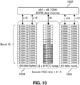
- Figure 10 illustrates another embodiment of an improved DDR5 dual-channel.
- the eight ECC bytes corresponding to the left 32-bit data channel 1004 (indicated by the shaded blocks) are sent first, and then the eight ECC bytes corresponding to the right 32-bit data channel 1006 (indicated by the solid blocks) are sent next.
- ECC bytes corresponding to the left 32-bit data channel are sent first, and then four ECC bytes corresponding to the right 32-bit data channel are sent next. Next, the remaining four ECC bytes corresponding to the left 32-bit data channel are sent, and then the remaining four ECC bytes corresponding to the right 32-bit data channel are sent.
- the ECC bytes are shown to be laid out in the middle of their respective 72-bit dual-channels (902 and 1002).
- memory controller 605 may map the data bytes and the ECC bytes across the address space in different ways.
- the ECC bytes may be stored across multiple DRAMs.
- Memory controller 605 keeps track of how the data bytes and the ECC bytes are being mapped across the 72-bit dual-channel. Accordingly, when memory controller 605 reads from the DRAMs, memory controller 605 may separate the data bytes and the ECC bytes according to the predetermined mapping. In addition, memory controller 605 keeps track of the order in which the ECC bytes corresponding to the two 32-bit data channels are being sent or received.
- memory controller 605 may separate the ECC bytes corresponding to the first data channel from those corresponding to the second data channel according to the predetermined ordering.
- the ECC bytes corresponding to each 32-bit data channel may then be used by memory controller 605 to detect or correct the errors of the data bytes belonging to that data channel.
- the benefit of the improved DDR5 dual-channel is that for every 64 bytes of data, the amount of ECC data is reduced from 16 ECC bytes (see Figure 3 ) to eight ECC bytes (see Figures 9 and 10 ). In other words, comparing to the DDR5 traditional technique, the number of ECC bytes for every 64 bytes of data is reduced by half.
- the data to ECC ratio i.e., the amount of actual data over the amount of ECC data, is increased from 4:1 to 8:1, which is the same as that for DDR4.
- the decreased ECC overhead reduces the cost and power consumption of server systems, which is beneficial when the extra ECC protection is not needed.
- the amount of ECC data is 16 bytes. In other words, keeping the same number of 16 ECC bytes, the improved DDR5 dual-channel transfers twice the amount of data.
Landscapes
- Engineering & Computer Science (AREA)
- Theoretical Computer Science (AREA)
- Quality & Reliability (AREA)
- Physics & Mathematics (AREA)
- General Engineering & Computer Science (AREA)
- General Physics & Mathematics (AREA)
- Dram (AREA)
- Techniques For Improving Reliability Of Storages (AREA)
Applications Claiming Priority (2)
| Application Number | Priority Date | Filing Date | Title |
|---|---|---|---|
| US202063019697P | 2020-05-04 | 2020-05-04 | |
| US16/938,865 US11437114B1 (en) | 2020-05-04 | 2020-07-24 | Reduced error correction code for dual channel DDR dynamic random-access memory |
Publications (1)
| Publication Number | Publication Date |
|---|---|
| EP3907613A1 true EP3907613A1 (de) | 2021-11-10 |
Family
ID=75362543
Family Applications (1)
| Application Number | Title | Priority Date | Filing Date |
|---|---|---|---|
| EP21166791.0A Withdrawn EP3907613A1 (de) | 2020-05-04 | 2021-04-01 | Reduzierter fehlerkorrekturcode für dynamischen doppelkanal-ddr-speicher mit direktzugriff |
Country Status (3)
| Country | Link |
|---|---|
| US (1) | US11437114B1 (de) |
| EP (1) | EP3907613A1 (de) |
| CN (1) | CN113611351A (de) |
Families Citing this family (3)
| Publication number | Priority date | Publication date | Assignee | Title |
|---|---|---|---|---|
| CN114400030A (zh) * | 2021-12-09 | 2022-04-26 | 芯河半导体科技(无锡)有限公司 | Ddr4接口数据交错走线的识别与重映射方法 |
| US12112049B2 (en) * | 2022-10-31 | 2024-10-08 | ScaleFlux, Inc. | Reducing energy consumption of self-managed DRAM modules |
| US20240243112A1 (en) * | 2023-01-12 | 2024-07-18 | Meta Platforms, Inc. | Three Dimensional Application-Specific Integrated Circuit Architecture |
Citations (3)
| Publication number | Priority date | Publication date | Assignee | Title |
|---|---|---|---|---|
| US7519894B2 (en) * | 2005-06-14 | 2009-04-14 | Infineon Technologies Ag | Memory device with error correction code module |
| US20090327596A1 (en) * | 2008-06-27 | 2009-12-31 | Intel Corporation | Memory controller using time-staggered lockstep sub-channels with buffered memory |
| US20200075079A1 (en) * | 2018-01-03 | 2020-03-05 | International Business Machines Corporation | Using dual channel memory as single channel memory with spares |
Family Cites Families (10)
| Publication number | Priority date | Publication date | Assignee | Title |
|---|---|---|---|---|
| US9703625B1 (en) * | 2013-03-14 | 2017-07-11 | Cadence Design Systems, Inc. | Method and apparatus for detecting or correcting multi-bit errors in computer memory systems |
| KR102189757B1 (ko) * | 2014-07-30 | 2020-12-11 | 삼성전자주식회사 | 반도체 메모리 장치, 이를 포함하는 메모리 시스템, 및 이의 동작 방법 |
| US10146711B2 (en) * | 2016-01-11 | 2018-12-04 | Intel Corporation | Techniques to access or operate a dual in-line memory module via multiple data channels |
| EP3453022B1 (de) * | 2016-05-02 | 2022-07-06 | INTEL Corporation | Interne fehlerüberprüfung und -korrektur (ecc) mit zusätzlichen systembits |
| US10268541B2 (en) * | 2016-08-15 | 2019-04-23 | Samsung Electronics Co., Ltd. | DRAM assist error correction mechanism for DDR SDRAM interface |
| US10628343B2 (en) * | 2017-02-03 | 2020-04-21 | Futurewei Technologies, Inc. | Systems and methods for utilizing DDR4-DRAM chips in hybrid DDR5-DIMMs and for cascading DDR5-DIMMs |
| US10606692B2 (en) * | 2017-12-20 | 2020-03-31 | International Business Machines Corporation | Error correction potency improvement via added burst beats in a dram access cycle |
| US10671497B2 (en) * | 2018-01-19 | 2020-06-02 | International Business Machines Corporation | Efficient and selective sparing of bits in memory systems |
| KR102718466B1 (ko) * | 2018-08-07 | 2024-10-17 | 삼성전자주식회사 | 메모리 컨트롤러, 메모리 컨트롤러의 동작 방법 및 메모리 시스템 |
| KR102770731B1 (ko) * | 2018-10-24 | 2025-02-24 | 삼성전자주식회사 | 메모리 모듈 및 메모리 시스템의 동작 방법 |
-
2020
- 2020-07-24 US US16/938,865 patent/US11437114B1/en active Active
-
2021
- 2021-04-01 EP EP21166791.0A patent/EP3907613A1/de not_active Withdrawn
- 2021-05-06 CN CN202110491746.7A patent/CN113611351A/zh active Pending
Patent Citations (3)
| Publication number | Priority date | Publication date | Assignee | Title |
|---|---|---|---|---|
| US7519894B2 (en) * | 2005-06-14 | 2009-04-14 | Infineon Technologies Ag | Memory device with error correction code module |
| US20090327596A1 (en) * | 2008-06-27 | 2009-12-31 | Intel Corporation | Memory controller using time-staggered lockstep sub-channels with buffered memory |
| US20200075079A1 (en) * | 2018-01-03 | 2020-03-05 | International Business Machines Corporation | Using dual channel memory as single channel memory with spares |
Non-Patent Citations (2)
| Title |
|---|
| ANAND LAL SHIMPI: "The Chipset - Intel's E7500 Chipset: Dual Channel DDR for Xeon", 25 February 2002 (2002-02-25), pages 1 - 4, XP055970080, Retrieved from the Internet <URL:https://www.anandtech.com/show/880/3> [retrieved on 20221011] * |
| SCHLACHTER SCOTT ET AL: "A MICRON WHITE PAPER Introducing Micron DDR5 SDRAM: More Than a Generational Update", 31 May 2019 (2019-05-31), pages 1 - 6, XP055844818, Retrieved from the Internet <URL:https://www.micron.com/-/media/client/global/documents/products/white-paper/ddr5_more_than_a_generational_update_wp.pdf?la=en> [retrieved on 20210927] * |
Also Published As
| Publication number | Publication date |
|---|---|
| US11437114B1 (en) | 2022-09-06 |
| CN113611351A (zh) | 2021-11-05 |
Similar Documents
| Publication | Publication Date | Title |
|---|---|---|
| US7836378B2 (en) | System to detect and identify errors in control information, read data and/or write data | |
| CN110377453B (zh) | 半导体存储器装置和包括半导体存储器装置的存储器系统 | |
| US6839266B1 (en) | Memory module with offset data lines and bit line swizzle configuration | |
| US8392796B2 (en) | Reliability, availability, and serviceability solution for memory technology | |
| US8255783B2 (en) | Apparatus, system and method for providing error protection for data-masking bits | |
| US7584336B2 (en) | Systems and methods for providing data modification operations in memory subsystems | |
| US7484161B2 (en) | System, method and storage medium for providing fault detection and correction in a memory subsystem | |
| US8359521B2 (en) | Providing a memory device having a shared error feedback pin | |
| US8023358B2 (en) | System and method for providing a non-power-of-two burst length in a memory system | |
| US20080155136A1 (en) | Memory controller, computer, and data read method | |
| US20130010552A1 (en) | Multi-mode memory device and method having stacked memory dice, a logic die and a command processing circuit and operating in direct and indirect modes | |
| US20100005375A1 (en) | Cyclical redundancy code for use in a high-speed serial link | |
| US8046663B2 (en) | Semiconductor memory device and method for driving the same | |
| EP3907613A1 (de) | Reduzierter fehlerkorrekturcode für dynamischen doppelkanal-ddr-speicher mit direktzugriff | |
| US7697332B2 (en) | Placement and routing of ECC memory devices for improved signal timing | |
| US20040237001A1 (en) | Memory integrated circuit including an error detection mechanism for detecting errors in address and control signals | |
| EP3268864A2 (de) | Hochleistungsfähiges nichtflüchtiges speichermodul | |
| KR20240062654A (ko) | 반도체 메모리 장치 및 반도체 메모리 장치의 동작 방법 | |
| US20170344275A1 (en) | Memory system with threaded transaction support | |
| US20150106678A1 (en) | Semiconductor device and semiconductor system including the same | |
| KR102427323B1 (ko) | 반도체 메모리 모듈, 반도체 메모리 시스템, 그리고 반도체 메모리 모듈을 액세스하는 액세스 방법 | |
| US20260127070A1 (en) | Buffer Component for Interleaving Data and Metadata for Error Correction | |
| CN117437966A (zh) | 半导体存储器装置和包括半导体存储器装置的存储器系统 | |
| CN120994130A (zh) | 数据传输方法、内存控制器、芯片及电子设备 |
Legal Events
| Date | Code | Title | Description |
|---|---|---|---|
| PUAI | Public reference made under article 153(3) epc to a published international application that has entered the european phase |
Free format text: ORIGINAL CODE: 0009012 |
|
| STAA | Information on the status of an ep patent application or granted ep patent |
Free format text: STATUS: THE APPLICATION HAS BEEN PUBLISHED |
|
| AK | Designated contracting states |
Kind code of ref document: A1 Designated state(s): AL AT BE BG CH CY CZ DE DK EE ES FI FR GB GR HR HU IE IS IT LI LT LU LV MC MK MT NL NO PL PT RO RS SE SI SK SM TR |
|
| B565 | Issuance of search results under rule 164(2) epc |
Effective date: 20211007 |
|
| STAA | Information on the status of an ep patent application or granted ep patent |
Free format text: STATUS: REQUEST FOR EXAMINATION WAS MADE |
|
| 17P | Request for examination filed |
Effective date: 20220506 |
|
| RBV | Designated contracting states (corrected) |
Designated state(s): AL AT BE BG CH CY CZ DE DK EE ES FI FR GB GR HR HU IE IS IT LI LT LU LV MC MK MT NL NO PL PT RO RS SE SI SK SM TR |
|
| RAP3 | Party data changed (applicant data changed or rights of an application transferred) |
Owner name: META PLATFORMS, INC. |
|
| STAA | Information on the status of an ep patent application or granted ep patent |
Free format text: STATUS: EXAMINATION IS IN PROGRESS |
|
| 17Q | First examination report despatched |
Effective date: 20221018 |
|
| STAA | Information on the status of an ep patent application or granted ep patent |
Free format text: STATUS: THE APPLICATION IS DEEMED TO BE WITHDRAWN |
|
| 18D | Application deemed to be withdrawn |
Effective date: 20240516 |