EP3905604A1 - Semiconductor device and method for protecting bus - Google Patents
Semiconductor device and method for protecting bus Download PDFInfo
- Publication number
- EP3905604A1 EP3905604A1 EP21169394.0A EP21169394A EP3905604A1 EP 3905604 A1 EP3905604 A1 EP 3905604A1 EP 21169394 A EP21169394 A EP 21169394A EP 3905604 A1 EP3905604 A1 EP 3905604A1
- Authority
- EP
- European Patent Office
- Prior art keywords
- data
- protocol
- bus
- verification
- master
- Prior art date
- Legal status (The legal status is an assumption and is not a legal conclusion. Google has not performed a legal analysis and makes no representation as to the accuracy of the status listed.)
- Granted
Links
Images


Classifications
-
- G—PHYSICS
- G06—COMPUTING OR CALCULATING; COUNTING
- G06F—ELECTRIC DIGITAL DATA PROCESSING
- G06F13/00—Interconnection of, or transfer of information or other signals between, memories, input/output devices or central processing units
- G06F13/14—Handling requests for interconnection or transfer
- G06F13/36—Handling requests for interconnection or transfer for access to common bus or bus system
- G06F13/362—Handling requests for interconnection or transfer for access to common bus or bus system with centralised access control
-
- H—ELECTRICITY
- H04—ELECTRIC COMMUNICATION TECHNIQUE
- H04L—TRANSMISSION OF DIGITAL INFORMATION, e.g. TELEGRAPHIC COMMUNICATION
- H04L12/00—Data switching networks
- H04L12/28—Data switching networks characterised by path configuration, e.g. LAN [Local Area Networks] or WAN [Wide Area Networks]
- H04L12/40—Bus networks
-
- G—PHYSICS
- G06—COMPUTING OR CALCULATING; COUNTING
- G06F—ELECTRIC DIGITAL DATA PROCESSING
- G06F11/00—Error detection; Error correction; Monitoring
- G06F11/07—Responding to the occurrence of a fault, e.g. fault tolerance
- G06F11/14—Error detection or correction of the data by redundancy in operations
- G06F11/1402—Saving, restoring, recovering or retrying
- G06F11/1405—Saving, restoring, recovering or retrying at machine instruction level
- G06F11/141—Saving, restoring, recovering or retrying at machine instruction level for bus or memory accesses
-
- G—PHYSICS
- G06—COMPUTING OR CALCULATING; COUNTING
- G06F—ELECTRIC DIGITAL DATA PROCESSING
- G06F11/00—Error detection; Error correction; Monitoring
- G06F11/07—Responding to the occurrence of a fault, e.g. fault tolerance
- G06F11/0703—Error or fault processing not based on redundancy, i.e. by taking additional measures to deal with the error or fault not making use of redundancy in operation, in hardware, or in data representation
- G06F11/0766—Error or fault reporting or storing
- G06F11/0772—Means for error signaling, e.g. using interrupts, exception flags, dedicated error registers
-
- G—PHYSICS
- G06—COMPUTING OR CALCULATING; COUNTING
- G06F—ELECTRIC DIGITAL DATA PROCESSING
- G06F11/00—Error detection; Error correction; Monitoring
- G06F11/07—Responding to the occurrence of a fault, e.g. fault tolerance
- G06F11/08—Error detection or correction by redundancy in data representation, e.g. by using checking codes
- G06F11/10—Adding special bits or symbols to the coded information, e.g. parity check, casting out 9's or 11's
- G06F11/1004—Adding special bits or symbols to the coded information, e.g. parity check, casting out 9's or 11's to protect a block of data words, e.g. CRC or checksum
-
- G—PHYSICS
- G06—COMPUTING OR CALCULATING; COUNTING
- G06F—ELECTRIC DIGITAL DATA PROCESSING
- G06F13/00—Interconnection of, or transfer of information or other signals between, memories, input/output devices or central processing units
- G06F13/14—Handling requests for interconnection or transfer
- G06F13/16—Handling requests for interconnection or transfer for access to memory bus
- G06F13/1668—Details of memory controller
-
- G—PHYSICS
- G06—COMPUTING OR CALCULATING; COUNTING
- G06F—ELECTRIC DIGITAL DATA PROCESSING
- G06F13/00—Interconnection of, or transfer of information or other signals between, memories, input/output devices or central processing units
- G06F13/38—Information transfer, e.g. on bus
- G06F13/382—Information transfer, e.g. on bus using universal interface adapter
- G06F13/387—Information transfer, e.g. on bus using universal interface adapter for adaptation of different data processing systems to different peripheral devices, e.g. protocol converters for incompatible systems, open system
-
- H—ELECTRICITY
- H04—ELECTRIC COMMUNICATION TECHNIQUE
- H04L—TRANSMISSION OF DIGITAL INFORMATION, e.g. TELEGRAPHIC COMMUNICATION
- H04L1/00—Arrangements for detecting or preventing errors in the information received
- H04L1/004—Arrangements for detecting or preventing errors in the information received by using forward error control
- H04L1/0056—Systems characterized by the type of code used
- H04L1/0061—Error detection codes
-
- G—PHYSICS
- G06—COMPUTING OR CALCULATING; COUNTING
- G06F—ELECTRIC DIGITAL DATA PROCESSING
- G06F11/00—Error detection; Error correction; Monitoring
- G06F11/07—Responding to the occurrence of a fault, e.g. fault tolerance
- G06F11/16—Error detection or correction of the data by redundancy in hardware
- G06F11/20—Error detection or correction of the data by redundancy in hardware using active fault-masking, e.g. by switching out faulty elements or by switching in spare elements
- G06F11/2002—Error detection or correction of the data by redundancy in hardware using active fault-masking, e.g. by switching out faulty elements or by switching in spare elements where interconnections or communication control functionality are redundant
- G06F11/2005—Error detection or correction of the data by redundancy in hardware using active fault-masking, e.g. by switching out faulty elements or by switching in spare elements where interconnections or communication control functionality are redundant using redundant communication controllers
Definitions
- the present invention relates to methods of protecting semiconductor device and buses.
- Patent Document 1 Japanese Unexamined Patent Application Publication No. 2010-211347
- Patent Document 1 discloses information processing device using error-detection codes (EDC: Error Detecting Code).
- the information processing device of Patent Document 1 includes an error detection code generation unit and an error detection unit.
- the error detection code generation unit generates EDC based on the address data from the bus master.
- the error detection unit generates EDC based on the address data corresponding to the bus slave, and compares it with EDC from the error detection code generation unit.
- Bus may use multiple protocols, not just a single protocol, such as Patent Document 1.
- protocol conversion is performed as appropriate in the bus.
- the data to be protected by EDC may change each time that a protocol conversion is performed. As a result, it was feared that it would be difficult to protect buses.
- Semiconductor device of an embodiment includes a bus master and a bus slave, a master interface provided between the bus master and the bus, a slave interface provided between the bus slave and the bus, and a protocol conversion unit provided in the bus.
- the bus master outputs the first data generated based on the first protocol.
- the master interface includes a copy data generation unit for generating copy data by copying the first data, and a code generation unit for generating an error detection code based on the copy data.
- the protocol conversion unit generates the second data by converting the first data from the first protocol to the second protocol.
- the slave interface is inputted with a second data, copy data, and error detection code, and includes an error detection unit, a protocol conversion unit for verification, and a comparator.
- the error detection unit detects the error of the copy data based on the error detection code.
- the protocol conversion unit for verification generates the first verification data by converting from one of the first protocol or the second protocol to the other for one of the second data or copy data.
- the comparator compares the second verification data with the first verification data, using the other of the second data or copied data as the second verification data.
- Using semiconductor device of one embodiment enables the bus to be protected even if the bus is protocol-converted.
- the description when required for convenience, the description will be made by dividing into a plurality of sections or embodiments, but except when specifically stated, they are not independent of each other, and one is related to the modified example, detail, supplementary description, or the like of part or all of the other.
- the number of elements, etc. (including the number of elements, numerical values, quantities, ranges, etc.) is not limited to the specific number, but may be not less than or equal to the specific number, except for cases where the number is specifically indicated and is clearly limited to the specific number in principle.
- the constituent elements are not necessarily essential except in the case where they are specifically specified and the case where they are considered to be obviously essential in principle.
- the shapes and the like are substantially approximate to or similar to the shapes and the like, except for the case in which they are specifically specified and the case in which they are considered to be obvious in principle, and the like. The same applies to the above numerical values and ranges.
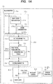
- FIG. 1A is a block diagram showing a configuration example of a main part in semiconductor device according to first embodiment of the present invention.
- FIG. 1B is a block diagram showing a configuration example of a main portion of the slave interface in the FIG. 1A .
- FIG. 2 is a schematic diagram showing a configuration example of the request data in FIG. 1 .
- Semiconductor device 1A in FIG. 1A is composed of one semiconductor chip, for example, a microcontroller, a SoC (System on Chip) or the like.
- Semiconductor device 1A of FIG. 1A includes a bus master 10a, a master interface 20A, a bus 30A, a slave interface 40A, a bus slave 15, and an error control unit 50.
- the bus master 10a performs various requests to the bus slave 15 via the bus 30A.
- the bus slave 15 performs various responses to the bus master 10a via the bus 30A.
- the master interface 20A is provided between the bus master 10a and the bus 30A corresponding to the bus master 10a and is an interface between the bus master 10a and the bus 30A.
- the slave interface 40A is provided between the bus slave 15 and the bus 30A corresponding to the bus slave 15 and is an interface between the bus slave 15 and the bus 30A.
- the bus 30A includes a protocol conversion unit 32a, and connects between the master interface 20A and the slave interface 40A.
- the bus master 10a outputs the request data (first data) RQa generated based on the protocol A.
- request data RQ includes, for example, information of the address, information of the burst type, information of the burst data size, information of the burst length, etc.
- the request data RQ may be constructed on a variety of formats depending on the protocol being used, not limited thereto.
- the master interface 20A includes a copy data generation unit 21a and a code generation unit 22a.
- the copy data generation unit 21a generates a copy data CRQa by copying the request data RQa.
- the code generation unit 22a generates an error detection code EDCa based on the copy-data CRQa. Then the master interface 20A outputs the request data RQa, the copy data CRQa, and the error detection code EDCa to the bus 30A.
- the protocol conversion unit 32a generates the request data RQb (second data) by converting the request data RQa from the master interface 20A from protocol A to the protocol B.
- the protocol conversion unit 32a for example, the correspondence between the data format based on the protocol A and the data format based on the protocol B is defined in the protocol conversion table 34a in advance.
- Protocol conversion table 34a for example, is configured by using a logic circuit, or is configured by combining a storage circuit in the logic circuit. Protocol conversion unit 32a performs protocol conversion based on the protocol conversion table 34a.
- interconnectors 31a, 33b are provided in the bus 30A.
- Inter connector 31a is provided on the protocol A side of the protocol conversion unit 32a
- the inter connector 33b is provided on the protocol B side of the protocol conversion unit 32a.
- Interconnectors 31a, 33b for example, using a selector or the like, to determine the connection relationship between the one or more bus masters and the one or more bus slaves.
- a request data RQb from the bus 30A, a copy data CRQa, and an error detection code EDCa are input to the slave interface 40A.
- the copy data CRQa and the error detection code EDCa are generated by the master interface 20A and pass through the bus 30A as is.
- the slave interface 40A includes a request check unit 41A for detecting an error in the request data RQb.
- the slave interface 40A transmits the input request data RQb to the bus slave 15 and processes the input request data RQb, copy data CRQa, and error detection code EDCa using the request check unit 41A.
- Request check unit 41A includes an error detection unit 42, a verification protocol conversion unit 43a, and a comparator 45.
- the error detection unit 42 detects an error of the input copy data CRQa based on the input error detection code EDCa. Specifically, the error detection unit 42 generates an error detection code for verification based on the copy data CRQa. Then, the error detection unit 42 compares the error detection code for the verification and the input error detection code EDCa. The error detection unit 42 determines that there is no error when the comparison result is a match, and determines that there is an error when the comparison result is a mismatch. In this manner, the error detection unit 42 confirms that the copy data CRQa from the master interface 20A is transmitted normally to the slave interface 40A.
- the verification protocol conversion unit 43a and the comparator 45 operate in either the following operation method (1) or the operation method (2).
- the verification protocol conversion unit 43a generates the first verification data VCRQb by performing the same protocol conversion (i.e., positive conversion) with the copy data CRQa as the protocol conversion unit 32a in the bus 30A.
- the first verification data VCRQb is generated from the copied data CRQa confirmed by the error detection unit 42, it can be regarded as the correct expectation data.
- the comparator 45 compares the second verification data with the first verification data VCRQb that becomes the expected value data from the verification protocol conversion unit 43a using the input request data (second data) RQb as the second verification data. Then, the comparator 45 determines that there is no error when the comparison result is a match, and that there is an error when the comparison result is a mismatch.
- the comparator 45 can detect an error in the input request data (second data) RQb. For example, when a physical failure occurs in the protocol conversion unit 32a in the bus 30A, unless the same physical failure occurs in the verification protocol conversion unit 43a, the physical failure of the protocol conversion unit 32a can be detected.
- the protocol conversion unit 32a and the verification protocol conversion unit 43a are usually laid out at a physically remote position. Therefore, the likelihood of the same physical failure occurring is nearly zero.
- the operation method (2) is a method in which the input copy data CRQa is used as the expected value data as it is.
- the verification protocol conversion unit 43a generates the first verification data VRQa by performing an inverse conversion to the original conversion performed by the protocol conversion unit 32a in the bus 30A to the input request data (second data) RQb.
- the entered copied data CRQa is defined in the second verification data.
- the copy data (second verification data) CRQa with the operation of the error detection unit 42, can be regarded as the correct expected value data.
- the comparator 45 compares the first verification data VRQa from the verification protocol conversion unit 43a with the copy data (second verification data) CRQa. Thus, the comparator 45 can detect an error in the input request data (second data) RQb.
- the verification protocol conversion unit 43a generates the first verification data by performing a conversion (i.e., a forward conversion or a reverse conversion) from one of the protocols A or B to the other (i.e., a forward conversion or a reverse conversion) for one of the request data (second data) RQb or the copied data CRQa from the protocol conversion unit 32a.
- the comparator 45 compares the second verification data with the first verification data from the verification protocol conversion unit 43a using the RQb (second data) or the copy data CRQa from the protocol conversion unit 32a as the second verification data.
- the verification protocol conversion unit 43a can, for example, use the same protocol conversion table as the protocol conversion table 34a provided in the protocol conversion unit 32a in the bus 30A. In this case, it is possible to facilitate the design, etc. From such a viewpoint, it is preferable to use the operation method (1) rather than the operation method (2).
- Error control unit 50 is, for example, an interrupt controller or the like, when the error detection signal ERR1,ERR2 is input, notifies an error to the CPU (Central Processing Unit) or the like.
- the bus master 10a is a processor such as a CPU or GPU (Graphics Processing Unit).
- the bus slave 15 is a memory controller that accesses memories such as, for example, DRAM(Dynamic Random Access Memory), SRAM(Static Random Access Memory, and the like. In this case, the bus slave 15 generates various access control signals to the memory in response to the request data RQb.
- Protocol conversion unit 32a converts the interface protocol of AXI (Advanced extensible Interface) to the bus protocol of AHB (Advanced High Performance Bus).
- semiconductor device 1A may include a configuration portion connected to the first of the bus slave 15 (e.g., memory, etc.).
- FIG. 3 is a flowchart showing an exemplary process of protecting buses according to the present first embodiment.
- the way to protect the bus is not limited to a bus in a semiconductor device (semiconductor chip), but in some cases can be applied to a bus connecting the semiconductor chips.
- the bus master 10a outputs the generated request data (first data) RQa based on the protocol A (step S101).
- the master interface 20A generates a copy data CRQa by copying the request data RQa (step S102) .
- the master interface 20A generates an error detection code EDCa based on the copy data CRQa (step S103).
- the master interface 20A then outputs the request data RQa, the copy data CRQa, and the error detection code EDCa to the bus 30A.
- the protocol conversion unit 32a in the bus 30A generates the request data (second data) RQb by converting the request data (first data) RQa from the protocol A to the protocol B (step S104).
- the bus 30A outputs the request data RQb to the slave interface 40A and directly outputs the copy data CRQa and the error detection code EDCa (step S105).
- the slave interface 40A detects the error of the input copy data CRQa based on the error detection code EDCa (step S106).
- the slave interface 40A also generates the first verification data by performing a conversion from one of the protocols A or B to the other for either the input request data (second data) RQb or the copy data CRQa (step S107).
- the slave interface 40A compares the second verification data with the first verification data, using the other of the request data RQb or copy data CRQa as the second verification data (step S108) .
- the slave interface 40A uses the aforementioned operation method (1) (i.e., a method for performing a positive conversion).
- the operation method (1) can be replaced by the operation method (2) as appropriate.
- the master interface 20A copied all areas of the request data RQa as target.
- the master interface 20A may copy some areas of the request data RQa as target.
- the request data RQa may be separated into the target area of the protocol conversion and the non-target area in advance.
- a non-target area is mentioned, for example, a region of a transaction ID, etc., and an area of an address, etc. is mentioned as a target area.
- the master interface 20A may generate copy data by copying only data of the target area.
- FIG. 4 is a block diagram showing a configuration example in which semiconductor device of FIG. 1A is modified.
- the request data RQa from the bus master 10a is composed of a data RQaT of the target area and a data RQN of the non-target area.
- the copy data generation unit 21a in the master interface 20B generates a copy data CRQaT by copying the data RQaT of the target area.
- the code generation unit 22a generates an error detection code EDCa based on the combination of the copy data CRQaT and the data RQN of the non-target area.
- Protocol conversion unit 32a in the bus 30B outputs the data RQbT of the target area by protocol converting the data RQaT of the target area.
- the bus 30B outputs to the slave interface 40B a data RQbT of the target area, a data RQN of the non-target area, a copy data CRQaT, and an error detection code EDCa.
- the slave interface 40B outputs the data RQbT of the target area and the data RQN of the non-target area to the bus slave 15. Further, in the FIG. 1B , the code generation unit 42 confirms that the copy data CRQaT and the data RQN of the non-target area are correctly transmitted based on the error detection code EDCa. Further, the verification protocol conversion unit 43a generates the first verification data by protocol conversion of the copy data CRQaT. The comparator 45 compares the first verification data with the data of the input target area (second verification data) RQbT, detects errors in the data RQbT of the target area.
- the copy data CRQa generated by the master interface 20A and the corresponding error detection code EDCa are transmitted to the slave interface 40A.
- the correct expected value data can be obtained on the slave interface 40A.
- the bus 30A where the protocol conversion is performed can protect the bus 30A.
- the protection of the bus 30A it is possible to efficiently (e.g., in a small area) the protection of the bus 30A.
- a method of performing the regeneration of the error check and EDC based on EDC each time the protocol conversion is performed is considered.
- the same configuration unit as the code generation unit 22a of FIG.1A and the error detection unit 42 of FIG. 1B is provided in the subsequent stage of the protocol conversion unit Further, to detect the error of the protocol conversion unit itself, duplexing or the like of the protocol conversion unit is performed. Then, such a mechanism is provided in each protocol conversion unit.
- correct expected value data can be obtained on the slave interface 40A. Therefore, for example, in FIG. 1A , further, even when another bus master is added in parallel with the bus master 10a, there is no need to provide a mechanism as described above for each protocol conversion unit. Specifically, another bus master is connected to the interconnect 33b through a different interconnect and protocol conversion than the interconnect 31a and protocol conversion unit 32a.
- the protocol conversion unit even when the protocol conversion unit is composed of a plurality of stages of protocol conversion units connected in series, there is no need to provide a mechanism as described above for each protocol conversion unit.
- the protocol conversion unit a protocol conversion unit for converting from protocol A to protocol C is provided in a subsequent stage, a form consisting of a protocol conversion unit for converting from protocol C to protocol B.
- the verification protocol conversion unit 43a of FIG. 1B based on the ingress protocol (protocol A) and the egress protocol (protocol B) in the protocol conversion unit of the plurality of stages, it is sufficient to perform a conversion from the protocol A to the protocol B.
- the verification protocol conversion unit 43a although the processing may be redundant, after performing a conversion from the protocol A to the protocol C, it may perform a conversion from the protocol C to the protocol B.
- FIG. 5A is a block diagram showing a configuration example of a main part in semiconductor device according to second embodiment of the present invention.
- FIG. 5B is a block diagram showing a configuration example of a main portion of the slave interface in the FIG. 5A .
- FIG. 6 is a schematic diagram showing a configuration example of a protocol identifier (ID) in FIG. 1 .
- ID protocol identifier
- Semiconductor device 1C shown in FIG. 5A is provided with a plurality of sets (two sets in this example) of bus masters, master interfaces, and protocol conversion sections, unlike the case of FIG. 1A .
- the bus master 10a, the master interface 20C1, and the protocol conversion unit 32a in the first set are the same as those of the bus master 10a, the master interface 20A, and the protocol conversion unit 32a of the FIG. 1A .
- the identifier addition unit 23a is provided in the master interface 20C1.
- the bus master 10c in the second set, the master interface 20C2, and the protocol conversion unit 32c include a configuration similar to that of the first set. However, the second set and the first set differ in the protocol handled. That is, the bus master 10a in the first set outputs request data RQa based on protocol A, as in the case of the FIG. 1A . The bus master 10c in the second set outputs the request data RQc based on protocol C.
- the identifier addition unit 23a adds a protocol identifier PIDa representing the protocol (i.e., protocol A) used in the corresponding bus master 10a to the copy data generation unit 21a to the copy data CRQa.
- the code generation unit 22a generates an error detection code EDCa based on a combination of the copy data CRQa and the protocol identifier PIDa.
- the identifier addition unit 23c adds the protocol identifier PIDc representing the protocol (i.e., protocol C) used in the corresponding bus master 10c to the copy data generation unit 21c.
- the code generation unit 22c generates an error detection code EDCc based on a combination of the copy data CRQc and the protocol identifier PIDc.
- each protocol identifier PID includes, for example, information of the protocol type, information of the protocol width, etc., as shown in FIG. 6 .
- the request data RQa, copy data CRQa, protocol identifier PIDa, and error detection code EDCa output from the master interface 20C1 are inputted to the interconnect 31a in the bus 30C.
- the request data RQc, copy data CRQc, protocol identifier PIDc, and error detection code EDCc output from the master interface 20C2 are input to the interconnect 31c in the bus 30C.
- the bus 30C includes, in addition to the interconnects 31a and 31c, a protocol conversion unit 32a in the first set, a protocol conversion unit 32c in the second set, and an interconnect 33b.
- the protocol conversion unit 32a generates a request data RQb1 by converting the request data RQa input via the interconnect 31a from the protocol A to the protocol B, as shown in FIG. 1A .
- a protocol conversion table 34a is used.
- the protocol conversion unit 32c generates the request data RQb2 by converting the request data RQc input via the interconnect 31c from the protocol C to the protocol B.
- a protocol conversion table 34c is used.
- the interconnector 33b selects either each data (RQb1,CRQa,PIDa,EDCa) of the first set or each data (RQb2,CRQc,PIDc,EDCc) of the second set and outputs it to the slave interface 40C.
- the slave interface 40C includes a request check unit 41C.
- Request check unit 41C as shown in FIG. 5B , as compared with FIG. 1B , a point with comprising a plurality of verification protocol conversion unit 43a ,43c, and a selector 46 is different.
- the error detection unit 42 detects an error of the copy data CRQa and the protocol identifier PIDa therein based on the error detection code EDCa.
- the error detection unit 42 detects an error of the copy data CRQc and the protocol identifier PIDc in the second set based on the error detection code EDCc.
- Verification protocol conversion unit 43a, 43c are provided respectively corresponding to the protocol conversion unit 32a, 32c in the bus 30C.
- the verification protocol conversion unit 43a generates the first verification data VCRQb1 by protocol conversion of the copy data CRQa.
- the verification protocol conversion unit 43c generates the first verification data VCRQb2 by protocol conversion of the copy data CRQc.
- the same protocol conversion table 44c as the protocol conversion table 34c provided in the protocol conversion unit 32c is used.
- Selector 46 selects the verification protocol conversion unit for comparing the comparator 45 from among the two verification protocol conversion unit 43a, 43c, based on the protocol identifier PID. Specifically, the selector 46, when each data (RQb1,CRQa,PIDa,EDCa) of the first set is inputted, based on the protocol identifier PIDa therein, selects the first verification data VCRQb1 from the verification protocol conversion unit 43a. On the other hand, the selector 46 selects the first verification data VCRQb2 from the verification protocol conversion unit 43c based on the protocol identifier PIDc in the second set of data (RQb2,CRQc,PIDc,EDCc) when inputted.
- Comparator 45 compares the first validation data VCRQx selected at selector 46 with the input request data (i.e., RQb1 or RQb2).
- the input request data i.e., RQb1 or RQb2.
- FIG. 5A examples are shown in which the protocols used by bus masters 10a and 10c differ from those used by bus slaves 15.
- the system of FIG. 5A is applicable even when the protocol used by the bus master and the protocol used by the bus slave differ from each other and the same place coexist.
- the bus master using protocol B is provided instead of the bus master 10c of the FIG. 5A .
- the master interface corresponding to the bus master outputs the request data based on protocol B, the copy data, the protocol identifier (ID), and the EDC. The outputs are then transmitted to the slave interface via the interconnect 33b without going through the protocol converter in the bus 30C.
- the slave interface 40C of the FIG. 5B may, for example, output the input copy data to the comparator 45 without going through the verification protocol conversion unit based on the protocol identifier (ID). That is, the selector 46, it may be added input validation protocol conversion unit is bypassed.
- ID protocol identifier
- FIG. 5A and FIG. 5B can also be used in conjunction with the method of FIG. 4 .
Landscapes
- Engineering & Computer Science (AREA)
- Theoretical Computer Science (AREA)
- General Engineering & Computer Science (AREA)
- Physics & Mathematics (AREA)
- General Physics & Mathematics (AREA)
- Quality & Reliability (AREA)
- Computer Security & Cryptography (AREA)
- Computer Networks & Wireless Communication (AREA)
- Signal Processing (AREA)
- Bus Control (AREA)
Abstract
Description
- The present invention relates to methods of protecting semiconductor device and buses.
- There is disclosed technique listed below.
[Patent Document 1] Japanese Unexamined Patent Application Publication No.2010-211347 - In order to protect buses,
Patent Document 1 discloses information processing device using error-detection codes (EDC: Error Detecting Code). The information processing device ofPatent Document 1 includes an error detection code generation unit and an error detection unit. The error detection code generation unit generates EDC based on the address data from the bus master. The error detection unit generates EDC based on the address data corresponding to the bus slave, and compares it with EDC from the error detection code generation unit. - Bus may use multiple protocols, not just a single protocol, such as
Patent Document 1. In this case, protocol conversion is performed as appropriate in the bus. Then, the data to be protected by EDC may change each time that a protocol conversion is performed. As a result, it was feared that it would be difficult to protect buses. - Other objects and novel features will become apparent from the description of this specification and the accompanying drawings.
- Semiconductor device of an embodiment includes a bus master and a bus slave, a master interface provided between the bus master and the bus, a slave interface provided between the bus slave and the bus, and a protocol conversion unit provided in the bus. The bus master outputs the first data generated based on the first protocol. The master interface includes a copy data generation unit for generating copy data by copying the first data, and a code generation unit for generating an error detection code based on the copy data. The protocol conversion unit generates the second data by converting the first data from the first protocol to the second protocol. The slave interface is inputted with a second data, copy data, and error detection code, and includes an error detection unit, a protocol conversion unit for verification, and a comparator. The error detection unit detects the error of the copy data based on the error detection code. The protocol conversion unit for verification generates the first verification data by converting from one of the first protocol or the second protocol to the other for one of the second data or copy data. The comparator compares the second verification data with the first verification data, using the other of the second data or copied data as the second verification data.
- Using semiconductor device of one embodiment enables the bus to be protected even if the bus is protocol-converted.
-
-
FIG. 1A is a block diagram showing a configuration example of a main part in semiconductor device according to first embodiment of the present invention. -
FIG. 1B is a block diagram showing a configuration example of a main portion of the slave interface in theFIG. 1A . -
FIG. 2 is a schematic diagram showing a configuration example of the request data inFIG. 1 . -
FIG. 3 is a flowchart showing an exemplary process of protecting buses according to the present first embodiment. -
FIG. 4 is a block diagram showing a configuration example in which semiconductor device ofFIG. 1A is modified. -
FIG. 5A is a block diagram showing a configuration example of a main part in semiconductor device according to second embodiment of the present invention. -
FIG. 5B is a block diagram showing a configuration example of a main part of the slave interface in theFIG. 5A . -
FIG. 6 is a schematic diagram showing a configuration example of a protocol identifier (ID) inFIG. 1 . - In the following embodiments, when required for convenience, the description will be made by dividing into a plurality of sections or embodiments, but except when specifically stated, they are not independent of each other, and one is related to the modified example, detail, supplementary description, or the like of part or all of the other. In the following embodiments, the number of elements, etc. (including the number of elements, numerical values, quantities, ranges, etc.) is not limited to the specific number, but may be not less than or equal to the specific number, except for cases where the number is specifically indicated and is clearly limited to the specific number in principle. Furthermore, in the following embodiments, it is needless to say that the constituent elements (including element steps and the like) are not necessarily essential except in the case where they are specifically specified and the case where they are considered to be obviously essential in principle. Similarly, in the following embodiments, when referring to the shapes, positional relationships, and the like of components and the like, it is assumed that the shapes and the like are substantially approximate to or similar to the shapes and the like, except for the case in which they are specifically specified and the case in which they are considered to be obvious in principle, and the like. The same applies to the above numerical values and ranges.
- DETAILED DESCRIPTION OF THE INVENTION In all the drawings for explaining the embodiments, members having the same functions are denoted by the same reference numerals, and repetitive descriptions thereof are omitted. In the following embodiments, descriptions of the same or similar parts will not be repeated in principle except when particularly necessary.
-
FIG. 1A is a block diagram showing a configuration example of a main part in semiconductor device according to first embodiment of the present invention.FIG. 1B is a block diagram showing a configuration example of a main portion of the slave interface in theFIG. 1A .FIG. 2 is a schematic diagram showing a configuration example of the request data inFIG. 1 . Semiconductor device 1A inFIG. 1A is composed of one semiconductor chip, for example, a microcontroller, a SoC (System on Chip) or the like. - Semiconductor device 1A of
FIG. 1A includes abus master 10a, amaster interface 20A, abus 30A, aslave interface 40A, abus slave 15, and anerror control unit 50. Thebus master 10a performs various requests to thebus slave 15 via thebus 30A. In response, thebus slave 15 performs various responses to thebus master 10a via thebus 30A. - The
master interface 20A is provided between thebus master 10a and thebus 30A corresponding to thebus master 10a and is an interface between thebus master 10a and thebus 30A. Theslave interface 40A is provided between thebus slave 15 and thebus 30A corresponding to thebus slave 15 and is an interface between thebus slave 15 and thebus 30A. Thebus 30A includes aprotocol conversion unit 32a, and connects between themaster interface 20A and theslave interface 40A. - Here, in example of
FIG. 1A , thebus master 10a outputs the request data (first data) RQa generated based on the protocol A. As shown inFIG. 2 , request data RQ (RQa) includes, for example, information of the address, information of the burst type, information of the burst data size, information of the burst length, etc. However, the request data RQ may be constructed on a variety of formats depending on the protocol being used, not limited thereto. - The
master interface 20A includes a copydata generation unit 21a and acode generation unit 22a. The copydata generation unit 21a generates a copy data CRQa by copying the request data RQa. Thecode generation unit 22a generates an error detection code EDCa based on the copy-data CRQa. Then themaster interface 20A outputs the request data RQa, the copy data CRQa, and the error detection code EDCa to thebus 30A. - The
bus 30A, aprotocol conversion unit 32a is provided. Theprotocol conversion unit 32a generates the request data RQb (second data) by converting the request data RQa from themaster interface 20A from protocol A to the protocol B. Specifically, theprotocol conversion unit 32a, for example, the correspondence between the data format based on the protocol A and the data format based on the protocol B is defined in the protocol conversion table 34a in advance. Protocol conversion table 34a, for example, is configured by using a logic circuit, or is configured by combining a storage circuit in the logic circuit.Protocol conversion unit 32a performs protocol conversion based on the protocol conversion table 34a. - Further, in this example, for simplicity, although one
bus master 10a and onebus slave 15 is provided, a single or a plurality of bus masters, and a single or a plurality of bus slaves may be configured to be provided. In this case, theinterconnectors bus 30A.Inter connector 31a is provided on the protocol A side of theprotocol conversion unit 32a, and theinter connector 33b is provided on the protocol B side of theprotocol conversion unit 32a.Interconnectors - A request data RQb from the
bus 30A, a copy data CRQa, and an error detection code EDCa are input to theslave interface 40A. Within this, the copy data CRQa and the error detection code EDCa are generated by themaster interface 20A and pass through thebus 30A as is. Theslave interface 40A includes arequest check unit 41A for detecting an error in the request data RQb. Theslave interface 40A transmits the input request data RQb to thebus slave 15 and processes the input request data RQb, copy data CRQa, and error detection code EDCa using therequest check unit 41A. -
Request check unit 41A, as shown inFIG. 1B , includes anerror detection unit 42, a verificationprotocol conversion unit 43a, and acomparator 45. Theerror detection unit 42 detects an error of the input copy data CRQa based on the input error detection code EDCa. Specifically, theerror detection unit 42 generates an error detection code for verification based on the copy data CRQa. Then, theerror detection unit 42 compares the error detection code for the verification and the input error detection code EDCa. Theerror detection unit 42 determines that there is no error when the comparison result is a match, and determines that there is an error when the comparison result is a mismatch. In this manner, theerror detection unit 42 confirms that the copy data CRQa from themaster interface 20A is transmitted normally to theslave interface 40A. - The verification
protocol conversion unit 43a and thecomparator 45 operate in either the following operation method (1) or the operation method (2). In the operation method (1), the verificationprotocol conversion unit 43a generates the first verification data VCRQb by performing the same protocol conversion (i.e., positive conversion) with the copy data CRQa as theprotocol conversion unit 32a in thebus 30A. Here, since the first verification data VCRQb is generated from the copied data CRQa confirmed by theerror detection unit 42, it can be regarded as the correct expectation data. - The
comparator 45 compares the second verification data with the first verification data VCRQb that becomes the expected value data from the verificationprotocol conversion unit 43a using the input request data (second data) RQb as the second verification data. Then, thecomparator 45 determines that there is no error when the comparison result is a match, and that there is an error when the comparison result is a mismatch. - Thus, the
comparator 45 can detect an error in the input request data (second data) RQb. For example, when a physical failure occurs in theprotocol conversion unit 32a in thebus 30A, unless the same physical failure occurs in the verificationprotocol conversion unit 43a, the physical failure of theprotocol conversion unit 32a can be detected. Theprotocol conversion unit 32a and the verificationprotocol conversion unit 43a are usually laid out at a physically remote position. Therefore, the likelihood of the same physical failure occurring is nearly zero. - On the other hand, the operation method (2) is a method in which the input copy data CRQa is used as the expected value data as it is. In the operation method (2), the verification
protocol conversion unit 43a generates the first verification data VRQa by performing an inverse conversion to the original conversion performed by theprotocol conversion unit 32a in thebus 30A to the input request data (second data) RQb. - On the other hand, the entered copied data CRQa is defined in the second verification data. The copy data (second verification data) CRQa, with the operation of the
error detection unit 42, can be regarded as the correct expected value data. Thecomparator 45 compares the first verification data VRQa from the verificationprotocol conversion unit 43a with the copy data (second verification data) CRQa. Thus, thecomparator 45 can detect an error in the input request data (second data) RQb. - As described above, the verification
protocol conversion unit 43a generates the first verification data by performing a conversion (i.e., a forward conversion or a reverse conversion) from one of the protocols A or B to the other (i.e., a forward conversion or a reverse conversion) for one of the request data (second data) RQb or the copied data CRQa from theprotocol conversion unit 32a. On the other hand, thecomparator 45 compares the second verification data with the first verification data from the verificationprotocol conversion unit 43a using the RQb (second data) or the copy data CRQa from theprotocol conversion unit 32a as the second verification data. - For example, when using the operation method (1), the verification
protocol conversion unit 43a can, for example, use the same protocol conversion table as the protocol conversion table 34a provided in theprotocol conversion unit 32a in thebus 30A. In this case, it is possible to facilitate the design, etc. From such a viewpoint, it is preferable to use the operation method (1) rather than the operation method (2). - Further, when detecting an error, the
error detection unit 42 outputs an error detection signal ERR2 to theerror control unit 50. Similarly, when detecting an error, thecomparator 45 outputs an error detection signal ERR1 to theerror control unit 50.Error control unit 50 is, for example, an interrupt controller or the like, when the error detection signal ERR1,ERR2 is input, notifies an error to the CPU (Central Processing Unit) or the like. - As exemplary embodiments of
FIGs.1A and1B , thebus master 10a is a processor such as a CPU or GPU (Graphics Processing Unit). Thebus slave 15 is a memory controller that accesses memories such as, for example, DRAM(Dynamic Random Access Memory), SRAM(Static Random Access Memory, and the like. In this case, thebus slave 15 generates various access control signals to the memory in response to the request data RQb. -
Protocol conversion unit 32a, for example, converts the interface protocol of AXI (Advanced extensible Interface) to the bus protocol of AHB (Advanced High Performance Bus). Incidentally, semiconductor device 1A may include a configuration portion connected to the first of the bus slave 15 (e.g., memory, etc.). -
FIG. 3 is a flowchart showing an exemplary process of protecting buses according to the present first embodiment. The way to protect the bus is not limited to a bus in a semiconductor device (semiconductor chip), but in some cases can be applied to a bus connecting the semiconductor chips. InFIG.3 , first, thebus master 10a outputs the generated request data (first data) RQa based on the protocol A (step S101). - Then, the
master interface 20A generates a copy data CRQa by copying the request data RQa (step S102) . Themaster interface 20A generates an error detection code EDCa based on the copy data CRQa (step S103). Themaster interface 20A then outputs the request data RQa, the copy data CRQa, and the error detection code EDCa to thebus 30A. - Then, the
protocol conversion unit 32a in thebus 30A generates the request data (second data) RQb by converting the request data (first data) RQa from the protocol A to the protocol B (step S104). Thebus 30A outputs the request data RQb to theslave interface 40A and directly outputs the copy data CRQa and the error detection code EDCa (step S105). - Then, the
slave interface 40A detects the error of the input copy data CRQa based on the error detection code EDCa (step S106). Theslave interface 40A also generates the first verification data by performing a conversion from one of the protocols A or B to the other for either the input request data (second data) RQb or the copy data CRQa (step S107). Theslave interface 40A then compares the second verification data with the first verification data, using the other of the request data RQb or copy data CRQa as the second verification data (step S108) . - Hereinafter, in order to simplify the description, the
slave interface 40A uses the aforementioned operation method (1) (i.e., a method for performing a positive conversion). Of course, the operation method (1) can be replaced by the operation method (2) as appropriate. - In
FIGs. 1A and1B , themaster interface 20A copied all areas of the request data RQa as target. However, themaster interface 20A may copy some areas of the request data RQa as target. Specifically, the request data RQa may be separated into the target area of the protocol conversion and the non-target area in advance. As an example of the interface protocol of AXI, a non-target area is mentioned, for example, a region of a transaction ID, etc., and an area of an address, etc. is mentioned as a target area. In this case, themaster interface 20A may generate copy data by copying only data of the target area. -
FIG. 4 is a block diagram showing a configuration example in which semiconductor device ofFIG. 1A is modified. Insemiconductor device 1B ofFIG. 4 , the request data RQa from thebus master 10a is composed of a data RQaT of the target area and a data RQN of the non-target area. In this case, the copydata generation unit 21a in themaster interface 20B generates a copy data CRQaT by copying the data RQaT of the target area. Thecode generation unit 22a generates an error detection code EDCa based on the combination of the copy data CRQaT and the data RQN of the non-target area. -
Protocol conversion unit 32a in thebus 30B outputs the data RQbT of the target area by protocol converting the data RQaT of the target area. Thebus 30B outputs to theslave interface 40B a data RQbT of the target area, a data RQN of the non-target area, a copy data CRQaT, and an error detection code EDCa. - The
slave interface 40B outputs the data RQbT of the target area and the data RQN of the non-target area to thebus slave 15. Further, in theFIG. 1B , thecode generation unit 42 confirms that the copy data CRQaT and the data RQN of the non-target area are correctly transmitted based on the error detection code EDCa. Further, the verificationprotocol conversion unit 43a generates the first verification data by protocol conversion of the copy data CRQaT. Thecomparator 45 compares the first verification data with the data of the input target area (second verification data) RQbT, detects errors in the data RQbT of the target area. - As for the data RQN of the non-target area that is output to the
bus slave 15 together with the data RQbT of the target area, an error is detected by thecode generation unit 42. By using such a configuration, as compared with the configuration of theFIG. 1A , for example, it is possible to reduce the number of wires and the like due to the transmission of the copy data CRQaT. - As described above, in the method of first embodiment, the copy data CRQa generated by the
master interface 20A and the corresponding error detection code EDCa are transmitted to theslave interface 40A. Thus, even when a protocol conversion is performed between themaster interface 20A and theslave interface 40A, the correct expected value data can be obtained on theslave interface 40A. As a result, even thebus 30A where the protocol conversion is performed can protect thebus 30A. - Further, it is possible to efficiently (e.g., in a small area) the protection of the
bus 30A. As a comparative example, a method of performing the regeneration of the error check and EDC based on EDC each time the protocol conversion is performed is considered. In this case, the same configuration unit as thecode generation unit 22a ofFIG.1A and theerror detection unit 42 ofFIG. 1B is provided in the subsequent stage of the protocol conversion unit Further, to detect the error of the protocol conversion unit itself, duplexing or the like of the protocol conversion unit is performed. Then, such a mechanism is provided in each protocol conversion unit. - On the other hand, in first embodiment system, as described above, correct expected value data can be obtained on the
slave interface 40A. Therefore, for example, inFIG. 1A , further, even when another bus master is added in parallel with thebus master 10a, there is no need to provide a mechanism as described above for each protocol conversion unit. Specifically, another bus master is connected to theinterconnect 33b through a different interconnect and protocol conversion than theinterconnect 31a andprotocol conversion unit 32a. - Further, for example, in
FIG. 1A , even when the protocol conversion unit is composed of a plurality of stages of protocol conversion units connected in series, there is no need to provide a mechanism as described above for each protocol conversion unit. Specifically, the protocol conversion unit, a protocol conversion unit for converting from protocol A to protocol C is provided in a subsequent stage, a form consisting of a protocol conversion unit for converting from protocol C to protocol B. - In this case, the verification
protocol conversion unit 43a ofFIG. 1B , based on the ingress protocol (protocol A) and the egress protocol (protocol B) in the protocol conversion unit of the plurality of stages, it is sufficient to perform a conversion from the protocol A to the protocol B. Of course, the verificationprotocol conversion unit 43a, although the processing may be redundant, after performing a conversion from the protocol A to the protocol C, it may perform a conversion from the protocol C to the protocol B. -
FIG. 5A is a block diagram showing a configuration example of a main part in semiconductor device according to second embodiment of the present invention.FIG. 5B is a block diagram showing a configuration example of a main portion of the slave interface in theFIG. 5A .FIG. 6 is a schematic diagram showing a configuration example of a protocol identifier (ID) inFIG. 1 . - Semiconductor device 1C shown in
FIG. 5A is provided with a plurality of sets (two sets in this example) of bus masters, master interfaces, and protocol conversion sections, unlike the case ofFIG. 1A . Thebus master 10a, the master interface 20C1, and theprotocol conversion unit 32a in the first set are the same as those of thebus master 10a, themaster interface 20A, and theprotocol conversion unit 32a of theFIG. 1A . However, unlike theFIG. 1A , in the master interface 20C1, theidentifier addition unit 23a is provided. - The
bus master 10c in the second set, the master interface 20C2, and theprotocol conversion unit 32c include a configuration similar to that of the first set. However, the second set and the first set differ in the protocol handled. That is, thebus master 10a in the first set outputs request data RQa based on protocol A, as in the case of theFIG. 1A . Thebus master 10c in the second set outputs the request data RQc based on protocol C. - Here, in the master interface 20C1, the
identifier addition unit 23a adds a protocol identifier PIDa representing the protocol (i.e., protocol A) used in the correspondingbus master 10a to the copydata generation unit 21a to the copy data CRQa. Thecode generation unit 22a generates an error detection code EDCa based on a combination of the copy data CRQa and the protocol identifier PIDa. - Similarly, in the master interface 20C2, the
identifier addition unit 23c adds the protocol identifier PIDc representing the protocol (i.e., protocol C) used in the correspondingbus master 10c to the copydata generation unit 21c. Thecode generation unit 22c generates an error detection code EDCc based on a combination of the copy data CRQc and the protocol identifier PIDc. Incidentally, each protocol identifier PID (PIDa,PIDc) includes, for example, information of the protocol type, information of the protocol width, etc., as shown inFIG. 6 . - The request data RQa, copy data CRQa, protocol identifier PIDa, and error detection code EDCa output from the master interface 20C1 are inputted to the
interconnect 31a in thebus 30C. In contrast, the request data RQc, copy data CRQc, protocol identifier PIDc, and error detection code EDCc output from the master interface 20C2 are input to theinterconnect 31c in thebus 30C. - The
bus 30C includes, in addition to theinterconnects protocol conversion unit 32a in the first set, aprotocol conversion unit 32c in the second set, and aninterconnect 33b.Protocol conversion unit - Specifically, the
protocol conversion unit 32a generates a request data RQb1 by converting the request data RQa input via theinterconnect 31a from the protocol A to the protocol B, as shown inFIG. 1A . In this case, a protocol conversion table 34a is used. Meanwhile, theprotocol conversion unit 32c generates the request data RQb2 by converting the request data RQc input via theinterconnect 31c from the protocol C to the protocol B. In this case, a protocol conversion table 34c is used. - The interconnector 33b selects either each data (RQb1,CRQa,PIDa,EDCa) of the first set or each data (RQb2,CRQc,PIDc,EDCc) of the second set and outputs it to the
slave interface 40C. Theslave interface 40C includes arequest check unit 41C.Request check unit 41C, as shown inFIG. 5B , as compared withFIG. 1B , a point with comprising a plurality of verificationprotocol conversion unit selector 46 is different. - In the
FIG. 5B , when each data (RQb1,CRQa,PIDa,EDCa) of the first set is input, theerror detection unit 42 detects an error of the copy data CRQa and the protocol identifier PIDa therein based on the error detection code EDCa. Similarly, when each data (RQb2,CRQc,PIDc,EDCc) of the second set is input, theerror detection unit 42 detects an error of the copy data CRQc and the protocol identifier PIDc in the second set based on the error detection code EDCc. - Verification
protocol conversion unit protocol conversion unit bus 30C. The verificationprotocol conversion unit 43a generates the first verification data VCRQb1 by protocol conversion of the copy data CRQa. At this time, for example, the same protocol conversion table 44a and protocol conversion table 34a provided in theprotocol conversion unit 32a is used. The verificationprotocol conversion unit 43c generates the first verification data VCRQb2 by protocol conversion of the copy data CRQc. In this case, for example, the same protocol conversion table 44c as the protocol conversion table 34c provided in theprotocol conversion unit 32c is used. -
Selector 46 selects the verification protocol conversion unit for comparing thecomparator 45 from among the two verificationprotocol conversion unit selector 46, when each data (RQb1,CRQa,PIDa,EDCa) of the first set is inputted, based on the protocol identifier PIDa therein, selects the first verification data VCRQb1 from the verificationprotocol conversion unit 43a. On the other hand, theselector 46 selects the first verification data VCRQb2 from the verificationprotocol conversion unit 43c based on the protocol identifier PIDc in the second set of data (RQb2,CRQc,PIDc,EDCc) when inputted. -
Comparator 45 compares the first validation data VCRQx selected atselector 46 with the input request data (i.e., RQb1 or RQb2). Thus, by providing theidentifier addition unit bus masters protocol conversion unit FIG. 3 . - In
FIG. 5A (andFIG. 1A ), examples are shown in which the protocols used bybus masters bus slaves 15. On the other hand, the system ofFIG. 5A is applicable even when the protocol used by the bus master and the protocol used by the bus slave differ from each other and the same place coexist. - As a specific example, it is assumed that the bus master using protocol B is provided instead of the
bus master 10c of theFIG. 5A . In this case, the master interface corresponding to the bus master outputs the request data based on protocol B, the copy data, the protocol identifier (ID), and the EDC. The outputs are then transmitted to the slave interface via theinterconnect 33b without going through the protocol converter in thebus 30C. - Here, the
slave interface 40C of theFIG. 5B may, for example, output the input copy data to thecomparator 45 without going through the verification protocol conversion unit based on the protocol identifier (ID). That is, theselector 46, it may be added input validation protocol conversion unit is bypassed. Thus, even if the protocol of the bus master and the protocol of the bus slave are the same, an error in the request data input to the slave interface can be detected. In addition, even when the protocol used by the bus master and the protocol used by the bus slave coexist in the same place, it is possible to protect the bus using the same mechanism based on the protocol identifier (ID) . - Thus, by using second embodiment method, the same effects as those of first embodiment can be obtained even when the
bus masters 10a and 11c using different protocols are provided. The method ofFIG. 5A andFIG. 5B can also be used in conjunction with the method ofFIG. 4 . - Although the invention made by the present inventor has been specifically described based on the embodiment, the present invention is not limited to the embodiment described above, and it is needless to say that various modifications can be made without departing from the gist thereof.
Claims (9)
- A Semiconductor device comprising:a bus master,a bus slave,a master interface provided between the bus master and a bus,a slave interface provided between the bus slave and the bus,a protocol conversion unit provided in the bus,wherein the bus master outputs a first data generated based on the first protocol,wherein the master interface includes a copy data generation unit for generating a copy data by copying the first data, and a code generation unit for generating an error detection code based on the copy data,wherein the protocol conversion unit generates a second data by converting the first data from the first protocol to the second protocol,wherein the slave interface inputs the second data, the copy data, and the error detection code,wherein the slave interface includes an error detection unit for detecting an error of the copy data based on the error detection code, and a verification protocol conversion unit for generating the first verification data from by converting one of the second data or the copy data from one of the first protocol or the second protocol to the other, and a comparator for comparing the second verification data and the first verification data as the other of the second data or the copy data as a second verification data.
- The semiconductor device according to Claim 1,
wherein the verification protocol conversion unit generates the first verification data by converting the first protocol to the second protocol using the same protocol conversion table as the protocol conversion table used in the protocol conversion unit for the copy data,
wherein the comparator compares the second verification data with the first verification data, with the second data as the second verification data. - The semiconductor device according to Claim 1 or 2, wherein the master interface further includes an identifier addition unit for adding a protocol identifier representing a protocol used in the bus master to the copy data.
- The semiconductor device according to any one of Claims 1 to 3,
wherein a plurality of sets including the bus master, the master interface, and the protocol conversion unit are provided,
wherein the protocol used by the bus master in the first set of the plurality of sets is different from the protocol used by the bus master in the second set of the plurality of sets,
wherein both the protocol conversion unit in the first set and the protocol conversion unit in the second set convert to the protocol used by the corresponding bus master the same protocol,
wherein the slave interface includes a plurality of the protocol conversion unit for verification and a selector for selecting the verification protocol conversion unit to be compared to the comparator from among the plurality of verification protocol conversion unit based on the protocol identifier added by the identifier addition unit. - The semiconductor device according to any one of Claims 1 to 4,
wherein the copy data generation unit generates the copy data by copying a partial area of the first data. - The semiconductor device according to any one of Claims 1 to 5,
wherein the bus master is a processor and the bus slave is a memory controller. - A method for protecting a bus which connects a master interface provided between a bus master and a slave interface provided between a bus slave and the bus, the method comprising the steps of:(1) the bus master outputs a first data generated based on a first protocol,(2) the master interface generates copy data by copying the first data,(3) the master interface generates an error detection code based on the copy data,(4) a protocol conversion unit in the bus generates the second data by converting the first data from the first protocol to a second protocol,(5) the bus outputs the second data, the copy data, and the error detection code to the slave interface,(6) the slave interface detects an error in the copy data based on the error detection code,(7) the slave interface generates the first verification data by converting one of the second data or the copied data from one of the first protocol or the second protocol to the other,(8) the slave interface compares the second verification data with the first verification data as the second data or the other of the copied data as a second verification data.
- The method for protecting the bus according to claim 7,
the seventh step further includes: the slave interface generates the first verification data by converting the first protocol to the second protocol using the same protocol conversion table as the protocol conversion table used in the fourth step for the copy data,
the eighth step further includes: the slave interface compares the second verification data with the first verification data, with the second data as the second verification data. - The method for protecting the bus according to claim 7 or 8, the method further comprising,
(9) the master interface adds a protocol identifier representing the protocol used in the bus master to the copy data.
Applications Claiming Priority (1)
| Application Number | Priority Date | Filing Date | Title |
|---|---|---|---|
| US16/859,387 US11113218B1 (en) | 2020-04-27 | 2020-04-27 | Semiconductor device and method for protecting bus |
Publications (2)
| Publication Number | Publication Date |
|---|---|
| EP3905604A1 true EP3905604A1 (en) | 2021-11-03 |
| EP3905604B1 EP3905604B1 (en) | 2024-12-25 |
Family
ID=75625342
Family Applications (1)
| Application Number | Title | Priority Date | Filing Date |
|---|---|---|---|
| EP21169394.0A Active EP3905604B1 (en) | 2020-04-27 | 2021-04-20 | Semiconductor device and method for protecting bus |
Country Status (3)
| Country | Link |
|---|---|
| US (3) | US11113218B1 (en) |
| EP (1) | EP3905604B1 (en) |
| CN (1) | CN114116300B (en) |
Cited By (1)
| Publication number | Priority date | Publication date | Assignee | Title |
|---|---|---|---|---|
| GB2633136A (en) * | 2023-02-28 | 2025-03-05 | Advanced Risc Mach Ltd | Application of error detecting codes in a protocol-translating interconnect circuit |
Families Citing this family (6)
| Publication number | Priority date | Publication date | Assignee | Title |
|---|---|---|---|---|
| US11113218B1 (en) | 2020-04-27 | 2021-09-07 | Renesas Electronics Corporation | Semiconductor device and method for protecting bus |
| US11901028B2 (en) * | 2021-04-13 | 2024-02-13 | Changxin Memory Technologies, Inc. | Data transmission circuit, data transmission method, and storage apparatus |
| CN115206362A (en) | 2021-04-13 | 2022-10-18 | 长鑫存储技术有限公司 | Data transmission circuit, method and storage device |
| US11810637B2 (en) | 2021-04-13 | 2023-11-07 | Changxin Memory Technologies, Inc. | Data transmission circuit, data transmission method, and storage apparatus with read-write conversion circuit |
| US12014787B2 (en) * | 2022-03-29 | 2024-06-18 | Micron Technology, Inc. | Techniques for determining an interface connection status |
| US20250217246A1 (en) * | 2023-12-29 | 2025-07-03 | Advanced Micro Devices, Inc. | Apparatus, system, and method for interfacing dies that use incompatible protocols |
Citations (3)
| Publication number | Priority date | Publication date | Assignee | Title |
|---|---|---|---|---|
| JP2010211347A (en) | 2009-03-09 | 2010-09-24 | Renesas Electronics Corp | Information processor and error detection method |
| EP3573240A1 (en) * | 2018-05-25 | 2019-11-27 | ARM Limited | Error checking for primary signal transmitted between first and second clock domains |
| US20190361770A1 (en) * | 2018-05-25 | 2019-11-28 | Arm Limited | Interconnection network for integrated circuit |
Family Cites Families (9)
| Publication number | Priority date | Publication date | Assignee | Title |
|---|---|---|---|---|
| US6725383B2 (en) * | 2002-05-15 | 2004-04-20 | Biocom, Llc | Data and image capture, compression and verification system |
| JP4233373B2 (en) * | 2003-04-14 | 2009-03-04 | 株式会社ルネサステクノロジ | Data transfer control device |
| US7761657B2 (en) * | 2006-07-10 | 2010-07-20 | Hitachi, Ltd. | Storage control system, control method for storage control system, port selector, and controller |
| CN102004709B (en) * | 2009-08-31 | 2013-09-25 | 国际商业机器公司 | Bus bridge between processor local bus (PLB) and advanced extensible interface (AXI) and mapping method |
| JP5527512B2 (en) * | 2009-09-28 | 2014-06-18 | ソニー株式会社 | Bus protocol conversion device and bus protocol conversion method |
| US20110173443A1 (en) * | 2010-01-12 | 2011-07-14 | Phion Ag | Secure extranet server |
| US9135202B2 (en) * | 2013-02-06 | 2015-09-15 | Apple Inc. | Bridge circuit for bus protocol conversion and error handling |
| US10565146B2 (en) * | 2018-01-02 | 2020-02-18 | Arm Limited | Interconnect and method of handling supplementary data in an interconnect |
| US11113218B1 (en) * | 2020-04-27 | 2021-09-07 | Renesas Electronics Corporation | Semiconductor device and method for protecting bus |
-
2020
- 2020-04-27 US US16/859,387 patent/US11113218B1/en active Active
-
2021
- 2021-04-20 EP EP21169394.0A patent/EP3905604B1/en active Active
- 2021-04-25 CN CN202110449370.3A patent/CN114116300B/en active Active
- 2021-08-06 US US17/395,945 patent/US11580043B2/en active Active
-
2023
- 2023-01-11 US US18/153,061 patent/US11847078B2/en active Active
Patent Citations (3)
| Publication number | Priority date | Publication date | Assignee | Title |
|---|---|---|---|---|
| JP2010211347A (en) | 2009-03-09 | 2010-09-24 | Renesas Electronics Corp | Information processor and error detection method |
| EP3573240A1 (en) * | 2018-05-25 | 2019-11-27 | ARM Limited | Error checking for primary signal transmitted between first and second clock domains |
| US20190361770A1 (en) * | 2018-05-25 | 2019-11-28 | Arm Limited | Interconnection network for integrated circuit |
Cited By (2)
| Publication number | Priority date | Publication date | Assignee | Title |
|---|---|---|---|---|
| GB2633136A (en) * | 2023-02-28 | 2025-03-05 | Advanced Risc Mach Ltd | Application of error detecting codes in a protocol-translating interconnect circuit |
| GB2633136B (en) * | 2023-02-28 | 2025-09-24 | Advanced Risc Mach Ltd | Application of error detecting codes in a protocol-translating interconnect circuit |
Also Published As
| Publication number | Publication date |
|---|---|
| CN114116300B (en) | 2025-05-09 |
| US20210365396A1 (en) | 2021-11-25 |
| CN114116300A (en) | 2022-03-01 |
| EP3905604B1 (en) | 2024-12-25 |
| US11580043B2 (en) | 2023-02-14 |
| US11113218B1 (en) | 2021-09-07 |
| US20230161722A1 (en) | 2023-05-25 |
| US11847078B2 (en) | 2023-12-19 |
Similar Documents
| Publication | Publication Date | Title |
|---|---|---|
| EP3905604B1 (en) | Semiconductor device and method for protecting bus | |
| US8127180B2 (en) | Electronic system for detecting a fault | |
| JPH09509269A (en) | Circuit configuration for safety confirmation control system | |
| US20020065972A1 (en) | Bus system for use with information processing apparatus | |
| US7213180B2 (en) | Bus bridge circuit, bus connection system, and data error notification method for bus bridge circuit | |
| US7853824B2 (en) | Dual computer for system backup and being fault-tolerant | |
| US20020174282A1 (en) | Multiprocessor system | |
| US6216189B1 (en) | Error master detector | |
| CN111338855B (en) | Redundancy method and redundancy system of three-dimensional stacked memory | |
| JP2856617B2 (en) | Programmable controller | |
| US7000049B1 (en) | Systems and methods for reliably selecting bus mastership in a fault tolerant manner | |
| US20230387901A1 (en) | Semiconductor device | |
| JP2001007893A (en) | Information processing system and fault processing system used for it | |
| US20260037464A1 (en) | Data transmission controller and electronic system | |
| JPS6327741B2 (en) | ||
| CN110928217A (en) | CPU (Central processing Unit) triple-redundancy voting circuit applied to aviation electric heating control system | |
| JP2006155678A (en) | Multiplexing control system and multiplexing method thereof | |
| EP1703393A2 (en) | Error notification method and apparatus for an information processing system carrying out mirror operation | |
| EP4571552A2 (en) | Functional safety protection circuit, chip, functional safety protection method, and medium | |
| JP3345046B2 (en) | Computer system with independent operation guarantee function | |
| JPH0670775B2 (en) | Error detection / correction system | |
| KR970009750B1 (en) | How to control the state of the Hi-Fi bus interrupt requester | |
| JP3323656B2 (en) | Information processing device | |
| TW202236274A (en) | Smart network interface controller system and method of detecting error | |
| JPH04257957A (en) | Error processing system in bus switching control |
Legal Events
| Date | Code | Title | Description |
|---|---|---|---|
| PUAI | Public reference made under article 153(3) epc to a published international application that has entered the european phase |
Free format text: ORIGINAL CODE: 0009012 |
|
| STAA | Information on the status of an ep patent application or granted ep patent |
Free format text: STATUS: THE APPLICATION HAS BEEN PUBLISHED |
|
| AK | Designated contracting states |
Kind code of ref document: A1 Designated state(s): AL AT BE BG CH CY CZ DE DK EE ES FI FR GB GR HR HU IE IS IT LI LT LU LV MC MK MT NL NO PL PT RO RS SE SI SK SM TR |
|
| B565 | Issuance of search results under rule 164(2) epc |
Effective date: 20210903 |
|
| STAA | Information on the status of an ep patent application or granted ep patent |
Free format text: STATUS: REQUEST FOR EXAMINATION WAS MADE |
|
| 17P | Request for examination filed |
Effective date: 20220420 |
|
| RBV | Designated contracting states (corrected) |
Designated state(s): AL AT BE BG CH CY CZ DE DK EE ES FI FR GB GR HR HU IE IS IT LI LT LU LV MC MK MT NL NO PL PT RO RS SE SI SK SM TR |
|
| STAA | Information on the status of an ep patent application or granted ep patent |
Free format text: STATUS: EXAMINATION IS IN PROGRESS |
|
| 17Q | First examination report despatched |
Effective date: 20231124 |
|
| REG | Reference to a national code |
Ref country code: DE Ref legal event code: R079 Free format text: PREVIOUS MAIN CLASS: H04L0012400000 Ipc: G06F0011100000 Ref country code: DE Ref legal event code: R079 Ref document number: 602021023764 Country of ref document: DE Free format text: PREVIOUS MAIN CLASS: H04L0012400000 Ipc: G06F0011100000 |
|
| GRAP | Despatch of communication of intention to grant a patent |
Free format text: ORIGINAL CODE: EPIDOSNIGR1 |
|
| STAA | Information on the status of an ep patent application or granted ep patent |
Free format text: STATUS: GRANT OF PATENT IS INTENDED |
|
| RIC1 | Information provided on ipc code assigned before grant |
Ipc: H04L 1/00 20060101ALI20240522BHEP Ipc: H04L 12/40 20060101ALI20240522BHEP Ipc: G06F 11/20 20060101ALI20240522BHEP Ipc: G06F 11/10 20060101AFI20240522BHEP |
|
| INTG | Intention to grant announced |
Effective date: 20240607 |
|
| GRAS | Grant fee paid |
Free format text: ORIGINAL CODE: EPIDOSNIGR3 |
|
| GRAJ | Information related to disapproval of communication of intention to grant by the applicant or resumption of examination proceedings by the epo deleted |
Free format text: ORIGINAL CODE: EPIDOSDIGR1 |
|
| GRAL | Information related to payment of fee for publishing/printing deleted |
Free format text: ORIGINAL CODE: EPIDOSDIGR3 |
|
| STAA | Information on the status of an ep patent application or granted ep patent |
Free format text: STATUS: EXAMINATION IS IN PROGRESS |
|
| GRAP | Despatch of communication of intention to grant a patent |
Free format text: ORIGINAL CODE: EPIDOSNIGR1 |
|
| STAA | Information on the status of an ep patent application or granted ep patent |
Free format text: STATUS: GRANT OF PATENT IS INTENDED |
|
| INTC | Intention to grant announced (deleted) | ||
| INTG | Intention to grant announced |
Effective date: 20241018 |
|
| GRAA | (expected) grant |
Free format text: ORIGINAL CODE: 0009210 |
|
| STAA | Information on the status of an ep patent application or granted ep patent |
Free format text: STATUS: THE PATENT HAS BEEN GRANTED |
|
| AK | Designated contracting states |
Kind code of ref document: B1 Designated state(s): AL AT BE BG CH CY CZ DE DK EE ES FI FR GB GR HR HU IE IS IT LI LT LU LV MC MK MT NL NO PL PT RO RS SE SI SK SM TR |
|
| REG | Reference to a national code |
Ref country code: GB Ref legal event code: FG4D |
|
| REG | Reference to a national code |
Ref country code: CH Ref legal event code: EP |
|
| REG | Reference to a national code |
Ref country code: DE Ref legal event code: R096 Ref document number: 602021023764 Country of ref document: DE |
|
| REG | Reference to a national code |
Ref country code: IE Ref legal event code: FG4D |
|
| REG | Reference to a national code |
Ref country code: LT Ref legal event code: MG9D |
|
| PG25 | Lapsed in a contracting state [announced via postgrant information from national office to epo] |
Ref country code: HR Free format text: LAPSE BECAUSE OF FAILURE TO SUBMIT A TRANSLATION OF THE DESCRIPTION OR TO PAY THE FEE WITHIN THE PRESCRIBED TIME-LIMIT Effective date: 20241225 |
|
| PG25 | Lapsed in a contracting state [announced via postgrant information from national office to epo] |
Ref country code: FI Free format text: LAPSE BECAUSE OF FAILURE TO SUBMIT A TRANSLATION OF THE DESCRIPTION OR TO PAY THE FEE WITHIN THE PRESCRIBED TIME-LIMIT Effective date: 20241225 |
|
| PG25 | Lapsed in a contracting state [announced via postgrant information from national office to epo] |
Ref country code: BG Free format text: LAPSE BECAUSE OF FAILURE TO SUBMIT A TRANSLATION OF THE DESCRIPTION OR TO PAY THE FEE WITHIN THE PRESCRIBED TIME-LIMIT Effective date: 20241225 |
|
| PG25 | Lapsed in a contracting state [announced via postgrant information from national office to epo] |
Ref country code: NO Free format text: LAPSE BECAUSE OF FAILURE TO SUBMIT A TRANSLATION OF THE DESCRIPTION OR TO PAY THE FEE WITHIN THE PRESCRIBED TIME-LIMIT Effective date: 20250325 |
|
| PG25 | Lapsed in a contracting state [announced via postgrant information from national office to epo] |
Ref country code: GR Free format text: LAPSE BECAUSE OF FAILURE TO SUBMIT A TRANSLATION OF THE DESCRIPTION OR TO PAY THE FEE WITHIN THE PRESCRIBED TIME-LIMIT Effective date: 20250326 Ref country code: LV Free format text: LAPSE BECAUSE OF FAILURE TO SUBMIT A TRANSLATION OF THE DESCRIPTION OR TO PAY THE FEE WITHIN THE PRESCRIBED TIME-LIMIT Effective date: 20241225 |
|
| PG25 | Lapsed in a contracting state [announced via postgrant information from national office to epo] |
Ref country code: RS Free format text: LAPSE BECAUSE OF FAILURE TO SUBMIT A TRANSLATION OF THE DESCRIPTION OR TO PAY THE FEE WITHIN THE PRESCRIBED TIME-LIMIT Effective date: 20250325 |
|
| REG | Reference to a national code |
Ref country code: NL Ref legal event code: MP Effective date: 20241225 |
|
| PG25 | Lapsed in a contracting state [announced via postgrant information from national office to epo] |
Ref country code: NL Free format text: LAPSE BECAUSE OF FAILURE TO SUBMIT A TRANSLATION OF THE DESCRIPTION OR TO PAY THE FEE WITHIN THE PRESCRIBED TIME-LIMIT Effective date: 20241225 |
|
| REG | Reference to a national code |
Ref country code: AT Ref legal event code: MK05 Ref document number: 1754760 Country of ref document: AT Kind code of ref document: T Effective date: 20241225 |
|
| PG25 | Lapsed in a contracting state [announced via postgrant information from national office to epo] |
Ref country code: SM Free format text: LAPSE BECAUSE OF FAILURE TO SUBMIT A TRANSLATION OF THE DESCRIPTION OR TO PAY THE FEE WITHIN THE PRESCRIBED TIME-LIMIT Effective date: 20241225 |
|
| PG25 | Lapsed in a contracting state [announced via postgrant information from national office to epo] |
Ref country code: PL Free format text: LAPSE BECAUSE OF FAILURE TO SUBMIT A TRANSLATION OF THE DESCRIPTION OR TO PAY THE FEE WITHIN THE PRESCRIBED TIME-LIMIT Effective date: 20241225 |
|
| PGFP | Annual fee paid to national office [announced via postgrant information from national office to epo] |
Ref country code: DE Payment date: 20250428 Year of fee payment: 5 |
|
| PG25 | Lapsed in a contracting state [announced via postgrant information from national office to epo] |
Ref country code: ES Free format text: LAPSE BECAUSE OF FAILURE TO SUBMIT A TRANSLATION OF THE DESCRIPTION OR TO PAY THE FEE WITHIN THE PRESCRIBED TIME-LIMIT Effective date: 20241225 |
|
| PG25 | Lapsed in a contracting state [announced via postgrant information from national office to epo] |
Ref country code: IS Free format text: LAPSE BECAUSE OF FAILURE TO SUBMIT A TRANSLATION OF THE DESCRIPTION OR TO PAY THE FEE WITHIN THE PRESCRIBED TIME-LIMIT Effective date: 20250425 |
|
| PG25 | Lapsed in a contracting state [announced via postgrant information from national office to epo] |
Ref country code: PT Free format text: LAPSE BECAUSE OF FAILURE TO SUBMIT A TRANSLATION OF THE DESCRIPTION OR TO PAY THE FEE WITHIN THE PRESCRIBED TIME-LIMIT Effective date: 20250428 |
|
| PG25 | Lapsed in a contracting state [announced via postgrant information from national office to epo] |
Ref country code: EE Free format text: LAPSE BECAUSE OF FAILURE TO SUBMIT A TRANSLATION OF THE DESCRIPTION OR TO PAY THE FEE WITHIN THE PRESCRIBED TIME-LIMIT Effective date: 20241225 |
|
| PG25 | Lapsed in a contracting state [announced via postgrant information from national office to epo] |
Ref country code: AT Free format text: LAPSE BECAUSE OF FAILURE TO SUBMIT A TRANSLATION OF THE DESCRIPTION OR TO PAY THE FEE WITHIN THE PRESCRIBED TIME-LIMIT Effective date: 20241225 Ref country code: RO Free format text: LAPSE BECAUSE OF FAILURE TO SUBMIT A TRANSLATION OF THE DESCRIPTION OR TO PAY THE FEE WITHIN THE PRESCRIBED TIME-LIMIT Effective date: 20241225 |
|
| PG25 | Lapsed in a contracting state [announced via postgrant information from national office to epo] |
Ref country code: SK Free format text: LAPSE BECAUSE OF FAILURE TO SUBMIT A TRANSLATION OF THE DESCRIPTION OR TO PAY THE FEE WITHIN THE PRESCRIBED TIME-LIMIT Effective date: 20241225 |
|
| PG25 | Lapsed in a contracting state [announced via postgrant information from national office to epo] |
Ref country code: CZ Free format text: LAPSE BECAUSE OF FAILURE TO SUBMIT A TRANSLATION OF THE DESCRIPTION OR TO PAY THE FEE WITHIN THE PRESCRIBED TIME-LIMIT Effective date: 20241225 |
|
| PG25 | Lapsed in a contracting state [announced via postgrant information from national office to epo] |
Ref country code: IT Free format text: LAPSE BECAUSE OF FAILURE TO SUBMIT A TRANSLATION OF THE DESCRIPTION OR TO PAY THE FEE WITHIN THE PRESCRIBED TIME-LIMIT Effective date: 20241225 |
|
| PG25 | Lapsed in a contracting state [announced via postgrant information from national office to epo] |
Ref country code: SE Free format text: LAPSE BECAUSE OF FAILURE TO SUBMIT A TRANSLATION OF THE DESCRIPTION OR TO PAY THE FEE WITHIN THE PRESCRIBED TIME-LIMIT Effective date: 20241225 |
|
| REG | Reference to a national code |
Ref country code: DE Ref legal event code: R097 Ref document number: 602021023764 Country of ref document: DE |
|
| PG25 | Lapsed in a contracting state [announced via postgrant information from national office to epo] |
Ref country code: DK Free format text: LAPSE BECAUSE OF FAILURE TO SUBMIT A TRANSLATION OF THE DESCRIPTION OR TO PAY THE FEE WITHIN THE PRESCRIBED TIME-LIMIT Effective date: 20241225 |
|
| PLBE | No opposition filed within time limit |
Free format text: ORIGINAL CODE: 0009261 |
|
| STAA | Information on the status of an ep patent application or granted ep patent |
Free format text: STATUS: NO OPPOSITION FILED WITHIN TIME LIMIT |
|
| REG | Reference to a national code |
Ref country code: CH Ref legal event code: L10 Free format text: ST27 STATUS EVENT CODE: U-0-0-L10-L00 (AS PROVIDED BY THE NATIONAL OFFICE) Effective date: 20251105 |
|
| REG | Reference to a national code |
Ref country code: CH Ref legal event code: H13 Free format text: ST27 STATUS EVENT CODE: U-0-0-H10-H13 (AS PROVIDED BY THE NATIONAL OFFICE) Effective date: 20251125 |
|
| 26N | No opposition filed |
Effective date: 20250926 |
|
| PG25 | Lapsed in a contracting state [announced via postgrant information from national office to epo] |
Ref country code: LU Free format text: LAPSE BECAUSE OF NON-PAYMENT OF DUE FEES Effective date: 20250420 |
|
| PG25 | Lapsed in a contracting state [announced via postgrant information from national office to epo] |
Ref country code: MC Free format text: LAPSE BECAUSE OF FAILURE TO SUBMIT A TRANSLATION OF THE DESCRIPTION OR TO PAY THE FEE WITHIN THE PRESCRIBED TIME-LIMIT Effective date: 20241225 |
|
| GBPC | Gb: european patent ceased through non-payment of renewal fee |
Effective date: 20250420 |
|
| REG | Reference to a national code |
Ref country code: BE Ref legal event code: MM Effective date: 20250430 |
|
| PG25 | Lapsed in a contracting state [announced via postgrant information from national office to epo] |
Ref country code: GB Free format text: LAPSE BECAUSE OF NON-PAYMENT OF DUE FEES Effective date: 20250420 |
|
| PG25 | Lapsed in a contracting state [announced via postgrant information from national office to epo] |
Ref country code: FR Free format text: LAPSE BECAUSE OF NON-PAYMENT OF DUE FEES Effective date: 20250430 |
|
| PG25 | Lapsed in a contracting state [announced via postgrant information from national office to epo] |
Ref country code: BE Free format text: LAPSE BECAUSE OF NON-PAYMENT OF DUE FEES Effective date: 20250430 |
|
| PG25 | Lapsed in a contracting state [announced via postgrant information from national office to epo] |
Ref country code: CH Free format text: LAPSE BECAUSE OF NON-PAYMENT OF DUE FEES Effective date: 20250430 |
|
| PG25 | Lapsed in a contracting state [announced via postgrant information from national office to epo] |
Ref country code: IE Free format text: LAPSE BECAUSE OF NON-PAYMENT OF DUE FEES Effective date: 20250420 |