EP3905314A1 - Wiring substrate, electronic device, and electronic module - Google Patents
Wiring substrate, electronic device, and electronic module Download PDFInfo
- Publication number
- EP3905314A1 EP3905314A1 EP19905747.2A EP19905747A EP3905314A1 EP 3905314 A1 EP3905314 A1 EP 3905314A1 EP 19905747 A EP19905747 A EP 19905747A EP 3905314 A1 EP3905314 A1 EP 3905314A1
- Authority
- EP
- European Patent Office
- Prior art keywords
- wiring
- conductor
- insulating substrate
- substrate
- wiring conductor
- Prior art date
- Legal status (The legal status is an assumption and is not a legal conclusion. Google has not performed a legal analysis and makes no representation as to the accuracy of the status listed.)
- Pending
Links
Images



Classifications
-
- H—ELECTRICITY
- H10—SEMICONDUCTOR DEVICES; ELECTRIC SOLID-STATE DEVICES NOT OTHERWISE PROVIDED FOR
- H10W—GENERIC PACKAGES, INTERCONNECTIONS, CONNECTORS OR OTHER CONSTRUCTIONAL DETAILS OF DEVICES COVERED BY CLASS H10
- H10W70/00—Package substrates; Interposers; Redistribution layers [RDL]
- H10W70/60—Insulating or insulated package substrates; Interposers; Redistribution layers
- H10W70/62—Insulating or insulated package substrates; Interposers; Redistribution layers characterised by their interconnections
- H10W70/65—Shapes or dispositions of interconnections
- H10W70/657—Shapes or dispositions of interconnections on sidewalls or bottom surfaces of the package substrates, interposers or redistribution layers
-
- H—ELECTRICITY
- H05—ELECTRIC TECHNIQUES NOT OTHERWISE PROVIDED FOR
- H05K—PRINTED CIRCUITS; CASINGS OR CONSTRUCTIONAL DETAILS OF ELECTRIC APPARATUS; MANUFACTURE OF ASSEMBLAGES OF ELECTRICAL COMPONENTS
- H05K1/00—Printed circuits
- H05K1/02—Details
- H05K1/0296—Conductive pattern lay-out details not covered by sub groups H05K1/02 - H05K1/0295
-
- H—ELECTRICITY
- H05—ELECTRIC TECHNIQUES NOT OTHERWISE PROVIDED FOR
- H05K—PRINTED CIRCUITS; CASINGS OR CONSTRUCTIONAL DETAILS OF ELECTRIC APPARATUS; MANUFACTURE OF ASSEMBLAGES OF ELECTRICAL COMPONENTS
- H05K1/00—Printed circuits
- H05K1/02—Details
- H05K1/11—Printed elements for providing electric connections to or between printed circuits
- H05K1/115—Via connections; Lands around holes or via connections
-
- H—ELECTRICITY
- H10—SEMICONDUCTOR DEVICES; ELECTRIC SOLID-STATE DEVICES NOT OTHERWISE PROVIDED FOR
- H10W—GENERIC PACKAGES, INTERCONNECTIONS, CONNECTORS OR OTHER CONSTRUCTIONAL DETAILS OF DEVICES COVERED BY CLASS H10
- H10W40/00—Arrangements for thermal protection or thermal control
- H10W40/20—Arrangements for cooling
- H10W40/22—Arrangements for cooling characterised by their shape, e.g. having conical or cylindrical projections
- H10W40/226—Arrangements for cooling characterised by their shape, e.g. having conical or cylindrical projections characterised by projecting parts, e.g. fins to increase surface area
- H10W40/228—Arrangements for cooling characterised by their shape, e.g. having conical or cylindrical projections characterised by projecting parts, e.g. fins to increase surface area the projecting parts being wire-shaped or pin-shaped
-
- H—ELECTRICITY
- H10—SEMICONDUCTOR DEVICES; ELECTRIC SOLID-STATE DEVICES NOT OTHERWISE PROVIDED FOR
- H10W—GENERIC PACKAGES, INTERCONNECTIONS, CONNECTORS OR OTHER CONSTRUCTIONAL DETAILS OF DEVICES COVERED BY CLASS H10
- H10W70/00—Package substrates; Interposers; Redistribution layers [RDL]
- H10W70/60—Insulating or insulated package substrates; Interposers; Redistribution layers
- H10W70/62—Insulating or insulated package substrates; Interposers; Redistribution layers characterised by their interconnections
- H10W70/63—Vias, e.g. via plugs
- H10W70/635—Through-vias
-
- H—ELECTRICITY
- H10—SEMICONDUCTOR DEVICES; ELECTRIC SOLID-STATE DEVICES NOT OTHERWISE PROVIDED FOR
- H10W—GENERIC PACKAGES, INTERCONNECTIONS, CONNECTORS OR OTHER CONSTRUCTIONAL DETAILS OF DEVICES COVERED BY CLASS H10
- H10W70/00—Package substrates; Interposers; Redistribution layers [RDL]
- H10W70/60—Insulating or insulated package substrates; Interposers; Redistribution layers
- H10W70/62—Insulating or insulated package substrates; Interposers; Redistribution layers characterised by their interconnections
- H10W70/65—Shapes or dispositions of interconnections
-
- H—ELECTRICITY
- H10—SEMICONDUCTOR DEVICES; ELECTRIC SOLID-STATE DEVICES NOT OTHERWISE PROVIDED FOR
- H10W—GENERIC PACKAGES, INTERCONNECTIONS, CONNECTORS OR OTHER CONSTRUCTIONAL DETAILS OF DEVICES COVERED BY CLASS H10
- H10W70/00—Package substrates; Interposers; Redistribution layers [RDL]
- H10W70/60—Insulating or insulated package substrates; Interposers; Redistribution layers
- H10W70/67—Insulating or insulated package substrates; Interposers; Redistribution layers characterised by their insulating layers or insulating parts
- H10W70/68—Shapes or dispositions thereof
-
- H—ELECTRICITY
- H05—ELECTRIC TECHNIQUES NOT OTHERWISE PROVIDED FOR
- H05K—PRINTED CIRCUITS; CASINGS OR CONSTRUCTIONAL DETAILS OF ELECTRIC APPARATUS; MANUFACTURE OF ASSEMBLAGES OF ELECTRICAL COMPONENTS
- H05K1/00—Printed circuits
- H05K1/02—Details
- H05K1/11—Printed elements for providing electric connections to or between printed circuits
- H05K1/111—Pads for surface mounting, e.g. lay-out
-
- H—ELECTRICITY
- H05—ELECTRIC TECHNIQUES NOT OTHERWISE PROVIDED FOR
- H05K—PRINTED CIRCUITS; CASINGS OR CONSTRUCTIONAL DETAILS OF ELECTRIC APPARATUS; MANUFACTURE OF ASSEMBLAGES OF ELECTRICAL COMPONENTS
- H05K1/00—Printed circuits
- H05K1/18—Printed circuits structurally associated with non-printed electric components
- H05K1/181—Printed circuits structurally associated with non-printed electric components associated with surface mounted components
-
- H—ELECTRICITY
- H05—ELECTRIC TECHNIQUES NOT OTHERWISE PROVIDED FOR
- H05K—PRINTED CIRCUITS; CASINGS OR CONSTRUCTIONAL DETAILS OF ELECTRIC APPARATUS; MANUFACTURE OF ASSEMBLAGES OF ELECTRICAL COMPONENTS
- H05K2201/00—Indexing scheme relating to printed circuits covered by H05K1/00
- H05K2201/09—Shape and layout
- H05K2201/09209—Shape and layout details of conductors
- H05K2201/09372—Pads and lands
- H05K2201/09381—Shape of non-curved single flat metallic pad, land or exposed part thereof; Shape of electrode of leadless component
-
- H—ELECTRICITY
- H10—SEMICONDUCTOR DEVICES; ELECTRIC SOLID-STATE DEVICES NOT OTHERWISE PROVIDED FOR
- H10W—GENERIC PACKAGES, INTERCONNECTIONS, CONNECTORS OR OTHER CONSTRUCTIONAL DETAILS OF DEVICES COVERED BY CLASS H10
- H10W70/00—Package substrates; Interposers; Redistribution layers [RDL]
- H10W70/60—Insulating or insulated package substrates; Interposers; Redistribution layers
- H10W70/67—Insulating or insulated package substrates; Interposers; Redistribution layers characterised by their insulating layers or insulating parts
- H10W70/69—Insulating materials thereof
- H10W70/692—Ceramics or glasses
-
- H—ELECTRICITY
- H10—SEMICONDUCTOR DEVICES; ELECTRIC SOLID-STATE DEVICES NOT OTHERWISE PROVIDED FOR
- H10W—GENERIC PACKAGES, INTERCONNECTIONS, CONNECTORS OR OTHER CONSTRUCTIONAL DETAILS OF DEVICES COVERED BY CLASS H10
- H10W90/00—Package configurations
- H10W90/701—Package configurations characterised by the relative positions of pads or connectors relative to package parts
- H10W90/721—Package configurations characterised by the relative positions of pads or connectors relative to package parts of bump connectors
- H10W90/724—Package configurations characterised by the relative positions of pads or connectors relative to package parts of bump connectors between a chip and a stacked insulating package substrate, interposer or RDL
Definitions
- the present invention relates to a wiring substrate, an electronic device, and an electronic module.
- the wiring substrate has openings on a principal surface thereof and on a side surface thereof, and includes: an insulating substrate having a recess which is long in an edge direction; an inner surface electrode which is located on an inner surface of the recess; a wiring conductor which is located on the surface of the insulating substrate connected to the inner surface electrode and inside of the insulating substrate (see, for example, Japanese Patent Application Publication No. 2013-232610 ).
- a wiring substrate of the present disclosure includes: an insulating substrate being shaped in a quadrangle in a plan view, including a mounting portion where an electronic component is mounted on a side of a principal surface of the insulating substrate, and having a recess on a side surface thereof; an inner surface electrode which is located on an inner surface of the recess; a via conductor which is located on a corner side of the insulating substrate in a perspective plan view and has both ends located in a thickness direction of the insulating substrate; and a wiring conductor, on the side of the principal surface of the insulating substrate, connecting the mounting portion, the inner surface electrode, and the via conductor with each other, wherein, in a perspective plan view, the wiring conductor has a wiring conductor absent region which surrounds a region located between the mounting portion and the via conductor.
- An electronic device of the present disclosure includes: a wiring substrate having the above-described configuration; and an electronic component mounted on the wiring substrate.
- An electronic module of the present disclosure includes: a module substrate having a connection pad; and an electronic device having the above-described configuration and being connected to the connection pad via a solder.
- a wiring substrate 1 according to the first embodiment includes an insulating substrate 11, a recess 12 formed in the insulating substrate 11, an inner surface electrode 13 which is located on an inner surface of the recess 12, a via conductor 14 which is located in a thickness direction of the insulating substrate 11, and a wiring conductor 15 which is located on surfaces of the insulating substrate 11 and inside the insulating substrate 11.
- the insulating substrate 11 has a mounting portion 11a for mounting an electronic component 2 on a principal surface thereof in the center thereof in a plan view.
- An electronic device includes the wiring substrate 1 and the electronic component 2 which is mounted on the mounting portion 11a of the wiring substrate 1. For example, the electronic device is connected, by use of a joining material, to a connection pad 41 on a module substrate 4 that constitutes the electronic module.
- the wiring substrate 1 includes: the insulating substrate 11 being shaped in a quadrangle in a plan view, including the mounting portion 11a where the electronic component 2 is mounted on a side of a principal surface of the insulating substrate 11, and having the recess 12 on a side surface thereof; the inner surface electrode 13 which is located on the inner surface of the recess 12; the via conductor 14 which is located on a corner side of the insulating substrate 11 in a perspective plan view and has both ends located in the thickness direction of the insulating substrate 11; and the wiring conductor 15, on the side of the principal surface of the insulating substrate 11, connecting the mounting portion 11a, the inner surface electrode 13, and the via conductor 14 with each other.
- the wiring conductor 15 has a wiring conductor absent region 15a which surrounds a region located between the mounting portion 11a and the via conductor 14.
- an upward direction refers to a positive direction along an imaginary z axis.
- the inner surface electrode 13 is indicated in half-tone dot meshing in the examples illustrated in Fig. 1A and Fig. 1B .
- a region where the side surface of the via conductor 14 and the wiring conductor 15 overlap is indicated by a dotted line in the examples illustrated in Fig. 1A and Fig. 1B .
- the wiring conductor 15 is indicated in half-tone dot meshing in the examples illustrated in Fig. 1A and Fig. 1B .
- the insulating substrate 11 has a first principal surface (upper surface in Figs. 1A to 2C ), a second principal surface (lower surface in Figs. 1A to 2C ) opposite to the first principal surface, and side surfaces.
- the insulating substrate 11 is composed of a plurality of insulating layers and has the recess 12 which is located on a side surface thereof in a plan view and which is long in an edge direction.
- the insulating substrate 11 is shaped in a quadrangle in a plan view, i.e. when viewed from a direction perpendicular to the principal surfaces.
- the insulating substrate 11 functions as a support body for supporting the electronic component 2. In the center of the insulating substrate 11, the mounting portion 11a is located for mounting the electronic component 2 therein in a plan view.
- the insulating substrate 11 may use, for example, ceramics, such as an aluminum oxide sintered body (alumina ceramic), an aluminum nitride sintered body, silicon nitride sintered body, a mullite sintered body, or a glass-ceramic sintered body.
- a slurry is prepared by adding, for example, an appropriate organic binder and a solvent to raw-material powder of, for example, aluminum oxide (Al 2 O 3 ), silicon oxide (SiO 2 ), magnesium oxide (MgO), or calcium oxide (CaO), and mixing them together.
- the above slurry is formed in a sheet-like shape by employing a known doctor blade method or a known calendar roll method, so that a ceramic green sheet is formed. Then, the ceramic green sheet is appropriately punched, a plurality of the ceramic green sheets are laminated, so that a green body is formed. The green body is fired at a high temperature (approximately 1400°C), so that an insulating substrate 11 is formed.
- the recess 12 is located on the side surface of the insulating substrate 11 in an edge part of the insulating substrate 11.
- the recess 12, as in the examples illustrated in Fig. 1A and Fig. 1B , is shaped in a rectangle with arc-shaped corners in a plan view.
- the recess 12 may be shaped in a semi-ellipse or a semi-oval or shaped in a rectangle having a plurality of steps, in a plan view.
- the recess 12 is formed to be long along the direction of an edge of the insulating substrate 11, and have a width that is larger than a depth thereof.
- the recess 12 may be located from one principal surface of the insulating substrate 11 to the other principal surface, or may be located from the middle of the side surface of the insulating substrate 11 to the other principal surface.
- the above recess 12 is formed by forming, in some of ceramic green sheets for the insulating substrate 11, some through holes, which serve as the recess 12, by laser processing, punching with a die, or other processing.
- the inner surface electrode 13, as in the examples illustrated in Figs. 1A to 2C is located on an inner surface of the recess 12 and is located in the thickness direction of the insulating substrate 11.
- the via conductor 14, as in the examples illustrated in Figs. 1A to 2C is located on a corner side of the insulating substrate 11 and is located in the thickness direction of the insulating substrate 11.
- the wiring conductor 15 is located on the principal surfaces of the insulating substrate 11 and inside the insulating substrate 11.
- the wiring conductor 15 is located on the principal surfaces of the insulating substrate 11 in the examples illustrated in Figs. 1A to 2C .
- the inner surface electrode 13 and the via conductor 14 are electrically connected to the wiring conductor 15 as in the examples illustrated in Figs. 1A to 2C .
- the inner surface electrode 13, the via conductor 14, and the wiring conductor 15 are the ones for electrically connecting the electronic component 2 mounted on the wiring substrate 1 with the module substrate 4 which is provided outside the wiring substrate 1.
- the inner surface electrode 13, the via conductor 14, and the wiring conductor 15 are made of metallized powder containing tungsten (W), molybdenum (Mo), manganese (Mn), silver (Ag), or copper (Cu).
- W tungsten
- Mo molybdenum
- Mn manganese
- Ag silver
- Cu copper
- the refractory metal material may be mixed or alloyed with, for example, Cu.
- the inner surface electrode 13 or the wiring conductor 15 is formed by, for example, applying a metallized paste for the wiring conductor 15 on the ceramic green sheet for the insulating substrate 11 by a printing method such as screen printing, and firing the paste together with the ceramic green sheet for the insulating substrate 11.
- the via conductor 14 is formed by, for example, punching the ceramic green sheet for the insulating substrate 11 by using a processing method, such as punching with a die or a puncher, or laser processing, to form a through hole for the via conductor 14, filling the through hole with a metallized paste for the via conductor 14 by the printing method, and firing the paste with the ceramic green sheet for the insulating substrate 11.
- the metallized paste is prepared by adding an appropriate solvent and a binder to the above-described metal powder and kneading the mixture so that the viscosity of the mixture is adjusted to an appropriate viscosity.
- the metallized paste may contain glass powder or ceramic powder to increase the joining strength with respect to the insulating substrate 11.
- the wiring conductor 15 has the wiring conductor absent region 15a which surrounds a region located between the mounting portion 11a and the via conductor 14.
- the wiring conductor absent region 15a in a perspective plan view, is located on an imaginary line that connects the mounting portion 11a and the via conductor 14.
- the wiring conductor absent region 15a of the wiring conductor 15 can be formed by, in applying a metallized paste for the wiring conductor 15 on the ceramic green sheet for the insulating substrate 11 by a printing method such as screen printing, avoiding the metallized paste for the wiring conductor 15 from being applied to the wiring conductor absent region 15a.
- Exposed surfaces of the inner surface electrode 13 and the wiring conductor 15 from the insulating substrate 11 are coated with a metal-plating layer by an electroplating method or an electroless plating method.
- the metal-plating layer is made of a metal having excellent corrosion resistance and excellent connection member connectivity, such as nickel, copper, gold, or silver.
- the exposed surfaces of the inner surface electrode 13 and the wiring conductor 15 from the insulating substrate 11 are coated sequentially with a nickel-plating layer having a thickness of about 0.5 ⁇ m to 5 ⁇ m and a gold-plating layer having a thickness of about 0.1 ⁇ m to 3 ⁇ m.
- the above configuration enables effective prevention of corrosion of the inner surface electrode 13 and the wiring conductor 15 and enables strengthening of joining of the wiring conductor 15 to a connecting member 3 such as a bonding wire and strengthening of joining of the inner surface electrode 13 and the wiring conductor 15 to a connection pad 41 for connection formed on the module substrate 4.
- the metal-plating layer is not limited to the metal-plating layer including the nickel-plating layer and the gold-plating layer, and may be another metal-plating layer including a nickel-plating layer, a palladium-plating layer, a gold-plating layer, and other layer.
- An electronic device can be fabricated by mounting the electronic component 2 on the mounting portion 11a which is located in the center of the wiring substrate 1.
- the electronic element 2 mounted on the wiring substrate 1 is a semiconductor element such as an IC chip or an LSI chip; an imaging element such as a charge coupled device (CCD) imaging element and a complementary metal oxide semiconductor (CMOS) imaging element; a light-emitting element such as a laser diode (LD) and a light emitting diode (LED); and a light-receiving element such as a photo diode (PD).
- the electronic component 2 is mounted on the wiring substrate 1 by electrically and mechanically connecting an electrode of the electronic component 2 with the wiring conductor 15 via a connecting member 3, such as a solder bump, a gold bump, or an electrically conductive resin (such as an anisotropic electrically-conductive resin).
- a connecting member 3 such as a solder bump, a gold bump, or an electrically conductive resin (such as an anisotropic electrically-conductive resin).
- the semiconductor element is mounted on the wiring substrate 1 by fixing the semiconductor element onto the mounting portion 11a of the wiring substrate 1 by using a joining member, such as a low-melting brazing material or an electrically conductive resin, and then electrically connecting an electrode of the semiconductor element with the wiring conductor 15 via a connecting member 3 such as a bonding wire.
- a joining member such as a low-melting brazing material or an electrically conductive resin
- the electronic component 2 is electrically connected to the conductor layer 15.
- a plurality of electronic components 2 may be mounted on the mounting portion 11a of the wiring substrate 1, and, if necessary, a small electronic component such as a resistance element or a capacitance element may be mounted on the mounting portion 11a of the wiring substrate 1.
- the electronic component 2 is sealed with a sealant made of a material such as resin or glass or with, for example, a lid body made of a material such as resin, glass, ceramic, or metal, if necessary.
- a plurality of electronic components 2 may be mounted on the mounting portion 11a of the wiring substrate 1, and, if necessary, a small electronic component, such as a resistance element or a capacitance element, and another component such as a mirror may be mounted around the electronic component(s) 2.
- a region surrounding a plurality of electronic components 2 in a plan view may be regarded as the mounting portion 11a.
- the electronic component 2 is sealed with a sealant made of a material such as resin or glass or with, for example, a lid body made of a material such as resin, glass, ceramic, or metal if necessary.
- the wiring conductor of the electronic device according to the present embodiment is connected to, for example, the connection pad 41 of the module substrate 4 via the solder 5, thereby forming an electronic module.
- the electronic device is such that the inner surface electrode 13, which is located on the inner surface of the recess 12, and the wiring conductor 15, which is located on the lower surface of the wiring substrate 1, are connected to the connection pad 41 of the module substrate 4.
- a wiring substrate includes: the insulating substrate 11 being shaped in a quadrangle in a plan view, including the mounting portion 11a where the electronic component 2 is mounted on a side of a principal surface of the insulating substrate 11, and having the recess 12 on a side surface thereof; the inner surface electrode 13 which is located on the inner surface of the recess 12; the via conductor 14 which is located on a corner side of the insulating substrate 11 in a perspective plan view and has both ends located in a thickness direction of the insulating substrate 11; and the wiring conductor 15, on the side of the principal surface of the insulating substrate 11, connecting the mounting portion 11a, the inner surface electrode 13, and the via conductor 14 with each other, wherein, in a perspective plan view, the wiring conductor 15 has a wiring conductor absent region 15a which surrounds a region located between the mounting portion 11a and the via conductor 14.
- the above configuration allows heat of the electronic component 2 transferred through the wiring conductor 15 to be diffused and easily transferred in different directions toward the inner surface electrode 13 and toward the via conductor 14 and allows heat to be more easily transferred to the recess 12 side, while preventing heat transfer to a via conductor 14 side.
- This makes it possible to effectively prevent cracks from being produced between the inner surface electrode 13 and the via conductor 14, over a long-term use, due to heat transfer to the wiring conductor 15, the inner surface electrode 13, and the via conductor 14, and application of a current thereto.
- a configuration in which, in a perspective plan view, the wiring conductor 15 is located in a region, on the corner side of the insulating substrate 11, where the via conductor 14 is located allows heat transferring in the wiring conductor 15 to be transferred to a side where there are two sides forming the corner of the insulating substrate 11. This makes it possible to effectively prevent cracks from being produced between the inner surface electrode 13 and the via conductor 14 over a long-term use.
- the inner surface electrode 13 has a first part I along one edge of the insulating substrate 11, and the first part I and an imaginary extension region N formed by extending the wiring conductor absent region 15a to the side of one edge do not overlap. Since such an arrangement allows the inner surface electrode 13 not to be located between the via conductor 14 and an outer edge of the insulating substrate 11, it is possible to effectively prevent cracks from being produced between the inner surface electrode 13 and the via conductor 14 even if the amount of heat transferred to the via conductor 14 increases over a long-term use.
- the phrase that the first part I and the imaginary extension region N formed by extending the wiring conductor absent region 15a to the side of one edge do not overlap indicates that, as in the examples illustrated in Figs. 1A to 2C , the wiring conductor absent region 15a, when the wiring substrate 1 is viewed from the side surface thereof, is located on the principal surface of the insulating substrate 11 between the corner of the wiring substrate 1 and a cutout 12 thereof and does not overlap the inner surface electrode 13.
- the inner surface electrode 13, the via conductor 14 (first via conductor), the wiring conductor 15 (first wiring conductor), and the wiring conductor absent region 15a (first wiring conductor absent region 15a), are located another recess 12, another inner surface electrode 13, another via conductor 14 (second via conductor), another wiring conductor 15 (second wiring conductor), and another wiring conductor absent region 15a (second wiring conductor absent region 15a).
- the thermal conductivity of the inner surface electrode 13 may be made higher than the thermal conductivity of the via conductor 14.
- the above arrangement allows heat to be more easily transferred to the inner surface electrode 13 side on the recess 12 side, while preventing heat transfer to the via conductor 14 side. This makes it possible to effectively prevent cracks from being produced between the inner surface electrode 13 and the via conductor 14, over a long-term use, due to heat transfer to the wiring conductor 15, the inner surface electrode 13, and the via conductor 14 and application of a current thereto.
- the thermal conductivity of the inner surface electrode 13 may be made higher than the thermal conductivity of the via conductor 14, by arranging the inner surface electrode 13 and the via conductor 14, for example, such that the inner surface electrode 13 is a metal conductor made of copper, or a mixed metal conductor made of copper and tungsten or molybdenum, and the via conductor 14 is a metal conductor made of tungsten or molybdenum.
- the thermal conductivity of the inner surface electrode 13 may be made higher than the thermal conductivity of the via conductor 14 by setting the content of the glass powder and ceramic powder contained in the inner surface electrode 13 to be lower than the content of the glass powder and ceramic powder contained in the via conductor 14.
- the electronic device includes the wiring substrate 1 having the above-described configuration and the electronic component 2 mounted on the wiring substrate 1. This allows the electronic device to be a compact, highly functional electronic device having excellent long-term reliability.
- the electronic module includes: the module substrate 4 having the connection pad 41; and the electronic device having the above-described configuration and being connected to the connection pad 41 via the solder 5.
- the configuration in which the electronic module has the device and the module substrate 4 to which the electronic device is connected allows the electronic module to have excellent long-term reliability.
- the wiring substrate 1 according to the second embodiment differs from the wiring substrate 1 according to the above-described embodiment in that a plurality of via conductors 14 are located along an outer edge of a wiring conductor absent region 15a in a perspective plan view.
- the inner surface electrode 13 is indicated in half-tone dot meshing in the examples illustrated in Fig. 3B and Fig. 4B .
- regions where the side surfaces of the via conductors 14 and a wiring conductor 15 overlap are indicated by a dotted line in the examples illustrated in Fig. 3B and Fig. 4B .
- the wiring conductor 15 is indicated in half-tone dot meshing in the examples illustrated in Fig. 3A and Fig. 4B .
- the wiring substrate 1 according to the second embodiment allows heat of the electronic component 2 transferred through the wiring conductor 15 to be diffused and easily transferred in different directions toward the inner surface electrode 13 and toward the via conductor 14 and allows heat to be more easily transferred to the recess 12 side, while preventing heat transfer to the via conductor 14 side.
- This makes it possible to effectively prevent cracks from being produced between the inner surface electrode 13 and the via conductor 14, over a long-term use, due to heat transfer to the wiring conductor 15, the inner surface electrode 13, and the via conductor 14, and application of a current thereto.
- each of the via conductors 14 is located on a corresponding one of sides where edges forming corners of the insulating substrate 11 are provided disperses heat transfer from the wiring conductor 15 to the via conductor 14 side. This makes it possible to effectively prevent cracks from being produced between the inner surface electrode 13 and the via conductor 14 over a long-term use.
- a configuration in which a plurality of via conductors 14 are located along the outer edge of the wiring conductor absent region 15a disperses heat transfer to the sides of the individual via conductors 14, allows heat transfer to the sides of the via conductors 14 through the wiring conductor 15 along the outer edge of the wiring conductor absent region 15a to be more easily dispersed, and prevents heat transfer to the via conductors 14 sides each of which is close to the recess 12 side. This makes it possible to effectively prevent cracks from being produced between the inner surface electrode 13 and the via conductor 14 over a long-term use.
- two via conductors 14 are located along the outer edge of the wiring conductor absent region 15a.
- Three or more via conductors 14 may be located along the outer edge of the wiring conductor absent region 15a.
- the via conductors 14 on one side where the recess 12, the inner surface electrode 13, the via conductor 14, the wiring conductor 15, and the wiring conductor absent region 15a are located may be equal in number to the via conductors 14 on the other side, opposite to the one side with respect to the mounting portion 11a, where the recess 12, the inner surface electrode 13, the via conductor 14, the wiring conductor 15, and the wiring conductor absent region 15a are located.
- the wiring substrate 1 has, on an upper surface thereof, a cavity 16 for accommodating an electronic component 2.
- the wiring conductor absent region 15a of the wiring conductor 15, as in the examples illustrated in Figs. 3A to 5C may be such that, in a plan view, a portion of the wiring conductor absent region 15a is located inward of the inner surface of the cavity 16 and is exposed.
- a configuration, as in the above configuration, in which a portion of the wiring conductor absent region 15 of the wiring conductor 15 is exposed provides good lamination of an upper surface-side layer of the insulating substrate 11 and a lower surface-side layer thereof at the corners of the cavity 16, provides good heat transfer to side-wall sides of the cavity 16 in the vicinity of the wiring conductor absent region 15, and prevents heat transfer to the via conductor 14 side. This makes it possible to effectively prevent cracks from being produced between the inner surface electrode 13 and the via conductor 14, over a long-term use.
- the wiring substrate 1 according to the second embodiment can be manufactured by using a manufacturing method which is the same as the manufacturing method of the wiring substrate 1 according to the above-described embodiment.
- the wiring substrate 1 according to the third embodiment differs from the wiring substrate 1 according to the above-described embodiment in that, in a perspective plan view, via conductors 14 are located, on a one-to-one basis, on four corner sides of the insulating substrate 11 and that the wiring conductor 15 has a wiring conductor absent region 15a which surrounds a region located between the mounting portion 11a and the via conductors 14.
- the inner surface electrode 13 is indicated in half-tone dot meshing in the examples illustrated in Fig. 6B and Fig. 7B .
- regions where the side surfaces of the via conductors 14 and the wiring conductor 15 overlap are indicated by a dotted line in the examples illustrated in Fig. 6B and Fig. 7B .
- the wiring conductor 15 is indicated in half-tone dot meshing in the examples illustrated in Figs. 6A to 7B .
- the wiring substrate 1 according to the third embodiment allows heat of the electronic component 2 transferred through the wiring conductor 15 to be diffused and easily transferred in different directions toward the inner surface electrode 13 and toward the via conductor 14 and allows heat to be more easily transferred to the recess 12 side, while preventing heat transfer to the via conductor 14 side.
- This makes it possible to effectively prevent cracks from being produced between the inner surface electrode 13 and the via conductor 14, over a long-term use, due to heat transfer to the wiring conductor 15, the inner surface electrode 13, and the via conductor 14 and application of a current thereto.
- a configuration in which the via conductors 14 and wiring conductor absent regions 15a of the wiring conductor 15 are each located, on a one-to-one basis, at four corners of the wiring substrate 1, allows heat to be diffused and easily transferred in different directions toward the four via conductors 14, and, while preventing heat transfer to the sides of the individual via conductors 14, makes it possible to effectively prevent cracks from being produced between the inner surface electrode 13 and the via conductors 14, over a long-term use, due to heat transfer to the wiring conductor 15, the inner surface electrode 13, and the via conductors 14, and application of a current thereto.
- the wiring substrate 1 according to the third embodiment can be manufactured by using a manufacturing method which is the same as the manufacturing method of the wiring substrate 1 according to the above-described embodiments.
- the insulating substrate 11 may be shaped in a rectangle having a recess or a chamfer on the side surfaces thereof or at the corners thereof in a plan view.
- the wiring substrate 1 according to the second embodiment and the wiring substrate 1 according to the third embodiment are such that, in a vertical cross-sectional view, the inner surface of the cavity 16 is formed to be perpendicular to the upper surface of the insulating substrate 11.
- the inner surface of the cavity 16 may be inclined so that an opening side of the cavity 16 is wider than a bottom surface side of the cavity 16.
- the wiring substrates 1 according to the first to third embodiments may be each combined with the configuration(s) of any of the other embodiment(s).
- the wiring substrate 1 according to the first embodiment as in the case of the wiring substrate 1 according to the third embodiment, may be such that the via conductor 14 and the wiring conductor absent region 15a of the wiring conductor 15 are each located on each of the sides of the four corners of the wiring substrate 1.
- the wiring substrate 1 according to the first embodiment may include the cavity 17.
- the wiring substrate 1 may be manufactured in the form of a multi-piece substrate.
Landscapes
- Engineering & Computer Science (AREA)
- Microelectronics & Electronic Packaging (AREA)
- Production Of Multi-Layered Print Wiring Board (AREA)
- Printing Elements For Providing Electric Connections Between Printed Circuits (AREA)
- Structure Of Printed Boards (AREA)
- Physics & Mathematics (AREA)
- Geometry (AREA)
Abstract
Description
- The present invention relates to a wiring substrate, an electronic device, and an electronic module.
- Conventionally known is a wiring substrate in which an electronic component is mounted on a principal surface of an insulating substrate made of ceramics.
- The wiring substrate has openings on a principal surface thereof and on a side surface thereof, and includes: an insulating substrate having a recess which is long in an edge direction; an inner surface electrode which is located on an inner surface of the recess; a wiring conductor which is located on the surface of the insulating substrate connected to the inner surface electrode and inside of the insulating substrate (see, for example,
Japanese Patent Application Publication No. 2013-232610 - A wiring substrate of the present disclosure includes: an insulating substrate being shaped in a quadrangle in a plan view, including a mounting portion where an electronic component is mounted on a side of a principal surface of the insulating substrate, and having a recess on a side surface thereof; an inner surface electrode which is located on an inner surface of the recess; a via conductor which is located on a corner side of the insulating substrate in a perspective plan view and has both ends located in a thickness direction of the insulating substrate; and a wiring conductor, on the side of the principal surface of the insulating substrate, connecting the mounting portion, the inner surface electrode, and the via conductor with each other, wherein, in a perspective plan view, the wiring conductor has a wiring conductor absent region which surrounds a region located between the mounting portion and the via conductor.
- An electronic device of the present disclosure includes: a wiring substrate having the above-described configuration; and an electronic component mounted on the wiring substrate.
- An electronic module of the present disclosure includes: a module substrate having a connection pad; and an electronic device having the above-described configuration and being connected to the connection pad via a solder.
-
-
Fig. 1A is a top view illustrating an electronic device excluding a module substrate according to the first embodiment. -
Fig. 1B is a bottom view ofFig. 1A . -
Fig. 2A is a cross-sectional view taken along the line A-A of an electronic module in which the electronic device illustrated inFig. 1A is mounted on the module substrate. -
Fig. 2B is a cross-sectional view taken along the line B-B of an electronic module in which the electronic device illustrated inFig. 1A is mounted on the module substrate. -
Fig. 2C is a cross-sectional view taken along the line C-C of an electronic module in which the electronic device illustrated inFig. 1A is mounted on the module substrate. -
Fig. 3A is a top view illustrating an electronic device according to the second embodiment. -
Fig. 3B is a bottom view ofFig. 3A . -
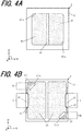
Fig. 4A is a top view illustrating a wiring substrate in the electronic device illustrated inFigs. 3A and 3B . -
Fig. 4B is an internal top view of a wiring substrate in the electronic device illustrated inFigs. 3A and 3B . -
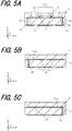
Fig. 5A is a cross-sectional view taken along the line A-A of the electronic device illustrated inFig. 3A . -
Fig. 5B is a cross-sectional view taken along the line B-B of the electronic device illustrated inFig. 3A . -
Fig. 5C is a cross-sectional view taken along the line C-C of the electronic device illustrated inFig. 3A . -
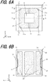
Fig. 6A is a top view illustrating an electronic device according to the third embodiment. -
Fig. 6B is a bottom view ofFig. 6A . -
Fig. 7A is a top view illustrating a wiring substrate in the electronic device illustrated inFigs. 6A and 6B . -
Fig. 7B is an internal top view of a wiring substrate in the electronic device illustrated inFigs. 6A and 6B . -
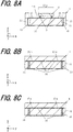
Fig. 8A is a cross-sectional view taken along the line A-A of the electronic device illustrated inFig. 6A . -
Fig. 8B is a cross-sectional view taken along the line B-B of the electronic device illustrated inFig. 6A . -
Fig. 8C is a cross-sectional view taken along the line C-C of the electronic device illustrated inFig. 6A . - Some exemplary embodiments of the present disclosure will be described with reference to the accompanying drawings.
- A
wiring substrate 1 according to the first embodiment, as in examples illustrated inFigs. 1A to 2C , includes an insulatingsubstrate 11, arecess 12 formed in the insulatingsubstrate 11, aninner surface electrode 13 which is located on an inner surface of therecess 12, a viaconductor 14 which is located in a thickness direction of the insulatingsubstrate 11, and awiring conductor 15 which is located on surfaces of the insulatingsubstrate 11 and inside the insulatingsubstrate 11. The insulatingsubstrate 11 has a mounting portion 11a for mounting anelectronic component 2 on a principal surface thereof in the center thereof in a plan view. An electronic device includes thewiring substrate 1 and theelectronic component 2 which is mounted on the mounting portion 11a of thewiring substrate 1. For example, the electronic device is connected, by use of a joining material, to aconnection pad 41 on amodule substrate 4 that constitutes the electronic module. - The
wiring substrate 1 according to the present embodiment includes: the insulatingsubstrate 11 being shaped in a quadrangle in a plan view, including the mounting portion 11a where theelectronic component 2 is mounted on a side of a principal surface of the insulatingsubstrate 11, and having therecess 12 on a side surface thereof; theinner surface electrode 13 which is located on the inner surface of therecess 12; the viaconductor 14 which is located on a corner side of the insulatingsubstrate 11 in a perspective plan view and has both ends located in the thickness direction of the insulatingsubstrate 11; and thewiring conductor 15, on the side of the principal surface of the insulatingsubstrate 11, connecting the mounting portion 11a, theinner surface electrode 13, and the viaconductor 14 with each other. In a perspective plan view, thewiring conductor 15 has a wiring conductor absent region 15a which surrounds a region located between the mounting portion 11a and the viaconductor 14. InFigs. 1A to 2C , an upward direction refers to a positive direction along an imaginary z axis. In the following description, discrimination between the upper and lower sides is merely for convenience, and it is not intended to limit the upper and lower sides when thewiring substrate 1 and other members are practically used. - The
inner surface electrode 13 is indicated in half-tone dot meshing in the examples illustrated inFig. 1A and Fig. 1B . With regard to the viaconductor 14, a region where the side surface of the viaconductor 14 and thewiring conductor 15 overlap is indicated by a dotted line in the examples illustrated inFig. 1A and Fig. 1B . Thewiring conductor 15 is indicated in half-tone dot meshing in the examples illustrated inFig. 1A and Fig. 1B . - The insulating
substrate 11 has a first principal surface (upper surface inFigs. 1A to 2C ), a second principal surface (lower surface inFigs. 1A to 2C ) opposite to the first principal surface, and side surfaces. The insulatingsubstrate 11 is composed of a plurality of insulating layers and has therecess 12 which is located on a side surface thereof in a plan view and which is long in an edge direction. The insulatingsubstrate 11 is shaped in a quadrangle in a plan view, i.e. when viewed from a direction perpendicular to the principal surfaces. The insulatingsubstrate 11 functions as a support body for supporting theelectronic component 2. In the center of the insulatingsubstrate 11, the mounting portion 11a is located for mounting theelectronic component 2 therein in a plan view. - The insulating
substrate 11 may use, for example, ceramics, such as an aluminum oxide sintered body (alumina ceramic), an aluminum nitride sintered body, silicon nitride sintered body, a mullite sintered body, or a glass-ceramic sintered body. In a case where the insulatingsubstrate 11 is, for example, an aluminum oxide sintered body, a slurry is prepared by adding, for example, an appropriate organic binder and a solvent to raw-material powder of, for example, aluminum oxide (Al2O3), silicon oxide (SiO2), magnesium oxide (MgO), or calcium oxide (CaO), and mixing them together. The above slurry is formed in a sheet-like shape by employing a known doctor blade method or a known calendar roll method, so that a ceramic green sheet is formed. Then, the ceramic green sheet is appropriately punched, a plurality of the ceramic green sheets are laminated, so that a green body is formed. The green body is fired at a high temperature (approximately 1400°C), so that an insulatingsubstrate 11 is formed. - The
recess 12 is located on the side surface of the insulatingsubstrate 11 in an edge part of the insulatingsubstrate 11. Therecess 12, as in the examples illustrated inFig. 1A and Fig. 1B , is shaped in a rectangle with arc-shaped corners in a plan view. Therecess 12 may be shaped in a semi-ellipse or a semi-oval or shaped in a rectangle having a plurality of steps, in a plan view. Therecess 12 is formed to be long along the direction of an edge of the insulatingsubstrate 11, and have a width that is larger than a depth thereof. Therecess 12 may be located from one principal surface of the insulatingsubstrate 11 to the other principal surface, or may be located from the middle of the side surface of the insulatingsubstrate 11 to the other principal surface. Theabove recess 12 is formed by forming, in some of ceramic green sheets for the insulatingsubstrate 11, some through holes, which serve as therecess 12, by laser processing, punching with a die, or other processing. - The
inner surface electrode 13, as in the examples illustrated inFigs. 1A to 2C , is located on an inner surface of therecess 12 and is located in the thickness direction of the insulatingsubstrate 11. The viaconductor 14, as in the examples illustrated inFigs. 1A to 2C , is located on a corner side of the insulatingsubstrate 11 and is located in the thickness direction of the insulatingsubstrate 11. Thewiring conductor 15 is located on the principal surfaces of the insulatingsubstrate 11 and inside the insulatingsubstrate 11. Thewiring conductor 15 is located on the principal surfaces of the insulatingsubstrate 11 in the examples illustrated inFigs. 1A to 2C . Theinner surface electrode 13 and the viaconductor 14 are electrically connected to thewiring conductor 15 as in the examples illustrated inFigs. 1A to 2C . Theinner surface electrode 13, the viaconductor 14, and thewiring conductor 15 are the ones for electrically connecting theelectronic component 2 mounted on thewiring substrate 1 with themodule substrate 4 which is provided outside thewiring substrate 1. - The
inner surface electrode 13, the viaconductor 14, and thewiring conductor 15 are made of metallized powder containing tungsten (W), molybdenum (Mo), manganese (Mn), silver (Ag), or copper (Cu). In a case where a refractory metal material such as W or Mo is used, the refractory metal material may be mixed or alloyed with, for example, Cu. - The
inner surface electrode 13 or thewiring conductor 15 is formed by, for example, applying a metallized paste for thewiring conductor 15 on the ceramic green sheet for the insulatingsubstrate 11 by a printing method such as screen printing, and firing the paste together with the ceramic green sheet for the insulatingsubstrate 11. Further, the viaconductor 14 is formed by, for example, punching the ceramic green sheet for the insulatingsubstrate 11 by using a processing method, such as punching with a die or a puncher, or laser processing, to form a through hole for the viaconductor 14, filling the through hole with a metallized paste for the viaconductor 14 by the printing method, and firing the paste with the ceramic green sheet for the insulatingsubstrate 11. The metallized paste is prepared by adding an appropriate solvent and a binder to the above-described metal powder and kneading the mixture so that the viscosity of the mixture is adjusted to an appropriate viscosity. The metallized paste may contain glass powder or ceramic powder to increase the joining strength with respect to the insulatingsubstrate 11. - In a perspective plan view, as in the examples illustrated in
Figs. 1A to 2C , thewiring conductor 15 has the wiring conductor absent region 15a which surrounds a region located between the mounting portion 11a and the viaconductor 14. The wiring conductor absent region 15a, in a perspective plan view, is located on an imaginary line that connects the mounting portion 11a and the viaconductor 14. The wiring conductor absent region 15a of thewiring conductor 15 can be formed by, in applying a metallized paste for thewiring conductor 15 on the ceramic green sheet for the insulatingsubstrate 11 by a printing method such as screen printing, avoiding the metallized paste for thewiring conductor 15 from being applied to the wiring conductor absent region 15a. - Exposed surfaces of the
inner surface electrode 13 and thewiring conductor 15 from the insulatingsubstrate 11 are coated with a metal-plating layer by an electroplating method or an electroless plating method. The metal-plating layer is made of a metal having excellent corrosion resistance and excellent connection member connectivity, such as nickel, copper, gold, or silver. For example, the exposed surfaces of theinner surface electrode 13 and thewiring conductor 15 from the insulatingsubstrate 11 are coated sequentially with a nickel-plating layer having a thickness of about 0.5 µm to 5 µm and a gold-plating layer having a thickness of about 0.1 µm to 3 µm. The above configuration enables effective prevention of corrosion of theinner surface electrode 13 and thewiring conductor 15 and enables strengthening of joining of thewiring conductor 15 to a connectingmember 3 such as a bonding wire and strengthening of joining of theinner surface electrode 13 and thewiring conductor 15 to aconnection pad 41 for connection formed on themodule substrate 4. - The metal-plating layer is not limited to the metal-plating layer including the nickel-plating layer and the gold-plating layer, and may be another metal-plating layer including a nickel-plating layer, a palladium-plating layer, a gold-plating layer, and other layer.
- An electronic device can be fabricated by mounting the
electronic component 2 on the mounting portion 11a which is located in the center of thewiring substrate 1. Theelectronic element 2 mounted on thewiring substrate 1 is a semiconductor element such as an IC chip or an LSI chip; an imaging element such as a charge coupled device (CCD) imaging element and a complementary metal oxide semiconductor (CMOS) imaging element; a light-emitting element such as a laser diode (LD) and a light emitting diode (LED); and a light-receiving element such as a photo diode (PD). For example, in a case where theelectronic component 2 is a flip-chipelectronic component 2, theelectronic component 2 is mounted on thewiring substrate 1 by electrically and mechanically connecting an electrode of theelectronic component 2 with thewiring conductor 15 via a connectingmember 3, such as a solder bump, a gold bump, or an electrically conductive resin (such as an anisotropic electrically-conductive resin). For another example, in a case where theelectronic component 2 is a wire-bonding semiconductor element, the semiconductor element is mounted on thewiring substrate 1 by fixing the semiconductor element onto the mounting portion 11a of thewiring substrate 1 by using a joining member, such as a low-melting brazing material or an electrically conductive resin, and then electrically connecting an electrode of the semiconductor element with thewiring conductor 15 via a connectingmember 3 such as a bonding wire. With the above configuration, theelectronic component 2 is electrically connected to theconductor layer 15. A plurality ofelectronic components 2 may be mounted on the mounting portion 11a of thewiring substrate 1, and, if necessary, a small electronic component such as a resistance element or a capacitance element may be mounted on the mounting portion 11a of thewiring substrate 1. Theelectronic component 2 is sealed with a sealant made of a material such as resin or glass or with, for example, a lid body made of a material such as resin, glass, ceramic, or metal, if necessary. - A plurality of
electronic components 2 may be mounted on the mounting portion 11a of thewiring substrate 1, and, if necessary, a small electronic component, such as a resistance element or a capacitance element, and another component such as a mirror may be mounted around the electronic component(s) 2. In a case where a plurality ofelectronic components 2 are mounted on the mounting portion 11a of thewiring substrate 1, a region surrounding a plurality ofelectronic components 2 in a plan view may be regarded as the mounting portion 11a. Theelectronic component 2 is sealed with a sealant made of a material such as resin or glass or with, for example, a lid body made of a material such as resin, glass, ceramic, or metal if necessary. - The wiring conductor of the electronic device according to the present embodiment is connected to, for example, the
connection pad 41 of themodule substrate 4 via thesolder 5, thereby forming an electronic module. The electronic device is such that theinner surface electrode 13, which is located on the inner surface of therecess 12, and thewiring conductor 15, which is located on the lower surface of thewiring substrate 1, are connected to theconnection pad 41 of themodule substrate 4. - A wiring substrate according to the present embodiment includes: the insulating
substrate 11 being shaped in a quadrangle in a plan view, including the mounting portion 11a where theelectronic component 2 is mounted on a side of a principal surface of the insulatingsubstrate 11, and having therecess 12 on a side surface thereof; theinner surface electrode 13 which is located on the inner surface of therecess 12; the viaconductor 14 which is located on a corner side of the insulatingsubstrate 11 in a perspective plan view and has both ends located in a thickness direction of the insulatingsubstrate 11; and thewiring conductor 15, on the side of the principal surface of the insulatingsubstrate 11, connecting the mounting portion 11a, theinner surface electrode 13, and the viaconductor 14 with each other, wherein, in a perspective plan view, thewiring conductor 15 has a wiring conductor absent region 15a which surrounds a region located between the mounting portion 11a and the viaconductor 14. The above configuration allows heat of theelectronic component 2 transferred through thewiring conductor 15 to be diffused and easily transferred in different directions toward theinner surface electrode 13 and toward the viaconductor 14 and allows heat to be more easily transferred to therecess 12 side, while preventing heat transfer to a viaconductor 14 side. This makes it possible to effectively prevent cracks from being produced between theinner surface electrode 13 and the viaconductor 14, over a long-term use, due to heat transfer to thewiring conductor 15, theinner surface electrode 13, and the viaconductor 14, and application of a current thereto. - Further, a configuration in which, in a perspective plan view, the
wiring conductor 15 is located in a region, on the corner side of the insulatingsubstrate 11, where the viaconductor 14 is located, allows heat transferring in thewiring conductor 15 to be transferred to a side where there are two sides forming the corner of the insulatingsubstrate 11. This makes it possible to effectively prevent cracks from being produced between theinner surface electrode 13 and the viaconductor 14 over a long-term use. - Further, as in the examples illustrated in
Figs. 1A to 2C , in a perspective plan view, theinner surface electrode 13 has a first part I along one edge of the insulatingsubstrate 11, and the first part I and an imaginary extension region N formed by extending the wiring conductor absent region 15a to the side of one edge do not overlap. Since such an arrangement allows theinner surface electrode 13 not to be located between the viaconductor 14 and an outer edge of the insulatingsubstrate 11, it is possible to effectively prevent cracks from being produced between theinner surface electrode 13 and the viaconductor 14 even if the amount of heat transferred to the viaconductor 14 increases over a long-term use. Note that the phrase that the first part I and the imaginary extension region N formed by extending the wiring conductor absent region 15a to the side of one edge do not overlap indicates that, as in the examples illustrated inFigs. 1A to 2C , the wiring conductor absent region 15a, when thewiring substrate 1 is viewed from the side surface thereof, is located on the principal surface of the insulatingsubstrate 11 between the corner of thewiring substrate 1 and acutout 12 thereof and does not overlap theinner surface electrode 13. - Further, on the opposite side with respect to the mounting portion 11a from the
recess 12, theinner surface electrode 13, the via conductor 14 (first via conductor), the wiring conductor 15 (first wiring conductor), and the wiring conductor absent region 15a (first wiring conductor absent region 15a), are located anotherrecess 12, anotherinner surface electrode 13, another via conductor 14 (second via conductor), another wiring conductor 15 (second wiring conductor), and another wiring conductor absent region 15a (second wiring conductor absent region 15a). This prevents heat of theelectronic component 2 transferred through thewiring conductor 15 to be transferred to the via conductors 14 (first via conductor and second via conductor), which are located at positions far from each other. This makes it possible to effectively prevent cracks from being produced between theinner surface electrode 13 and the viaconductor 14 over a long-term use. - Further, the thermal conductivity of the
inner surface electrode 13 may be made higher than the thermal conductivity of the viaconductor 14. The above arrangement allows heat to be more easily transferred to theinner surface electrode 13 side on therecess 12 side, while preventing heat transfer to the viaconductor 14 side. This makes it possible to effectively prevent cracks from being produced between theinner surface electrode 13 and the viaconductor 14, over a long-term use, due to heat transfer to thewiring conductor 15, theinner surface electrode 13, and the viaconductor 14 and application of a current thereto. The thermal conductivity of theinner surface electrode 13 may be made higher than the thermal conductivity of the viaconductor 14, by arranging theinner surface electrode 13 and the viaconductor 14, for example, such that theinner surface electrode 13 is a metal conductor made of copper, or a mixed metal conductor made of copper and tungsten or molybdenum, and the viaconductor 14 is a metal conductor made of tungsten or molybdenum. Alternatively, the thermal conductivity of theinner surface electrode 13 may be made higher than the thermal conductivity of the viaconductor 14 by setting the content of the glass powder and ceramic powder contained in theinner surface electrode 13 to be lower than the content of the glass powder and ceramic powder contained in the viaconductor 14. - The electronic device includes the
wiring substrate 1 having the above-described configuration and theelectronic component 2 mounted on thewiring substrate 1. This allows the electronic device to be a compact, highly functional electronic device having excellent long-term reliability. - The electronic module includes: the
module substrate 4 having theconnection pad 41; and the electronic device having the above-described configuration and being connected to theconnection pad 41 via thesolder 5. The configuration in which the electronic module has the device and themodule substrate 4 to which the electronic device is connected allows the electronic module to have excellent long-term reliability. - Next, a
wiring substrate 1 according to the second embodiment will be described with reference toFigs. 3A to 5C . - The
wiring substrate 1 according to the second embodiment differs from thewiring substrate 1 according to the above-described embodiment in that a plurality of viaconductors 14 are located along an outer edge of a wiring conductor absent region 15a in a perspective plan view. - The
inner surface electrode 13 is indicated in half-tone dot meshing in the examples illustrated inFig. 3B andFig. 4B . With regard to the viaconductors 14, regions where the side surfaces of the viaconductors 14 and awiring conductor 15 overlap are indicated by a dotted line in the examples illustrated inFig. 3B andFig. 4B . Thewiring conductor 15 is indicated in half-tone dot meshing in the examples illustrated inFig. 3A andFig. 4B . - The
wiring substrate 1 according to the second embodiment, as in the case of thewiring substrate 1 according to the above-described embodiment, allows heat of theelectronic component 2 transferred through thewiring conductor 15 to be diffused and easily transferred in different directions toward theinner surface electrode 13 and toward the viaconductor 14 and allows heat to be more easily transferred to therecess 12 side, while preventing heat transfer to the viaconductor 14 side. This makes it possible to effectively prevent cracks from being produced between theinner surface electrode 13 and the viaconductor 14, over a long-term use, due to heat transfer to thewiring conductor 15, theinner surface electrode 13, and the viaconductor 14, and application of a current thereto. - Further, a configuration in which, in a perspective plan view, each of the via
conductors 14 is located on a corresponding one of sides where edges forming corners of the insulatingsubstrate 11 are provided disperses heat transfer from thewiring conductor 15 to the viaconductor 14 side. This makes it possible to effectively prevent cracks from being produced between theinner surface electrode 13 and the viaconductor 14 over a long-term use. - Further, a configuration in which a plurality of via
conductors 14 are located along the outer edge of the wiring conductor absent region 15a disperses heat transfer to the sides of the individual viaconductors 14, allows heat transfer to the sides of the viaconductors 14 through thewiring conductor 15 along the outer edge of the wiring conductor absent region 15a to be more easily dispersed, and prevents heat transfer to the viaconductors 14 sides each of which is close to therecess 12 side. This makes it possible to effectively prevent cracks from being produced between theinner surface electrode 13 and the viaconductor 14 over a long-term use. - Further, in the examples illustrated in
Figs. 3A to 5C , two viaconductors 14 are located along the outer edge of the wiring conductor absent region 15a. Three or more viaconductors 14 may be located along the outer edge of the wiring conductor absent region 15a. - Further, in a case where the plurality of via
conductors 14 are located along the outer edge of the wiring conductor absent region 15a, as in the examples illustrated inFigs. 3A to 5C , the viaconductors 14 on one side where therecess 12, theinner surface electrode 13, the viaconductor 14, thewiring conductor 15, and the wiring conductor absent region 15a are located may be equal in number to the viaconductors 14 on the other side, opposite to the one side with respect to the mounting portion 11a, where therecess 12, theinner surface electrode 13, the viaconductor 14, thewiring conductor 15, and the wiring conductor absent region 15a are located. - Further, the
wiring substrate 1 has, on an upper surface thereof, acavity 16 for accommodating anelectronic component 2. In the above configuration, the wiring conductor absent region 15a of thewiring conductor 15, as in the examples illustrated inFigs. 3A to 5C , may be such that, in a plan view, a portion of the wiring conductor absent region 15a is located inward of the inner surface of thecavity 16 and is exposed. A configuration, as in the above configuration, in which a portion of the wiring conductor absentregion 15 of thewiring conductor 15 is exposed provides good lamination of an upper surface-side layer of the insulatingsubstrate 11 and a lower surface-side layer thereof at the corners of thecavity 16, provides good heat transfer to side-wall sides of thecavity 16 in the vicinity of the wiring conductor absentregion 15, and prevents heat transfer to the viaconductor 14 side. This makes it possible to effectively prevent cracks from being produced between theinner surface electrode 13 and the viaconductor 14, over a long-term use. - Except for the points described above, the
wiring substrate 1 according to the second embodiment can be manufactured by using a manufacturing method which is the same as the manufacturing method of thewiring substrate 1 according to the above-described embodiment. - Next, a
wiring substrate 1 according to the third embodiment will be described with reference toFigs. 6A to 8C . - The
wiring substrate 1 according to the third embodiment differs from thewiring substrate 1 according to the above-described embodiment in that, in a perspective plan view, viaconductors 14 are located, on a one-to-one basis, on four corner sides of the insulatingsubstrate 11 and that thewiring conductor 15 has a wiring conductor absent region 15a which surrounds a region located between the mounting portion 11a and the viaconductors 14. - The
inner surface electrode 13 is indicated in half-tone dot meshing in the examples illustrated inFig. 6B andFig. 7B . With regard to the viaconductors 14, regions where the side surfaces of the viaconductors 14 and thewiring conductor 15 overlap are indicated by a dotted line in the examples illustrated inFig. 6B andFig. 7B . Thewiring conductor 15 is indicated in half-tone dot meshing in the examples illustrated inFigs. 6A to 7B . - The
wiring substrate 1 according to the third embodiment, as in the case of thewiring substrate 1 according to the above-described embodiments, allows heat of theelectronic component 2 transferred through thewiring conductor 15 to be diffused and easily transferred in different directions toward theinner surface electrode 13 and toward the viaconductor 14 and allows heat to be more easily transferred to therecess 12 side, while preventing heat transfer to the viaconductor 14 side. This makes it possible to effectively prevent cracks from being produced between theinner surface electrode 13 and the viaconductor 14, over a long-term use, due to heat transfer to thewiring conductor 15, theinner surface electrode 13, and the viaconductor 14 and application of a current thereto. - Further, a configuration in which the via
conductors 14 and wiring conductor absent regions 15a of thewiring conductor 15 are each located, on a one-to-one basis, at four corners of thewiring substrate 1, allows heat to be diffused and easily transferred in different directions toward the four viaconductors 14, and, while preventing heat transfer to the sides of the individual viaconductors 14, makes it possible to effectively prevent cracks from being produced between theinner surface electrode 13 and the viaconductors 14, over a long-term use, due to heat transfer to thewiring conductor 15, theinner surface electrode 13, and the viaconductors 14, and application of a current thereto. - Except for the points described above, the
wiring substrate 1 according to the third embodiment can be manufactured by using a manufacturing method which is the same as the manufacturing method of thewiring substrate 1 according to the above-described embodiments. - The present disclosure is not limited to the examples of the above-described embodiments, and various modifications can be made. For example, the insulating
substrate 11 may be shaped in a rectangle having a recess or a chamfer on the side surfaces thereof or at the corners thereof in a plan view. - The
wiring substrate 1 according to the second embodiment and thewiring substrate 1 according to the third embodiment are such that, in a vertical cross-sectional view, the inner surface of thecavity 16 is formed to be perpendicular to the upper surface of the insulatingsubstrate 11. Alternatively, the inner surface of thecavity 16 may be inclined so that an opening side of thecavity 16 is wider than a bottom surface side of thecavity 16. - Further, the
wiring substrates 1 according to the first to third embodiments may be each combined with the configuration(s) of any of the other embodiment(s). For example, thewiring substrate 1 according to the first embodiment, as in the case of thewiring substrate 1 according to the third embodiment, may be such that the viaconductor 14 and the wiring conductor absent region 15a of thewiring conductor 15 are each located on each of the sides of the four corners of thewiring substrate 1. - Further, the
wiring substrate 1 according to the first embodiment, as in the case of thewiring substrate 1 according to the second embodiment and thewiring substrate 1 according to the third embodiment, may include the cavity 17. - Further, the
wiring substrate 1 may be manufactured in the form of a multi-piece substrate.
Claims (7)
- A wiring substrate comprising:an insulating substrate being shaped in a quadrangle in a plan view, including a mounting portion where an electronic component is mounted on a side of a principal surface of the insulating substrate, and having a recess on a side surface thereof;an inner surface electrode which is located on an inner surface of the recess;a via conductor which is located on a corner side of the insulating substrate in a perspective plan view and has both ends located in a thickness direction of the insulating substrate; anda wiring conductor, on the side of the principal surface of the insulating substrate, connecting the mounting portion, the inner surface electrode, and the via conductor with each other,wherein, in a perspective plan view, the wiring conductor has a wiring conductor absent region which surrounds a region located between the mounting portion and the via conductor.
- The wiring substrate according to claim 1, wherein in a perspective plan view, the wiring conductor is located in a region, on the corner side of the insulating substrate, where the via conductor is located.
- The wiring substrate according to claim 1 or 2, whereinin a perspective plan view, the inner surface electrode has a first part along one edge of the insulating substrate, andthe first part and an imaginary extension region formed by extending the wiring conductor absent region to a side of the one edge do not overlap.
- The wiring substrate according to any one of claims 1 to 3, wherein
in a perspective plan view, the via conductor is located on each of sides where edges forming corners of the insulating substrate are provided. - The wiring substrate according to any one of claims 1 to 4, wherein
on an opposite side with respect to the mounting portion from the recess, the inner surface electrode, the via conductor, the wiring conductor, and the wiring conductor absent region, are located another recess, another inner surface electrode, another via conductor, another wiring conductor, and another wiring conductor absent region. - An electronic device comprising:a wiring substrate according to any one of claims 1 to 5; andan electronic component mounted on the wiring substrate.
- An electronic module comprising:a module substrate having a connection pad; andan electronic device according to claim 6 connected to the connection pad via a solder.
Applications Claiming Priority (2)
| Application Number | Priority Date | Filing Date | Title |
|---|---|---|---|
| JP2018242957 | 2018-12-26 | ||
| PCT/JP2019/042862 WO2020137152A1 (en) | 2018-12-26 | 2019-10-31 | Wiring substrate, electronic device, and electronic module |
Publications (2)
| Publication Number | Publication Date |
|---|---|
| EP3905314A1 true EP3905314A1 (en) | 2021-11-03 |
| EP3905314A4 EP3905314A4 (en) | 2022-02-16 |
Family
ID=71128953
Family Applications (1)
| Application Number | Title | Priority Date | Filing Date |
|---|---|---|---|
| EP19905747.2A Pending EP3905314A4 (en) | 2018-12-26 | 2019-10-31 | WIRING SUBSTRATE, ELECTRONIC DEVICE AND ELECTRONIC MODULE |
Country Status (5)
| Country | Link |
|---|---|
| US (1) | US11742278B2 (en) |
| EP (1) | EP3905314A4 (en) |
| JP (1) | JP7136926B2 (en) |
| CN (1) | CN113228258B (en) |
| WO (1) | WO2020137152A1 (en) |
Families Citing this family (1)
| Publication number | Priority date | Publication date | Assignee | Title |
|---|---|---|---|---|
| FR3136888B1 (en) * | 2022-06-16 | 2025-06-20 | St Microelectronics Grenoble 2 | Integrated circuit packages |
Family Cites Families (6)
| Publication number | Priority date | Publication date | Assignee | Title |
|---|---|---|---|---|
| JP2005191097A (en) * | 2003-12-24 | 2005-07-14 | Kawaguchiko Seimitsu Co Ltd | Semiconductor package |
| JP5942594B2 (en) | 2012-04-06 | 2016-06-29 | 日亜化学工業株式会社 | Semiconductor device |
| CN105359632B (en) * | 2013-10-23 | 2018-02-06 | 京瓷株式会社 | Circuit board and electronic installation |
| US10319672B2 (en) * | 2015-06-25 | 2019-06-11 | Kyocera Corporation | Wiring board, electronic device, and electronic module |
| JP6791719B2 (en) | 2016-10-26 | 2020-11-25 | 京セラ株式会社 | Substrate for mounting electronic components, electronic devices and electronic modules |
| US11145587B2 (en) * | 2017-05-26 | 2021-10-12 | Kyocera Corporation | Electronic component mounting substrate, electronic device, and electronic module |
-
2019
- 2019-10-31 CN CN201980085080.6A patent/CN113228258B/en active Active
- 2019-10-31 JP JP2020562873A patent/JP7136926B2/en active Active
- 2019-10-31 WO PCT/JP2019/042862 patent/WO2020137152A1/en not_active Ceased
- 2019-10-31 US US17/417,413 patent/US11742278B2/en active Active
- 2019-10-31 EP EP19905747.2A patent/EP3905314A4/en active Pending
Also Published As
| Publication number | Publication date |
|---|---|
| EP3905314A4 (en) | 2022-02-16 |
| WO2020137152A1 (en) | 2020-07-02 |
| JPWO2020137152A1 (en) | 2021-10-21 |
| CN113228258B (en) | 2024-08-27 |
| US11742278B2 (en) | 2023-08-29 |
| JP7136926B2 (en) | 2022-09-13 |
| US20220077049A1 (en) | 2022-03-10 |
| CN113228258A (en) | 2021-08-06 |
Similar Documents
| Publication | Publication Date | Title |
|---|---|---|
| US11145587B2 (en) | Electronic component mounting substrate, electronic device, and electronic module | |
| US11930586B2 (en) | Wiring substrate, electronic device and electronic module | |
| CN111033771B (en) | Substrates for mounting electronic components, electronic devices and electronic modules | |
| JP2023071984A (en) | Wiring boards, electronic devices and electronic modules | |
| US11784117B2 (en) | Wiring board, electronic device, and electronic module | |
| JP6626735B2 (en) | Electronic component mounting board, electronic device and electronic module | |
| US11742278B2 (en) | Wiring substrate, electronic device, and electronic module | |
| EP3370254B1 (en) | Wiring substrate, electronic device and electronic module | |
| US11024554B2 (en) | Wiring substrate, electronic device, and electronic module | |
| JP6687435B2 (en) | Wiring board, electronic device and electronic module | |
| JP2021158253A (en) | Substrate for mounting electronic components, electronic devices and electronic modules | |
| JP6595308B2 (en) | Electronic component mounting substrate, electronic device and electronic module |
Legal Events
| Date | Code | Title | Description |
|---|---|---|---|
| STAA | Information on the status of an ep patent application or granted ep patent |
Free format text: STATUS: THE INTERNATIONAL PUBLICATION HAS BEEN MADE |
|
| PUAI | Public reference made under article 153(3) epc to a published international application that has entered the european phase |
Free format text: ORIGINAL CODE: 0009012 |
|
| STAA | Information on the status of an ep patent application or granted ep patent |
Free format text: STATUS: REQUEST FOR EXAMINATION WAS MADE |
|
| 17P | Request for examination filed |
Effective date: 20210621 |
|
| AK | Designated contracting states |
Kind code of ref document: A1 Designated state(s): AL AT BE BG CH CY CZ DE DK EE ES FI FR GB GR HR HU IE IS IT LI LT LU LV MC MK MT NL NO PL PT RO RS SE SI SK SM TR |
|
| REG | Reference to a national code |
Ref country code: DE Ref legal event code: R079 Free format text: PREVIOUS MAIN CLASS: H01L0023120000 Ipc: H01L0023130000 |
|
| A4 | Supplementary search report drawn up and despatched |
Effective date: 20220118 |
|
| RIC1 | Information provided on ipc code assigned before grant |
Ipc: H05K 1/11 20060101ALI20220112BHEP Ipc: H01L 23/367 20060101ALI20220112BHEP Ipc: H01L 23/498 20060101ALI20220112BHEP Ipc: H01L 23/13 20060101AFI20220112BHEP |
|
| DAV | Request for validation of the european patent (deleted) | ||
| DAX | Request for extension of the european patent (deleted) | ||
| P01 | Opt-out of the competence of the unified patent court (upc) registered |
Effective date: 20230505 |