EP3904896B1 - Elektrische schaltungsanordnung und verfahren zur funktionsprüfung eines überwachungsgeräts für ein elektrisches stromversorgungssystem - Google Patents
Elektrische schaltungsanordnung und verfahren zur funktionsprüfung eines überwachungsgeräts für ein elektrisches stromversorgungssystem Download PDFInfo
- Publication number
- EP3904896B1 EP3904896B1 EP21169290.0A EP21169290A EP3904896B1 EP 3904896 B1 EP3904896 B1 EP 3904896B1 EP 21169290 A EP21169290 A EP 21169290A EP 3904896 B1 EP3904896 B1 EP 3904896B1
- Authority
- EP
- European Patent Office
- Prior art keywords
- voltage
- transistor
- control
- actual
- resistance value
- Prior art date
- Legal status (The legal status is an assumption and is not a legal conclusion. Google has not performed a legal analysis and makes no representation as to the accuracy of the status listed.)
- Active
Links
Images


Classifications
-
- G—PHYSICS
- G01—MEASURING; TESTING
- G01R—MEASURING ELECTRIC VARIABLES; MEASURING MAGNETIC VARIABLES
- G01R31/00—Arrangements for testing electric properties; Arrangements for locating electric faults; Arrangements for electrical testing characterised by what is being tested not provided for elsewhere
- G01R31/40—Testing power supplies
-
- G—PHYSICS
- G01—MEASURING; TESTING
- G01R—MEASURING ELECTRIC VARIABLES; MEASURING MAGNETIC VARIABLES
- G01R35/00—Testing or calibrating of apparatus covered by the other groups of this subclass
-
- G—PHYSICS
- G01—MEASURING; TESTING
- G01R—MEASURING ELECTRIC VARIABLES; MEASURING MAGNETIC VARIABLES
- G01R31/00—Arrangements for testing electric properties; Arrangements for locating electric faults; Arrangements for electrical testing characterised by what is being tested not provided for elsewhere
-
- G—PHYSICS
- G01—MEASURING; TESTING
- G01R—MEASURING ELECTRIC VARIABLES; MEASURING MAGNETIC VARIABLES
- G01R19/00—Arrangements for measuring currents or voltages or for indicating presence or sign thereof
- G01R19/165—Indicating that current or voltage is either above or below a predetermined value or within or outside a predetermined range of values
-
- G—PHYSICS
- G01—MEASURING; TESTING
- G01R—MEASURING ELECTRIC VARIABLES; MEASURING MAGNETIC VARIABLES
- G01R27/00—Arrangements for measuring resistance, reactance, impedance, or electric characteristics derived therefrom
- G01R27/02—Measuring real or complex resistance, reactance, impedance, or other two-pole characteristics derived therefrom, e.g. time constant
- G01R27/025—Measuring very high resistances, e.g. isolation resistances, i.e. megohm-meters
-
- G—PHYSICS
- G01—MEASURING; TESTING
- G01R—MEASURING ELECTRIC VARIABLES; MEASURING MAGNETIC VARIABLES
- G01R27/00—Arrangements for measuring resistance, reactance, impedance, or electric characteristics derived therefrom
- G01R27/02—Measuring real or complex resistance, reactance, impedance, or other two-pole characteristics derived therefrom, e.g. time constant
- G01R27/16—Measuring impedance of element or network through which a current is passing from another source, e.g. cable, power line
-
- G—PHYSICS
- G01—MEASURING; TESTING
- G01R—MEASURING ELECTRIC VARIABLES; MEASURING MAGNETIC VARIABLES
- G01R31/00—Arrangements for testing electric properties; Arrangements for locating electric faults; Arrangements for electrical testing characterised by what is being tested not provided for elsewhere
- G01R31/12—Testing dielectric strength or breakdown voltage ; Testing or monitoring effectiveness or level of insulation, e.g. of a cable or of an apparatus, for example using partial discharge measurements; Electrostatic testing
- G01R31/1227—Testing dielectric strength or breakdown voltage ; Testing or monitoring effectiveness or level of insulation, e.g. of a cable or of an apparatus, for example using partial discharge measurements; Electrostatic testing of components, parts or materials
- G01R31/1263—Testing dielectric strength or breakdown voltage ; Testing or monitoring effectiveness or level of insulation, e.g. of a cable or of an apparatus, for example using partial discharge measurements; Electrostatic testing of components, parts or materials of solid or fluid materials, e.g. insulation films, bulk material; of semiconductors or LV electronic components or parts; of cable, line or wire insulation
- G01R31/1272—Testing dielectric strength or breakdown voltage ; Testing or monitoring effectiveness or level of insulation, e.g. of a cable or of an apparatus, for example using partial discharge measurements; Electrostatic testing of components, parts or materials of solid or fluid materials, e.g. insulation films, bulk material; of semiconductors or LV electronic components or parts; of cable, line or wire insulation of cable, line or wire insulation, e.g. using partial discharge measurements
-
- G—PHYSICS
- G01—MEASURING; TESTING
- G01R—MEASURING ELECTRIC VARIABLES; MEASURING MAGNETIC VARIABLES
- G01R31/00—Arrangements for testing electric properties; Arrangements for locating electric faults; Arrangements for electrical testing characterised by what is being tested not provided for elsewhere
- G01R31/50—Testing of electric apparatus, lines, cables or components for short-circuits, continuity, leakage current or incorrect line connections
- G01R31/52—Testing for short-circuits, leakage current or ground faults
-
- G—PHYSICS
- G01—MEASURING; TESTING
- G01R—MEASURING ELECTRIC VARIABLES; MEASURING MAGNETIC VARIABLES
- G01R27/00—Arrangements for measuring resistance, reactance, impedance, or electric characteristics derived therefrom
- G01R27/02—Measuring real or complex resistance, reactance, impedance, or other two-pole characteristics derived therefrom, e.g. time constant
- G01R27/16—Measuring impedance of element or network through which a current is passing from another source, e.g. cable, power line
- G01R27/18—Measuring resistance to earth, i.e. line to ground
-
- H—ELECTRICITY
- H02—GENERATION; CONVERSION OR DISTRIBUTION OF ELECTRIC POWER
- H02M—APPARATUS FOR CONVERSION BETWEEN AC AND AC, BETWEEN AC AND DC, OR BETWEEN DC AND DC, AND FOR USE WITH MAINS OR SIMILAR POWER SUPPLY SYSTEMS; CONVERSION OF DC OR AC INPUT POWER INTO SURGE OUTPUT POWER; CONTROL OR REGULATION THEREOF
- H02M3/00—Conversion of DC power input into DC power output
- H02M3/02—Conversion of DC power input into DC power output without intermediate conversion into AC
- H02M3/04—Conversion of DC power input into DC power output without intermediate conversion into AC by static converters
- H02M3/10—Conversion of DC power input into DC power output without intermediate conversion into AC by static converters using discharge tubes with control electrode or semiconductor devices with control electrode
- H02M3/145—Conversion of DC power input into DC power output without intermediate conversion into AC by static converters using discharge tubes with control electrode or semiconductor devices with control electrode using devices of a triode or transistor type requiring continuous application of a control signal
- H02M3/155—Conversion of DC power input into DC power output without intermediate conversion into AC by static converters using discharge tubes with control electrode or semiconductor devices with control electrode using devices of a triode or transistor type requiring continuous application of a control signal using semiconductor devices only
Definitions
- the invention relates to an electrical circuit arrangement and a method for functional testing of a monitoring device for an electrical power supply system, with a test resistor which can be connected between an active conductor of the power supply system and earth and has an adjustable actual resistance value.
- the invention further relates to a modular circuit arrangement consisting of several electrical circuit arrangements according to the invention.
- an insulation monitoring device IMD
- RCM residual current monitoring device
- monitoring devices must therefore be checked to ensure that they function in accordance with standards by means of initial commissioning tests and throughout the entire period of use in recurring tests with specified test intervals.
- Measuring methods for determining the insulation resistance in unearthed power supply systems are based in principle on the superposition of a measuring voltage generated in the insulation monitoring device, so that a measuring current proportional to the insulation fault (fault resistance) is established, which causes a corresponding voltage drop across a measuring resistor of the insulation monitoring device. If the voltage drop exceeds a certain value as a result of a reduced insulation resistance and thus a higher measuring current, a message is triggered.
- test resistor with a defined resistance value is inserted as a fault resistor into the network monitored by the insulation monitoring device between one or more active conductors and earth.
- a differential current monitoring device in grounded power supply systems is based on the fact that when the electrical system is operating correctly, the vectorial sum of the currents on all active conductors of a supply line is equal to zero and therefore there is no magnetic field in a magnetizable ring core of a measuring current transformer surrounding the supply line Residual current monitoring device exists. If an insulation fault results in a fault current that flows outside the supply line via a body or via earth, a differential current results. The changing magnetic field of this differential current induces a voltage in a secondary coil of the measuring current transformer, which triggers an alarm signal if a preselected value of the differential current is exceeded.
- test resistor with a defined resistance value must be connected as a fault resistor, which generates an artificial fault current that is "passed" past the toroidal core of the residual current monitoring device.
- testing device is known from the company Gossen Metrawatt (http://www.gmc-instuments.de/media/de/product_manual/profi-test-master-seculifeip-iq-ba_d.pdf), which is used for functional testing of the insulation monitoring device, single-phase faults can be generated with discrete resistance values and manual tripping time recording.
- fault plugs available on the market that connect a built-in fault resistor to ground.
- electrically unsafe resistance decades are used to generate errors.
- the present invention is therefore based on the object of creating an electrical circuit arrangement and a method for functional testing of a monitoring device for a power supply system, in particular an insulation monitoring device and a residual current monitoring device.
- the technical teaching according to the invention should be (technically) flexibly adaptable to the measuring environment and the measuring task, whereby the electrical circuit arrangement should also be able to be manufactured inexpensively and used flexibly (economically) in terms of size and weight.
- the inventive idea realized by the invention is, firstly, to use a bidirectional cascade consisting of field effect transistors as a test resistor instead of discrete ohmic resistors, whereby the field effect transistors are not used as switches, as is usual in technical terms, but as a variable ohmic resistor.
- the bidirectional cascade consists of a series connection of two field effect transistors arranged in mirror image.
- the field effect transistors In power operation, the field effect transistors cannot be operated in the linear operating range, but almost exclusively in the saturation range. Therefore, the field effect transistor cascade is forced by an analog control loop into an ohmic behavior in saturation operation and, due to the bidirectionality, works in the first and third quadrants of a characteristic field of the field effect transistor cascade. This means that both direct voltage and alternating voltage operation is possible.
- a second core element of the invention is the analog control using a control loop for continuous adjustment of the resistance value for the test resistor.
- the resistance value of the bidirectional cascade consisting of field effect transistors in a closed circuit is regulated to a predeterminable resistance setpoint.
- the control circuit controls the field effect transistors in their characteristic field so that an ohmic resistance characteristic is created.
- the combination of the field effect transistor cascade and its analog control according to the invention forms a value-continuous equivalent to a discretely variable setting of the resistance value.
- the continuous adjustment of the resistance values enables a value and time-continuous (error) resistance curve to test the monitoring function, in which real system behavior can be simulated.
- the test resistor designed as a bidirectional transistor cascade with the variable resistance value as a controlled variable, forms the controlled system of the control loop.
- the bidirectional transistor cascade is preceded by a transistor driver circuit, which is controlled by the manipulated variable provided by the controller.
- the controller in turn generates the manipulated variable from the difference voltage that is generated in the comparison element.
- the differential voltage represents the control deviation between the target voltage and the actual voltage, whereby the voltage measurement records the transistor voltage that drops across the transistor cascade and returns it to the comparison element as the actual voltage in a scaled manner.
- the target voltage is determined as a reference variable from a predeterminable target resistance value using the actual current in the transformation block.
- the current measurement determines the transistor current flowing through the transistor cascade and, scaled, is fed to the transformation block as the actual current.
- the control is given a setpoint of the resistance value.
- the desired resistance value is set in the control loop by means of feedback from the current measurement of the transistor current flowing in the transistor cascade and by means of feedback from the voltage measurement of the transistor voltage dropping across the transistor cascade.
- test resistor i.e. the bidirectional transistor cascade
- the conductor-to-earth voltage acts as a disturbance variable acting on the controlled system, so that the manipulated variable is continuously updated to maintain the resistance setpoint in an AC power supply system must become.
- the manipulated variable for a given resistance setpoint would be constant.
- the control is switched off by pulling the actual voltage - the output of the voltage measurement - to ground potential.
- the PI controller (see below) will reduce the control deviation by reducing the manipulated variable until this control deviation is constantly zero.
- control deviation is initially negative due to the missing actual current.
- the PI controller then follows this by continuously increasing the manipulated variable until the control deviation is back to zero.
- the electrical circuit arrangement has a microcontroller for specifying the resistance setpoint via a digital setting element and for controlling the switching device by means of a switching signal.
- the resistance setpoint is specified in digital form via the microcontroller and forwarded as an analog signal to the input of the transformation block via the digital setting element.
- the digital adjustment element can be designed, for example, as a digital potentiometer or as a digital-to-analog converter.
- the microcontroller provides a switching signal, which is supplied to the switching device directly or, linked to other signals (overcurrent signal, overtemperature signal), via a digital circuit.
- the microcontroller is advantageously configured to specify an amplitude-modulated resistance pattern from temporally successive resistance setpoints.
- the microcontroller can be set up to specify a defined time sequence of different resistance setpoints, which is recognized by the monitoring device as a signal sequence (residual current signature) when detecting the residual current in order to achieve a specific to trigger action.
- this resistance pattern can be interpreted as a start signal for a test phase.
- the electrical circuit arrangement has an overtemperature detector for detecting an overtemperature of the transistor cascade and an overcurrent detector for detecting an overload value of the actual current, an overtemperature signal and an overcurrent signal being transmitted via a digital circuit with an output signal of the Microcontroller for controlling the switching device are linked by means of the switching signal.
- the reliability of the electrical circuit arrangement according to the invention is thus ensured by safety shutdowns in the event of overcurrent and/or overtemperature of the transistor cascade.
- the digital circuit is preferably designed as an RS flip-flop.
- the digital circuit Since the control should be switched off using the safety functions of overcurrent and overtemperature detection, regardless of the switching signal from the microcontroller, the digital circuit is designed as an RS flip-flop. Setting the RS flip-flop, i.e. switching on the control, can only be done by the microcontroller. Resetting the RS flip-flop, i.e. switching off the control, can be done by ORing the overcurrent signal, overtemperature signal and an output signal from the microcontroller.
- the controller is preferably designed as a PI controller.
- a PI controller is used as a controller in the control system, which, in addition to its proportional behavior (P component), has a superimposed integral component and therefore does not lead to any permanent control deviation.
- circuit arrangements according to the invention are combined in a modular circuit arrangement, each of the electrical circuit arrangements being assigned a different active conductor of the electrical power supply system and a central control unit for controlling and monitoring the electrical circuit arrangements being implemented.
- the electrical circuit arrangement according to the invention consisting of the transistor cascade and the control, can be viewed as a module which can be duplicated several times in order to be able to imprint error resistors (test resistors) with different values at different points in the power supply system at the same time.
- the electrical circuit arrangement according to the invention is therefore required three times and is each connected to a different active conductor. This option ideally also covers the testing of the normative requirement for detecting symmetrical insulation faults.
- the modular circuit arrangement has a central control unit that outputs the desired resistance setpoints to the modules and monitors their function.
- a communication connection is provided between the central control unit and the monitoring device to be tested.
- data can be exchanged in both directions between the central control unit of the modular circuit arrangement and the monitoring device, for example to receive reporting signals from the monitoring device to be tested or to activate precise trigger time measurement.
- the monitoring device to be tested can be informed via the communication connection based on the modular circuit arrangement that a test should be initiated.
- the communication connection can be wired or wireless.
- the previously described electrical circuit arrangement according to the invention is based on a method for functional testing of a monitoring device for an electrical power supply system, in which a test resistor with an adjustable resistance value is connected between an active conductor of the power supply system and earth.
- the test resistor is designed as a bidirectional cascade of field effect transistors and the resistance value is set to a predeterminable resistance setpoint value continuously using an analog control system.
- the resistance value is set to a predeterminable resistance setpoint value continuously using an analog control and thus enables flexible adaptation to the system environment and to test specifications with a minimized size and material expenditure.
- the method can also be used in combination with a central control unit in a modular circuit arrangement for a multi-phase power supply system in such a way that an adapted test resistor is assigned to several active conductors.
- the respective active conductor is equipped with an inventive Circuit arrangement is connected and a test resistor with a defined resistance value is individually set.
- Fig. 1 shows a state-of-the-art test arrangement with variable test resistors for functional testing of an insulation monitoring device 4 installed in an ungrounded power supply system 2.
- the power supply system 2 has two active conductors L1, L2, to which a consumer R L is connected.
- the insulation monitoring device 4 is connected to the active conductors L1, L2 and earth (earth potential) PE for insulation resistance measurement (measuring the fault resistance in the power supply system 2).
- variable test resistors R f1 , R f2 are arranged between an active conductor L1, L2 and earth PE, via which the conductor-earth voltage U L1-PE , U L2-PE drops.
- a closed measuring circuit is formed via an active conductor L1, L2, the test resistors R f1 , R f2 and earth PE back to the insulation monitoring device 4, in which a fault current (measuring current) flows which flows in the insulation monitoring device 4 can be evaluated.
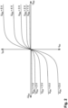
- Fig. 2 A characteristic field of the bidirectional MOSFET transistor cascade is shown.
- MOSFETs are preferably used as transistors. Depending on the control voltage U GS , a certain current I DD flowing across the cascade is established when the voltage U DD is applied across the transistor cascade.
- the bidirectional transistor cascade 12 consists of a series connection of two MOSFET transistors arranged in mirror image, so that working areas of the transistor cascade 12 result in the first and third quadrants of the characteristic curve field.
- the analog regulation 10 Fig. 3
- the transistor cascade 12 is forced into ohmic behavior.
- Fig. 3 shows the electrical circuit arrangement 20 according to the invention with bidirectional transistor cascade 12 and control 10.
- the desired resistance setpoint R 0 is initially specified as the input variable of the control system 10, which is transformed into the setpoint voltage U 0 via the transformation block 22.
- the transformation takes place via the current measurement 25, which corresponds to the transistor current I m (corresponds to I DD in) flowing via the transistor cascade 12 Fig. 2 ) is recorded and scaled (k 2 ) as the actual current I x to the transformation block 22.
- the target voltage U 0 and the actual voltage U x which are obtained via the voltage measurement 26 from the transistor voltage U m dropping across the transistor cascade 12, and scaled (k 1 ), a differential voltage U d is formed.
- the differential voltage U d is fed to the controller 40 - which is preferably a PI controller - which uses it to form a manipulated variable W for controlling the transistor cascade 12.
- the transistor cascade 12 includes a driver circuit 16 for controlling the transistor path 14.
- the control 10 causes the actual resistance value R x of the transistor path 14 of the transistor cascade 12 to adjust to the predetermined resistance setpoint R 0 .
- a switching device 27 is provided between the voltage measurement 26 and the comparison element 24, which sets the actual voltage U x to the value zero (ground potential). pulls.
- the switching device 27 can be controlled directly by means of a switching signal S u from the microcontroller 30 or via the digital circuit 44.
- the digital circuit 44 designed as an RS flip-flop, is to be provided when an actual temperature T x is determined and an overtemperature signal S t and/or an overcurrent signal S i is output at the output of the overtemperature detector 42 and/or the overcurrent detector 43.
- the overtemperature signal S t and the overcurrent signal S i are linked via the RS flip-flop 44 with an output signal S a of the microcontroller 30 to form the switching signal S u , which controls the switching device 27.
- the microcontroller 30 specifies the resistance setpoint R 0 as a reference variable via a digital setting element 32.
- the microcontroller 30 can be connected to a control device 34 such as a PC, laptop, smartphone or a programmable logic controller (PLC).
- a control device 34 such as a PC, laptop, smartphone or a programmable logic controller (PLC).
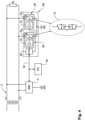
- Fig. 4 shows a modular circuit arrangement 60 with two circuit arrangements 20 according to the invention.
- the circuit arrangement 20 according to the invention is each viewed as a module which simultaneously impresses different fault resistances R f1 , R f2 at different locations, for example on different active conductors L1, L2 of the power supply system 2.
- the first electrical circuit arrangement 20 according to the invention is connected to the active conductor L1
- the second electrical circuit arrangement 20 according to the invention is connected to the conductor L2, each to earth. Both electrical circuit arrangements 20 are controlled by a central control unit 50.
- the central control unit 50 is connected to the insulation monitoring device 4 to be tested via a communication connection 52. Any data, particularly data for signaling, can be exchanged between the modular circuit arrangement 60 and the insulation monitoring device 4 via this communication connection 52.
- the communication connection 52 itself can be wired or wireless and integrated into a common data network with the control device 34.
Landscapes
- Physics & Mathematics (AREA)
- General Physics & Mathematics (AREA)
- Measurement Of Resistance Or Impedance (AREA)
- Control Of Voltage And Current In General (AREA)
Description
- Die Erfindung betrifft eine elektrische Schaltungsanordnung und ein Verfahren zur Funktionsprüfung eines Überwachungsgerätes für ein elektrisches Stromversorgungssystem, mit einem Prüfwiderstand, der zwischen einen aktiven Leiter des Stromversorgungssystems und Erde schaltbar ist und einen einstellbaren Widerstands-Istwert aufweist.
- Des Weiteren betrifft die Erfindung eine modulare Schaltungsanordnung bestehend aus mehreren erfindungsgemäßen elektrischen Schaltungsanordnungen.
- Sicherheitsvorschriften für elektrische Anlagen wie beispielsweise Stromversorgungssysteme und daran angeschlossene Betriebsmittel sowie Anforderungen an Schutzmaßnahmen zur Gewährleistung der elektrischen Sicherheit gewinnen in einer auf der Versorgung mit elektrischer Energie beruhenden Volkswirtschaft zunehmend an Bedeutung. Dabei ist nicht nur die richtige Auswahl geeigneter Überwachungsgeräte, sondern auch deren einwandfreie Funktion entscheidend, um (Isolations-)Fehler frühzeitig zu erkennen und dadurch entstehende Ausfallzeiten der elektrischen Anlage und damit verbundene Kosten zu vermeiden.
- Zur Überwachung eines ungeerdeten Stromversorgungssystems (frz. auch Isolé Terre - IT-Netz) ist daher gemäß der Norm IEC 61557-8 ein Isolationsüberwachungsgerät (IMD) als Überwachungseinrichtung vorgeschrieben. In geerdeten Stromversorgungssystemen erfolgt die Überwachung gemäß der Norm IEC 62020 mittels einer Differenzstrom-Überwachungseinrichtung (RCM).
- Diese Überwachungsgeräte müssen daher mittels Erstinbetriebnahmeprüfung und über die gesamte Einsatzdauer in wiederkehrenden Prüfungen mit festgelegten Prüfintervallen auf eine normgerechte Funktion überprüft werden.
- Messverfahren zur Bestimmung des Isolationswiderstands in ungeerdeten Stromversorgungssystemen beruhen prinzipiell auf der Überlagerung einer in dem Isolationsüberwachungsgerät erzeugten Messspannung, sodass sich ein dem Isolationsfehler (Fehlerwiderstand) proportionaler Messstrom einstellt, der an einem Messwiderstand des Isolationsüberwachungsgerätes einen entsprechenden Spannungsabfall hervorruft. Überschreitet der Spannungsabfall infolge eines abgesunkenen Isolationswiderstands und damit eines höheren Messstroms einen bestimmten Wert, so wird eine Meldung ausgelöst.
- Zur Funktionsprüfung des normgemäßen Isolationsüberwachungsgerätes wird als Fehlerwiderstand ein Prüfwiderstand mit einem definierten Widerstandswert in das von dem Isolationsüberwachungsgerät überwachte Netz zwischen einen oder mehreren aktiven Leiter(n) und Erde eingebracht.
- Die Wirkungsweise eines Differenzstrom-Überwachungsgerätes in geerdeten Stromversorgungssystemen beruht auf der Tatsache, dass im fehlerfreien Betrieb der elektrischen Anlage die vektorielle Summe der Ströme auf allen aktiven Leitern einer Zuleitung gleich Null ist und somit auch kein Magnetfeld in einem die Zuleitung umschließenden magnetisierbaren Ringkern eines Messstromwandlers des Differenzstrom-Überwachungsgerätes existiert. Entsteht aufgrund eines Isolationsfehlers ein Fehlerstrom, der außerhalb der Zuleitung über einen Körper bzw. über Erde abfließt, ergibt sich ein Differenzstrom. Das veränderliche Magnetfeld dieses Differenzstroms induziert in einer Sekundärspule des Messstromwandlers eine Spannung, die ein Alarmsignal auslöst, wenn ein vorgewählter Wert des Differenzstroms überschritten wird.
- Zur Funktionsprüfung des normgemäßen Differenzstrom-Überwachungsgerätes ist als Fehlerwiderstand ein Prüfwiderstand mit definiertem Widerstandswert zu schalten, der einen künstlichen, an dem Ringkern des Differenzstrom-Überwachungsgerätes "vorbeigeführten" Fehlerstrom erzeugt.
- Aus der Patentschrift
EP 3 246 715 B1 sind ein Verfahren und eine Vorrichtung zur Funktionsprüfung eines Isolationsüberwachungsgerätes bekannt, bei dem in sich wiederholenden Prüfzyklen zwei unterschiedliche Isolationswiderstände (Fehlerwiderstände) geschaltet werden und die Reaktion des Isolationsüberwachungsgerätes, also der augenblickliche Betriebszustand, ausgewertet wird. - Von der Firma Gossen Metrawatt ist eine Prüfvorrichtung (Prüfgerät) bekannt (http://www.gmc-instuments.de/media/de/product_manual/profi-test-master-seculifeip-iq-ba_d.pdf), bei dem zur Funktionsprüfung des Isolationsüberwachungsgerätes einphasige Fehler mit diskreten Widerstandswerten und manueller Auslösezeit-Erfassung generiert werden können.
- Weiterhin sind auf dem Markt sogenannte "Fehlerstecker" verfügbar, die einen eingebauten Fehlerwiderstand gegen Erde schalten. Dabei werden bei Serviceeinsätzen große, schwere und je nach Anwendung elektrisch unsichere Widerstandsdekaden zur Fehlererzeugung eingesetzt.
- Sämtliche vorgenannten aus dem Stand der Technik bekannten Lösungen weisen den Nachteil auf, dass nur diskrete Widerstandswerte schaltbar sind. Da aber vor allem hochwertige Isolationsüberwachungsgeräte über eine Vielzahl spezieller Messprofile verfügen, genügt es im Hinblick auf die Gewährleistung der funktionalen Sicherheit nicht, mit nur einem bestimmten Widerstandswert oder einer zeitlichen Abfolge diskreter Widerstandswerte zu messen. Vielmehr sind für einen Funktionstest Widerstandsverläufe von Interesse, welche ein reales Systemverhalten der elektrischen Anlage einschließlich des Auftretens symmetrischer Fehler simulieren können, wobei das Auf- und Abschalten der Fehlerwiderstände (Prüfwiderstände) nicht zu einer unzulässigen Strombelastung der elektrischen Anlage führen darf.
- Aus der Patentschrift
DE 10 2018 125 004 B3 ist eine mittels eines Regelkreises gesteuerte Änderung des Widerstandswertes einer Transistor-Kaskade bekannt. Diese Transistor-Kaskade wirkt nicht als Prüfwiderstand, sondern als Ankoppelimpedanz für ein Isolationsüberwachungsgerät, wobei ein sanftes Auf- und Abschalten der Ankoppelimpedanz zur Vermeidung von Überströmen nicht vorgesehen ist. Weitere Nachteile der verfügbaren Prüfvorrichtungen bestehen darin, dass häufig manuelle Eingriffe zur Aufnahme einer Messgröße, beispielsweise der Auslösezeit, erforderlich sind. - Zudem sind bekannte Prüfvorrichtungen oftmals aufgrund ihrer Baugröße und des hohen Gewichtes für den mobilen Einsatz ungeeignet. Weiterer relevanter Stand der Technik findet sich in
US 3 868 665 A ,DE 10 2014 217370 A1 undEP 1 162 470 A1 . - Der vorliegenden Erfindung liegt somit die Aufgabe zugrunde, eine elektrische Schaltungsanordnung und ein Verfahren zur Funktionsprüfung eines Überwachungsgerätes für ein Stromversorgungssystem, insbesondere eines Isolationsüberwachungsgerätes und eines Differenzstrom-Überwachungsgerätes, zu schaffen. Die erfindungsgemäße technische Lehre soll (technisch) flexibel an die Messumgebung und die Messaufgabe anpassbar sein, wobei die elektrische Schaltungsanordnung auch in Bezug auf Baugröße und Gewicht kostengünstig herstellbar und flexibel (ökonomisch) einsetzbar sein soll.
- Diese Aufgabe wird erfindungsgemäß durch die in Anspruch 1 definierte elektrische Schaltungsanordnung gelöst.
- Die mit der Erfindung verwirklichte erfinderische Idee besteht erstens darin, als Prüfwiderstand eine aus Feldeffekttransistoren bestehende bidirektionale Kaskade anstelle diskreter ohmscher Widerstände zu verwenden, wobei die Feldeffekttransistoren nicht wie technisch üblich als Schalter, sondern als veränderbarer ohmscher Widerstand eingesetzt werden. Die bidirektionale Kaskade besteht aus einer Reihenschaltung von zwei spiegelbildlich angeordneten Feldeffekttransistoren.
- Im Leistungsbetrieb können die Feldeffekttransistoren nicht im linearen Betriebsbereich, sondern nahezu ausschließlich im Sättigungsbereich betrieben werden. Daher wird die Feldeffekttransistor-Kaskade von einem analogen Regelkreis in ein ohmsches Verhalten bei Sättigungsbetrieb gezwungen und arbeitet aufgrund der Bidirektionalität im ersten und dritten Quadranten eines Kennlinienfeldes der Feldeffekttransistor-Kaskade. Damit ist sowohl Gleichspannungs- als auch Wechselspannungsbetrieb möglich.
- Ein zweites Kernelement der Erfindung ist die analoge Regelung mittels eines Regelkreises zur wertkontinuierlichen Einstellung des Widerstandswertes für den Prüfwiderstand. Mit einer gesteuerten Widerstandsänderung wird der Widerstandswert der aus Feldeffekttransistoren bestehenden bidirektionalen Kaskade in einem geschlossenen Wirkungskreis auf einen vorgebbaren Widerstands-Sollwert geregelt. Der Regelkreis steuert die Feldeffekttransistoren in ihrem Kennlinienfeld so an, dass eine ohmsche Widerstandskennlinie entsteht.
- Die erfindungsgemäße Kombination der Feldeffekttransistor-Kaskade und deren analoge Regelung bildet aus schaltungstechnischer Sicht ein wertkontinuierliches Äquivalent zu einer diskret veränderlichen Einstellung des Widerstandswertes.
- Neben dem rein technischen Vorteil der durch die wertkontinuierliche Einstellung des Widerstandswertes ermöglichten Einsatzflexibilität besteht auch ein technisch-wirtschaftlicher Vorteil darin, dass durch die Verwendung von nur zwei Feldeffekttransistoren anstatt vieler einzelner Widerstände die Baugröße und das Gewicht stark minimiert werden und somit der Materialaufwand gesenkt werden kann. Dieser Aspekt kommt insbesondere bei Leistungsanwendungen in Stromversorgungssystemen, wie bei der Einprägung ohmscher Fehlerwiderstände zwischen einem aktiven Leiter und Erdpotenzial, zum Tragen.
- Weiterhin ist in technischer Hinsicht von Vorteil, dass aufgrund der analogen Regelung eine theoretisch unendlich feine Auflösung des einstellbaren Widerstandswertes erreicht werden kann, welcher letztlich nur durch die Auflösung der digitalen Sollwert-Vorgabe bestimmt wird. Die Änderung des Widerstandswertes kann aufgrund der analogen Regelung in vorteilhafterweise sowohl wertkontinuierlich als auch zeitkontinuierlich vollzogen werden, da keine Schaltvorgänge stattfinden. Dies ist bei bekannten diskret geschalteten Widerstandsdekaden nicht ohne weiteres möglich.
- Durch die stufenlose Einstellung der Widerstandswerte wird ein wert- und zeitkontinuierlicher (Fehler-)Widerstandsverlauf zur Prüfung der Überwachungsfunktion ermöglicht, bei dem ein reales Systemverhalten nachgestellt werden kann.
- Erfindungsgemäß weist die Regelung auf: Einen Transformationsblock, welcher mittels eines Ist-Stroms den vorgebbaren Widerstands-Sollwert in eine Soll-Spannung als Führungsgröße transformiert;
- eine Strommessung, welche einen durch die Transistor-Kaskade fließenden Transistor-Strom erfasst und skaliert als den Ist-Strom in den Transformationsblock zurückführt;
- ein Vergleichsglied, welches die Soll-Spannung mit einer Ist-Spannung vergleicht und eine Differenzspannung als Regelabweichung bildet; eine Spannungsmessung, welche eine über der Transistor-Kaskade abfallende Transistor-Spannung erfasst und skaliert als die Ist-Spannung in das Vergleichsglied zurückführt;
- einen Regler, der aus der Differenzspannung eine Stellgröße zur Ansteuerung einer Regelstrecke erzeugt, die durch die Transistor-Kaskade mit dem Widerstandswert als Regelgröße gebildet ist;
- eine steuerbare Schalteinrichtung, welche die Ist-Spannung auf den Wert Null schaltet, um die Regelung herunterzufahren.
- Der als bidirektionale Transistor-Kaskade ausgebildete Prüfwiderstand mit dem veränderlichen Widerstandswert als Regelgröße bildet die Regelstrecke des Regelkreises. Innerhalb der Regelstrecke ist der bidirektionalen Transistor-Kaskade eine Transistor-Treiberschaltung vorgeschaltet, die durch die von dem Regler bereitgestellte Stellgröße angesteuert wird.
- Der Regler wiederum erzeugt die Stellgröße aus der Differenzspannung, die in dem Vergleichsglied erzeugt wird.
- Die Differenzspannung stellt die Regelabweichung zwischen der Soll-Spannung und der Ist-Spannung dar, wobei die Spannungsmessung die über der Transistor-Kaskade abfallende Transistorspannung erfasst und skaliert als Ist-Spannung in das Vergleichsglied zurückführt.
- Die Soll-Spannung wird als Führungsgröße aus einem vorgebbaren Soll-Widerstandswert mittels des Ist-Stroms in dem Transformationsblock ermittelt.
- Durch die Strommessung wird der durch die Transistor-Kaskade fließende Transistorstrom ermittelt und skaliert als Ist-Strom dem Transformationsblock zugeführt.
- Zur Einstellung eines gewünschten Widerstandswertes für den Prüfwiderstand wird der Regelung ein Sollwert des Widerstandswertes vorgegeben. Der gewünschte Widerstandswert stellt sich in dem Regelkreis mittels Rückkopplung der Strommessung des in der Transistor-Kaskade fließenden Transistorstroms und mittels Rückkopplung der Spannungsmessung der über der Transistor-Kaskade abfallenden Transistorspannung ein.
- Da der Prüfwiderstand, also die bidirektionale Transistor-Kaskade, zwischen dem aktiven Leiter und Erde angeschlossen ist, wirkt die Leiter-Erde-Spannung als auf die Regelstrecke einwirkende Störgröße, sodass die Stellgröße zum Einhalten des Widerstands-Sollwertes in einem Wechselspannungs-Stromversorgungssystem fortlaufend nachgeführt werden muss. In einem reinen Gleichspannungs-Stromversorgungssystem mit konstanter Spannung wäre die Stellgröße für einen vorgegebenen Widerstands-Sollwert hingegen konstant.
- Um die Regelung herunterzufahren, also den Widerstandswert gegen Unendlich zu schalten - gleichbedeutend mit einem verschwindenden Stromfluss über die Transistor-Kaskade - wird in der steuerbaren Schalteinrichtung die Ist-Spannung auf den Wert Null geschaltet.
- Ein Abschalten der Regelung erfolgt somit dadurch, dass die Ist-Spannung - der Ausgang der Spannungsmessung - auf das Massepotential gezogen wird. Der PI-Regler (siehe unten) wird die Regelabweichung so lange durch das Herunterfahren der Stellgröße reduzieren, bis diese Regelabweichung konstant null ist.
- Wird für ein erneutes Hochfahren der Regelung die Ist-Spannung durch Schließen der steuerbaren Schalteinrichtung wieder freigegeben, so ist die Regelabweichung aufgrund des fehlenden Ist-Stroms zunächst negativ. Dem folgt der PI-Regler dann mit einem kontinuierlichen Erhöhen der Stellgröße bis die Regelabweichung wieder bei null ist.
- Aufgrund dessen, dass sich die Stellgröße bei dem PI-Regler nicht sprunghaft ändert, kann in vorteilhafterweise von einer sanften Abschaltung und einer sanften Zuschaltung des Prüfwiderstands gesprochen werden. Die Gefahr einer Übersteuerung der Regelstrecke sowie unerwünschte Überströme werden somit verhindert. Durch diesen Regelmechanismus bleibt der Regelkreis in seinem vorgesehenen Regelverhalten und führt zu der sanften Abschaltung und der sanften Zuschaltung.
- Weiterhin weist die elektrische Schaltungsanordnung einen Mikrocontroller zur Vorgabe des Widerstands-Sollwertes über ein digitales Einstellelement und zur Ansteuerung der Schalteinrichtung mittels eines Schaltsignals auf.
- Über den Mikrocontroller wird der Widerstands-Sollwert in digitaler Form vorgegeben und über das digitale Einstellelement als analoges Signal an den Eingang des Transformationsblocks weitergeleitet. Das digitale Einstellelement kann beispielsweise als digitales Potentiometer oder als Digital-Analog-Umsetzer ausgeführt sein.
- Des Weiteren stellt der Mikrocontroller ein Schaltsignal zur Verfügung, welches unmittelbar oder, verknüpft mit weiteren Signalen (Überstrom-Signal, Übertemperatur-Signal), über eine Digitalschaltung der Schalteinrichtung zugeführt wird.
- Mit Vorteil ist der Mikrocontroller dazu konfiguriert, ein amplitudenmoduliertes Widerstandsmuster aus zeitlich aufeinanderfolgenden Widerstands-Sollwerten vorzugeben.
- Der Mikrocontroller kann dafür eingerichtet sein, eine definierte zeitliche Abfolge von unterschiedlichen Widerstands-Sollwerten vorzugeben, welche von dem Überwachungsgerät bei der Erfassung des Fehlerstroms als Signalfolge (Fehlerstromsignatur) erkannt wird, um eine bestimmte Aktion auszulösen. Beispielsweise kann dieses Widerstandsmuster als Startsignal für eine Prüfphase interpretiert werden.
- In vorteilhafterweise weist die elektrische Schaltungsanordnung einen Übertemperatur-Detektor zur Erkennung einer Übertemperatur der Transistor-Kaskade und einen Überstrom-Detektor zur Erkennung eines Überlastwertes des Ist-Stroms auf, wobei ein Übertemperatur-Signal und ein Überstrom-Signal über eine Digitalschaltung mit einem Ausgangssignal des Mikrocontrollers zur Ansteuerung der Schalteinrichtung mittels des Schaltsignals verknüpft sind.
- Die Zuverlässigkeit der erfindungsgemäßen elektrischen Schaltungsanordnung wird somit sichergestellt durch Sicherheitsabschaltungen bei Überstrom und/oder Übertemperatur der Transistor-Kaskade.
- Vorzugsweise ist die Digitalschaltung als RS-Flip-Flop ausgeführt.
- Da unabhängig von dem Schaltsignal des Mikrocontrollers ein Abschalten der Regelung durch die Sicherheitsfunktionen Überstrom- und Übertemperatur-Erkennung ermöglicht werden soll, ist die Digitalschaltung als RS-Flip-Flop ausgeführt. Ein Setzen des RS-Flip-Flops, also das Anschalten der Regelung, kann hierbei nur durch den Mikrocontroller erfolgen. Das Rücksetzen des RS-Flip-Flops, also das Ausschalten der Regelung, kann durch eine Oder-Verknüpfung von Überstrom-Signal, Übertemperatur-Signal und einem Ausgangssignal des Mikrocontrollers erfolgen.
- Vorzugsweise ist der Regler als PI-Regler ausgeführt.
- Als Regler gelangt in der Regelung ein PI-Regler zur Anwendung, der neben seinem proportionalen Verhalten (P-Anteil) einen überlagerten Integralanteil aufweist und damit zu keiner bleibenden Regelabweichung führt.
- Mit Vorteil sind mehrere erfindungsgemäße Schaltungsanordnungen in einer modularen Schaltungsanordnung zusammengefügt, wobei jeder der elektrischen Schaltungsanordnungen ein anderer aktiver Leiter des elektrischen Stromversorgungssystems zugeordnet ist und eine zentrale Steuereinheit zur Steuerung und Überwachung der elektrischen Schaltungsanordnungen implementiert ist.
- Die erfindungsgemäße elektrische Schaltungsanordnung, bestehend aus der Transistor-Kaskade und der Regelung, kann als Modul aufgefasst werden, welches mehrfach dupliziert werden kann, um Fehlerwiderstände (Prüfwiderstände) mit unterschiedlichen Werten zur gleichen Zeit an verschiedenen Stellen des Stromversorgungssystems einprägen zu können.
- Um beispielsweise in einem dreiphasigen Wechselspannungs-Stromversorgungssystem für alle aktiven Leiter Prüfwiderstände gegen Erde schalten zu können, wird die erfindungsgemäße elektrische Schaltungsanordnung demzufolge dreimal benötigt und jeweils mit einem anderen aktiven Leiter verbunden. Diese Möglichkeit deckt damit in idealer Weise auch die Prüfung der normativen Anforderung zur Erkennung symmetrischer Isolationsfehler ab.
- Die modulare Schaltungsanordnung verfügt über eine zentrale Steuereinheit, welche die gewünschten Widerstands-Sollwerte an die Module ausgibt und deren Funktion überwacht.
- Weiterhin ist eine Kommunikationsverbindung zwischen der zentralen Steuereinheit und dem zu prüfenden Überwachungsgerät vorgesehen.
- Über diese Kommunikationsverbindung können Daten in beiden Richtungen zwischen der zentralen Steuereinheit der modularen Schaltungsanordnung und dem Überwachungsgerät ausgetauscht werden, beispielsweise um Meldesignale von dem zu prüfenden Überwachungsgerät zu empfangen oder um eine genaue Auslösezeitmessung zu aktivieren. Andererseits kann über die Kommunikationsverbindung ausgehend von der modularen Schaltungsanordnung dem zu prüfenden Überwachungsgerät beispielsweise mitgeteilt werden, dass eine Prüfung eingeleitet werden soll.
- Die Kommunikationsverbindung kann drahtgebunden oder drahtlos ausgeführt sein.
- Die zuvor beschriebene erfindungsgemäße elektrische Schaltungsanordnung beruht auf einem Verfahren zur Funktionsprüfung eines Überwachungsgerätes für ein elektrisches Stromversorgungssystem, bei dem ein Prüfwiderstand mit einem einstellbaren Widerstandswert zwischen einem aktiven Leiter des Stromversorgungssystems und Erde geschaltet wird. Dabei ist der Prüfwiderstand als bidirektionale Kaskade aus Feldeffekttransistoren ausgeführt und das Einstellen des Widerstandswertes auf einen vorgebbaren Widerstands-Sollwert erfolgt wertkontinuierlich mittels einer analogen Regelung.
- Insoweit treffen auch die vorgenannten für die elektrische Schaltungsanordnung zutreffenden technischen Wirkungen und daraus resultierenden Vorteile auf die Verfahrensmerkmale zu.
- Insbesondere erfolgt ausgehend von einem als bidirektionale Kaskade aus Feldeffekttransistoren ausgeführten Prüfwiderstand das Einstellen des Widerstandswertes auf einem vorgebbaren Widerstands-Sollwert wertkontinuierlich mittels einer analogen Regelung und ermöglicht somit bei minimierter Baugröße und minimiertem Materialaufwand eine flexible Anpassung an die Systemumgebung und an prüftechnische Vorgaben.
- Das Verfahren kann darüber hinaus in Kombination mit einer zentralen Steuereinheit in einer modularen Schaltungsanordnung für ein mehrphasiges Stromversorgungssystem in der Weise angewendet werden, dass mehreren aktiven Leitern jeweils ein angepasster Prüfwiderstand zugeordnet wird. Dabei wird der jeweilige aktive Leiter mit einer erfindungsgemäßen Schaltungsanordnung verbunden und individuell ein Prüfwiderstand mit definiertem Widerstandswert eingestellt.
- Weitere vorteilhafte Ausgestaltungsmerkmale ergeben sich aus der nachfolgenden Beschreibung und den Zeichnungen, die eine bevorzugte Ausführungsform der Erfindung anhand von Beispielen erläutern.
- Es zeigen:
- Fig. 1
- Prüfanordnung mit veränderbaren Prüfwiderständen gemäß dem Stand der Technik zur Funktionsprüfung eines Isolationsüberwachungsgerätes;
- Fig. 2
- ein Kennlinienfeld einer bidirektionalen MOSFET-Transistor-Kaskade;
- Fig. 3
- eine erfindungsgemäße elektrische Schaltungsanordnung mit Transistor-Kaskade und analoger Regelung und
- Fig. 4
- eine modulare Schaltungsanordnung mit zwei erfindungsgemäßen Schaltungsanordnungen.
-
Fig. 1 zeigt eine den Stand der Technik gemäße Prüfanordnung mit veränderbaren Prüfwiderständen zur Funktionsprüfung eines in einem ungeerdeten Stromversorgungssystem 2 installierten Isolationsüberwachungsgerätes 4. - Das Stromversorgungssystem 2 weist zwei aktive Leiter L1, L2 auf, an die ein Verbraucher RL geschaltet ist. Das Isolationsüberwachungsgerät 4 ist zur Isolationswiderstandsmessung (Messung des Fehlerwiderstands in dem Stromversorgungssystem 2) mit den aktiven Leiter L1, L2 und Erde (Erdpotenzial) PE verbunden.
- Zur Erzeugung eines definierten Fehlerwiderstands sind jeweils zwischen einem aktiven Leiter L1, L2 und Erde PE veränderbare Prüfwiderstände Rf1, Rf2 angeordnet, über die jeweils die Leiter-Erde-Spannung UL1-PE, UL2-PE abfällt. Für die Funktionsprüfung des Isolationsüberwachungsgerätes 4 wird ein geschlossener Messkreis über jeweils einen aktiven Leiter L1, L2, die Prüfwiderstände Rf1, Rf2 und Erde PE zurück zu dem Isolationsüberwachungsgerät 4 ausgebildet, in dem ein Fehlerstrom (Messstrom) fließt, der in dem Isolationsüberwachungsgerät 4 ausgewertet werden kann.
- In
Fig. 2 ist ein Kennlinienfeld der bidirektionalen MOSFET-Transistor-Kaskade dargestellt. - Vorzugsweise werden als Transistoren MOSFETs verwendet. In Abhängigkeit der Steuerspannung UGS stellt sich bei über der Transistor-Kaskade angelegten Spannung UDD ein bestimmter über die Kaskade fließender Strom IDD ein.
- Die bidirektionale Transistor-Kaskade 12 besteht aus einer Reihenschaltung von zwei spiegelbildlich angeordneten MOSFET-Transistoren, sodass sich Arbeitsbereiche der Transistor-Kaskade 12 in dem ersten und dritten Quadranten des Kennlinienfeldes ergeben. Durch die analoge Regelung 10 (
Fig. 3 ) wird die Transistor-Kaskade 12 in ein ohmsches Verhalten gezwungen. -
Fig. 3 zeigt die erfindungsgemäße elektrische Schaltungsanordnung 20 mit bidirektionaler Transistor-Kaskade 12 und Regelung 10. - Als Eingangsgröße der Regelung 10 wird zunächst der gewünschte Widerstands-Sollwert R0 vorgegeben, welcher über den Transformationsblock 22 in die Sollspannung U0 transformiert wird. Die Transformation erfolgt über die Strommessung 25, die den über die Transistor-Kaskade 12 fließenden Transistorstrom Im (entspricht IDD in
Fig. 2 ) erfasst und skaliert (k2) als Ist-Strom Ix dem Transformationsblock 22 zuführt. - In dem Vergleichsglied 24 wird aus der Sollspannung U0 und der Ist-Spannung Ux, welche über die Spannungsmessung 26 aus der über der Transistor-Kaskade 12 abfallenden Transistorspannung Um gewonnen und skaliert (k1) wird, eine Differenzspannung Ud gebildet. Die Differenzspannung Ud wird dem Regler 40 - der vorzugsweise ein PI-Regler ist - zugeführt, der daraus eine Stellgröße W zur Ansteuerung der Transistor-Kaskade 12 bildet.
- Die Transistor-Kaskade 12 umfasst neben einer eigentlichen Transistorstrecke 14 eine Treiberschaltung 16 zur Ansteuerung der Transistorstrecke 14.
- Die Regelung 10 bewirkt, dass sich der Widerstands-Istwert Rx der Transistorstrecke 14 der Transistor-Kaskade 12 auf den vorgegebenen Widerstands-Sollwert R0 einstellt.
- Um die Regelung 10 ein- und ausschalten zu können, insbesondere aber um ein sanftes Herunterfahren und Anlaufen zu bewirken, ist zwischen der Spannungsmessung 26 und dem Vergleichsglied 24 eine Schalteinrichtung 27 vorgesehen, welche die Ist-Spannung Ux auf den Wert Null (Massepotential) zieht.
- Die Schalteinrichtung 27 kann direkt mittels eines Schaltsignals Su von dem Mikrocontroller 30 oder über die Digitalschaltung 44 angesteuert werden.
- Die als RS-Flip-Flop ausgeführte Digitalschaltung 44 ist dann vorzusehen, wenn mittels eines Übertemperatur-Detektors 42 eine Ist-Temperatur Tx der Transistor-Kaskade 12 und/oder mittels eines Überstrom-Detektors 43 ein unzulässig hoher Wert des Ist-Stroms Ix festgestellt wird und an dem Ausgang des Übertemperatur-Detektors 42 und/oder des Überstrom-Detektors 43 ein Übertemperatur-Signal St und/oder ein Überstromsignal Si ausgegeben wird. Das Übertemperatur-Signal St und das Überstrom-Signal Si werden über das RS-Flip-Flop 44 mit einem Ausgangssignal Sa des Mikrocontrollers 30 zu dem Schaltsignal Su verknüpft, welches die Schalteinrichtung 27 steuert.
- Der Mikrocontroller 30 gibt über ein digitales Einstellelement 32 den Widerstands-Sollwert R0 als Führungsgröße vor.
- Zur übergeordneten Steuerung kann der Mikrocontroller 30 mit einem Steuergerät 34 wie beispielsweise einem PC, Laptop, Smartphone oder einer speicherprogrammierbaren Steuerung (SPS) verbunden werden.
-
Fig. 4 zeigt eine modulare Schaltungsanordnung 60 mit zwei erfindungsgemäßen Schaltungsanordnungen 20. - Die erfindungsgemäße Schaltungsanordnung 20 wird dabei jeweils als ein Modul aufgefasst, welches gleichzeitig unterschiedliche Fehlerwiderstände Rf1, Rf2 an unterschiedlichen Stellen, beispielsweise an verschiedenen aktiven Leitern L1, L2 des Stromversorgungssystems 2 einprägt.
- Vorliegend ist die erste erfindungsgemäße elektrische Schaltungsanordnung 20 an den aktiven Leiter L1, die zweite erfindungsgemäße elektrische Schaltungsanordnung 20 an den Leiter L2 jeweils gegen Erde angeschlossen. Beide elektrischen Schaltungsanordnungen 20 werden von einer zentralen Steuereinheit 50 gesteuert.
- Die zentrale Steuereinheit 50 ist über eine Kommunikationsverbindung 52 mit dem zu prüfenden Isolationsüberwachungsgerät 4 verbunden. Über diese Kommunikationsverbindung 52 können beliebige Daten insbesondere aber Daten zur Signalisierung zwischen der modularen Schaltungsanordnung 60 und dem Isolationsüberwachungsgerät 4 ausgetauscht werden.
- Die Kommunikationsverbindung 52 selbst kann drahtgebunden oder drahtlos ausgeführt und in ein gemeinsames Datennetzwerk mit dem Steuergerät 34 eingebunden sein.
Claims (15)
- Elektrische Schaltungsanordnung (20) zur Funktionsprüfung eines Überwachungsgerätes (4) für ein Stromversorgungssystem (2), mit einem Prüfwiderstand (Rf1, Rf2), der zwischen einen aktiven Leiter L1, L2) des Stromversorgungssystems (2) und Erde (PE) schaltbar ist und einen einstellbaren Widerstands-Istwert (Rx) aufweist,mit einer bidirektionalen Kaskade (12) mit Feldeffekttransistoren als Prüfwiderstand (Rf1, Rf2) und einer analogen Regelung (10) zur wertkontinuierlichen Einstellung des Widerstands-Istwertes (Rx) auf einen vorgebbaren Widerstands-Sollwert (R0), wobei die Regelung aufweisteinen Transformationsblock (22), welcher mittels eines Ist-Stroms (Ix) den vorgebbaren Widerstands-Sollwert (R0) in eine Soll-Spannung (U0) als Führungsgröße transformiert;eine Strommessung (25), welche einen durch die Transistor-Kaskade (12) fließenden Transistor-Strom (Im) erfasst und skaliert als den Ist-Strom (Ix) in den Transformationsblock (22) zurückführt;ein Vergleichsglied (24), welches die Soll-Spannung (U0) mit einer Ist-Spannung (Ux) vergleicht und eine Differenzspannung (Ud) als Regelabweichung bildet;eine Spannungsmessung (26), welche eine über der Transistor-Kaskade (12) abfallende Transistor-Spannung (Um) erfasst und skaliert als die Ist-Spannung (Ux) in das Vergleichsglied (24) zurückführt;einen Regler (40), der aus der Differenzspannung (Ud) eine Stellgrö-ße (W) zur Ansteuerung einer Regelstrecke erzeugt, die durch die Transistor-Kaskade (12) mit dem Widerstandswert als Regelgröße (Rx) gebildet ist;gekennzeichnet durcheine steuerbare Schalteinrichtung (27), welche die Ist-Spannung (Ux) auf den Wert Null schaltet, um die Regelung (10) herunterzufahren und ein sanftes Abschalten und Zuschalten des Prüfwiderstands (Rf1, Rf2) zu bewirken.
- Elektrische Schaltungsanordnung (20) nach Anspruch 1,
gekennzeichnet durch
einen Mikrocontroller (30) zur Vorgabe des Widerstands-Sollwertes (R0) über ein digitales Einstellelement (32) und zur Ansteuerung der Schalteinrichtung (27) mittels eines Schaltsignals (Su). - Elektrische Schaltungsanordnung (20) nach Anspruch 2,
dadurch gekennzeichnet,
dass der Mikrocontroller (30) dazu konfiguriert ist, ein amplitudenmoduliertes Widerstandsmuster aus zeitlich aufeinanderfolgenden Widerstands-Sollwerten (R0) vorzugeben. - Elektrische Schaltungsanordnung (20) nach Anspruch 2 oder 3,
dadurch gekennzeichnet,
dass die Regelung (10) einen Übertemperatur-Detektor (42) zur Erkennung einer Übertemperatur der Transistor-Kaskade (12) und einen Überstrom-Detektor (43) zur Erkennung eines Überlastwertes des Ist-Stroms (Ix) aufweist, wobei ein Übertemperatur-Signal (St) und ein Überstrom-Signal (Si) über eine Digitalschaltung (44) mit einem Ausgangssignal (Sa) des Mikrocontrollers (30) zur Ansteuerung der Schalteinrichtung (27) verknüpft sind. - Elektrische Schaltungsanordnung (20) nach Anspruch 4,
dadurch gekennzeichnet,
dass die Digitalschaltung (44) als RS-Flip-Flop ausgeführt ist. - Elektrische Schaltungsanordnung (20) nach einem der Ansprüche 1 bis 5,
dadurch gekennzeichnet,
dass der Regler (40) als PI-Regler ausgeführt ist. - Modulare Schaltungsanordnung (60) bestehend aus mehreren elektrischen Schaltungsanordnungen (20) nach einem der Ansprüche 1 bis 6,
dadurch gekennzeichnet,
dass jeder der elektrischen Schaltungsanordnungen (20) ein anderer aktiver Leiter (L1, L2) des elektrischen Stromversorgungssystems (2) zugeordnet ist und eine zentrale Steuereinheit (50) zur Steuerung und Überwachung der elektrischen Schaltungsanordnungen (20) implementiert ist. - Modulare Schaltungsanordnung (60) nach Anspruch 7,
gekennzeichnet durch
eine Kommunikationsverbindung (52) zwischen der zentralen Steuereinheit (50) und dem Überwachungsgerät (4). - Verfahren zur Funktionsprüfung eines Überwachungsgerätes (4) für ein elektrisches Stromversorgungssystem (2), umfassend die VerfahrensschritteSchalten eines Prüfwiderstands (Rf1, Rf2) mit einem einstellbaren Widerstands-Istwert (Rx) zwischen einen aktiven Leiter (L1, L2) des Stromversorgungssystems (2) und Erde (PE),dadurch gekennzeichnet, dassder Prüfwiderstand (Rf1, Rf2) eine bidirektionale Kaskade (12) aus Feldeffekttransistoren ist und das Einstellen des Widerstands-Istwertes (Rx) auf einen vorgebbaren Widerstands-Sollwert (R0) wertkontinuierlich mittels einer analogen Regelung (10) erfolgt.
- Verfahren nach Anspruch 9,
dadurch gekennzeichnet,
dass durch die Regelung (10)in einem Transformationsblock (22) mittels eines Ist-Stroms (Ix) der vorgebbare Widerstands-Sollwert (R0) in eine Soll-Spannung (U0) als Führungsgröße transformiert wird;mit einer Strommessung (25) ein durch die Transistor-Kaskade (12) fließenden Transistor-Strom (Im) erfasst und skaliert als der Ist-Strom (Ix) in den Transformationsblock (22) zurückgeführt wird; in einem Vergleichsglied (24) die Soll-Spannung (U0) mit einer Ist-Spannung (Ux) verglichen und eine Differenzspannung (Ud) als Regelabweichung gebildet wird;mit einer Spannungsmessung (26) eine über der Transistor-Kaskade (12) abfallende Transistor-Spannung (Um) erfasst und skaliert als die Ist-Spannung (Ux) in das Vergleichsglied (24) zurückgeführt wird; mittels eines Reglers (40) aus der Differenzspannung (Ud) eine Stellgröße (W) zur Ansteuerung einer Regelstrecke erzeugt wird, wobei die Regelstrecke durch die Transistor-Kaskade (12) mit dem Widerstands-Istwert (Rx) als Regelgröße gebildet wird undmit einer steuerbaren Schalteinrichtung (27) die Ist-Spannung (Ux) auf den Wert Null geschaltet wird, um die Regelung (10) herunterzufahren. - Verfahren nach Anspruch 10,
dadurch gekennzeichnet,
dass ein Mikrocontroller (30) den Widerstands-Sollwert (R0) über ein digitales Einstellelement (32) vorgibt und mittels eines Schaltsignals die Schalteinrichtung (27) ansteuert. - Verfahren nach Anspruch 11,
dadurch gekennzeichnet,
dass der Mikrocontroller (30) ein amplitudenmoduliertes Widerstandsmuster aus zeitlich aufeinanderfolgenden Widerstands-Sollwerten (R0) vorgibt. - Verfahren nach Anspruch 11 oder 12,
gekennzeichnet durchErkennen einer Übertemperatur der Transistor-Kaskade in der Regelung (10) mittels eines Übertemperatur-Detektors (42);Erkennen eines Überlastwertes des Ist-Stroms (Ix) mittels eines Überstrom-Detektors (43), wobei ein Übertemperatur-Signal (St) und ein Überstrom-Signal (Si) über eine Digitalschaltung (44) mit einem Ausgangssignal (Sa) des Mikrocontrollers (30) zur Ansteuerung der Schalteinrichtung (27) verknüpft werden. - Verfahren nach Anspruch 13,
dadurch gekennzeichnet,
dass die Digitalschaltung (44) als RS-Flip-Flop implementiert wird. - Verfahren nach einem der Ansprüche 10 bis 14,
dadurch gekennzeichnet,
dass der Regler (40) eine PI-Regelung ausführt.
Applications Claiming Priority (1)
| Application Number | Priority Date | Filing Date | Title |
|---|---|---|---|
| DE102020111807.4A DE102020111807B9 (de) | 2020-04-30 | 2020-04-30 | Elektrische Schaltungsanordnung und Verfahren zur Funktionsprüfung eines Überwachungsgeräts für ein elektrisches Stromversorgungssystem |
Publications (2)
| Publication Number | Publication Date |
|---|---|
| EP3904896A1 EP3904896A1 (de) | 2021-11-03 |
| EP3904896B1 true EP3904896B1 (de) | 2024-03-13 |
Family
ID=75588102
Family Applications (1)
| Application Number | Title | Priority Date | Filing Date |
|---|---|---|---|
| EP21169290.0A Active EP3904896B1 (de) | 2020-04-30 | 2021-04-20 | Elektrische schaltungsanordnung und verfahren zur funktionsprüfung eines überwachungsgeräts für ein elektrisches stromversorgungssystem |
Country Status (4)
| Country | Link |
|---|---|
| US (1) | US11486937B2 (de) |
| EP (1) | EP3904896B1 (de) |
| CN (1) | CN113589060A (de) |
| DE (1) | DE102020111807B9 (de) |
Families Citing this family (3)
| Publication number | Priority date | Publication date | Assignee | Title |
|---|---|---|---|---|
| DE102021006389B3 (de) * | 2021-12-28 | 2023-06-29 | Bender Gmbh & Co. Kg | Verfahren zur automatischen Erstellung von anlagenspezifischen Messprofilen für ein Isolationsüberwachungssystem |
| DE102024108470A1 (de) * | 2024-03-25 | 2025-09-25 | Bender Gmbh & Co. Kg | Anordnung und Verfahren zur Simulation eines ungeerdeten Stromversorgungssystems |
| CN118426447B (zh) * | 2024-05-28 | 2024-10-29 | 苏州智行众维智能科技有限公司 | 一种基于整车硬件在环测试的多范围电阻模拟板卡 |
Family Cites Families (13)
| Publication number | Priority date | Publication date | Assignee | Title |
|---|---|---|---|---|
| US3868665A (en) * | 1974-02-08 | 1975-02-25 | Midland Ross Corp | Ground fault current detector |
| DE3513848A1 (de) * | 1985-04-17 | 1986-10-23 | Quante Fernmeldetechnik GmbH, 5600 Wuppertal | Schaltung zur ueberwachung der isolationswiderstaende einer schar von baugruppen einer elektrischen anlage mit gemeinsamer erdfreier stromversorgung, insbesondere einer fernmelde- oder signaltechnischen einrichtung |
| FR2810115B1 (fr) * | 2000-06-09 | 2003-05-30 | Florent Raymond Andre Mengin | Appareil de test des controleurs d'isolement de reseaux electriques |
| JP5262945B2 (ja) * | 2009-04-15 | 2013-08-14 | 株式会社デンソー | 電子装置 |
| CN101534118B (zh) * | 2009-04-16 | 2010-12-01 | 浙江大学 | 一种受控等效电阻模块 |
| AT510501A3 (de) * | 2010-09-28 | 2017-02-15 | Eaton Gmbh | Fehlerstromschutzschalter |
| US9128119B2 (en) | 2013-03-29 | 2015-09-08 | Hamilton Sundstrand Corporation | Electrical circuit testing |
| DE102014217370A1 (de) * | 2013-08-31 | 2015-03-05 | Ford Global Technologies, Llc | Isolationsprüfung von fahrzeughoch-/niederspannungssystemen |
| DE102014103910A1 (de) * | 2014-03-21 | 2015-09-24 | Schlüter-Systems Kg | Widerstandsmessgerät |
| WO2016105551A1 (en) * | 2014-12-25 | 2016-06-30 | Tomimbang Wendell E | Apparatus, system and method for total protection from electrical faults |
| US9966943B2 (en) * | 2016-03-31 | 2018-05-08 | Infineon Technologies Ag | System and method for a high-side power switch |
| DE102016207197B3 (de) | 2016-04-27 | 2017-07-13 | Bender Gmbh & Co. Kg | Verfahren und Vorrichtungen zur Funktionsprüfung eines Isolationsüberwachungsgerätes |
| DE102018125004B3 (de) | 2018-10-10 | 2019-12-12 | Bender Gmbh & Co. Kg | Elektrische Schaltungsanordnung und Verfahren zur Ankopplung eines Isolationsüberwachungsgerätes an ein ungeerdetes Stromversorgungssystem |
-
2020
- 2020-04-30 DE DE102020111807.4A patent/DE102020111807B9/de not_active Expired - Fee Related
-
2021
- 2021-04-20 EP EP21169290.0A patent/EP3904896B1/de active Active
- 2021-04-29 CN CN202110477000.0A patent/CN113589060A/zh active Pending
- 2021-04-29 US US17/243,672 patent/US11486937B2/en active Active
Also Published As
| Publication number | Publication date |
|---|---|
| US20210341542A1 (en) | 2021-11-04 |
| DE102020111807A9 (de) | 2022-12-08 |
| US11486937B2 (en) | 2022-11-01 |
| DE102020111807B9 (de) | 2023-04-13 |
| EP3904896A1 (de) | 2021-11-03 |
| DE102020111807B4 (de) | 2022-11-03 |
| DE102020111807A1 (de) | 2021-11-04 |
| CN113589060A (zh) | 2021-11-02 |
Similar Documents
| Publication | Publication Date | Title |
|---|---|---|
| DE102020111807B9 (de) | Elektrische Schaltungsanordnung und Verfahren zur Funktionsprüfung eines Überwachungsgeräts für ein elektrisches Stromversorgungssystem | |
| DE102012208111B3 (de) | Pulsgenerator-Schaltungsanordnung und Verfahren zur Erzeugung von Pulssignalen für die Isolationsfehlersuche in IT-Netzen | |
| DE102013207141A1 (de) | Allstromsensitive Fehlerstrom-Schutzeinrichtung (RCD) mit Parameterkonfiguration | |
| DE102013101050A1 (de) | Sicherheitsschaltvorrichtung mit sicherem Netzteil | |
| EP3311503B1 (de) | Feldgerät-koppeleinrichtung und system | |
| EP1754069A1 (de) | Stromsensor | |
| EP3641087A1 (de) | Elektrische schaltungsanordnung und verfahren zur ankopplung eines isolationsüberwachungsgerätes an ein ungeerdetes stromversorgungssystem | |
| EP2559127B1 (de) | Fehlerstromschutzschalter | |
| WO2010049185A1 (de) | Anordnung und verfahren zur phasenanschnitt-steuerung | |
| WO2014060184A1 (de) | Ansteuerschaltung für mindestens zwei schütze und ein verfahren zum betrieb mindestens zweier schütze | |
| DE112004002396T5 (de) | Erweiterter unverzögerter Schutz | |
| EP1845548B1 (de) | Einrichtung, Schaltungsanordnung und Verfahren zur Isolations- und Erdschlussüberwachung in einem IT-System | |
| DE3516251A1 (de) | Vorrichtung zum ueberwachen eines schalters oder eines widerstandskreises | |
| DE68908342T2 (de) | Elektrotherapie-Gerät. | |
| EP3893006A1 (de) | Elektrische schaltungsanordnung und verfahren zur galvanisch getrennten, allstromsensitiven differenzstrom-messung mit hoher auflösung | |
| EP3652860B1 (de) | Pegelwandler und ein verfahren zum wandeln von pegelwerten in fahrzeugsteuergeräten | |
| EP2876509B1 (de) | Sicherheitssteuerung | |
| EP1058430B1 (de) | Flankensteuervorrichtung für ein elektrisches Datenübertragungssystem | |
| DE102012007667A1 (de) | Messverfahren des Widerstandes einer passiven Last,welche einen linearen Zweipol mit in Reihe geschalteten Dioden aufweist | |
| WO2017140547A1 (de) | Prüfgerät und verfahren zum prüfen einer steuereinheit einer schaltvorrichtung einer schaltanlage | |
| EP2737514B1 (de) | Schaltgeraet | |
| AT526991B1 (de) | Überwachte Stromversorgungseinheit, insbesondere zur Speisung von Komponenten eines Brand- oder Gefahrenmeldesystems | |
| DE10057375C1 (de) | Temperaturüberwachungsschaltung für pulsweitenmoduliert betriebene, geregelte induktive Verbraucher | |
| WO2024009230A1 (de) | Verfahren und schaltung zur stromkontrolle | |
| EP4624944A1 (de) | Anordnung und verfahren zur simulation eines ungeerdeten stromversorgungssystems |
Legal Events
| Date | Code | Title | Description |
|---|---|---|---|
| PUAI | Public reference made under article 153(3) epc to a published international application that has entered the european phase |
Free format text: ORIGINAL CODE: 0009012 |
|
| STAA | Information on the status of an ep patent application or granted ep patent |
Free format text: STATUS: THE APPLICATION HAS BEEN PUBLISHED |
|
| AK | Designated contracting states |
Kind code of ref document: A1 Designated state(s): AL AT BE BG CH CY CZ DE DK EE ES FI FR GB GR HR HU IE IS IT LI LT LU LV MC MK MT NL NO PL PT RO RS SE SI SK SM TR |
|
| B565 | Issuance of search results under rule 164(2) epc |
Effective date: 20210920 |
|
| STAA | Information on the status of an ep patent application or granted ep patent |
Free format text: STATUS: REQUEST FOR EXAMINATION WAS MADE |
|
| 17P | Request for examination filed |
Effective date: 20220405 |
|
| RBV | Designated contracting states (corrected) |
Designated state(s): AL AT BE BG CH CY CZ DE DK EE ES FI FR GB GR HR HU IE IS IT LI LT LU LV MC MK MT NL NO PL PT RO RS SE SI SK SM TR |
|
| GRAP | Despatch of communication of intention to grant a patent |
Free format text: ORIGINAL CODE: EPIDOSNIGR1 |
|
| STAA | Information on the status of an ep patent application or granted ep patent |
Free format text: STATUS: GRANT OF PATENT IS INTENDED |
|
| INTG | Intention to grant announced |
Effective date: 20231006 |
|
| GRAS | Grant fee paid |
Free format text: ORIGINAL CODE: EPIDOSNIGR3 |
|
| GRAA | (expected) grant |
Free format text: ORIGINAL CODE: 0009210 |
|
| STAA | Information on the status of an ep patent application or granted ep patent |
Free format text: STATUS: THE PATENT HAS BEEN GRANTED |
|
| AK | Designated contracting states |
Kind code of ref document: B1 Designated state(s): AL AT BE BG CH CY CZ DE DK EE ES FI FR GB GR HR HU IE IS IT LI LT LU LV MC MK MT NL NO PL PT RO RS SE SI SK SM TR |
|
| REG | Reference to a national code |
Ref country code: GB Ref legal event code: FG4D Free format text: NOT ENGLISH |
|
| REG | Reference to a national code |
Ref country code: CH Ref legal event code: EP |
|
| REG | Reference to a national code |
Ref country code: DE Ref legal event code: R096 Ref document number: 502021002940 Country of ref document: DE |
|
| REG | Reference to a national code |
Ref country code: IE Ref legal event code: FG4D Free format text: LANGUAGE OF EP DOCUMENT: GERMAN |
|
| PG25 | Lapsed in a contracting state [announced via postgrant information from national office to epo] |
Ref country code: LT Free format text: LAPSE BECAUSE OF FAILURE TO SUBMIT A TRANSLATION OF THE DESCRIPTION OR TO PAY THE FEE WITHIN THE PRESCRIBED TIME-LIMIT Effective date: 20240313 |
|
| REG | Reference to a national code |
Ref country code: LT Ref legal event code: MG9D |
|
| PG25 | Lapsed in a contracting state [announced via postgrant information from national office to epo] |
Ref country code: GR Free format text: LAPSE BECAUSE OF FAILURE TO SUBMIT A TRANSLATION OF THE DESCRIPTION OR TO PAY THE FEE WITHIN THE PRESCRIBED TIME-LIMIT Effective date: 20240614 |
|
| REG | Reference to a national code |
Ref country code: NL Ref legal event code: MP Effective date: 20240313 |
|
| PG25 | Lapsed in a contracting state [announced via postgrant information from national office to epo] |
Ref country code: RS Free format text: LAPSE BECAUSE OF FAILURE TO SUBMIT A TRANSLATION OF THE DESCRIPTION OR TO PAY THE FEE WITHIN THE PRESCRIBED TIME-LIMIT Effective date: 20240613 Ref country code: HR Free format text: LAPSE BECAUSE OF FAILURE TO SUBMIT A TRANSLATION OF THE DESCRIPTION OR TO PAY THE FEE WITHIN THE PRESCRIBED TIME-LIMIT Effective date: 20240313 |
|
| PG25 | Lapsed in a contracting state [announced via postgrant information from national office to epo] |
Ref country code: ES Free format text: LAPSE BECAUSE OF FAILURE TO SUBMIT A TRANSLATION OF THE DESCRIPTION OR TO PAY THE FEE WITHIN THE PRESCRIBED TIME-LIMIT Effective date: 20240313 |
|
| PG25 | Lapsed in a contracting state [announced via postgrant information from national office to epo] |
Ref country code: RS Free format text: LAPSE BECAUSE OF FAILURE TO SUBMIT A TRANSLATION OF THE DESCRIPTION OR TO PAY THE FEE WITHIN THE PRESCRIBED TIME-LIMIT Effective date: 20240613 Ref country code: NO Free format text: LAPSE BECAUSE OF FAILURE TO SUBMIT A TRANSLATION OF THE DESCRIPTION OR TO PAY THE FEE WITHIN THE PRESCRIBED TIME-LIMIT Effective date: 20240613 Ref country code: LT Free format text: LAPSE BECAUSE OF FAILURE TO SUBMIT A TRANSLATION OF THE DESCRIPTION OR TO PAY THE FEE WITHIN THE PRESCRIBED TIME-LIMIT Effective date: 20240313 Ref country code: HR Free format text: LAPSE BECAUSE OF FAILURE TO SUBMIT A TRANSLATION OF THE DESCRIPTION OR TO PAY THE FEE WITHIN THE PRESCRIBED TIME-LIMIT Effective date: 20240313 Ref country code: GR Free format text: LAPSE BECAUSE OF FAILURE TO SUBMIT A TRANSLATION OF THE DESCRIPTION OR TO PAY THE FEE WITHIN THE PRESCRIBED TIME-LIMIT Effective date: 20240614 Ref country code: FI Free format text: LAPSE BECAUSE OF FAILURE TO SUBMIT A TRANSLATION OF THE DESCRIPTION OR TO PAY THE FEE WITHIN THE PRESCRIBED TIME-LIMIT Effective date: 20240313 Ref country code: ES Free format text: LAPSE BECAUSE OF FAILURE TO SUBMIT A TRANSLATION OF THE DESCRIPTION OR TO PAY THE FEE WITHIN THE PRESCRIBED TIME-LIMIT Effective date: 20240313 Ref country code: BG Free format text: LAPSE BECAUSE OF FAILURE TO SUBMIT A TRANSLATION OF THE DESCRIPTION OR TO PAY THE FEE WITHIN THE PRESCRIBED TIME-LIMIT Effective date: 20240313 |
|
| P01 | Opt-out of the competence of the unified patent court (upc) registered |
Free format text: CASE NUMBER: APP_40111/2024 Effective date: 20240705 |
|
| PG25 | Lapsed in a contracting state [announced via postgrant information from national office to epo] |
Ref country code: SE Free format text: LAPSE BECAUSE OF FAILURE TO SUBMIT A TRANSLATION OF THE DESCRIPTION OR TO PAY THE FEE WITHIN THE PRESCRIBED TIME-LIMIT Effective date: 20240313 Ref country code: LV Free format text: LAPSE BECAUSE OF FAILURE TO SUBMIT A TRANSLATION OF THE DESCRIPTION OR TO PAY THE FEE WITHIN THE PRESCRIBED TIME-LIMIT Effective date: 20240313 |
|
| PG25 | Lapsed in a contracting state [announced via postgrant information from national office to epo] |
Ref country code: NL Free format text: LAPSE BECAUSE OF FAILURE TO SUBMIT A TRANSLATION OF THE DESCRIPTION OR TO PAY THE FEE WITHIN THE PRESCRIBED TIME-LIMIT Effective date: 20240313 |
|
| PG25 | Lapsed in a contracting state [announced via postgrant information from national office to epo] |
Ref country code: NL Free format text: LAPSE BECAUSE OF FAILURE TO SUBMIT A TRANSLATION OF THE DESCRIPTION OR TO PAY THE FEE WITHIN THE PRESCRIBED TIME-LIMIT Effective date: 20240313 |
|
| PG25 | Lapsed in a contracting state [announced via postgrant information from national office to epo] |
Ref country code: IS Free format text: LAPSE BECAUSE OF FAILURE TO SUBMIT A TRANSLATION OF THE DESCRIPTION OR TO PAY THE FEE WITHIN THE PRESCRIBED TIME-LIMIT Effective date: 20240713 |
|
| PG25 | Lapsed in a contracting state [announced via postgrant information from national office to epo] |
Ref country code: SM Free format text: LAPSE BECAUSE OF FAILURE TO SUBMIT A TRANSLATION OF THE DESCRIPTION OR TO PAY THE FEE WITHIN THE PRESCRIBED TIME-LIMIT Effective date: 20240313 Ref country code: PT Free format text: LAPSE BECAUSE OF FAILURE TO SUBMIT A TRANSLATION OF THE DESCRIPTION OR TO PAY THE FEE WITHIN THE PRESCRIBED TIME-LIMIT Effective date: 20240715 |
|
| PG25 | Lapsed in a contracting state [announced via postgrant information from national office to epo] |
Ref country code: EE Free format text: LAPSE BECAUSE OF FAILURE TO SUBMIT A TRANSLATION OF THE DESCRIPTION OR TO PAY THE FEE WITHIN THE PRESCRIBED TIME-LIMIT Effective date: 20240313 Ref country code: CZ Free format text: LAPSE BECAUSE OF FAILURE TO SUBMIT A TRANSLATION OF THE DESCRIPTION OR TO PAY THE FEE WITHIN THE PRESCRIBED TIME-LIMIT Effective date: 20240313 |
|
| PG25 | Lapsed in a contracting state [announced via postgrant information from national office to epo] |
Ref country code: PL Free format text: LAPSE BECAUSE OF FAILURE TO SUBMIT A TRANSLATION OF THE DESCRIPTION OR TO PAY THE FEE WITHIN THE PRESCRIBED TIME-LIMIT Effective date: 20240313 |
|
| PG25 | Lapsed in a contracting state [announced via postgrant information from national office to epo] |
Ref country code: SK Free format text: LAPSE BECAUSE OF FAILURE TO SUBMIT A TRANSLATION OF THE DESCRIPTION OR TO PAY THE FEE WITHIN THE PRESCRIBED TIME-LIMIT Effective date: 20240313 |
|
| PG25 | Lapsed in a contracting state [announced via postgrant information from national office to epo] |
Ref country code: SM Free format text: LAPSE BECAUSE OF FAILURE TO SUBMIT A TRANSLATION OF THE DESCRIPTION OR TO PAY THE FEE WITHIN THE PRESCRIBED TIME-LIMIT Effective date: 20240313 Ref country code: SK Free format text: LAPSE BECAUSE OF FAILURE TO SUBMIT A TRANSLATION OF THE DESCRIPTION OR TO PAY THE FEE WITHIN THE PRESCRIBED TIME-LIMIT Effective date: 20240313 Ref country code: RO Free format text: LAPSE BECAUSE OF FAILURE TO SUBMIT A TRANSLATION OF THE DESCRIPTION OR TO PAY THE FEE WITHIN THE PRESCRIBED TIME-LIMIT Effective date: 20240313 Ref country code: PT Free format text: LAPSE BECAUSE OF FAILURE TO SUBMIT A TRANSLATION OF THE DESCRIPTION OR TO PAY THE FEE WITHIN THE PRESCRIBED TIME-LIMIT Effective date: 20240715 Ref country code: PL Free format text: LAPSE BECAUSE OF FAILURE TO SUBMIT A TRANSLATION OF THE DESCRIPTION OR TO PAY THE FEE WITHIN THE PRESCRIBED TIME-LIMIT Effective date: 20240313 Ref country code: IS Free format text: LAPSE BECAUSE OF FAILURE TO SUBMIT A TRANSLATION OF THE DESCRIPTION OR TO PAY THE FEE WITHIN THE PRESCRIBED TIME-LIMIT Effective date: 20240713 Ref country code: EE Free format text: LAPSE BECAUSE OF FAILURE TO SUBMIT A TRANSLATION OF THE DESCRIPTION OR TO PAY THE FEE WITHIN THE PRESCRIBED TIME-LIMIT Effective date: 20240313 Ref country code: CZ Free format text: LAPSE BECAUSE OF FAILURE TO SUBMIT A TRANSLATION OF THE DESCRIPTION OR TO PAY THE FEE WITHIN THE PRESCRIBED TIME-LIMIT Effective date: 20240313 |
|
| REG | Reference to a national code |
Ref country code: CH Ref legal event code: PL |
|
| PG25 | Lapsed in a contracting state [announced via postgrant information from national office to epo] |
Ref country code: IT Free format text: LAPSE BECAUSE OF FAILURE TO SUBMIT A TRANSLATION OF THE DESCRIPTION OR TO PAY THE FEE WITHIN THE PRESCRIBED TIME-LIMIT Effective date: 20240313 |
|
| PG25 | Lapsed in a contracting state [announced via postgrant information from national office to epo] |
Ref country code: LU Free format text: LAPSE BECAUSE OF NON-PAYMENT OF DUE FEES Effective date: 20240420 |
|
| REG | Reference to a national code |
Ref country code: DE Ref legal event code: R097 Ref document number: 502021002940 Country of ref document: DE |
|
| REG | Reference to a national code |
Ref country code: BE Ref legal event code: MM Effective date: 20240430 |
|
| PG25 | Lapsed in a contracting state [announced via postgrant information from national office to epo] |
Ref country code: LU Free format text: LAPSE BECAUSE OF NON-PAYMENT OF DUE FEES Effective date: 20240420 Ref country code: IT Free format text: LAPSE BECAUSE OF FAILURE TO SUBMIT A TRANSLATION OF THE DESCRIPTION OR TO PAY THE FEE WITHIN THE PRESCRIBED TIME-LIMIT Effective date: 20240313 |
|
| PG25 | Lapsed in a contracting state [announced via postgrant information from national office to epo] |
Ref country code: MC Free format text: LAPSE BECAUSE OF FAILURE TO SUBMIT A TRANSLATION OF THE DESCRIPTION OR TO PAY THE FEE WITHIN THE PRESCRIBED TIME-LIMIT Effective date: 20240313 |
|
| PG25 | Lapsed in a contracting state [announced via postgrant information from national office to epo] |
Ref country code: DK Free format text: LAPSE BECAUSE OF FAILURE TO SUBMIT A TRANSLATION OF THE DESCRIPTION OR TO PAY THE FEE WITHIN THE PRESCRIBED TIME-LIMIT Effective date: 20240313 |
|
| PG25 | Lapsed in a contracting state [announced via postgrant information from national office to epo] |
Ref country code: BE Free format text: LAPSE BECAUSE OF NON-PAYMENT OF DUE FEES Effective date: 20240430 |
|
| PLBE | No opposition filed within time limit |
Free format text: ORIGINAL CODE: 0009261 |
|
| STAA | Information on the status of an ep patent application or granted ep patent |
Free format text: STATUS: NO OPPOSITION FILED WITHIN TIME LIMIT |
|
| PG25 | Lapsed in a contracting state [announced via postgrant information from national office to epo] |
Ref country code: MC Free format text: LAPSE BECAUSE OF FAILURE TO SUBMIT A TRANSLATION OF THE DESCRIPTION OR TO PAY THE FEE WITHIN THE PRESCRIBED TIME-LIMIT Effective date: 20240313 Ref country code: DK Free format text: LAPSE BECAUSE OF FAILURE TO SUBMIT A TRANSLATION OF THE DESCRIPTION OR TO PAY THE FEE WITHIN THE PRESCRIBED TIME-LIMIT Effective date: 20240313 Ref country code: BE Free format text: LAPSE BECAUSE OF NON-PAYMENT OF DUE FEES Effective date: 20240430 Ref country code: CH Free format text: LAPSE BECAUSE OF NON-PAYMENT OF DUE FEES Effective date: 20240430 |
|
| 26N | No opposition filed |
Effective date: 20241216 |
|
| PG25 | Lapsed in a contracting state [announced via postgrant information from national office to epo] |
Ref country code: IE Free format text: LAPSE BECAUSE OF NON-PAYMENT OF DUE FEES Effective date: 20240420 |
|
| PG25 | Lapsed in a contracting state [announced via postgrant information from national office to epo] |
Ref country code: SI Free format text: LAPSE BECAUSE OF FAILURE TO SUBMIT A TRANSLATION OF THE DESCRIPTION OR TO PAY THE FEE WITHIN THE PRESCRIBED TIME-LIMIT Effective date: 20240313 |
|
| PGFP | Annual fee paid to national office [announced via postgrant information from national office to epo] |
Ref country code: DE Payment date: 20250417 Year of fee payment: 5 |
|
| PGFP | Annual fee paid to national office [announced via postgrant information from national office to epo] |
Ref country code: FR Payment date: 20250422 Year of fee payment: 5 |
|
| PGFP | Annual fee paid to national office [announced via postgrant information from national office to epo] |
Ref country code: AT Payment date: 20250721 Year of fee payment: 5 |
|
| PG25 | Lapsed in a contracting state [announced via postgrant information from national office to epo] |
Ref country code: CY Free format text: LAPSE BECAUSE OF FAILURE TO SUBMIT A TRANSLATION OF THE DESCRIPTION OR TO PAY THE FEE WITHIN THE PRESCRIBED TIME-LIMIT; INVALID AB INITIO Effective date: 20210420 |
|
| PG25 | Lapsed in a contracting state [announced via postgrant information from national office to epo] |
Ref country code: HU Free format text: LAPSE BECAUSE OF FAILURE TO SUBMIT A TRANSLATION OF THE DESCRIPTION OR TO PAY THE FEE WITHIN THE PRESCRIBED TIME-LIMIT; INVALID AB INITIO Effective date: 20210420 |
|
| PGFP | Annual fee paid to national office [announced via postgrant information from national office to epo] |
Ref country code: GB Payment date: 20260324 Year of fee payment: 6 |