EP3901953B1 - Resistive memory storage apparatus and operating method thereof - Google Patents
Resistive memory storage apparatus and operating method thereof Download PDFInfo
- Publication number
- EP3901953B1 EP3901953B1 EP21168292.7A EP21168292A EP3901953B1 EP 3901953 B1 EP3901953 B1 EP 3901953B1 EP 21168292 A EP21168292 A EP 21168292A EP 3901953 B1 EP3901953 B1 EP 3901953B1
- Authority
- EP
- European Patent Office
- Prior art keywords
- selecting transistor
- during
- voltage
- writing
- phase
- Prior art date
- Legal status (The legal status is an assumption and is not a legal conclusion. Google has not performed a legal analysis and makes no representation as to the accuracy of the status listed.)
- Active
Links
Images



Classifications
-
- G—PHYSICS
- G11—INFORMATION STORAGE
- G11C—STATIC STORES
- G11C13/00—Digital stores characterised by the use of storage elements not covered by groups G11C11/00, G11C23/00, or G11C25/00
- G11C13/0002—Digital stores characterised by the use of storage elements not covered by groups G11C11/00, G11C23/00, or G11C25/00 using resistive RAM [RRAM] elements
- G11C13/0021—Auxiliary circuits
- G11C13/003—Cell access
-
- G—PHYSICS
- G11—INFORMATION STORAGE
- G11C—STATIC STORES
- G11C13/00—Digital stores characterised by the use of storage elements not covered by groups G11C11/00, G11C23/00, or G11C25/00
- G11C13/0002—Digital stores characterised by the use of storage elements not covered by groups G11C11/00, G11C23/00, or G11C25/00 using resistive RAM [RRAM] elements
- G11C13/0021—Auxiliary circuits
- G11C13/004—Reading or sensing circuits or methods
-
- G—PHYSICS
- G11—INFORMATION STORAGE
- G11C—STATIC STORES
- G11C13/00—Digital stores characterised by the use of storage elements not covered by groups G11C11/00, G11C23/00, or G11C25/00
- G11C13/0002—Digital stores characterised by the use of storage elements not covered by groups G11C11/00, G11C23/00, or G11C25/00 using resistive RAM [RRAM] elements
- G11C13/0021—Auxiliary circuits
- G11C13/0061—Timing circuits or methods
-
- G—PHYSICS
- G11—INFORMATION STORAGE
- G11C—STATIC STORES
- G11C13/00—Digital stores characterised by the use of storage elements not covered by groups G11C11/00, G11C23/00, or G11C25/00
- G11C13/0002—Digital stores characterised by the use of storage elements not covered by groups G11C11/00, G11C23/00, or G11C25/00 using resistive RAM [RRAM] elements
- G11C13/0021—Auxiliary circuits
- G11C13/0069—Writing or programming circuits or methods
-
- G—PHYSICS
- G11—INFORMATION STORAGE
- G11C—STATIC STORES
- G11C13/00—Digital stores characterised by the use of storage elements not covered by groups G11C11/00, G11C23/00, or G11C25/00
- G11C13/0002—Digital stores characterised by the use of storage elements not covered by groups G11C11/00, G11C23/00, or G11C25/00 using resistive RAM [RRAM] elements
- G11C13/0021—Auxiliary circuits
- G11C13/0069—Writing or programming circuits or methods
- G11C2013/0078—Write using current through the cell
-
- G—PHYSICS
- G11—INFORMATION STORAGE
- G11C—STATIC STORES
- G11C13/00—Digital stores characterised by the use of storage elements not covered by groups G11C11/00, G11C23/00, or G11C25/00
- G11C13/0002—Digital stores characterised by the use of storage elements not covered by groups G11C11/00, G11C23/00, or G11C25/00 using resistive RAM [RRAM] elements
- G11C13/0021—Auxiliary circuits
- G11C13/0069—Writing or programming circuits or methods
- G11C2013/0083—Write to perform initialising, forming process, electro forming or conditioning
-
- G—PHYSICS
- G11—INFORMATION STORAGE
- G11C—STATIC STORES
- G11C13/00—Digital stores characterised by the use of storage elements not covered by groups G11C11/00, G11C23/00, or G11C25/00
- G11C13/0002—Digital stores characterised by the use of storage elements not covered by groups G11C11/00, G11C23/00, or G11C25/00 using resistive RAM [RRAM] elements
- G11C13/0021—Auxiliary circuits
- G11C13/0069—Writing or programming circuits or methods
- G11C2013/0092—Write characterized by the shape, e.g. form, length, amplitude of the write pulse
-
- G—PHYSICS
- G11—INFORMATION STORAGE
- G11C—STATIC STORES
- G11C2213/00—Indexing scheme relating to G11C13/00 for features not covered by this group
- G11C2213/70—Resistive array aspects
- G11C2213/79—Array wherein the access device being a transistor
-
- G—PHYSICS
- G11—INFORMATION STORAGE
- G11C—STATIC STORES
- G11C2213/00—Indexing scheme relating to G11C13/00 for features not covered by this group
- G11C2213/70—Resistive array aspects
- G11C2213/82—Array having, for accessing a cell, a word line, a bit line and a plate or source line receiving different potentials
Definitions
- the disclosure relates to a memory storage apparatus and an operating method thereof, and more particularly, to a resistive memory storage apparatus and an operating method thereof.
- the resistive memory e.g. resistive random access memory (RRAM)
- RRAM resistive random access memory
- CMOS complementary metal oxide semiconductor
- Current resistive memory includes an upper electrode and a lower electrode disposed opposite to each other and a dielectric layer between the upper electrode and the lower electrode.
- HRS high resistance state
- LRS low resistance state
- the forming operation includes applying a bias voltage (e.g. a positive bias) to the resistive memory, such that a current is generated and flows from the upper electrode to the lower electrode.
- a bias voltage e.g. a positive bias
- the diameter of the portion adjacent to the upper electrode is smaller than the diameter of the portion adjacent to the lower electrode.
- the resistive memory can be reset to the HRS, or can be set to the LRS, to complete the data memorization.
- a bias voltage with polarity opposite to the polarity of a setting bias voltage is applied to the resistive memory, such that a current flows from the lower electrode to the upper electrode.
- the oxygen vacancies adjacent to the upper electrode combine with partial oxygen ions, which interrupts the current path.
- the filament is cut off at the portion adjacent to the upper electrode.
- the setting bias voltage with polarity identical to the polarity of the bias voltage of the forming operation is applied to the resistive memory, such that a current flows from the upper electrode to the lower electrode.
- the oxygen ions adjacent to the upper electrode are detached from the oxygen vacancies, and oxygen vacancies are reformed, such that the filament is reformed at the portion adjacent to the upper electrode.
- a verification operation is required after applying the forming bias voltage or the setting bias voltage.
- the verification operation includes discharging and applying a verification voltage, and includes charging and providing the forming bias voltage or the setting bias voltage again when the verification fails. Therefore, the execution time of the forming operation or the setting operation is significantly long.
- the resistive memory of the related art after the forming operation or the setting operation of the resistive memory, the cell current distribution is uneven since the cell variations occur during the manufacturing process, which results in a high bit error rate (BER).
- BER bit error rate
- a resistive memory storage apparatus includes a memory array, a first selecting transistor and a memory controller.
- the memory array includes multiple memory cells, each of which outputs a writing current during a writing pulse width period.
- the first selecting transistor is coupled to the memory cells.
- the memory controller is coupled to the first selecting transistor and the memory cells.
- the memory controller is utilized for applying a first control voltage gradually changing to a first voltage level according to the writing current to a control end of the first selecting transistor during a first resistance transition phase of the writing pulse width period, and is utilized for setting the first control voltage to the first voltage level during a first filament stabilization phase after the first resistance transition phase, so as to limit the writing current to a first predetermined current value.
- the memory controller 130 sets the corresponding control voltage V1 to a fixed control voltage V1 f , and continuously provides the fixed control voltage V1 f to the control end of the first selecting transistor T1 during the filament stabilization phase P1.
- the writing current Id of the memory cells 140 is limited to the predetermined current value Iref during the filament stabilization phase P1, so as to complete the write operation.
- the control voltage V1 provided by the memory controller 130 gradually increases from the initial control voltage V1 i to the fixed control voltage V1 f , so that the current read from the respective memory cell 140 (i.e.
- the memory controller can complete the writing operation without a verification operation, that is, a writing verification operation is not performed during the writing pulse width period, so that the time required for writing can be shortened.
- the writing pulse width period T_WPW includes resistance transition phases P0, P2, P4 and subsequent filament stabilization phases P1, P3, P5 following the resistance transition phase.
- the memory controller 130 provides the increasing control voltage V1 to the control end of the first selecting transistor T1 during the resistance transition phase P0, so that the writing current Id gradually increases to the predetermined current value Iref1 during the resistance transition phase P0, and is finally limited to the predetermined current value Iref1 (first predetermined current value).
- the memory controller 130 provides the fixed control voltage V1 f to the control end of the first selecting transistor T1 during the filament stabilization phase P1, so that the writing current Id is maintained at the predetermined current value Iref1 during the filament stabilization phase P1.
- the memory controller 130 provides a fixed control voltage V1" f to the control end of the first selecting transistor T1 during the filament stabilization phase P5, so that the writing current Id is maintained at the predetermined current value Iref3 during the filament stabilization phase P5.
- the predetermined current value Iref3 is greater than the predetermined current value Iref2.
- the length of the filament stabilization phase P5 is shorter than the length of the resistance transition phase P4.
- the memory controller 130 continuously applies the fixed control voltage V1 f to the control end of the first selecting transistor T1, so that the writing current Id is limited to the predetermined current value Iref1 during the filament stabilization phase P1, and thereby the filament distribution of the memory cells 140 changes to a stabilization state during the filament stabilization phase P1, as shown in FIG. 5B .
- the filament in the loose state is rebuilt or restored, as shown in FIG. 5C .
- E represents the direction of the electric field
- e- represents the movement direction of electron.
- the filament distribution of the memory cells 140 become stable again, as shown in FIG. 5D .
- the predetermined current values varies in the three-step, however the disclosure is not limited to this.
- the number and size of the predetermined current values can be adjusted based on practical design requirements.
- the memory controller 130 merely limits the writing current Id to the predetermined current value Iref, which is a one-step process.
- the memory controller 130 applies the increasing control voltage V1 to the control end of the first selecting transistor T1, so that the first selecting transistor T1 is turned on. From a time point t0a to a time point t1 (resistance transition phase), a transition occurs in the memory cell 140 according to the control voltage V1 and the voltage VBL, and at the time point t1, the memory controller 130 reduces the control voltage V1 to a fixed first voltage level L1, so that the writing current Id is limited to the predetermined current value Iref1, which is maintained until a time point t2.
- the memory controller 130 gradually increases the control voltage V1' to be greater than a second voltage level L2.
- the predetermined current value Iref2 is greater than the predetermined current value Iref1
- the second voltage level L2 is greater than the first voltage level L1.
- the interval between the time point t2 to a time point t3 is the resistance transition phase, in which the filament is loose and waits for reconstruction or recovery.
- the control voltage V1' reduces to the fixed second voltage level L2, so that the writing current Id is limited to the predetermined current value Iref2, and the memory cell 140 is stable again.
- the memory controller 130 gradually increases the control voltage V1" to be greater than a third voltage level L3 according to the predetermined current value Iref3, and the filament of the memory cell 140 is loose again.
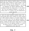
- FIG. 7 is a flowchart of an operating method for a resistive memory storage apparatus according to an embodiment of the disclosure. Please refer to FIG. 2A , FIG. 4 , FIG. 6 and FIG. 7 .
- the operating method of the exemplary embodiment is at least applicable to the resistive memory storage apparatus 100 of FIG. 2A , but the disclosure is not limited thereto. Taking the resistive memory storage apparatus 100 of FIG.
- the memory controller 130 in a step S100, during the first resistance transition phase of the writing pulse width period, the memory controller 130 provides the control voltage V1 which gradually changes to the first voltage level L1 to the control end of the first selecting transistor T1, and during the subsequent first filament stabilization phase, the memory controller 130 provides the fixed first voltage level L1 to the control end of the first selecting transistor T1, so that the writing current Id is limited to the first predetermined current value Iref1.
- the memory controller 130 provides the control voltage V1 which gradually changes to the second voltage level L2 to the control end of the first selecting transistor T1, and during the subsequent second filament stabilization phase, the memory controller 130 provides the fixed second voltage level L2 to the control end of the first selecting transistor T1, so that the writing current Id is limited to the second predetermined current value Iref2.
- the second voltage level L2 is greater than the first voltage level L1, and the second predetermined current value Iref2 is greater than the first predetermined current value Iref1.
- the description of the embodiments of FIG. 1 to FIG. 6 can provide sufficient teaching, suggestion and implementation directions for other details of the operating method of the resistive memory storage apparatus in the embodiment of the disclosure. Therefore, the details will not be repeated again.
- the operating method of the resistive memory storage apparatus in the embodiment of the disclosure at least can be applied to a single-level cell (SLC) memory storage apparatus or a multi-level cell (MLC) memory storage apparatus, which is not limited according to the disclosure.
- the operating method of the resistive memory storage apparatus in the embodiment of the disclosure can further be applied to a one-time programmable (OTP) memory storage apparatus or a multi-time programmable (MTP) memory storage apparatus, which is not limited according to the disclosure.
- OTP one-time programmable
- MTP multi-time programmable
- the memory controller applies the control voltage to the control end of the first selecting transistor.
- the writing current gradually changes to the predetermined current values during the resistance transition phases of the writing pulse width period, and the writing current is limited to one or more predetermined current values during the filament stabilization phases of the writing pulse width period.
- the cell current distribution is improved to be more uniform, and the conductive filament structure of the memory cells is improved to be more robust, so as to effectively reduce the BER.
Landscapes
- Semiconductor Memories (AREA)
- Read Only Memory (AREA)
Description
- The disclosure relates to a memory storage apparatus and an operating method thereof, and more particularly, to a resistive memory storage apparatus and an operating method thereof.
- The resistive memory (e.g. resistive random access memory (RRAM)) is advantageous in low power consumption, high-speed operation, high density and compatibility with the complementary metal oxide semiconductor (CMOS), and therefore is an adequate choice for the next generation non-volatile memory device.
- Current resistive memory includes an upper electrode and a lower electrode disposed opposite to each other and a dielectric layer between the upper electrode and the lower electrode. Before the resistive memory of the related art is repeatedly switched between a high resistance state (HRS) and a low resistance state (LRS) to memorize data, a channel forming operation is required. The forming operation includes applying a bias voltage (e.g. a positive bias) to the resistive memory, such that a current is generated and flows from the upper electrode to the lower electrode. As a result, oxygen vacancies and oxygen ions are generated in the dielectric layer to form a current path, and the resistive memory is switched from the HRS to the LRS to form a conductive filament. Generally, in the formed filament, the diameter of the portion adjacent to the upper electrode is smaller than the diameter of the portion adjacent to the lower electrode. After that, the resistive memory can be reset to the HRS, or can be set to the LRS, to complete the data memorization. In addition, when the resistive memory of the related art is reset, a bias voltage with polarity opposite to the polarity of a setting bias voltage is applied to the resistive memory, such that a current flows from the lower electrode to the upper electrode. In such a situation, the oxygen vacancies adjacent to the upper electrode combine with partial oxygen ions, which interrupts the current path. As a result, the filament is cut off at the portion adjacent to the upper electrode. When the resistive memory of the related art is set, the setting bias voltage with polarity identical to the polarity of the bias voltage of the forming operation is applied to the resistive memory, such that a current flows from the upper electrode to the lower electrode. In such a situation, the oxygen ions adjacent to the upper electrode are detached from the oxygen vacancies, and oxygen vacancies are reformed, such that the filament is reformed at the portion adjacent to the upper electrode.
- However, according to the resistive memory of the related art, during the forming operation or the setting operation of the resistive memory, a verification operation is required after applying the forming bias voltage or the setting bias voltage. The verification operation includes discharging and applying a verification voltage, and includes charging and providing the forming bias voltage or the setting bias voltage again when the verification fails. Therefore, the execution time of the forming operation or the setting operation is significantly long. In addition, according to the resistive memory of the related art, after the forming operation or the setting operation of the resistive memory, the cell current distribution is uneven since the cell variations occur during the manufacturing process, which results in a high bit error rate (BER).
-
US 2019/371399 Al discloses a resistive random access memory (RRAM) circuit and related method to limit current, or ramp voltage, applied to a source line or bitline of an RRAM array. The RRAM array has one or more source lines and one or more bitlines. A control circuit sets an RRAM cell to a low resistance state in a set operation, and resets the RRAM cell to a high resistance state in a reset operation. A voltage applied to a bitline or source line is ramped during a first time interval, held to a maximum voltage value during a second interval, and ceased after the second time interval. - The disclosure provides a resistive memory storage apparatus and an operating method thereof, which can effectively reduce the bit error rate (BER). The invention is set out in the appended set of claims. The following disclosure serves a better understanding of the present invention.
- According to the disclosure, a resistive memory storage apparatus includes a memory array, a first selecting transistor and a memory controller. The memory array includes multiple memory cells, each of which outputs a writing current during a writing pulse width period. The first selecting transistor is coupled to the memory cells. The memory controller is coupled to the first selecting transistor and the memory cells. The memory controller is utilized for applying a first control voltage gradually changing to a first voltage level according to the writing current to a control end of the first selecting transistor during a first resistance transition phase of the writing pulse width period, and is utilized for setting the first control voltage to the first voltage level during a first filament stabilization phase after the first resistance transition phase, so as to limit the writing current to a first predetermined current value. The writing pulse width period includes a plurality of resistance transition phases and a plurality of filament stabilization phases. The writing current is limited to the corresponding predetermined current value during each of the plurality of filament stabilization phases. The plurality of resistance transition phases include the first resistance transition phase and a second resistance transition phase after the first filament stabilization phase. The plurality of filament stabilization phases include the first filament stabilization phase and a second filament stabilization phase after the second resistance transition phase. The memory controller is utilized to gradually change the first control voltage to the first voltage level during the first resistance transition phase, and to gradually change the first control voltage to a second voltage level during the second resistance transition phase, and is utilized to set the first control voltage to the second voltage level during the second filament stabilization phase. The second voltage level is greater than the first voltage level. The writing current is limited to a second predetermined current value greater than the first predetermined current value during the second filament stabilization phase.
- According to the disclosure, an operating method for a resistive memory storage apparatus includes: during a writing pulse width period, reading a writing current from one of multiple memory cells, wherein the writing pulse width period includes a first resistance transition phase, a first filament stabilization phase, a second resistance transition phase and the second filament stabilization phase; during the first resistance transition phase, providing a control end of the first selecting transistor with a control voltage gradually changing to a first voltage level according to the writing current to provide the writing current to one of the memory cells; during the first filament stabilization phase after the first resistance transition phase, providing the control end of the first selecting transistor with the control voltage fixed to the first voltage level to limit the writing current to a first predetermined current value; during the second resistance transition phase after the first filament stabilization phase, providing the control end of the first selecting transistor with the control voltage gradually changing to a second voltage level greater than the first voltage level according to the writing current; and during the second filament stabilization phase after the second resistance transition phase, providing the control end of the first selecting transistor with the control voltage fixed to the second voltage level to limit the writing current to a second predetermined current value. The second predetermined current value is greater than the first predetermined current value during the second filament stabilization phase.
- Based on the foregoing, according to the embodiments of the disclosure, the memory controller applies the control voltage to the control end of the first selecting transistor. As such, the writing current gradually changes to the predetermined current values during the resistance transition phases of the writing pulse width period, and the writing current is limited to one or more predetermined current values during the filament stabilization phases of the writing pulse width period. As a result, the BER can be effectively reduced.
-
-
FIG. 1 is a schematic diagram of a resistive memory storage apparatus according to an embodiment of the disclosure. -
FIG. 2A is a schematic diagram of the resistive memory storage apparatus ofFIG. 1 . -
FIG. 2B is a block diagram of a memory controller ofFIG. 2A . -
FIG. 3 is a schematic diagram of waveforms of a writing current during a writing pulse width period according to an embodiment of the disclosure. -
FIG. 4 is a schematic diagram of waveforms of the writing current during the writing pulse width period according to an alternative embodiment of the disclosure. -
FIG. 5A, FIG. 5B, FIG. 5C and FIG. 5D are schematic diagrams illustrating filament structures of memory cells at different stages according to an embodiment of the disclosure. -
FIG. 6 is a schematic diagram illustrating voltage and current waveforms of a resistive memory storage apparatus according to an embodiment of the disclosure. -
FIG. 7 is a flowchart of an operating method for a resistive memory storage apparatus according to an embodiment of the disclosure. - Several embodiments are presented below to illustrate the disclosure. However, the disclosure is not limited to the illustrated embodiments. Also, reasonable combinations are allowed among the embodiments. The term "coupled" used in the entire specification of the disclosure (including the claims) can refer to any direct or indirect connection means. For example, if it is described that the first device is coupled to the second device, it should be interpreted that the first device can be directly connected to the second device, or the first device can be indirectly connected to the second device through other devices or some kind of connection means.
-
FIG. 1 is a schematic diagram of a resistive memory storage apparatus according to an embodiment of the disclosure. As illustrated inFIG. 1 , the resistivememory storage apparatus 100 in the embodiment includes afirst selector circuit 110, asecond selector circuit 120, amemory controller 130, and a memory array. The memory array includesmultiple memory cells 140. InFIG. 1 , merely onememory cell 140 is drawn as an example. Thememory controller 130 is configured to provide a control voltage V1 to thefirst selector circuit 110 during a writing pulse width period. The writing pulse width period includes a resistance transition phase P0 and a subsequent filament stabilization phase P1 (marked inFIG. 3 ). That is, the filament stabilization phase P1 follows the resistance transition phase P0, and there is no time interval therebetween according to an exemplary embodiment. However, the disclosure provides no limitation to whether there is any time interval between the two phases. The writing pulse width period refers to the time required for certain data to be successfully written into the selectedmemory cell 140. -
FIG. 2A is a schematic diagram of the internal of the resistive memory storage apparatus ofFIG. 1 . Please refer toFIG. 1 andFIG. 2A , in which thememory cell 140 is characterized by a (1T1R) structure including a transistor T3 and a variable resistor R, or a (2T2R) structure including two transistors and two variable resistors, implementation of which is well known to a skilled person in the art, and is not further narrated herein. Note that, the structure of thememory cell 140 is not limited according to the disclosure. - According to the embodiment, the
memory controller 130 can be a processor chip, a field-programmable gate array (FPGA) chip, a programmable controller, an application specific integrated circuit (ASIC), a programmable logic device (PLD), a device similar to these devices, a combination of these devices, or a circuit block other than these devices but functioning the same, implementation of which is well known to a skilled person in the art, and is not further narrated herein. - Specifically, one end of the
memory cell 140 is coupled to a bit line BL through thefirst selector circuit 110, and the other end of thememory cell 140 is coupled to a source line SL through thesecond selector circuit 120. According to exemplary embodiments, thefirst selector circuit 110 and thesecond selector circuit 120 can be located in the same selector circuit block, or can be implemented by different circuit blocks, the disclosure is not limited thereto. During the writing pulse width period, a control end of the transistor T3 of thememory cell 140 is provided with a voltage V3 (also called as word line voltage), a control end of a second selecting transistor T2 is provided with a voltage V2, and thememory controller 130 provides the control voltage V1 to thefirst selector circuit 110. As such, thefirst selector circuit 110 provides a writing current Id to thememory cells 140 of the memory array, and the writing current Id is provided to a first end of thesecond selector circuit 120 through thememory cell 140. Thememory controller 130 receives the writing current Id from a second end of thesecond selector circuit 120, and updates the control voltage V1 according to the writing current Id read from thesecond selector circuit 120 to output the updated control voltage V1 to thefirst selector circuit 110. As a result, the writing current Id which writes thememory cells 140 of the memory array to the same state changes to a predetermined current value during the resistance transition phase P0, and is limited to the same predetermined current value. Thememory controller 130 is further configured to continuously provide the control voltage V1 to thefirst selector circuit 110 during the filament stabilization phase P1 after the writing current Id reaches the predetermined current value, so that the writing current Id continuously passes through thememory cell 140 during the filament stabilization phase P1. - The
first selector circuit 110 includes one or more first selecting transistors T1, and thesecond selector circuit 120 includes one or more second selecting transistors T2. According toFIG. 2A , merely one selecting transistor is drawn in each of the selector circuits for illustration, but the number of the selecting transistor is not limited according to the disclosure. Specifically, the first end of the first selecting transistor T1 is coupled to the bit line BL, and the second end of the first selecting transistor T1 is coupled to thememory cell 140. The control end of the first selecting transistor T1 is coupled to thememory controller 130. The first end of the second selecting transistor T2 is coupled to thememory cell 140. The second end of the second selecting transistor T2 is coupled to the source line SL and thememory controller 130. -
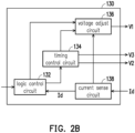
FIG. 2B is a functional block diagram of the memory controller ofFIG. 2A . As illustrated inFIG. 2B , thememory controller 130 in the embodiment includes alogic control circuit 132, atiming control circuit 134, a voltage adjustcircuit 136 and acurrent sense circuit 138. Thelogic control circuit 132 functions as the core of thememory controller 130, and is configured to receive multiple setting values (such as the setting of the predetermined current value, the setting of the step number, and the setting of the length of time of the filament stabilization phase). In addition, thelogic control circuit 132 is configured to compare the writing current Id output from thecurrent sense circuit 138, and control the operations of thetiming control circuit 134 and the voltage adjustcircuit 136 according to the writing current Id and the setting values. The voltage adjustcircuit 136 is configured to adjust and output the control voltage V1 according to the writing current Id, the output of thelogic control circuit 132 and the output of thetiming control circuit 134. Thetiming control circuit 134 is configured to control the feedback timing and control timing of the signals. Thecurrent sense circuit 138 is configured to detect the writing current Id and outputting the writing current Id to thelogic control circuit 132. According to an exemplary embodiment, the voltage adjustcircuit 136 and thecurrent sense circuit 138 are analog. -
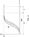
FIG. 3 is a schematic diagram of waveforms of the writing current during the writing pulse width period according to an embodiment of the disclosure. In the embodiment, during the writing pulse width period T_WPW, thememory controller 130 provides an initial control voltage V1i to thefirst selector circuit 110, so that thefirst selector circuit 110 provides the writing current Id to thememory cells 140 of the memory array. The resistance value of each of thememory cells 140 varies in response to the writing current Id. Thememory controller 130 reads the writing current Id from thememory cell 140, and applies the updated control voltage V1 to the control end of first selecting transistor T1 according to the writing current Id read from thememory cell 140. After the writing current Id which writes thememory cells 140 of the memory array to the same state exceeds a predetermined current value Iref, thememory controller 130 sets the corresponding control voltage V1 to a fixed control voltage V1f, and continuously provides the fixed control voltage V1f to the control end of the first selecting transistor T1 during the filament stabilization phase P1. As such, the writing current Id of thememory cells 140 is limited to the predetermined current value Iref during the filament stabilization phase P1, so as to complete the write operation. According to the embodiment, during the resistance transition phase P0, the control voltage V1 provided by thememory controller 130 gradually increases from the initial control voltage V1i to the fixed control voltage V1f, so that the current read from the respective memory cell 140 (i.e. the writing current Id) gradually increases with the control voltage V1. According to an embodiment, as shown inFIG. 6 , during the resistance transition phase P0, the control voltage V1 provided by thememory controller 130 gradually increases from the initial control voltage V1i to a final control voltage V1t greater than the fixed control voltage V1f. As such, the current read by the respective memory cell 140 (i.e. the writing current Id) gradually increases with the increase of the control voltage V1, so as to be greater than the predetermined current value Iref. And, after reaching the final control voltage V1t, the control voltage V1 provided by thememory controller 130 gradually decreases to the fixed control voltage V1f. As a result, the current read from the respective memory cell 140 (i.e. the writing current Id) decreases with the decrease of the control voltage V1, so as to be equal to the predetermined current value Iref. - In a practical situation, after the forming operation or the setting operation is performed on the memory cell, an uneven distribution of the cell currents may appear and result in a high bit error rate (BER). The uneven distribution is caused by manufacturing process variations of the memory cells. In addition, due to the manufacturing process variations, the writing
currents 300 read from different memory cells are different during the writing pulse width period T_WPW, as shown inFIG. 3 . According to the embodiment of the disclosure, by limiting the writing currents Id which write the memory array to the same state to the predetermined current value Iref, the cell current distribution can be more uniform. In addition, by continuously providing the fixed control voltage V1f to the control end of first selecting transistor T1 during the filament stabilization phase P1, the conductive filament structure of the memory cells are enhanced to be more robust, so as to effectively reduce the BER. Moreover, according to the embodiment, the memory controller can complete the writing operation without a verification operation, that is, a writing verification operation is not performed during the writing pulse width period, so that the time required for writing can be shortened. -
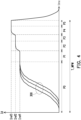
FIG. 4 is a schematic diagram of waveforms of the writing current during the writing pulse width period according to an alternative embodiment of the disclosure. In the embodiment, the writing pulse width period T_WPW includes multiple resistance transition phases and subsequent filament stabilization phases. Thememory controller 130 provides the increasing control voltage V1 to the control end of the first selecting transistor T1 during each of the resistance transition phases, and the initial control voltage of the previous resistance transition phase is smaller than the initial control voltage of the next resistance transition phase. As such, the writing current Id gradually increases from a predetermined current value Iref1 to predetermined current values Iref2 and Iref3. Note that, the predetermined current value Iref3 is greater than the predetermined current value Iref2, and the predetermined current value Iref2 is greater than the predetermined current value Iref1. The number of the aforementioned predetermined current values is not limited according to the disclosure. - For example, the writing pulse width period T_WPW includes resistance transition phases P0, P2, P4 and subsequent filament stabilization phases P1, P3, P5 following the resistance transition phase. The
memory controller 130 provides the increasing control voltage V1 to the control end of the first selecting transistor T1 during the resistance transition phase P0, so that the writing current Id gradually increases to the predetermined current value Iref1 during the resistance transition phase P0, and is finally limited to the predetermined current value Iref1 (first predetermined current value). Next, as shown inFIG. 6 , thememory controller 130 provides the fixed control voltage V1f to the control end of the first selecting transistor T1 during the filament stabilization phase P1, so that the writing current Id is maintained at the predetermined current value Iref1 during the filament stabilization phase P1. Note that, the length of the filament stabilization phase P1 is shorter than the length of the resistance transition phase P0. Next, thememory controller 130 provides an increasing control voltage V1' to the control end of the first selecting transistor T1 during the resistance transition phase P2, so that the writing current Id gradually increases to the predetermined current value Iref2 during the resistance transition phase P2, and is finally limited to the predetermined current value Iref2 (second predetermined current value). Next, as shown inFIG. 6 , thememory controller 130 provides a fixed control voltage V1'f to the control end of the first selecting transistor T1 during the filament stabilization phase P3, so that the writing current Id is maintained at the predetermined current value Iref2 during the filament stabilization phase P3. Note that, the predetermined current value Iref2 is greater than the predetermined current value Iref1. Also, the length of the filament stabilization phase P3 is shorter than the length of the resistance transition phase P2. Similarly, thememory controller 130 provides an increasing control voltage V1" to the control end of the first selecting transistor T1 during the resistance transition phase P4, so that the writing current Id gradually increases to the predetermined current value Iref3 during the resistance transition phase P4, and is finally limited to the predetermined current value Iref3 (third predetermined current value). Next, as shown inFIG. 6 , thememory controller 130 provides a fixed control voltage V1"f to the control end of the first selecting transistor T1 during the filament stabilization phase P5, so that the writing current Id is maintained at the predetermined current value Iref3 during the filament stabilization phase P5. Note that, the predetermined current value Iref3 is greater than the predetermined current value Iref2. Also, the length of the filament stabilization phase P5 is shorter than the length of the resistance transition phase P4. -
FIG. 5A to FIG. 5D are schematic diagrams illustrating filament distributions of the memory cells at different stages according to an embodiment of the disclosure. As shown inFIG. 4 andFIG. 5A to FIG. 5D , during the resistance transition phase P0, transitions occur in thememory cells 140. For example, please refer toFIG. 5A , in which the transition is from a high resistance state (HRS) to a low resistance state (LRS), and the filament distribution is relatively loose. After the transition, thememory controller 130 continuously applies the fixed control voltage V1f to the control end of the first selecting transistor T1, so that the writing current Id is limited to the predetermined current value Iref1 during the filament stabilization phase P1, and thereby the filament distribution of thememory cells 140 changes to a stabilization state during the filament stabilization phase P1, as shown inFIG. 5B . Next, during the resistance transition phase P2, by providing the increasing control voltage V1' to the control end of the first selecting transistor T1, the filament in the loose state is rebuilt or restored, as shown inFIG. 5C . InFIG. 5C , E represents the direction of the electric field, and e- represents the movement direction of electron. Next, during the filament stabilization phase P3, by continuously applying the fixed control voltage V1'f to the control end of the first selecting transistor T1, the filament distribution of thememory cells 140 become stable again, as shown inFIG. 5D . - Similarly, during the resistance transition phase P4, the filament distribution of the
memory cells 140 is in a relatively loose state. During the filament stabilization phase P5, the filament distribution of thememory cells 140 becomes stable again. That is to say, according to the embodiment, by applying the stepping control voltages V1, V1', V1'' to the control end of the first selecting transistor T1, the writing current Id gradually increases to the predetermined current values Iref1, Iref2, Iref3 during the respective resistance transition phases P0, P2, P4, and is respectively limited to the predetermined current values Iref1, Iref2, Iref3 during the filament stabilization phases P1, P3, P5. In this way, thememory cells 140 are repeatedly switched between the loose and stable states of the filament distribution, which can enhance the filament to be more robust, and can more uniformly distribute the cell currents, so as to reduce the BER. - In the embodiment of
FIG. 4 , the predetermined current values varies in the three-step, however the disclosure is not limited to this. The number and size of the predetermined current values can be adjusted based on practical design requirements. For example, in the embodiment ofFIG. 3 , thememory controller 130 merely limits the writing current Id to the predetermined current value Iref, which is a one-step process. -
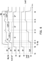
FIG. 6 is a schematic diagram illustrating voltage and current waveforms of the resistive memory storage apparatus according to an embodiment of the disclosure. Please refer toFIG. 2A andFIG. 6 . InFIG. 6 , the voltages V1, V1', V1" are the control voltages applied to the control end of first selecting transistor T1, the voltage V2 is another control voltage applied to the control end of the second selecting transistor T2 voltage, and the voltage V3 is the word line voltage applied to the control end of the transistor T3 of thememory cell 140. Voltages VBL and VSL are the respective voltages applied to the bit line BL and the source line SL. The voltages V2, V3, VBL, VSL can be provided by thememory controller 130 or other memory controllers or power suppliers of thememory storage apparatus 100. A voltage Vd is the voltage of the second end of the first selecting transistor T1. - At a time point TA, the
memory storage apparatus 100 is in an initial state, and the voltages V1, V2, V3, VBL, VSL are all 0 volts. At a time point TB, the voltages V2 and V3 are pulled high to simultaneously turn on the second selecting transistor T2 and transistor T3, and enable the second selecting transistor T2 and transistor T3 to be fully ON. For example, apply the high voltage V2 to the control end of second selecting transistor T2, and apply a low voltage (such as a ground voltage) to the source line SL to fully turn on second selecting transistor T2. In addition, the word line voltage V3 with high potential is applied to the control end of the transistor T3 of thememory cell 140 to fully turn on the transistor T3 of thememory cell 140. At a time point TC, the voltage VBL is pulled high to pull the voltage of the first end of first selecting transistor T1 to the voltage VBL. The level of the voltage VBL can be set higher to avoid clamping the writing current Id. - At a time point t0, according to the predetermined current value Iref1, the
memory controller 130 applies the increasing control voltage V1 to the control end of the first selecting transistor T1, so that the first selecting transistor T1 is turned on. From a time point t0a to a time point t1 (resistance transition phase), a transition occurs in thememory cell 140 according to the control voltage V1 and the voltage VBL, and at the time point t1, thememory controller 130 reduces the control voltage V1 to a fixed first voltage level L1, so that the writing current Id is limited to the predetermined current value Iref1, which is maintained until a time point t2. In order to stabilize the filament, the time length that the fixed first voltage level L1 is applied (filament stabilization phase) can be adjusted based on practical requirements. According to an exemplary embodiment, the interval between the time point t0 and the time point t1 are picoseconds. According to an exemplary embodiment, the length of the filament stabilization phase (i.e. the time length that the fixed first voltage level L1 is applied) is greater than the length of the resistance transition phase (i.e. the interval between the time point t0a and the time point t1). - At the time point t2, according to the predetermined current value Iref2, the
memory controller 130 gradually increases the control voltage V1' to be greater than a second voltage level L2. Note that, in the embodiment, the predetermined current value Iref2 is greater than the predetermined current value Iref1, and the second voltage level L2 is greater than the first voltage level L1. The interval between the time point t2 to a time point t3 is the resistance transition phase, in which the filament is loose and waits for reconstruction or recovery. - Similarly, from the time point t3 to a time point t4, the control voltage V1' reduces to the fixed second voltage level L2, so that the writing current Id is limited to the predetermined current value Iref2, and the
memory cell 140 is stable again. Similarly, from the time point t4 to a time point t5 (resistance transition phase), thememory controller 130 gradually increases the control voltage V1" to be greater than a third voltage level L3 according to the predetermined current value Iref3, and the filament of thememory cell 140 is loose again. From the time point t5 to a time point t6, the control voltage V1" reduces to the fixed third voltage level L3, so that the writing current Id is limited to the predetermined current value Iref3, and thememory cell 140 is stable again. Note that, the predetermined current value Iref3 is greater than the predetermined current value Iref2, and the third voltage level L3 is greater than the second voltage level L2. That is to say, in the embodiment, the control voltages V1, V1', V1" are step voltages which gradually increase over time from the first voltage level L1 to the second voltage level L2, and then increase to the third voltage level L3 in sequence. -
FIG. 7 is a flowchart of an operating method for a resistive memory storage apparatus according to an embodiment of the disclosure. Please refer toFIG. 2A ,FIG. 4 ,FIG. 6 andFIG. 7 . The operating method of the exemplary embodiment is at least applicable to the resistivememory storage apparatus 100 ofFIG. 2A , but the disclosure is not limited thereto. Taking the resistivememory storage apparatus 100 ofFIG. 2A as an example, in a step S100, during the first resistance transition phase of the writing pulse width period, thememory controller 130 provides the control voltage V1 which gradually changes to the first voltage level L1 to the control end of the first selecting transistor T1, and during the subsequent first filament stabilization phase, thememory controller 130 provides the fixed first voltage level L1 to the control end of the first selecting transistor T1, so that the writing current Id is limited to the first predetermined current value Iref1. In a step S110, during the second resistance transition phase of the writing pulse width period, thememory controller 130 provides the control voltage V1 which gradually changes to the second voltage level L2 to the control end of the first selecting transistor T1, and during the subsequent second filament stabilization phase, thememory controller 130 provides the fixed second voltage level L2 to the control end of the first selecting transistor T1, so that the writing current Id is limited to the second predetermined current value Iref2. Note that, the second voltage level L2 is greater than the first voltage level L1, and the second predetermined current value Iref2 is greater than the first predetermined current value Iref1. - In addition, the description of the embodiments of
FIG. 1 to FIG. 6 can provide sufficient teaching, suggestion and implementation directions for other details of the operating method of the resistive memory storage apparatus in the embodiment of the disclosure. Therefore, the details will not be repeated again. Moreover, the operating method of the resistive memory storage apparatus in the embodiment of the disclosure at least can be applied to a single-level cell (SLC) memory storage apparatus or a multi-level cell (MLC) memory storage apparatus, which is not limited according to the disclosure. The operating method of the resistive memory storage apparatus in the embodiment of the disclosure can further be applied to a one-time programmable (OTP) memory storage apparatus or a multi-time programmable (MTP) memory storage apparatus, which is not limited according to the disclosure. - To sum up, according to the embodiments of the disclosure, the memory controller applies the control voltage to the control end of the first selecting transistor. As such, the writing current gradually changes to the predetermined current values during the resistance transition phases of the writing pulse width period, and the writing current is limited to one or more predetermined current values during the filament stabilization phases of the writing pulse width period. By limiting the writing current to one or more predetermined current values during the filament stabilization phases, the cell current distribution is improved to be more uniform, and the conductive filament structure of the memory cells is improved to be more robust, so as to effectively reduce the BER.
Claims (12)
- A resistive memory storage apparatus (100), comprising:a memory array, comprising a plurality of memory cells (140), wherein each of the plurality of memory cells (140) outputs a writing current (Id, 300) during a writing pulse width period (T_WPW);a first selecting transistor (T1), coupled to the plurality of memory cells (140), wherein the first selecting transistor (T1) comprises a control end; anda memory controller (130), coupled to the first selecting transistor (T1) and the plurality of memory cells (140), configured to apply a first control voltage (V1) gradually changing to a first voltage level (L1) according to the writing current (Id, 300) to the control end of the first selecting transistor (T1) during a first resistance transition phase (P0) of the writing pulse width period (T_WPW), and set the first control voltage (V1) to the first voltage level (L1) during a first filament stabilization phase (P1) after the first resistance transition phase (P0), so as to limit the writing current (Id, 300) to a first predetermined current value (Iref1),wherein the resistive memory storage apparatus (100) is characterized in that the writing pulse width period (T_WPW) comprises a plurality of resistance transition phases (P0, P2, P4) and a plurality of filament stabilization phases (P1, P3, P5), and the writing current (Id, 300) is limited to the corresponding predetermined current value (Irefl, Iref2, Iref3) during each of the plurality of filament stabilization phases (P1, P3, P5),the plurality of resistance transition phases (P0, P2, P4) comprise the first resistance transition phase (P0) and a second resistance transition phase (P2) after the first filament stabilization phase (P1), the plurality of filament stabilization phases (P1, P3, P5) comprise the first filament stabilization phase (P1) and a second filament stabilization phase (P3) after the second resistance transition phase (P2), the memory controller (130) is configured to gradually change the first control voltage (V1) to the first voltage level (L1) during the first resistance transition phase (P0), and to gradually change the first control voltage (V1') to a second voltage level (L2) during the second resistance transition phase (P2), and is configured to set the first control voltage (V1') to the second voltage level (L2) during the second filament stabilization phase (P3), wherein the second voltage level (L2) is greater than the first voltage level (L1),the writing current (Id, 300) is limited to a second predetermined current value (Iref2) greater than the first predetermined current value (Iref1) during the second filament stabilization phase (P3).
- The resistive memory storage apparatus (100) of claim 1, wherein the memory controller (130) is configured to gradually increase the first control voltage (V1) from an initial control voltage (V1i) to a final control voltage (V1t) during the first resistance transition phase (P0), and the final control voltage (V1t) is greater than the first voltage level (L1).
- The resistive memory storage apparatus (100) of claim 1, further comprising a second selecting transistor (T2) coupled to the plurality of memory cells (140) and the memory controller (130),wherein the second selecting transistor (T2) comprises a first end, a second end and a control end, the first end of the second selecting transistor (T2) is coupled to the plurality of memory cells (140), the second end of the second selecting transistor (T2) is coupled to a source line (SL), and the writing current (Id, 300) is output from the second end of the second selecting transistor (T2) to the memory controller (130),wherein the first selecting transistor (T1) further comprises a first end and a second end, the first end of the first selecting transistor (T1) is coupled to a bit line (BL), the second end of the first selecting transistor (T1) is coupled to the plurality of memory cells (140), and the first selecting transistor (T1) provides the writing current (Id, 300) to one of the plurality of memory cells (140) according to the first control voltage,wherein each of the plurality of memory cells (140) comprises a transistor (T3) and a variable resistor (R),wherein the memory controller (130) is configured to provide the second selecting transistor (T2) with a first saturation voltage (V2) for fully turning on the second selecting transistor (T2) during the writing pulse width period (T_WPW), and provide the transistor (T3) with a second saturation voltage (V3) for fully turning on the transistor (T3) during the writing pulse width period (T_WPW).
- The resistive memory storage apparatus (100) of claim 3, wherein the memory controller (130) comprises:a logic control circuit (132), configured to receive a setting of the first predetermined current value (Iref1), a setting of the length of the first filament stabilization phase (P1), and receive the writing current (Id, 300);a timing control circuit (134), configured to output the first saturation voltage (V2) applied to the control end of the second selecting transistor (T2), and output the second saturation voltage (V3) applied to a control end of the transistor (T3);a voltage adjust circuit (136), configured to update a voltage level of the first control voltage (V1) according to the output of the logic control circuit (132), the output of the timing control circuit (134) and the writing current (Id, 300), and output the updated first control voltage (V1) to the control end of the first selecting transistor (T1); anda current sense circuit (138), configured to detect the writing current (Id, 300) and output the writing current (Id, 300) to the logic control circuit (132).
- The resistive memory storage apparatus (100) of claim 1, wherein the memory controller (130) is configured to set the length of the first filament stabilization phase (P1) to be shorter than the length of the first resistance transition phase (P0).
- The resistive memory storage apparatus (100) of claim 1, wherein the memory controller (130) is configured to set the length of the first filament stabilization phase (P1) to be longer than the length of the first resistance transition phase (P0).
- The resistive memory storage apparatus (100) of claim 1, wherein the memory controller (130) is configured to complete a writing operation during the writing pulse width period (T_WPW) without a verification operation.
- An operating method for a resistive memory storage apparatus (100), wherein the resistive memory storage apparatus (100) comprises a plurality of memory cells (140) and a first selecting transistor (T1) coupled to the plurality of memory cells (140), the operation method being characterized by comprising:during a writing pulse width period (T_WPW), reading a writing current (Id, 300) from one of the plurality of memory cells (140), wherein the writing pulse width period (T_WPW) comprises a plurality of resistance transition phases (P0, P2, P4) and a plurality of filament stabilization phases (P1, P3, P5), the plurality of resistance transition phases (P0, P2, P4) comprise a first resistance transition phase (P0) and a second resistance transition phase (P2) after the first filament stabilization phase (P1), and the plurality of filament stabilization phases (P1, P3, P5) comprise a first filament stabilization phase (P1) and a second filament stabilization phase (P3) after the second resistance transition phase (P2);during the first resistance transition phase (P0), providing a control end of the first selecting transistor (T1) with a control voltage (V1) gradually changing to a first voltage level (L1) according to the writing current (Id, 300) to provide the writing current (Id, 300) to one of the plurality of memory cells (140);during the first filament stabilization phase (P1) after the first resistance transition phase (P0), providing the control end of the first selecting transistor (T1) with the control voltage (V1) fixed to the first voltage level (L1) to limit the writing current (Id, 300) to a first predetermined current value (Irefl);during the second resistance transition phase (P2) after the first filament stabilization phase (P1), providing the control end of the first selecting transistor (T1) with the control voltage (V1') gradually changing to a second voltage level (L2) greater than the first voltage level (L1) according to the writing current (Id, 300); andduring the second filament stabilization phase (P3) after the second resistance transition phase (P2), providing the control end of the first selecting transistor (T1) with the control voltage (V1') fixed to the second voltage level (L2) to limit the writing current (Id, 300) to a second predetermined current value (Iref2),wherein the second predetermined current value (Iref2) is greater than the first predetermined current value (Iref1) during the second filament stabilization phase (P3).
- The operating method of claim 8, wherein the resistive memory storage apparatus (100) further comprises a second selecting transistor (T2), and each of the plurality of memory cells (140) is disposed between the first selecting transistor (T1) and the second selecting transistor (T2), the operating method further comprising:
during the writing pulse width period (T_WPW), providing the second selecting transistor (T2) with a first saturation voltage (V2) for fully turning on the second selecting transistor (T2), and providing a transistor (T3) of one of the plurality of memory cells (140) with a second saturation voltage (V3) for fully turning on the transistor (T3) during the writing pulse width period (T_WPW). - The operating method of claim 8, wherein the step of providing the control end of the first selecting transistor (T1) with the control voltage (V1) gradually changing to the first voltage level (L1) according to the writing current (Id, 300) comprises:
during the first resistance transition phase (P0), gradually increasing the control voltage (V1) from an initial control voltage (V1i) to a final control voltage (V1t), wherein the final control voltage (V1t) is greater than the first voltage level (L1). - The operating method of claim 8, further comprising:
setting the first predetermined current value (Iref1), the second predetermined current value (Iref2), the length of the first filament stabilization phase (P1) and the number of the plurality of resistance transition phases (P0, P2, P4), wherein the length of the first filament stabilization phase (P1) is shorter than the length of the first resistance transition phase (P0). - The operating method of claim 8, wherein a verification operation is not performed during the writing pulse width period (T_WPW).
Applications Claiming Priority (1)
| Application Number | Priority Date | Filing Date | Title |
|---|---|---|---|
| TW109113857A TWI751537B (en) | 2020-04-24 | 2020-04-24 | Resistive memory storage apparatus and operating method thereof |
Publications (3)
| Publication Number | Publication Date |
|---|---|
| EP3901953A1 EP3901953A1 (en) | 2021-10-27 |
| EP3901953B1 true EP3901953B1 (en) | 2025-01-22 |
| EP3901953C0 EP3901953C0 (en) | 2025-01-22 |
Family
ID=75529830
Family Applications (1)
| Application Number | Title | Priority Date | Filing Date |
|---|---|---|---|
| EP21168292.7A Active EP3901953B1 (en) | 2020-04-24 | 2021-04-14 | Resistive memory storage apparatus and operating method thereof |
Country Status (5)
| Country | Link |
|---|---|
| US (1) | US11437101B2 (en) |
| EP (1) | EP3901953B1 (en) |
| KR (1) | KR102476448B1 (en) |
| ES (1) | ES3014733T3 (en) |
| TW (1) | TWI751537B (en) |
Families Citing this family (1)
| Publication number | Priority date | Publication date | Assignee | Title |
|---|---|---|---|---|
| EP4099327A1 (en) * | 2021-06-04 | 2022-12-07 | Commissariat à l'Energie Atomique et aux Energies Alternatives | Method for programming an array of resistive memory cells |
Family Cites Families (11)
| Publication number | Priority date | Publication date | Assignee | Title |
|---|---|---|---|---|
| KR100558548B1 (en) * | 2003-11-27 | 2006-03-10 | 삼성전자주식회사 | Light Driver Circuit and Light Current Application Method in Phase Change Memory Devices |
| JPWO2007023569A1 (en) * | 2005-08-26 | 2009-03-26 | 富士通株式会社 | Nonvolatile semiconductor memory device and writing method thereof |
| KR100868105B1 (en) | 2006-12-13 | 2008-11-11 | 삼성전자주식회사 | Resistance memory device |
| JP5062251B2 (en) | 2007-03-28 | 2012-10-31 | 富士通株式会社 | Variable resistance memory and data writing method thereof |
| US7869258B2 (en) | 2008-06-27 | 2011-01-11 | Sandisk 3D, Llc | Reverse set with current limit for non-volatile storage |
| TWI482155B (en) * | 2010-07-05 | 2015-04-21 | Macronix Int Co Ltd | Nonvolatile memory device having trasistor connected in parallel with resistance switching device |
| US20120230081A1 (en) | 2011-03-10 | 2012-09-13 | International Business Machines Corporation | Cell-state measurement in resistive memory |
| JP5404683B2 (en) | 2011-03-23 | 2014-02-05 | 株式会社東芝 | Resistance change memory |
| US20160148681A1 (en) * | 2014-11-20 | 2016-05-26 | Infineon Technologies Ag | Parallel forming of memory cells |
| US9691478B1 (en) | 2016-04-22 | 2017-06-27 | Macronix International Co., Ltd. | ReRAM array configuration for bipolar operation |
| JP6857257B2 (en) | 2017-01-20 | 2021-04-14 | ヘフェイ リライアンス メモリー リミティド | RRAM write |
-
2020
- 2020-04-24 TW TW109113857A patent/TWI751537B/en active
-
2021
- 2021-04-08 US US17/226,052 patent/US11437101B2/en active Active
- 2021-04-14 EP EP21168292.7A patent/EP3901953B1/en active Active
- 2021-04-14 ES ES21168292T patent/ES3014733T3/en active Active
- 2021-04-20 KR KR1020210051009A patent/KR102476448B1/en active Active
Also Published As
| Publication number | Publication date |
|---|---|
| US11437101B2 (en) | 2022-09-06 |
| TW202141492A (en) | 2021-11-01 |
| TWI751537B (en) | 2022-01-01 |
| EP3901953A1 (en) | 2021-10-27 |
| KR102476448B1 (en) | 2022-12-12 |
| KR20210132604A (en) | 2021-11-04 |
| US20210335421A1 (en) | 2021-10-28 |
| EP3901953C0 (en) | 2025-01-22 |
| ES3014733T3 (en) | 2025-04-24 |
Similar Documents
| Publication | Publication Date | Title |
|---|---|---|
| US10991427B2 (en) | Memory programming methods and memory systems | |
| JP4187197B2 (en) | Method for controlling semiconductor memory device | |
| CN100472647C (en) | non-volatile semiconductor storage device | |
| US10783961B2 (en) | Memory cells, memory systems, and memory programming methods | |
| EP3471101B1 (en) | Devices for accessing resistive change elements in resistive change element arrays | |
| CN107305783B (en) | Memory device and method for bipolar operation | |
| US8411487B2 (en) | Semiconductor memory device | |
| US9627060B2 (en) | Memory circuit and method of programming memory circuit | |
| US12176028B2 (en) | Resistive change element arrays | |
| US20210319819A1 (en) | Non-volatile memory with multiplexer transistor regulator circuit | |
| US11437101B2 (en) | Resistive memory storage apparatus and operating method thereof | |
| CN106653079A (en) | Resistive memory device and writing method thereof | |
| KR20090000407A (en) | Voltage providing device and flash memory device having same | |
| CN113628651B (en) | Resistive memory storage device and operation method thereof | |
| JP6906660B1 (en) | Resistive random access memory storage device and its operation method | |
| CN109509496B (en) | How to operate a resistive memory element | |
| TW201737254A (en) | Writing method for resistive memory cell and resistive memory | |
| CN109658963B (en) | Operation method of resistive memory storage device | |
| JP2009259336A (en) | Semiconductor device and its control method | |
| TWI645403B (en) | Resistive memory apparatus and operating method thereof | |
| CN121725850A (en) | Programming of high resistance state HRS of resistive memory element | |
| CN116325512A (en) | memristive logic gate |
Legal Events
| Date | Code | Title | Description |
|---|---|---|---|
| PUAI | Public reference made under article 153(3) epc to a published international application that has entered the european phase |
Free format text: ORIGINAL CODE: 0009012 |
|
| STAA | Information on the status of an ep patent application or granted ep patent |
Free format text: STATUS: REQUEST FOR EXAMINATION WAS MADE |
|
| 17P | Request for examination filed |
Effective date: 20210414 |
|
| AK | Designated contracting states |
Kind code of ref document: A1 Designated state(s): AL AT BE BG CH CY CZ DE DK EE ES FI FR GB GR HR HU IE IS IT LI LT LU LV MC MK MT NL NO PL PT RO RS SE SI SK SM TR |
|
| B565 | Issuance of search results under rule 164(2) epc |
Effective date: 20210908 |
|
| RBV | Designated contracting states (corrected) |
Designated state(s): AL AT BE BG CH CY CZ DE DK EE ES FI FR GB GR HR HU IE IS IT LI LT LU LV MC MK MT NL NO PL PT RO RS SE SI SK SM TR |
|
| STAA | Information on the status of an ep patent application or granted ep patent |
Free format text: STATUS: EXAMINATION IS IN PROGRESS |
|
| 17Q | First examination report despatched |
Effective date: 20230605 |
|
| GRAP | Despatch of communication of intention to grant a patent |
Free format text: ORIGINAL CODE: EPIDOSNIGR1 |
|
| STAA | Information on the status of an ep patent application or granted ep patent |
Free format text: STATUS: GRANT OF PATENT IS INTENDED |
|
| INTG | Intention to grant announced |
Effective date: 20240913 |
|
| GRAS | Grant fee paid |
Free format text: ORIGINAL CODE: EPIDOSNIGR3 |
|
| GRAA | (expected) grant |
Free format text: ORIGINAL CODE: 0009210 |
|
| STAA | Information on the status of an ep patent application or granted ep patent |
Free format text: STATUS: THE PATENT HAS BEEN GRANTED |
|
| AK | Designated contracting states |
Kind code of ref document: B1 Designated state(s): AL AT BE BG CH CY CZ DE DK EE ES FI FR GB GR HR HU IE IS IT LI LT LU LV MC MK MT NL NO PL PT RO RS SE SI SK SM TR |
|
| REG | Reference to a national code |
Ref country code: GB Ref legal event code: FG4D |
|
| REG | Reference to a national code |
Ref country code: CH Ref legal event code: EP |
|
| REG | Reference to a national code |
Ref country code: IE Ref legal event code: FG4D |
|
| REG | Reference to a national code |
Ref country code: DE Ref legal event code: R096 Ref document number: 602021025049 Country of ref document: DE |
|
| U01 | Request for unitary effect filed |
Effective date: 20250130 |
|
| U07 | Unitary effect registered |
Designated state(s): AT BE BG DE DK EE FI FR IT LT LU LV MT NL PT RO SE SI Effective date: 20250206 |
|
| REG | Reference to a national code |
Ref country code: ES Ref legal event code: FG2A Ref document number: 3014733 Country of ref document: ES Kind code of ref document: T3 Effective date: 20250424 |
|
| U20 | Renewal fee for the european patent with unitary effect paid |
Year of fee payment: 5 Effective date: 20250424 |
|
| PG25 | Lapsed in a contracting state [announced via postgrant information from national office to epo] |
Ref country code: RS Free format text: LAPSE BECAUSE OF FAILURE TO SUBMIT A TRANSLATION OF THE DESCRIPTION OR TO PAY THE FEE WITHIN THE PRESCRIBED TIME-LIMIT Effective date: 20250422 |
|
| PG25 | Lapsed in a contracting state [announced via postgrant information from national office to epo] |
Ref country code: PL Free format text: LAPSE BECAUSE OF FAILURE TO SUBMIT A TRANSLATION OF THE DESCRIPTION OR TO PAY THE FEE WITHIN THE PRESCRIBED TIME-LIMIT Effective date: 20250122 |
|
| PGFP | Annual fee paid to national office [announced via postgrant information from national office to epo] |
Ref country code: ES Payment date: 20250513 Year of fee payment: 5 Ref country code: GB Payment date: 20250422 Year of fee payment: 5 |
|
| PG25 | Lapsed in a contracting state [announced via postgrant information from national office to epo] |
Ref country code: NO Free format text: LAPSE BECAUSE OF FAILURE TO SUBMIT A TRANSLATION OF THE DESCRIPTION OR TO PAY THE FEE WITHIN THE PRESCRIBED TIME-LIMIT Effective date: 20250422 Ref country code: IS Free format text: LAPSE BECAUSE OF FAILURE TO SUBMIT A TRANSLATION OF THE DESCRIPTION OR TO PAY THE FEE WITHIN THE PRESCRIBED TIME-LIMIT Effective date: 20250522 |
|
| PG25 | Lapsed in a contracting state [announced via postgrant information from national office to epo] |
Ref country code: HR Free format text: LAPSE BECAUSE OF FAILURE TO SUBMIT A TRANSLATION OF THE DESCRIPTION OR TO PAY THE FEE WITHIN THE PRESCRIBED TIME-LIMIT Effective date: 20250122 |
|
| PG25 | Lapsed in a contracting state [announced via postgrant information from national office to epo] |
Ref country code: GR Free format text: LAPSE BECAUSE OF FAILURE TO SUBMIT A TRANSLATION OF THE DESCRIPTION OR TO PAY THE FEE WITHIN THE PRESCRIBED TIME-LIMIT Effective date: 20250423 |
|
| PG25 | Lapsed in a contracting state [announced via postgrant information from national office to epo] |
Ref country code: SM Free format text: LAPSE BECAUSE OF FAILURE TO SUBMIT A TRANSLATION OF THE DESCRIPTION OR TO PAY THE FEE WITHIN THE PRESCRIBED TIME-LIMIT Effective date: 20250122 |
|
| PG25 | Lapsed in a contracting state [announced via postgrant information from national office to epo] |
Ref country code: CZ Free format text: LAPSE BECAUSE OF FAILURE TO SUBMIT A TRANSLATION OF THE DESCRIPTION OR TO PAY THE FEE WITHIN THE PRESCRIBED TIME-LIMIT Effective date: 20250122 |
|
| PG25 | Lapsed in a contracting state [announced via postgrant information from national office to epo] |
Ref country code: SK Free format text: LAPSE BECAUSE OF FAILURE TO SUBMIT A TRANSLATION OF THE DESCRIPTION OR TO PAY THE FEE WITHIN THE PRESCRIBED TIME-LIMIT Effective date: 20250122 |
|
| REG | Reference to a national code |
Ref country code: CH Ref legal event code: H13 Free format text: ST27 STATUS EVENT CODE: U-0-0-H10-H13 (AS PROVIDED BY THE NATIONAL OFFICE) Effective date: 20251125 |
|
| PLBE | No opposition filed within time limit |
Free format text: ORIGINAL CODE: 0009261 |
|
| STAA | Information on the status of an ep patent application or granted ep patent |
Free format text: STATUS: NO OPPOSITION FILED WITHIN TIME LIMIT |
|
| PG25 | Lapsed in a contracting state [announced via postgrant information from national office to epo] |
Ref country code: MC Free format text: LAPSE BECAUSE OF FAILURE TO SUBMIT A TRANSLATION OF THE DESCRIPTION OR TO PAY THE FEE WITHIN THE PRESCRIBED TIME-LIMIT Effective date: 20250122 |
|
| 26N | No opposition filed |
Effective date: 20251023 |
|
| PG25 | Lapsed in a contracting state [announced via postgrant information from national office to epo] |
Ref country code: CH Free format text: LAPSE BECAUSE OF NON-PAYMENT OF DUE FEES Effective date: 20250430 |
|
| PG25 | Lapsed in a contracting state [announced via postgrant information from national office to epo] |
Ref country code: IE Free format text: LAPSE BECAUSE OF NON-PAYMENT OF DUE FEES Effective date: 20250414 |