EP3899635B1 - Device and method for sensing magnetic field distribution - Google Patents
Device and method for sensing magnetic field distribution Download PDFInfo
- Publication number
- EP3899635B1 EP3899635B1 EP19705721.9A EP19705721A EP3899635B1 EP 3899635 B1 EP3899635 B1 EP 3899635B1 EP 19705721 A EP19705721 A EP 19705721A EP 3899635 B1 EP3899635 B1 EP 3899635B1
- Authority
- EP
- European Patent Office
- Prior art keywords
- magnetic field
- micro
- magnet
- rotation
- arrangement
- Prior art date
- Legal status (The legal status is an assumption and is not a legal conclusion. Google has not performed a legal analysis and makes no representation as to the accuracy of the status listed.)
- Active
Links
Images





Classifications
-
- G—PHYSICS
- G02—OPTICS
- G02B—OPTICAL ELEMENTS, SYSTEMS OR APPARATUS
- G02B26/00—Optical devices or arrangements for the control of light using movable or deformable optical elements
- G02B26/08—Optical devices or arrangements for the control of light using movable or deformable optical elements for controlling the direction of light
- G02B26/0816—Optical devices or arrangements for the control of light using movable or deformable optical elements for controlling the direction of light by means of one or more reflecting elements
- G02B26/0833—Optical devices or arrangements for the control of light using movable or deformable optical elements for controlling the direction of light by means of one or more reflecting elements the reflecting element being a micromechanical device, e.g. a MEMS mirror, DMD
Definitions
- the present disclosure relates generally to the field of Micro-Electro-Mechanical Systems (MEMS) devices, and more particularly to MEMS mirrors.
- MEMS Micro-Electro-Mechanical Systems
- the disclosure proposes a device, particularly MEMS mirror, for precise tilting of a movable structure, e.g. mirror, by sensing changes of magnetic field distribution.
- This disclosure also propose a method for determining a position of a moveable structure by sensing the change of the magnetic field distribution.
- MEMS devices also referred to as Micro-Electro-Mechanical, microelectronic and microelectromechanical systems, micro-mechatronics, etc.
- MEMS mirrors are of great interest for a wide range of applications such as imaging devices, optical networks, adaptive light sources, Light Detection and Ranging (LIDAR) applications, material processing, etc.
- LIDAR Light Detection and Ranging
- it is necessary to monitor the position (e.g., the tilt angle) of the beam steering element (mirror) with high precision.
- the tilt angle e.g., the tilt angle
- it is required to control the tilt angle with the highest accuracy.
- a robust and low cost technology for precise tilting and monitoring the tilt is not available yet.
- FIG. 9 schematically illustrates a cross-section through a conventional MEMS mirror device 900 utilizing parallel-plate capacitive sensing with fixed electrodes 902 beneath the movable mirror 901 included in a fixed frame 903.
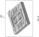
- FIG. 10 schematically illustrates a 3D view of a conventional MEMS mirror device 1000 including comb-type capacitive electrodes 1002 for both of the actuation and the sensing being arranged in a plane with the mirror 1001.
- the conventional MEMS mirrors are based on either planar sensing electrodes located beneath the movable mirror (e.g., device 900 in FIG. 9 ) or the comb-type electrodes arranged in the plane with the mirror (e.g., device 1000 in FIG. 10 ).
- the main advantages of the capacitive sensing are the easy integration of the required electrodes into MEMS processes, and the matureness of the readout electronics that allow resolutions down to the femtofarad (fF) range.
- the conventional MEMS mirrors have the disadvantage that they are not suitable for large tilt angles.
- a large tilt angle requires a correspondingly large gap between the movable mirror plate and the sensing electrodes.
- the measured capacitance is inversely proportional to this spacing.
- the very large electrode areas are needed. Consequently, the large electrodes areas may increase the overall size of the device.
- the comb-type electrodes are applied since they can be relatively compact, e.g., due to the constant small gap between the opposite electrodes. Furthermore, for the low tilt angles a good sensitivity may be achieved. For instance, for the tilt angles, a reproducibility below 0.1° is reported for a range of ⁇ 10°. For the larger tilt angles, the sensitivity may significantly decrease due to the reduced overlap of the electrodes.
- the piezoresistors may be integrated into springs that support the mirror plate. This technologically is by far more complex as the fabrication of electrodes for the capacitive sensing. Another disadvantage is the larger device size. However, a good tilt angle resolution may be obtained.
- FIG. 11 schematically illustrates a conventional MEMS mirror 1100 based on the electromagnetic actuation
- FIG. 12 schematically illustrates a conventional MEMS mirror 1200 based on the piezoresistor placement.
- a minimum detectable angle of approximately 0.002° (30 ⁇ rad) may be measured.
- the reproducibility of the tilt angle may be, for example, as good as 0.001° within a 100 mrad range (about 6°). This rather small tilt angle may be due to the particular applied actuation mechanism.
- a significantly larger ranges may be obtained with the comparable high resolution using piezoelectric sensing.
- the tilt angle may be monitored using an external Position Sensitive Device (PSD), for example, photodiode-based.
- PSD Position Sensitive Device
- an external PSD is typically very expensive.
- an integrated on-chip optical PSD may been used.
- the sound produced by the MEMS mirror may be utilized for the position sensing by applying a microphone as the PSD.
- US 2014/132091 Al discloses a MEMS device.
- the MEMS device applies a magnetic field to the magnetic material, and detects the magnetic field of the magnetic material.
- the present invention is defined by a Micro-Electro-Mechanical-System (MEMS) mirror according to independent claim 1, and a method for determining a position of a moveable mirror according to independent claim 8.
- MEMS Micro-Electro-Mechanical-System
- a first aspect of the invention provides a device, in particular a Micro-Electro-Mechanical-System, MEMS, mirror, comprising a movable structure configured to rotate around at least one axis of rotation; one cylindrical micro-magnet connected to the moveable structure;
- MEMS Micro-Electro-Mechanical-System
- the distance between the micro-magnet and the arrangement of magnetic field sensors may be between 5 ⁇ m to 1000 ⁇ m. In some embodiments, the distance between the micro-magnet and the arrangement of magnetic field sensors may be between 5 ⁇ m and 500 ⁇ m, or between 10 ⁇ m and 100 ⁇ m, etc.
- the device of the first aspect may provide a magnetic sensing (e.g., for the MEMS mirrors), for example, based on a high-flux micro-magnet in combination with an arrangement of the magnetic field sensors.
- the micro-magnet may have a predefined size, volume and structure.
- the micro-magnet is connected to the moveable structure. For example, it may be integrated in the moveable structure, it may be mechanically connected to the moveable structure, fixed to the moveable structure, etc.
- the micro-magnet included in the device may produce a magnetic field.
- the magnetic field produced by the micro-magnet may be sensed by the arrangement of the magnetic field sensors. For example, a direction and/or a magnitude of the magnetic field distribution may be sensed depending on the amount of rotation of the movable axis around the axis of rotation.
- At least two magnetic field sensors from the arrangement of the two or more magnetic field sensors are arranged symmetrically with respect to a default position of the micro-magnet.
- the arrangement of the magnetic field sensors may be such that the at least two magnetic field sensors may be arranged arbitrarily.
- the arrangement may be symmetrical with respect to the micro-magnet.
- the default position of the micro-magnet may be a predefined position, e.g., in which the direction of the magnetic field distribution and/or the magnitude of the magnetic field distribution is known.
- At least two magnetic field sensors from the arrangement of the two or more magnetic field sensors are arranged in a two-dimensional array.
- the arrangement of the two or more magnetic field sensors comprises two or more magnetic elements integrated on one circuit and/or fabricated in parallel on a substrate.
- the circuit is fabricated by a common semiconductor process.
- the integrated micro-magnets may be fabricated in parallel on the wafer level.
- the arrangement of the two or more magnetic field sensors is based on one or more of:
- the magnetic field sensors may be of any known type (Hall, AMR or GMR sensors as well as the MAGFETs). In some embodiments, it may be an array of many single elements integrated on one circuit. In some embodiments, the circuit may be fabricated using a common semiconductor process such as an Atomic Layer Deposition (ALD), a Chemical Vapor Deposition (CVD), a Physical Vapor Deposition (PVD), a Plasma Enhanced Chemical Vapor Deposition (PE-CVD), etc., without limiting the invention to a specific semiconductor process. For example, all sensor elements of the arrangement may be within one plane.
- ALD Atomic Layer Deposition
- CVD Chemical Vapor Deposition
- PVD Physical Vapor Deposition
- PE-CVD Plasma Enhanced Chemical Vapor Deposition
- the movable structure comprises a reflective surface configured to reflect a beam of light.
- a determined angle of rotation of the movable structure around the at least one axis of rotation corresponds to a determined magnetic field distribution sensed by the arrangement of the two or more magnetic field sensors.
- the micro-magnet has a length in the range between 20 ⁇ m and 700 ⁇ m.
- the micro-magnet has a width in the range between 20 ⁇ m and 500 ⁇ m.
- a second aspect of the invention provides a method for determining a position of a moveable structure
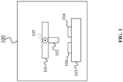
- FIG. 1 schematically illustrates a device 100 according to various embodiments of the invention.
- the device 100 is exemplary based on a MEMS mirror.
- the device 100 comprises a movable structure 101 configured to rotate around at least one axis of rotation 105 indicated by the dotted line, exemplarily into the plane.
- the device 100 further comprises a micro-magnet 102 connected to the moveable structure 101; wherein a rotation of the moveable structure 101 around the at least one axis of rotation 105 rotates the micro-magnet 102 around the same axis of rotation 105.
- the device 100 further comprises a fixed structure 103 comprising an arrangement of two or more magnetic field sensors 104 positioned at a certain distance (h mag ) below the micro-magnet 102, wherein the arrangement of the magnetic field sensors 104 is configured to sense a change of a magnetic field distribution caused by a rotation of the micro-magnet 102.
- the device may be a MEMS mirror, a micro mirror device, etc.
- the micro-magnet may be integrated into the moveable structure.
- the micro-magnet may produce a magnetic field.
- the moveable structure e.g., the integrated micro-magnet to the moveable structure
- the magnetic field distribution may change. The change of the magnetic field distribution may be sensed by the arrangement of the magnetic field sensors, and the position of the moveable structure may be determined.
- FIG. 2 schematically illustrates a device 100 in the form of a MEMS mirror according to various embodiments of the invention.
- the schematic cross-section through the micro mirror 100 illustrates one micro-magnet 102 and an arrangement of the magnetic field sensors 104, which may be used for magnetic position sensing, determining the position of the moveable structure, adjusting the tilt angle, etc.
- the micro-magnet 102 is integrated at the lower side of the movable structure 101 of the micro mirror device 100. Moreover, due to the rigid connection of the micro-magnet 102 to the movable mirror 101, the micro-magnet 102 rotates around the same axis as the moveable mirror, e.g., during the operation and/or the rotation, etc.
- the different component of the device are included in a frame 206.
- the moveable structure 101 of the device 100 comprises a reflective surface (e.g., a moveable mirror plate) configured to reflect a beam of light.
- a reflective surface e.g., a moveable mirror plate
- the change in the position and/or the orientation of the moveable structure 101 may result in a change in the magnetic field seen by the arrangement of the magnetic field sensors 104, for example, the arrangement of the magnetic field sensors 104 may sense the change of the magnetic field distribution caused by the rotation of the micro-magnet 102.
- the magnetic field detected by the arrangement of magnetic field sensors 104 may be utilized, and the position and/or the orientation of the micro-magnet and/or the mirror plate may be tracked.
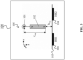
- FIG. 3 schematically illustrates the device 100 in the form of MEMS mirror for sensing magnetic field distribution by an arrangement of two Hall sensors, according to various embodiments of the invention.
- FIG. 3 The exemplary realization of the proposed sensing solution is illustrated in FIG. 3 in which two Hall sensors HS1 and HS2 are utilized in the arrangement of the magnetic field sensors 104.
- the Hall sensors are located in the sensor plane at a distance h mag from the lower end of the micro-magnet 102 in the non-deflected state.
- the distance between the lower end of the micro-magnet 102 and the rotation center of the movable mirror plate 101 (e.g., the moveable structure) is r mag .
- FIG. 4 schematically illustrates the device 100 in the form of MEMS mirror with two axes of rotation 105, according to various embodiments of the invention.
- the device 100 includes a single micro-magnet 102 integrated into the movable structure 101 and four Hall sensors beneath 104
- the arrangement of the magnetic field sensors may be extended, in order to monitor the tilt angle of, for example, the micro-magnet 102 and/or the moveable structure 101 and/or the moveable mirror) included in the micro mirror device 100 in the two independent axis 105.
- two Hall sensors of HS3 and HS4 are placed in the arrangement of the magnetic field sensors.
- the two Hall sensors HS3 and HS4 are further rotated by 90° with respect to the other two sensors (e.g., HS1 and HS2) within the sensor plane, in order to enable measuring in the second axis 405.
- the magnetic field of a cylindrical micro-magnet having a diameter of 50 ⁇ m and with different lengths are simulated, numerically, e.g., based on the arrangement and/or the configuration of the device 100 illustrated in FIG. 3 , without limiting the invention to a specific configuration and/or a specific arrangement of the magnetic field sensors, the micro-magnet, etc.
- FIG. 5 the normalized magnetic flux along the axis of the cylindrical shape (which is parallel to the magnetization direction) is plotted starting at the lower end of the micro-magnet.
- the micro-magnet 102 is considered to be based on an NdFeB magnet, without limiting the invention to a specific micro-magnets.
- FIG. 5 illustrates the simulated normed magnetic flux density (B) as a function of the distance from the lower edge of the micro-magnet with 50 ⁇ m diameter and with various length (L) being fabricated from the NdFeB powder using agglomeration by Atomic Layer Deposition (ALD).
- the volume shaped micro-magnets may be used. Moreover, the effects of using volume shaped micro-magnets may also be derived. For example, in the illustration of the FIG. 5 , it may be derived that the magnetic field strength increases significantly changing the aspect ratio of the cylindrical micro-magnet from 1:1 to 3:1. A further increase may be observed for an aspect ratio of 5:1. However, the benefits may be less.
- micro-magnets with aspect ratio of at least 3:1 may be employed for the proposed sensing solution (e.g., sensing the change of the magnetic field distribution caused by the rotation of the micro-magnet). Producing such a micro-magnets require a thickness which is not achievable by using thin film technologies.
- FIG. 6a schematically illustrate the micro mirror device in the non-titled ground state (e.g., the idle state), according to various embodiments of the invention.
- FIG. 6b illustrate the magnetic field distribution 600 for the micro mirror device 100 in the non-titled ground state, according to various embodiments of the invention.
- the z-component of the magnetic flux (e.g., the magnetic field distribution) is exemplarily illustrated in conjunction with the aforementioned Hall sensors.
- the method for sensing the change of the magnetic field distribution also works for other magnetic field sensors, which may be sensitive to the x- and/or the y-component of the magnetic flux.
- the micro-magnet yields a strongly focused magnetic flux in the sensing plane with a peak values of up to 30 mT.
- the magnetic field is concentrated within a spot of about 100 ⁇ m.
- Hall sensors with a geometrical extend of approximately 100 ⁇ m may be used.
- the two Hall sensors conceived for this exemplary illustration of the sensing concept are placed 100 ⁇ m apart from each other and are indicated by 601 (white lines) in FIG. 6b .
- both sensors see a low magnetic flux with equal magnitudes, in the z direction.
- FIG. 7a schematically illustrate the micro mirror device with a tilt angle of 15°, according to various embodiments of the invention.
- FIG. 7b illustrate the magnetic field distribution 700 for the micro mirror device with a tilt angle of 15°, according to various embodiments of the invention.
- a rotation of 15° of the micro mirror device results in a lateral shift of 107 ⁇ m at the lower end of the micro-magnet.
- This rotation may strongly alter the magnetic field distribution in the sensing plane, as depicted in FIG. 7b .
- the spot of concentrated magnetic flux in z direction may now coincide with the sensing area of HS1, which may lead to a strong asymmetry distribution, in the signals measured by the two sensors.
- the decrease in the peak values of the z-component of the magnetic flux may be, for example, due to the increase in the distance to the sensing plane and the relative tilt (e.g., angle) of the micro-magnet caused by rotation.
- the position of the micro-magnet may be measured from the signals of the Hall sensor in a differential readout scheme.
- the utilization of a differential signal may strongly reduce the impact of the environmental influences, such as the magnetic stray fields or the temperature fluctuations on the accuracy of the sensing the change of the magnetic field distribution and/or determining the position of the moving structure.
- the achievable resolution of sensing the change of the magnetic field distribution and/or determining the position of the moving structure may depends on the performance of the employed magnetic field sensors, the geometry of the utilized micro-magnet, the geometric parameters e.g., the r mag and h mag .
- different magnetic field sensors e.g., the AMR and the GMR sensors may be used.
- the sensor elements may be integrated on the chip-level.
- FIG. 8 shows a method 800 according to an embodiment of the invention for determining a position of a moveable structure 101.
- the method 800 may be carried out by using and/or by means of the device 100, as it described above.
- the method 800 comprises a step 801 of sensing, by an arrangement of two or more magnetic field sensors 104 of a fixed structure 103 positioned at a certain distance (h mag ) below a micro-magnet 102 connected to the moveable structure 101, a change of a magnetic field distribution caused by a rotation of the micro-magnet 102 around at least one axis of rotation 105.
- the method 800 further comprises a step 802 of determining the angle of rotation of the movable structure 101 around the at least one axis of rotation 105 and/or the position of the moveable structure 101, based on the sensed change of the magnetic field distribution.
Landscapes
- Physics & Mathematics (AREA)
- General Physics & Mathematics (AREA)
- Optics & Photonics (AREA)
- Mechanical Light Control Or Optical Switches (AREA)
- Micromachines (AREA)
- Transmission And Conversion Of Sensor Element Output (AREA)
Description
- The present disclosure relates generally to the field of Micro-Electro-Mechanical Systems (MEMS) devices, and more particularly to MEMS mirrors. In this technical filed, the disclosure proposes a device, particularly MEMS mirror, for precise tilting of a movable structure, e.g. mirror, by sensing changes of magnetic field distribution. This disclosure also propose a method for determining a position of a moveable structure by sensing the change of the magnetic field distribution.
- Generally, MEMS devices (also referred to as Micro-Electro-Mechanical, microelectronic and microelectromechanical systems, micro-mechatronics, etc.) are known. Conventional MEMS mirrors are of great interest for a wide range of applications such as imaging devices, optical networks, adaptive light sources, Light Detection and Ranging (LIDAR) applications, material processing, etc. In such MEMS mirrors, it is necessary to monitor the position (e.g., the tilt angle) of the beam steering element (mirror) with high precision. For example, in optical network applications of the MEMS, it is required to control the tilt angle with the highest accuracy. However, in the case of larger angles, as well as for the case of closely packaged MEMS mirror arrays, a robust and low cost technology for precise tilting and monitoring the tilt is not available yet.
- Conventionally, capacitive position sensing is a widely used integrated technique.
FIG. 9 schematically illustrates a cross-section through a conventionalMEMS mirror device 900 utilizing parallel-plate capacitive sensing withfixed electrodes 902 beneath themovable mirror 901 included in afixed frame 903. -
FIG. 10 schematically illustrates a 3D view of a conventionalMEMS mirror device 1000 including comb-typecapacitive electrodes 1002 for both of the actuation and the sensing being arranged in a plane with themirror 1001. - Typically, the conventional MEMS mirrors are based on either planar sensing electrodes located beneath the movable mirror (e.g.,
device 900 inFIG. 9 ) or the comb-type electrodes arranged in the plane with the mirror (e.g.,device 1000 inFIG. 10 ). - The main advantages of the capacitive sensing are the easy integration of the required electrodes into MEMS processes, and the matureness of the readout electronics that allow resolutions down to the femtofarad (fF) range. However, the conventional MEMS mirrors have the disadvantage that they are not suitable for large tilt angles. For example, in the case of the parallel-plate configuration, a large tilt angle requires a correspondingly large gap between the movable mirror plate and the sensing electrodes. The measured capacitance is inversely proportional to this spacing. Moreover, in order to ensure a good sensitivity in the relative readout capacitance of C1/C2, and despite the large gap size, the very large electrode areas are needed. Consequently, the large electrodes areas may increase the overall size of the device.
- Conventionally, the comb-type electrodes are applied since they can be relatively compact, e.g., due to the constant small gap between the opposite electrodes. Furthermore, for the low tilt angles a good sensitivity may be achieved. For instance, for the tilt angles, a reproducibility below 0.1° is reported for a range of ±10°. For the larger tilt angles, the sensitivity may significantly decrease due to the reduced overlap of the electrodes.
- Alternatively, some conventional devices are known that are using the piezoresistive sensing. In such devices, the piezoresistors may be integrated into springs that support the mirror plate. This technologically is by far more complex as the fabrication of electrodes for the capacitive sensing. Another disadvantage is the larger device size. However, a good tilt angle resolution may be obtained.
-
FIG. 11 schematically illustrates aconventional MEMS mirror 1100 based on the electromagnetic actuation, and,FIG. 12 schematically illustrates aconventional MEMS mirror 1200 based on the piezoresistor placement. - In the
conventional MEMS mirror 1100 illustrated inFIG. 11 , four wheatstone bridges with sixteen piezoresistors are required, in total, in order to ensure a full in-plane control with the high sensitivity. - Moreover, a minimum detectable angle of approximately 0.002° (30 µrad) may be measured. The reproducibility of the tilt angle may be, for example, as good as 0.001° within a 100 mrad range (about 6°). This rather small tilt angle may be due to the particular applied actuation mechanism. In addition, a significantly larger ranges may be obtained with the comparable high resolution using piezoelectric sensing.
- In addition, apart from the described techniques, the tilt angle may be monitored using an external Position Sensitive Device (PSD), for example, photodiode-based. Furthermore, for applications that require large mirror arrays, using an external PSD is typically very expensive. In order to overcome this restrain, an integrated on-chip optical PSD may been used. Alternatively, the sound produced by the MEMS mirror may be utilized for the position sensing by applying a microphone as the PSD.
- Conventional devices (on the scale of mm to m) are known that use magnetic position sensing. For example, the magnetic principles are known to be applied for e.g., various actuators, MEMS resonators, and tactile sensors, etc. Magnetic position sensing provides several advantages, for example, it is precise, cheaper than the optical sensing, and is insensitive to contaminations. However, the conventional devices have several drawbacks due to, for example, the lack of suitable micro-magnets (e.g., since magnetic forces scale with the volume, larger magnets are advantageous which cannot be easily produced). The traditional sintering techniques are suitable only for larger magnets and not for the micro-magnets. The common deposition processes of semiconductor technology provide only thin layers and the volume of obtained magnets may be very low. Moreover, the integration of the micro-magnets on planar substrates is not known.
- AND NANOPHOTONICS (OMN), IEEE, 18 August 2013 (2013-08-18), pages 99-100, discloses a 2D MEMS scanner with a rotation-angle detector for a time-of-flight image sensor.
-
US 2014/132091 Al discloses a MEMS device. The MEMS device applies a magnetic field to the magnetic material, and detects the magnetic field of the magnetic material. - The objective of the present invention is achieved by the solution provided in the enclosed independent claims. Advantageous implementations of the present invention are further defined in the dependent claims.
- The present invention is defined by a Micro-Electro-Mechanical-System (MEMS) mirror according to
independent claim 1, and a method for determining a position of a moveable mirror according to independent claim 8. - A first aspect of the invention, as defined by
claim 1, provides a device, in particular a Micro-Electro-Mechanical-System, MEMS, mirror, comprising a movable structure configured to rotate around at least one axis of rotation; one cylindrical micro-magnet connected to the moveable structure; - wherein a rotation of the moveable structure around the at least one axis of rotation rotates the micro-magnet around the same axis of rotation; and a fixed structure comprising an arrangement of two or more magnetic field sensors positioned at a certain distance below the micro-magnet,
- wherein the distance between the fixed structure and the micro-magnet is in the range between 5 µm to 1000 µm,
- wherein the arrangement of the magnetic field sensors is configured to sense a change of a magnetic field distribution caused by a rotation of the micro-magnet.
- For example, in some embodiments, the distance between the micro-magnet and the arrangement of magnetic field sensors may be between 5 µm to 1000 µm. In some embodiments, the distance between the micro-magnet and the arrangement of magnetic field sensors may be between 5 µm and 500 µm, or between 10 µm and 100 µm, etc.
- The device of the first aspect may provide a magnetic sensing (e.g., for the MEMS mirrors), for example, based on a high-flux micro-magnet in combination with an arrangement of the magnetic field sensors.
- The micro-magnet may have a predefined size, volume and structure. The micro-magnet is connected to the moveable structure. For example, it may be integrated in the moveable structure, it may be mechanically connected to the moveable structure, fixed to the moveable structure, etc. Moreover, the micro-magnet included in the device may produce a magnetic field. The magnetic field produced by the micro-magnet may be sensed by the arrangement of the magnetic field sensors. For example, a direction and/or a magnitude of the magnetic field distribution may be sensed depending on the amount of rotation of the movable axis around the axis of rotation.
- In an implementation form of the first aspect, at least two magnetic field sensors from the arrangement of the two or more magnetic field sensors are arranged symmetrically with respect to a default position of the micro-magnet.
- For example, in some embodiments, the arrangement of the magnetic field sensors may be such that the at least two magnetic field sensors may be arranged arbitrarily. For instance, the arrangement may be symmetrical with respect to the micro-magnet. The default position of the micro-magnet may be a predefined position, e.g., in which the direction of the magnetic field distribution and/or the magnitude of the magnetic field distribution is known.
- In a further implementation form of the first aspect, at least two magnetic field sensors from the arrangement of the two or more magnetic field sensors are arranged in a two-dimensional array.
- In a further implementation form of the first aspect, the arrangement of the two or more magnetic field sensors comprises two or more magnetic elements integrated on one circuit and/or fabricated in parallel on a substrate.
- In a further implementation form of the first aspect, the circuit is fabricated by a common semiconductor process.
- For example, the integrated micro-magnets may be fabricated in parallel on the wafer level.
- In a further implementation form of the first aspect, the arrangement of the two or more magnetic field sensors is based on one or more of:
- A Hall sensor.
- An Anisotropic Magneto-Resistive, AMR, magnetic sensor.
- A Giant Magnetoresistance, GMR, sensor.
- A Magnetic Field-Effect Transistor, MAGFET, sensor.
- For example, the magnetic field sensors may be of any known type (Hall, AMR or GMR sensors as well as the MAGFETs). In some embodiments, it may be an array of many single elements integrated on one circuit. In some embodiments, the circuit may be fabricated using a common semiconductor process such as an Atomic Layer Deposition (ALD), a Chemical Vapor Deposition (CVD), a Physical Vapor Deposition (PVD), a Plasma Enhanced Chemical Vapor Deposition (PE-CVD), etc., without limiting the invention to a specific semiconductor process. For example, all sensor elements of the arrangement may be within one plane.
- In a further implementation form of the first aspect, the movable structure comprises a reflective surface configured to reflect a beam of light.
- In a further implementation form of the first aspect, a determined angle of rotation of the movable structure around the at least one axis of rotation corresponds to a determined magnetic field distribution sensed by the arrangement of the two or more magnetic field sensors.
- In a further implementation form of the first aspect, the micro-magnet has a length in the range between 20 µm and 700 µm.
- In a further implementation form of the first aspect, the micro-magnet has a width in the range between 20 µm and 500 µm.
- A second aspect of the invention provides a method for determining a position of a moveable structure
- In an implementation form of the third aspect the method comprises sensing, by an arrangement of two or more magnetic field sensors of a fixed structure positioned at a certain distance (hmag) below a micro-magnet connected to the moveable structure, a change of a magnetic field distribution caused by a rotation of the micro-magnet around at least one axis of rotation, wherein the cylindrical micro-magnet has an aspect ratio larger than 1:1, and wherein the distance (hmag) between the fixed structure and the micro-magnet is in the range between 5 µm to 1000 µm; and
- In an implementation form of the third aspect the method determines the angle of rotation of the movable structure around the at least one axis of rotation and/or the position of the moveable structure, based on the sensed change of the magnetic field distribution.
- It has to be noted that all devices, elements, units and means described in the present application could be implemented in the software or hardware elements or any kind of combination thereof. All steps which are performed by the various entities described in the present application as well as the functionalities described to be performed by the various entities are intended to mean that the respective entity is adapted to or configured to perform the respective steps and functionalities. Even if, in the following description of specific embodiments, a specific functionality or step to be performed by external entities is not reflected in the description of a specific detailed element of that entity which performs that specific step or functionality, it should be clear for a skilled person that these methods and functionalities can be implemented in respective software or hardware elements, or any kind of combination thereof.
- The above described aspects and implementation forms of the present invention will be explained in the following description of specific embodiments in relation to the enclosed drawings, in which
- FIG. 1
- schematically illustrates a device, according to various embodiments of the invention.
- FIG. 2
- schematically illustrates the device in a form of a Micro-Electro-Mechanical-System mirror, according to various embodiments of the invention.
- FIG. 3
- schematically illustrates the device in the form of MEMS mirror for sensing magnetic field distribution by an arrangement of two Hall sensors, according to various embodiments of the invention.
- FIG. 4
- schematically illustrates the device in the form of MEMS mirror with two axes of rotation, according to various embodiments of the invention.
- FIG. 5
- illustrates simulated magnetic flux density as a function of the distance from the lower edge of the micro-magnet of the device, according to various embodiments of the invention.
- FIG. 6a
- schematically illustrate the micro mirror device in the non-titled ground state, and
FIG. 6b illustrate the magnetic field distribution for the micro mirror device in the non-titled ground state, according to various embodiments of the invention. - FIG. 7a
- schematically illustrate the micro mirror device with a tilt angle of 15°, and
FIG. 7b illustrate the magnetic field distribution for the micro mirror device with a tilt angle of 15°, according to various embodiments of the invention. - FIG. 8
- schematically illustrates a method for determining a position of a moveable structure, according to various embodiments of the invention.
- FIG. 9
- schematically illustrates a conventional mirror device based on the parallel-plate capacitive sensing, according to the prior art.
- FIG. 10
- schematically illustrates a 3D view of a conventional MEMS mirror device including comb-type capacitive electrodes, according to the prior art.
- FIG. 11
- schematically illustrates a conventional MEMS mirror based on the electromagnetic actuation, according to the prior art.
- FIG. 12
- schematically illustrates a conventional MEMS mirror based on the piezoresistor placement, according to the prior art.
-
FIG. 1 schematically illustrates adevice 100 according to various embodiments of the invention. - The
device 100 is exemplary based on a MEMS mirror. Thedevice 100 comprises amovable structure 101 configured to rotate around at least one axis ofrotation 105 indicated by the dotted line, exemplarily into the plane. - The
device 100 further comprises a micro-magnet 102 connected to themoveable structure 101; wherein a rotation of themoveable structure 101 around the at least one axis ofrotation 105 rotates the micro-magnet 102 around the same axis ofrotation 105. - The
device 100 further comprises a fixedstructure 103 comprising an arrangement of two or moremagnetic field sensors 104 positioned at a certain distance (hmag) below the micro-magnet 102, wherein the arrangement of themagnetic field sensors 104 is configured to sense a change of a magnetic field distribution caused by a rotation of the micro-magnet 102. - The device may be a MEMS mirror, a micro mirror device, etc. In some embodiments, the micro-magnet may be integrated into the moveable structure. The micro-magnet may produce a magnetic field. Moreover, when the moveable structure (e.g., the integrated micro-magnet to the moveable structure) rotates, the magnetic field distribution may change. The change of the magnetic field distribution may be sensed by the arrangement of the magnetic field sensors, and the position of the moveable structure may be determined.
-
FIG. 2 schematically illustrates adevice 100 in the form of a MEMS mirror according to various embodiments of the invention. - The schematic cross-section through the
micro mirror 100 illustrates onemicro-magnet 102 and an arrangement of themagnetic field sensors 104, which may be used for magnetic position sensing, determining the position of the moveable structure, adjusting the tilt angle, etc. - In the
device 100 of theFIG. 2 , the micro-magnet 102 is integrated at the lower side of themovable structure 101 of themicro mirror device 100. Moreover, due to the rigid connection of the micro-magnet 102 to themovable mirror 101, the micro-magnet 102 rotates around the same axis as the moveable mirror, e.g., during the operation and/or the rotation, etc. The different component of the device are included in aframe 206. - The
moveable structure 101 of thedevice 100 comprises a reflective surface (e.g., a moveable mirror plate) configured to reflect a beam of light. - In addition, the change in the position and/or the orientation of the moveable structure 101 (e.g., the mirror plate) may result in a change in the magnetic field seen by the arrangement of the
magnetic field sensors 104, for example, the arrangement of themagnetic field sensors 104 may sense the change of the magnetic field distribution caused by the rotation of the micro-magnet 102. - Furthermore, the magnetic field detected by the arrangement of
magnetic field sensors 104 may be utilized, and the position and/or the orientation of the micro-magnet and/or the mirror plate may be tracked. -
FIG. 3 schematically illustrates thedevice 100 in the form of MEMS mirror for sensing magnetic field distribution by an arrangement of two Hall sensors, according to various embodiments of the invention. - The exemplary realization of the proposed sensing solution is illustrated in
FIG. 3 in which two Hall sensors HS1 and HS2 are utilized in the arrangement of themagnetic field sensors 104. The Hall sensors are located in the sensor plane at a distance hmag from the lower end of the micro-magnet 102 in the non-deflected state. Moreover, the distance between the lower end of the micro-magnet 102 and the rotation center of the movable mirror plate 101 (e.g., the moveable structure) is rmag. -
FIG. 4 schematically illustrates thedevice 100 in the form of MEMS mirror with two axes ofrotation 105, according to various embodiments of the invention. Thedevice 100 includes asingle micro-magnet 102 integrated into themovable structure 101 and four Hall sensors beneath 104 - The arrangement of the magnetic field sensors (e.g., as it is illustrated in the embodiment of the
FIG. 3 ) may be extended, in order to monitor the tilt angle of, for example, the micro-magnet 102 and/or themoveable structure 101 and/or the moveable mirror) included in themicro mirror device 100 in the twoindependent axis 105. - In addition, two Hall sensors of HS3 and HS4, are placed in the arrangement of the magnetic field sensors. The two Hall sensors HS3 and HS4 are further rotated by 90° with respect to the other two sensors (e.g., HS1 and HS2) within the sensor plane, in order to enable measuring in the
second axis 405. - In the following, in order to estimate the performance of the proposed sensing solution (i.e., the change of the magnetic field distribution caused by the rotation of the micro-magnet), the magnetic field of a cylindrical micro-magnet having a diameter of 50 µm and with different lengths are simulated, numerically, e.g., based on the arrangement and/or the configuration of the
device 100 illustrated inFIG. 3 , without limiting the invention to a specific configuration and/or a specific arrangement of the magnetic field sensors, the micro-magnet, etc. - In
FIG. 5 the normalized magnetic flux along the axis of the cylindrical shape (which is parallel to the magnetization direction) is plotted starting at the lower end of the micro-magnet. The micro-magnet 102 is considered to be based on an NdFeB magnet, without limiting the invention to a specific micro-magnets. -
FIG. 5 illustrates the simulated normed magnetic flux density (B) as a function of the distance from the lower edge of the micro-magnet with 50 µm diameter and with various length (L) being fabricated from the NdFeB powder using agglomeration by Atomic Layer Deposition (ALD). - As can be derived from
FIG. 5 , even the smallest powder-based NdFeB magnets generate a considerable magnetic field over tens of microns distance. The generated magnetic field is sufficient for the detection with the Hall sensors. - In some embodiments, the volume shaped micro-magnets may be used. Moreover, the effects of using volume shaped micro-magnets may also be derived. For example, in the illustration of the
FIG. 5 , it may be derived that the magnetic field strength increases significantly changing the aspect ratio of the cylindrical micro-magnet from 1:1 to 3:1. A further increase may be observed for an aspect ratio of 5:1. However, the benefits may be less. In some embodiments, micro-magnets with aspect ratio of at least 3:1 may be employed for the proposed sensing solution (e.g., sensing the change of the magnetic field distribution caused by the rotation of the micro-magnet). Producing such a micro-magnets require a thickness which is not achievable by using thin film technologies. - In the following, a cylindrical micro-magnet with diameter of 50 µm and an aspect ratio of 5:1 is considered, as an exemplary illustration of sensing the change of the magnetic field distribution.
FIGs. 6a, 6b ,7b and 7b illustrate the magnetic field distribution in the sensing plane at the distance of hmag= 50 µm for different tilt angles. -
FIG. 6a schematically illustrate the micro mirror device in the non-titled ground state (e.g., the idle state), according to various embodiments of the invention.FIG. 6b illustrate themagnetic field distribution 600 for themicro mirror device 100 in the non-titled ground state, according to various embodiments of the invention. - The z-component of the magnetic flux (e.g., the magnetic field distribution) is exemplarily illustrated in conjunction with the aforementioned Hall sensors. The method for sensing the change of the magnetic field distribution also works for other magnetic field sensors, which may be sensitive to the x- and/or the y-component of the magnetic flux.
- As can be derived from the
FIG. 6b , the micro-magnet yields a strongly focused magnetic flux in the sensing plane with a peak values of up to 30 mT. The magnetic field is concentrated within a spot of about 100 µm. In some embodiments, Hall sensors with a geometrical extend of approximately 100 µm may be used. Moreover, the two Hall sensors conceived for this exemplary illustration of the sensing concept are placed 100 µm apart from each other and are indicated by 601 (white lines) inFIG. 6b . In the non-titled ground state of the micro mirror device (illustrated inFIG. 6a and FIG. 6b ), both sensors see a low magnetic flux with equal magnitudes, in the z direction. -
FIG. 7a schematically illustrate the micro mirror device with a tilt angle of 15°, according to various embodiments of the invention.FIG. 7b illustrate themagnetic field distribution 700 for the micro mirror device with a tilt angle of 15°, according to various embodiments of the invention. - For a center of rotation positioned at a distance of rmag = 400 µm from the lower end of the micro-magnet, a rotation of 15° of the micro mirror device (and thus the micro-magnet) results in a lateral shift of 107 µm at the lower end of the micro-magnet. This rotation may strongly alter the magnetic field distribution in the sensing plane, as depicted in
FIG. 7b . The spot of concentrated magnetic flux in z direction may now coincide with the sensing area of HS1, which may lead to a strong asymmetry distribution, in the signals measured by the two sensors. The decrease in the peak values of the z-component of the magnetic flux may be, for example, due to the increase in the distance to the sensing plane and the relative tilt (e.g., angle) of the micro-magnet caused by rotation. - In some embodiments, the position of the micro-magnet may be measured from the signals of the Hall sensor in a differential readout scheme. For example, the utilization of a differential signal may strongly reduce the impact of the environmental influences, such as the magnetic stray fields or the temperature fluctuations on the accuracy of the sensing the change of the magnetic field distribution and/or determining the position of the moving structure.
- In some embodiments, the achievable resolution of sensing the change of the magnetic field distribution and/or determining the position of the moving structure may depends on the performance of the employed magnetic field sensors, the geometry of the utilized micro-magnet, the geometric parameters e.g., the rmag and hmag.
- In some embodiments, different magnetic field sensors, e.g., the AMR and the GMR sensors may be used. Moreover, the sensor elements may be integrated on the chip-level.
-
FIG. 8 shows amethod 800 according to an embodiment of the invention for determining a position of amoveable structure 101. Themethod 800 may be carried out by using and/or by means of thedevice 100, as it described above. - The
method 800 comprises astep 801 of sensing, by an arrangement of two or moremagnetic field sensors 104 of a fixedstructure 103 positioned at a certain distance (hmag) below a micro-magnet 102 connected to themoveable structure 101, a change of a magnetic field distribution caused by a rotation of the micro-magnet 102 around at least one axis ofrotation 105. - The
method 800 further comprises astep 802 of determining the angle of rotation of themovable structure 101 around the at least one axis ofrotation 105 and/or the position of themoveable structure 101, based on the sensed change of the magnetic field distribution. - Embodiments of the present invention have been described in conjunction with various embodiments as examples as well as implementations. However, other variations can be understood and effected by those persons skilled in the art and practicing the claimed invention, from the studies of the drawings, this disclosure and the independent claims. In the claims as well as in the description the word "comprising" does not exclude other elements or steps and the indefinite article "a" or "an" does not exclude a plurality. A single element or other unit may fulfill the functions of several entities or items recited in the claims. The mere fact that certain measures are recited in the mutual different dependent claims does not indicate that a combination of these measures cannot be used in an advantageous implementation.
Claims (8)
- Device (100), in particular a Micro-Electro-Mechanical-System, MEMS, mirror, comprising:a movable structure (101) configured to rotate around at least one axis of rotation (105);one micro-magnet (102) connected to the moveable structure (101), wherein the micro-magnet (102) is cylindrical and has an aspect ratio larger than 1:1;wherein a rotation of the moveable structure (101) around the at least one axis of rotation (105) rotates the micro-magnet (102) around the same axis of rotation (105); anda fixed structure (103) comprising an arrangement of two or more magnetic field sensors (104) positioned at a certain distance (hmag) below the micro-magnet (102), wherein the distance (hmag) between the fixed structure (103) and the micro-magnet (102) is in the range between 5 µm to 1000 µm,wherein the arrangement of the magnetic field sensors (104) is configured to sense a change of a magnetic field distribution caused by a rotation of the micro-magnet (102).
- Device (100) according to claim 1, wherein
at least two magnetic field sensors from the arrangement of the two or more magnetic field sensors (104) are arranged symmetrically with respect to a default position of the micro-magnet (101). - Device (100) according to claim 1 or 2, wherein
at least two magnetic field sensors from the arrangement of the two or more magnetic field sensors (104) are arranged in a two-dimensional array. - Device (100) according to any one of claims 1 to 3, wherein
the arrangement of the two or more magnetic field sensors comprises two or more magnetic elements (104) integrated on one circuit and/or fabricated in parallel on a substrate. - Device (100) according to any one of claims 1 to 4, wherein
the arrangement of the two or more magnetic field sensors (104) is based on one or more of:- a Hall sensor,- an Anisotropic Magneto-Resistive, AMR, magnetic sensor,- a Giant Magnetoresistance, GMR, sensor,- a Magnetic Field-Effect Transistor, MAGFET, sensor. - Device (100) according to any one of claims 1 to 5, wherein
the movable structure (101) comprises a reflective surface configured to reflect a beam of light. - Device (100) according to any one of claims 1 to 6, wherein
a determined angle of rotation of the movable structure (101) around the at least one axis of rotation (105) corresponds to a determined magnetic field distribution sensed by the arrangement of the two or more magnetic field sensors (104). - Method (800) for determining a position of a moveable structure (101), the method (800) comprising:sensing (801), by an arrangement of two or more magnetic field sensors (104) of a fixed structure (103) positioned at a certain distance (hmag) below a micro-magnet (102) connected to the moveable structure (101), a change of a magnetic field distribution caused by a rotation of the micro-magnet (102) around at least one axis of rotation (105), wherein the micro-magnet (102) is cylindrical and has an aspect ratio larger than 1:1; and wherein the distance (hmag) between the fixed structure (103) and the micro-magnet (102) is in the range between 5 µm to 1000 µm; anddetermining (802) the angle of rotation of the movable structure (101) around the at least one axis of rotation (105) and/or the position of the moveable structure (101), based on the sensed change of the magnetic field distribution.
Applications Claiming Priority (1)
| Application Number | Priority Date | Filing Date | Title |
|---|---|---|---|
| PCT/EP2019/053319 WO2020164684A1 (en) | 2019-02-11 | 2019-02-11 | Device and method for sensing magnetic field distribution |
Publications (2)
| Publication Number | Publication Date |
|---|---|
| EP3899635A1 EP3899635A1 (en) | 2021-10-27 |
| EP3899635B1 true EP3899635B1 (en) | 2025-04-23 |
Family
ID=65443829
Family Applications (1)
| Application Number | Title | Priority Date | Filing Date |
|---|---|---|---|
| EP19705721.9A Active EP3899635B1 (en) | 2019-02-11 | 2019-02-11 | Device and method for sensing magnetic field distribution |
Country Status (2)
| Country | Link |
|---|---|
| EP (1) | EP3899635B1 (en) |
| WO (1) | WO2020164684A1 (en) |
Family Cites Families (4)
| Publication number | Priority date | Publication date | Assignee | Title |
|---|---|---|---|---|
| JP2657769B2 (en) * | 1994-01-31 | 1997-09-24 | 正喜 江刺 | Planar type galvanometer mirror having displacement detection function and method of manufacturing the same |
| JP4380233B2 (en) * | 2002-10-18 | 2009-12-09 | 日本ビクター株式会社 | Optical deflector |
| JP5708115B2 (en) * | 2011-03-24 | 2015-04-30 | 株式会社豊田中央研究所 | Optical deflection device |
| JP5768803B2 (en) * | 2012-11-15 | 2015-08-26 | 株式会社豊田中央研究所 | MEMS equipment |
-
2019
- 2019-02-11 EP EP19705721.9A patent/EP3899635B1/en active Active
- 2019-02-11 WO PCT/EP2019/053319 patent/WO2020164684A1/en not_active Ceased
Also Published As
| Publication number | Publication date |
|---|---|
| EP3899635A1 (en) | 2021-10-27 |
| WO2020164684A1 (en) | 2020-08-20 |
Similar Documents
| Publication | Publication Date | Title |
|---|---|---|
| EP3954972B1 (en) | Magnetoresistive inertial sensor chip | |
| US6507187B1 (en) | Ultra-sensitive magnetoresistive displacement sensing device | |
| CN114667266B (en) | Microsystem and production method thereof | |
| CN109941956B (en) | MEMS sensor and electronic equipment | |
| US7453269B2 (en) | Magnetic MEMS sensor device | |
| CN103323795B (en) | Integrated three-axis magnetic sensor | |
| EP2257821B1 (en) | Capacitive sensor having cyclic and absolute electrode sets | |
| US7583081B2 (en) | Magnetostrictive multi-layer sensor for detecting a deformation | |
| US7492554B2 (en) | Magnetic sensor with tilted magnetoresistive structures | |
| CN103116144B (en) | Z-direction magnetic field sensor with magnetic orbit structure | |
| CN101065721A (en) | Magnetic sensor for input devices | |
| JPH1151967A (en) | Multi-axis acceleration sensor and manufacturing method thereof | |
| EP2339362A1 (en) | Magnetic sensor module and piston position detector | |
| CN107356249A (en) | A kind of micro- inertia component of tunnel magnetoresistive detection | |
| CN107421525A (en) | A kind of tunnel magnetoresistive disresonance type 3 axis MEMS gyro | |
| JP2003294545A (en) | Force detection device | |
| CN110345972B (en) | Sensor and electronic equipment | |
| EP1521071B1 (en) | Dynamometrical sensor device, manufacturing process and detection system therefrom | |
| CN112014778B (en) | Magneto-resistive sensor of micro-electromechanical system, sensor unit and electronic equipment | |
| CN207395752U (en) | A kind of micro- inertia component of tunnel magnetoresistive detection | |
| WO2020164684A1 (en) | Device and method for sensing magnetic field distribution | |
| Fuji et al. | Spin-MEMS microphone integrating a series of magnetic tunnel junctions on a rectangular diaphragm | |
| CN112305471A (en) | Magnetic field sensor, system and oblique incidence deposition manufacturing method | |
| CN110207586B (en) | Layout structure of magnetoresistance in a magnetic sensor chip and magnetic sensor chip | |
| JPS6311672Y2 (en) |
Legal Events
| Date | Code | Title | Description |
|---|---|---|---|
| STAA | Information on the status of an ep patent application or granted ep patent |
Free format text: STATUS: UNKNOWN |
|
| STAA | Information on the status of an ep patent application or granted ep patent |
Free format text: STATUS: THE INTERNATIONAL PUBLICATION HAS BEEN MADE |
|
| PUAI | Public reference made under article 153(3) epc to a published international application that has entered the european phase |
Free format text: ORIGINAL CODE: 0009012 |
|
| STAA | Information on the status of an ep patent application or granted ep patent |
Free format text: STATUS: REQUEST FOR EXAMINATION WAS MADE |
|
| 17P | Request for examination filed |
Effective date: 20210722 |
|
| AK | Designated contracting states |
Kind code of ref document: A1 Designated state(s): AL AT BE BG CH CY CZ DE DK EE ES FI FR GB GR HR HU IE IS IT LI LT LU LV MC MK MT NL NO PL PT RO RS SE SI SK SM TR |
|
| RAP3 | Party data changed (applicant data changed or rights of an application transferred) |
Owner name: FRAUNHOFER-GESELLSCHAFT ZUR FOERDERUNG DER ANGEWANDTEN FORSCHUNG E.V. Owner name: HUAWEI TECHNOLOGIES CO., LTD. |
|
| DAV | Request for validation of the european patent (deleted) | ||
| DAX | Request for extension of the european patent (deleted) | ||
| STAA | Information on the status of an ep patent application or granted ep patent |
Free format text: STATUS: EXAMINATION IS IN PROGRESS |
|
| 17Q | First examination report despatched |
Effective date: 20230809 |
|
| GRAP | Despatch of communication of intention to grant a patent |
Free format text: ORIGINAL CODE: EPIDOSNIGR1 |
|
| STAA | Information on the status of an ep patent application or granted ep patent |
Free format text: STATUS: GRANT OF PATENT IS INTENDED |
|
| INTG | Intention to grant announced |
Effective date: 20241210 |
|
| GRAS | Grant fee paid |
Free format text: ORIGINAL CODE: EPIDOSNIGR3 |
|
| GRAA | (expected) grant |
Free format text: ORIGINAL CODE: 0009210 |
|
| STAA | Information on the status of an ep patent application or granted ep patent |
Free format text: STATUS: THE PATENT HAS BEEN GRANTED |
|
| AK | Designated contracting states |
Kind code of ref document: B1 Designated state(s): AL AT BE BG CH CY CZ DE DK EE ES FI FR GB GR HR HU IE IS IT LI LT LU LV MC MK MT NL NO PL PT RO RS SE SI SK SM TR |
|
| REG | Reference to a national code |
Ref country code: GB Ref legal event code: FG4D |
|
| REG | Reference to a national code |
Ref country code: CH Ref legal event code: EP |
|
| REG | Reference to a national code |
Ref country code: DE Ref legal event code: R096 Ref document number: 602019068959 Country of ref document: DE |
|
| REG | Reference to a national code |
Ref country code: IE Ref legal event code: FG4D |
|
| REG | Reference to a national code |
Ref country code: NL Ref legal event code: MP Effective date: 20250423 |
|
| PG25 | Lapsed in a contracting state [announced via postgrant information from national office to epo] |
Ref country code: NL Free format text: LAPSE BECAUSE OF FAILURE TO SUBMIT A TRANSLATION OF THE DESCRIPTION OR TO PAY THE FEE WITHIN THE PRESCRIBED TIME-LIMIT Effective date: 20250423 |
|
| REG | Reference to a national code |
Ref country code: AT Ref legal event code: MK05 Ref document number: 1788287 Country of ref document: AT Kind code of ref document: T Effective date: 20250423 |
|
| PG25 | Lapsed in a contracting state [announced via postgrant information from national office to epo] |
Ref country code: PT Free format text: LAPSE BECAUSE OF FAILURE TO SUBMIT A TRANSLATION OF THE DESCRIPTION OR TO PAY THE FEE WITHIN THE PRESCRIBED TIME-LIMIT Effective date: 20250825 Ref country code: FI Free format text: LAPSE BECAUSE OF FAILURE TO SUBMIT A TRANSLATION OF THE DESCRIPTION OR TO PAY THE FEE WITHIN THE PRESCRIBED TIME-LIMIT Effective date: 20250423 Ref country code: ES Free format text: LAPSE BECAUSE OF FAILURE TO SUBMIT A TRANSLATION OF THE DESCRIPTION OR TO PAY THE FEE WITHIN THE PRESCRIBED TIME-LIMIT Effective date: 20250423 |
|
| REG | Reference to a national code |
Ref country code: LT Ref legal event code: MG9D |
|
| PG25 | Lapsed in a contracting state [announced via postgrant information from national office to epo] |
Ref country code: NO Free format text: LAPSE BECAUSE OF FAILURE TO SUBMIT A TRANSLATION OF THE DESCRIPTION OR TO PAY THE FEE WITHIN THE PRESCRIBED TIME-LIMIT Effective date: 20250723 Ref country code: GR Free format text: LAPSE BECAUSE OF FAILURE TO SUBMIT A TRANSLATION OF THE DESCRIPTION OR TO PAY THE FEE WITHIN THE PRESCRIBED TIME-LIMIT Effective date: 20250724 |
|
| PG25 | Lapsed in a contracting state [announced via postgrant information from national office to epo] |
Ref country code: PL Free format text: LAPSE BECAUSE OF FAILURE TO SUBMIT A TRANSLATION OF THE DESCRIPTION OR TO PAY THE FEE WITHIN THE PRESCRIBED TIME-LIMIT Effective date: 20250423 |
|
| PG25 | Lapsed in a contracting state [announced via postgrant information from national office to epo] |
Ref country code: BG Free format text: LAPSE BECAUSE OF FAILURE TO SUBMIT A TRANSLATION OF THE DESCRIPTION OR TO PAY THE FEE WITHIN THE PRESCRIBED TIME-LIMIT Effective date: 20250423 |
|
| PG25 | Lapsed in a contracting state [announced via postgrant information from national office to epo] |
Ref country code: HR Free format text: LAPSE BECAUSE OF FAILURE TO SUBMIT A TRANSLATION OF THE DESCRIPTION OR TO PAY THE FEE WITHIN THE PRESCRIBED TIME-LIMIT Effective date: 20250423 |
|
| PG25 | Lapsed in a contracting state [announced via postgrant information from national office to epo] |
Ref country code: AT Free format text: LAPSE BECAUSE OF FAILURE TO SUBMIT A TRANSLATION OF THE DESCRIPTION OR TO PAY THE FEE WITHIN THE PRESCRIBED TIME-LIMIT Effective date: 20250423 |
|
| PG25 | Lapsed in a contracting state [announced via postgrant information from national office to epo] |
Ref country code: RS Free format text: LAPSE BECAUSE OF FAILURE TO SUBMIT A TRANSLATION OF THE DESCRIPTION OR TO PAY THE FEE WITHIN THE PRESCRIBED TIME-LIMIT Effective date: 20250723 |
|
| PG25 | Lapsed in a contracting state [announced via postgrant information from national office to epo] |
Ref country code: IS Free format text: LAPSE BECAUSE OF FAILURE TO SUBMIT A TRANSLATION OF THE DESCRIPTION OR TO PAY THE FEE WITHIN THE PRESCRIBED TIME-LIMIT Effective date: 20250823 |
|
| PG25 | Lapsed in a contracting state [announced via postgrant information from national office to epo] |
Ref country code: LV Free format text: LAPSE BECAUSE OF FAILURE TO SUBMIT A TRANSLATION OF THE DESCRIPTION OR TO PAY THE FEE WITHIN THE PRESCRIBED TIME-LIMIT Effective date: 20250423 |
|
| PG25 | Lapsed in a contracting state [announced via postgrant information from national office to epo] |
Ref country code: DK Free format text: LAPSE BECAUSE OF FAILURE TO SUBMIT A TRANSLATION OF THE DESCRIPTION OR TO PAY THE FEE WITHIN THE PRESCRIBED TIME-LIMIT Effective date: 20250423 Ref country code: SM Free format text: LAPSE BECAUSE OF FAILURE TO SUBMIT A TRANSLATION OF THE DESCRIPTION OR TO PAY THE FEE WITHIN THE PRESCRIBED TIME-LIMIT Effective date: 20250423 |
|
| PG25 | Lapsed in a contracting state [announced via postgrant information from national office to epo] |
Ref country code: CZ Free format text: LAPSE BECAUSE OF FAILURE TO SUBMIT A TRANSLATION OF THE DESCRIPTION OR TO PAY THE FEE WITHIN THE PRESCRIBED TIME-LIMIT Effective date: 20250423 |
|
| PG25 | Lapsed in a contracting state [announced via postgrant information from national office to epo] |
Ref country code: EE Free format text: LAPSE BECAUSE OF FAILURE TO SUBMIT A TRANSLATION OF THE DESCRIPTION OR TO PAY THE FEE WITHIN THE PRESCRIBED TIME-LIMIT Effective date: 20250423 |
|
| REG | Reference to a national code |
Ref country code: DE Ref legal event code: R097 Ref document number: 602019068959 Country of ref document: DE |
|
| PG25 | Lapsed in a contracting state [announced via postgrant information from national office to epo] |
Ref country code: SK Free format text: LAPSE BECAUSE OF FAILURE TO SUBMIT A TRANSLATION OF THE DESCRIPTION OR TO PAY THE FEE WITHIN THE PRESCRIBED TIME-LIMIT Effective date: 20250423 Ref country code: RO Free format text: LAPSE BECAUSE OF FAILURE TO SUBMIT A TRANSLATION OF THE DESCRIPTION OR TO PAY THE FEE WITHIN THE PRESCRIBED TIME-LIMIT Effective date: 20250423 |
|
| PG25 | Lapsed in a contracting state [announced via postgrant information from national office to epo] |
Ref country code: IT Free format text: LAPSE BECAUSE OF FAILURE TO SUBMIT A TRANSLATION OF THE DESCRIPTION OR TO PAY THE FEE WITHIN THE PRESCRIBED TIME-LIMIT Effective date: 20250423 |
|
| PLBE | No opposition filed within time limit |
Free format text: ORIGINAL CODE: 0009261 |
|
| STAA | Information on the status of an ep patent application or granted ep patent |
Free format text: STATUS: NO OPPOSITION FILED WITHIN TIME LIMIT |
|
| REG | Reference to a national code |
Ref country code: CH Ref legal event code: L10 Free format text: ST27 STATUS EVENT CODE: U-0-0-L10-L00 (AS PROVIDED BY THE NATIONAL OFFICE) Effective date: 20260304 |
|
| 26N | No opposition filed |
Effective date: 20260126 |
|
| PGFP | Annual fee paid to national office [announced via postgrant information from national office to epo] |
Ref country code: GB Payment date: 20260106 Year of fee payment: 8 |
|
| PGFP | Annual fee paid to national office [announced via postgrant information from national office to epo] |
Ref country code: DE Payment date: 20251230 Year of fee payment: 8 |
|
| PG25 | Lapsed in a contracting state [announced via postgrant information from national office to epo] |
Ref country code: LT Free format text: LAPSE BECAUSE OF FAILURE TO SUBMIT A TRANSLATION OF THE DESCRIPTION OR TO PAY THE FEE WITHIN THE PRESCRIBED TIME-LIMIT Effective date: 20250423 |
|
| PG25 | Lapsed in a contracting state [announced via postgrant information from national office to epo] |
Ref country code: SE Free format text: LAPSE BECAUSE OF FAILURE TO SUBMIT A TRANSLATION OF THE DESCRIPTION OR TO PAY THE FEE WITHIN THE PRESCRIBED TIME-LIMIT Effective date: 20250423 |