EP3896849A1 - High-linearity differential to single ended buffer amplifier - Google Patents
High-linearity differential to single ended buffer amplifier Download PDFInfo
- Publication number
- EP3896849A1 EP3896849A1 EP21165919.8A EP21165919A EP3896849A1 EP 3896849 A1 EP3896849 A1 EP 3896849A1 EP 21165919 A EP21165919 A EP 21165919A EP 3896849 A1 EP3896849 A1 EP 3896849A1
- Authority
- EP
- European Patent Office
- Prior art keywords
- differential
- ended
- input terminal
- buffer amplifier
- resistor
- Prior art date
- Legal status (The legal status is an assumption and is not a legal conclusion. Google has not performed a legal analysis and makes no representation as to the accuracy of the status listed.)
- Withdrawn
Links
Images


Classifications
-
- H—ELECTRICITY
- H03—ELECTRONIC CIRCUITRY
- H03F—AMPLIFIERS
- H03F1/00—Details of amplifiers with only discharge tubes, only semiconductor devices or only unspecified devices as amplifying elements
- H03F1/32—Modifications of amplifiers to reduce non-linear distortion
- H03F1/3211—Modifications of amplifiers to reduce non-linear distortion in differential amplifiers
-
- H—ELECTRICITY
- H03—ELECTRONIC CIRCUITRY
- H03F—AMPLIFIERS
- H03F3/00—Amplifiers with only discharge tubes or only semiconductor devices as amplifying elements
- H03F3/45—Differential amplifiers
-
- H—ELECTRICITY
- H03—ELECTRONIC CIRCUITRY
- H03F—AMPLIFIERS
- H03F3/00—Amplifiers with only discharge tubes or only semiconductor devices as amplifying elements
- H03F3/45—Differential amplifiers
- H03F3/45071—Differential amplifiers with semiconductor devices only
- H03F3/45076—Differential amplifiers with semiconductor devices only characterised by the way of implementation of the active amplifying circuit in the differential amplifier
- H03F3/45475—Differential amplifiers with semiconductor devices only characterised by the way of implementation of the active amplifying circuit in the differential amplifier using IC blocks as the active amplifying circuit
-
- H—ELECTRICITY
- H03—ELECTRONIC CIRCUITRY
- H03F—AMPLIFIERS
- H03F1/00—Details of amplifiers with only discharge tubes, only semiconductor devices or only unspecified devices as amplifying elements
- H03F1/26—Modifications of amplifiers to reduce influence of noise generated by amplifying elements
-
- H—ELECTRICITY
- H03—ELECTRONIC CIRCUITRY
- H03F—AMPLIFIERS
- H03F1/00—Details of amplifiers with only discharge tubes, only semiconductor devices or only unspecified devices as amplifying elements
- H03F1/34—Negative-feedback-circuit arrangements with or without positive feedback
-
- H—ELECTRICITY
- H03—ELECTRONIC CIRCUITRY
- H03F—AMPLIFIERS
- H03F3/00—Amplifiers with only discharge tubes or only semiconductor devices as amplifying elements
- H03F3/45—Differential amplifiers
- H03F3/45071—Differential amplifiers with semiconductor devices only
- H03F3/45076—Differential amplifiers with semiconductor devices only characterised by the way of implementation of the active amplifying circuit in the differential amplifier
-
- H—ELECTRICITY
- H03—ELECTRONIC CIRCUITRY
- H03F—AMPLIFIERS
- H03F3/00—Amplifiers with only discharge tubes or only semiconductor devices as amplifying elements
- H03F3/45—Differential amplifiers
- H03F3/45071—Differential amplifiers with semiconductor devices only
- H03F3/45479—Differential amplifiers with semiconductor devices only characterised by the way of common mode signal rejection
-
- H—ELECTRICITY
- H03—ELECTRONIC CIRCUITRY
- H03F—AMPLIFIERS
- H03F3/00—Amplifiers with only discharge tubes or only semiconductor devices as amplifying elements
- H03F3/45—Differential amplifiers
- H03F3/45071—Differential amplifiers with semiconductor devices only
- H03F3/45479—Differential amplifiers with semiconductor devices only characterised by the way of common mode signal rejection
- H03F3/45928—Differential amplifiers with semiconductor devices only characterised by the way of common mode signal rejection using IC blocks as the active amplifying circuit
-
- H—ELECTRICITY
- H03—ELECTRONIC CIRCUITRY
- H03F—AMPLIFIERS
- H03F3/00—Amplifiers with only discharge tubes or only semiconductor devices as amplifying elements
- H03F3/45—Differential amplifiers
- H03F3/45071—Differential amplifiers with semiconductor devices only
- H03F3/45479—Differential amplifiers with semiconductor devices only characterised by the way of common mode signal rejection
- H03F3/45928—Differential amplifiers with semiconductor devices only characterised by the way of common mode signal rejection using IC blocks as the active amplifying circuit
- H03F3/45932—Differential amplifiers with semiconductor devices only characterised by the way of common mode signal rejection using IC blocks as the active amplifying circuit by using feedback means
- H03F3/45937—Measuring at the loading circuit of the differential amplifier
- H03F3/45941—Controlling the input circuit of the differential amplifier
-
- H—ELECTRICITY
- H03—ELECTRONIC CIRCUITRY
- H03F—AMPLIFIERS
- H03F2203/00—Indexing scheme relating to amplifiers with only discharge tubes or only semiconductor devices as amplifying elements covered by H03F3/00
- H03F2203/45—Indexing scheme relating to differential amplifiers
- H03F2203/45136—One differential amplifier in IC-block form being shown
-
- H—ELECTRICITY
- H03—ELECTRONIC CIRCUITRY
- H03F—AMPLIFIERS
- H03F2203/00—Indexing scheme relating to amplifiers with only discharge tubes or only semiconductor devices as amplifying elements covered by H03F3/00
- H03F2203/45—Indexing scheme relating to differential amplifiers
- H03F2203/45151—At least one resistor being added at the input of a dif amp
-
- H—ELECTRICITY
- H03—ELECTRONIC CIRCUITRY
- H03F—AMPLIFIERS
- H03F2203/00—Indexing scheme relating to amplifiers with only discharge tubes or only semiconductor devices as amplifying elements covered by H03F3/00
- H03F2203/45—Indexing scheme relating to differential amplifiers
- H03F2203/45528—Indexing scheme relating to differential amplifiers the FBC comprising one or more passive resistors and being coupled between the LC and the IC
-
- H—ELECTRICITY
- H03—ELECTRONIC CIRCUITRY
- H03F—AMPLIFIERS
- H03F2203/00—Indexing scheme relating to amplifiers with only discharge tubes or only semiconductor devices as amplifying elements covered by H03F3/00
- H03F2203/45—Indexing scheme relating to differential amplifiers
- H03F2203/45586—Indexing scheme relating to differential amplifiers the IC comprising offset generating means
-
- H—ELECTRICITY
- H03—ELECTRONIC CIRCUITRY
- H03F—AMPLIFIERS
- H03F2203/00—Indexing scheme relating to amplifiers with only discharge tubes or only semiconductor devices as amplifying elements covered by H03F3/00
- H03F2203/45—Indexing scheme relating to differential amplifiers
- H03F2203/45594—Indexing scheme relating to differential amplifiers the IC comprising one or more resistors, which are not biasing resistor
-
- H—ELECTRICITY
- H03—ELECTRONIC CIRCUITRY
- H03F—AMPLIFIERS
- H03F2203/00—Indexing scheme relating to amplifiers with only discharge tubes or only semiconductor devices as amplifying elements covered by H03F3/00
- H03F2203/45—Indexing scheme relating to differential amplifiers
- H03F2203/45604—Indexing scheme relating to differential amplifiers the IC comprising a input shunting resistor
Definitions
- the present invention relates to buffer amplifiers in a differential amplification architecture.
- a buffer amplifier (sometimes simply called a buffer) is one that provides electrical impedance transformation from one circuit to another, with the aim of preventing the signal source from being affected by the loading current.
- the loading apparatus should be driven by a single-ended signal.
- a differential to single-ended buffer amplifier is required.
- FIG. 1 depicts a differential to single-ended buffer amplifier 100 implemented by a fully differential (differential-in differential-out) operational amplifier 102. Only the positive output of the fully differential operational amplifier 102 is coupled to the loading apparatus as the output Vout of the differential to single-ended buffer amplifier 100.
- an additional common-mode feedback circuit CMFB is required to suppress common-mode noise.
- the common-mode noise may be generated in the wires and cables, due to electromagnetic induction, etc. Current flowing into the ground of a circuit from another circuit may result in a ground potential rise, which is another source of common-mode noise.
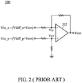
- FIG. 2 depicts another differential to single-ended buffer amplifier 200, which is implemented by a differential to single-ended operational amplifier 202, and is a differential amplifier that amplifies a voltage difference, (Vin_p - Vin n), between the positive and negative input terminals of the differential to single-ended buffer amplifier 200.
- the common-mode noise superimposed on both the positive and negative input terminals is therefore suppressed.
- no additional common-mode feedback circuit, such as CMFB of FIG. 1 is required.
- there is a significant signal swing at the non-inverting input terminal (Vx+) of the differential to single-ended operational amplifier 202 which degrades the linearity of the differential to single-ended buffer amplifier 200.
- a high-linearity differential to single-ended buffer amplifier is proposed in the present invention.
- a differential to single-ended buffer amplifier in accordance with an exemplary embodiment of the present invention has a positive input terminal, a negative input terminal, a differential to single-ended operational amplifier, and a swing suppression resistor.
- the differential to single-ended operational amplifier has a non-inverting input terminal and an inverting input terminal respectively coupled to the positive input terminal and the negative input terminal, and it has a single-ended output terminal that outputs the output signal of the differential to single-ended buffer amplifier.
- the swing suppression resistor is coupled between the negative input terminal of the differential to single-ended buffer amplifier and the non-inverting input terminal of the differential to single-ended operational amplifier. Accordingly, a signal swing at the non-inverting input terminal of the differential to single-ended operational amplifier is suppressed, wherein the signal swing is caused by a vibration of a differential part of an input signal of the differential to single-ended buffer amplifier.
- the differential to single-ended buffer amplifier further comprises a first resistor coupled between the positive input terminal of the differential to single-ended buffer amplifier and the non-inverting input terminal of the differential to single-ended operational amplifier.
- the resistance of the swing suppression resistor depends on the resistance of the first resistor.
- the first resistor and the swing suppression resistor have the same resistance, and so that the signal swing at the non-inverting input terminal of the differential to single-ended operational amplifier due to vibration of a differential part of an input signal of the differential to single-ended buffer amplifier can be completely eliminated.
- the differential to single-ended buffer amplifier further comprises a second resistor coupling the non-inverting input terminal of the differential to single-ended operational amplifier to ground. Resistance of the second resistor is n times the resistance of the first resistor.
- the gain of the differential to single-ended buffer amplifier is G. The value n depends on the gain G for common-mode noise suppression.
- the value n is half of G.
- the gain is between the output signal and the input signal of the differential to single-ended buffer amplifier.
- the output signal is the voltage at the single-ended output terminal of the differential to single-ended operational amplifier.
- the input signal is the voltage difference between the positive input terminal and the negative input terminal of the differential to single-ended buffer amplifier.
- the differential to single-ended buffer amplifier further comprises a third resistor and a fourth resistor.
- the third resistor is coupled between the negative input terminal of the differential to single-ended buffer amplifier and the inverting input terminal of the differential to single-ended operational amplifier.
- the fourth resistor is coupled between the inverting input terminal of the differential to single-ended operational amplifier and the single-ended output terminal of the differential to single-ended operational amplifier.
- the first resistor and the third resistor have the same resistance.
- the resistance of the fourth resistor is twice the resistance of the third resistor.
- FIG. 3 depicts a differential to single-ended buffer amplifier 300 in accordance with an exemplary embodiment of the present invention, which includes a positive input terminal Vin_p, a negative input terminal Vin n, a differential to single-ended operational amplifier (DISO op amp) 302, and a swing suppression resistor Rss.
- DISO op amp differential to single-ended operational amplifier
- the DISO op amp 302 has a non-inverting input terminal "+” and an inverting input terminal "-" coupled to the positive input terminal Vin_p (receiving a positive differential input Vdiff_p and a common-mode voltage Vcm) and negative input terminal Vin_n (receiving a negative differential input Vdiff_n and the common-mode voltage Vcm) of the differential to single-ended buffer amplifier 300, respectively, and has a single-ended output terminal outputting an output signal Vout of the differential to single-ended buffer amplifier 300.
- the swing suppression resistor Rss is coupled between the negative input terminal Vin n of the differential to single-ended buffer amplifier 300 and the non-inverting input terminal "+" of the DISO op amp 302.
- the differential to single-ended buffer amplifier 300 further comprises a first resistor R1 coupled between the positive input terminal Vin_p of the differential to single-ended buffer amplifier 300 and the non-inverting input terminal "+” of the DISO op amp 302.
- the resistance of the swing suppression resistor Rss depends on the resistance of the first resistor R1.
- the first signal swing portion at the non-inverting input terminal "+” due to the positive differential input Vdiff_p transferred through R1 may be compensated for by the second signal swing portion due to negative differential input Vdiff n transferred through Rss.
- FIG. 3 shows that the differential to single-ended buffer amplifier 300 further comprises a second resistor R2 coupling the non-inverting input terminal "+" of the DISO op amp 302 to ground.
- the gain of the differential to single-ended buffer amplifier 300 is G. The value n depends on the gain G for common-mode noise suppression.
- the output signal Vout is the voltage at the single-ended output terminal of the DISO op amp 302.
- the input signal Vin is the voltage difference between the positive input terminal Vin_p and the negative input terminal Vin n of the differential to single-ended buffer amplifier 300.
- FIG. 3 shows that the differential to single-ended buffer amplifier 300 further comprises a third resistor R3 and a fourth resistor R4.
- the third resistor R3 is coupled between the negative input terminal Vin_n of the differential to single-ended buffer amplifier 300 and the inverting input terminal "-" of the DISO op amp 302.
- the fourth resistor R4 is coupled between the inverting input terminal "-" of the DISO op amp 302 and the single-ended output terminal of the DISO op amp 302.
- the differential to single-ended buffer amplifier 300 successfully suppresses the common-mode noise as well as the non-ideal signal swing at the non-inverting input terminal of the DISO op amp 302.
- a high linearity buffer amplifier is provided.
- the differential to single-ended buffer amplifier 300 is in a differential amplification architecture that suppresses the common-mode noise Vcm noise by amplifying the input voltage difference, (Vin_p - Vin_n).
- Vin_p - Vin_n the input voltage difference
- the swing suppression resistor Rss may be applied to all kinds of differential amplification architecture.
- the forgoing resistors can be any resistance elements mentioned.
- the forgoing differential to single-ended operational amplifier is different from a fully-differential operational amplifier.
Landscapes
- Engineering & Computer Science (AREA)
- Power Engineering (AREA)
- Physics & Mathematics (AREA)
- Nonlinear Science (AREA)
- Amplifiers (AREA)
Abstract
Description
- The present invention relates to buffer amplifiers in a differential amplification architecture.
- A buffer amplifier (sometimes simply called a buffer) is one that provides electrical impedance transformation from one circuit to another, with the aim of preventing the signal source from being affected by the loading current.
- In some applications, the loading apparatus should be driven by a single-ended signal. A differential to single-ended buffer amplifier is required.
-
FIG. 1 depicts a differential to single-ended buffer amplifier 100 implemented by a fully differential (differential-in differential-out)operational amplifier 102. Only the positive output of the fully differentialoperational amplifier 102 is coupled to the loading apparatus as the output Vout of the differential to single-ended buffer amplifier 100. In such architecture, an additional common-mode feedback circuit CMFB is required to suppress common-mode noise. The common-mode noise may be generated in the wires and cables, due to electromagnetic induction, etc. Current flowing into the ground of a circuit from another circuit may result in a ground potential rise, which is another source of common-mode noise. -
FIG. 2 depicts another differential to single-ended buffer amplifier 200, which is implemented by a differential to single-endedoperational amplifier 202, and is a differential amplifier that amplifies a voltage difference, (Vin_p - Vin n), between the positive and negative input terminals of the differential to single-ended buffer amplifier 200. The common-mode noise superimposed on both the positive and negative input terminals is therefore suppressed. In such architecture, no additional common-mode feedback circuit, such as CMFB ofFIG. 1 , is required. However, there is a significant signal swing at the non-inverting input terminal (Vx+) of the differential to single-endedoperational amplifier 202, which degrades the linearity of the differential to single-ended buffer amplifier 200. - A high-linearity differential to single-ended buffer amplifier is proposed in the present invention.
- A differential to single-ended buffer amplifier in accordance with an exemplary embodiment of the present invention has a positive input terminal, a negative input terminal, a differential to single-ended operational amplifier, and a swing suppression resistor. The differential to single-ended operational amplifier has a non-inverting input terminal and an inverting input terminal respectively coupled to the positive input terminal and the negative input terminal, and it has a single-ended output terminal that outputs the output signal of the differential to single-ended buffer amplifier. The swing suppression resistor is coupled between the negative input terminal of the differential to single-ended buffer amplifier and the non-inverting input terminal of the differential to single-ended operational amplifier. Accordingly, a signal swing at the non-inverting input terminal of the differential to single-ended operational amplifier is suppressed, wherein the signal swing is caused by a vibration of a differential part of an input signal of the differential to single-ended buffer amplifier.
- In an exemplary embodiment, the differential to single-ended buffer amplifier further comprises a first resistor coupled between the positive input terminal of the differential to single-ended buffer amplifier and the non-inverting input terminal of the differential to single-ended operational amplifier. The resistance of the swing suppression resistor depends on the resistance of the first resistor.
- In an exemplary embodiment, the first resistor and the swing suppression resistor have the same resistance, and so that the signal swing at the non-inverting input terminal of the differential to single-ended operational amplifier due to vibration of a differential part of an input signal of the differential to single-ended buffer amplifier can be completely eliminated.
- In an exemplary embodiment, the differential to single-ended buffer amplifier further comprises a second resistor coupling the non-inverting input terminal of the differential to single-ended operational amplifier to ground. Resistance of the second resistor is n times the resistance of the first resistor. The gain of the differential to single-ended buffer amplifier is G. The value n depends on the gain G for common-mode noise suppression.
- In an exemplary embodiment, the value n is half of G.
- In an exemplary embodiment, the gain is between the output signal and the input signal of the differential to single-ended buffer amplifier. The output signal is the voltage at the single-ended output terminal of the differential to single-ended operational amplifier. The input signal is the voltage difference between the positive input terminal and the negative input terminal of the differential to single-ended buffer amplifier.
- In an exemplary embodiment, the differential to single-ended buffer amplifier further comprises a third resistor and a fourth resistor. The third resistor is coupled between the negative input terminal of the differential to single-ended buffer amplifier and the inverting input terminal of the differential to single-ended operational amplifier. The fourth resistor is coupled between the inverting input terminal of the differential to single-ended operational amplifier and the single-ended output terminal of the differential to single-ended operational amplifier.
- In an exemplary embodiment, the first resistor and the third resistor have the same resistance.
- In an exemplary embodiment, the resistance of the fourth resistor is twice the resistance of the third resistor.
- A detailed description is given in the following embodiments with reference to the accompanying drawings.
- The present invention can be more fully understood by reading the subsequent detailed description and examples with references made to the accompanying drawings, wherein:
-
FIG. 1 depicts a differential to single-ended buffer amplifier 100 implemented by a fully differential (differential-in differential-out)operational amplifier 102; -
FIG. 2 depicts another differential to single-ended buffer amplifier 200, which is implemented by a differential to single-endedoperational amplifier 202; and -
FIG. 3 depicts a differential to single-ended buffer amplifier 300 in accordance with an exemplary embodiment of the present invention, which includes a positive input terminal Vin_p, a negative input terminal Vin n, a differential to single-ended operational amplifier (DISO op amp) 302, and a swing suppression resistor Rss. - The following description is made for the purpose of illustrating the general principles of the invention and should not be taken in a limiting sense. The scope of the invention is best determined by reference to the appended claims.
-
FIG. 3 depicts a differential to single-ended buffer amplifier 300 in accordance with an exemplary embodiment of the present invention, which includes a positive input terminal Vin_p, a negative input terminal Vin n, a differential to single-ended operational amplifier (DISO op amp) 302, and a swing suppression resistor Rss. - The
DISO op amp 302 has a non-inverting input terminal "+" and an inverting input terminal "-" coupled to the positive input terminal Vin_p (receiving a positive differential input Vdiff_p and a common-mode voltage Vcm) and negative input terminal Vin_n (receiving a negative differential input Vdiff_n and the common-mode voltage Vcm) of the differential to single-ended buffer amplifier 300, respectively, and has a single-ended output terminal outputting an output signal Vout of the differential to single-ended buffer amplifier 300. - The swing suppression resistor Rss is coupled between the negative input terminal Vin n of the differential to single-
ended buffer amplifier 300 and the non-inverting input terminal "+" of theDISO op amp 302. - By the swing suppression resistor Rss, a signal swing at the non-inverting input terminal "+" of the
DISO op amp 302 due to vibration of a differential part (e.g., Vdiff_p and Vdiff n) of an input signal Vin of the differential to single-ended buffer amplifier 300 is suppressed. - As shown, the differential to single-
ended buffer amplifier 300 further comprises a first resistor R1 coupled between the positive input terminal Vin_p of the differential to single-ended buffer amplifier 300 and the non-inverting input terminal "+" of theDISO op amp 302. The resistance of the swing suppression resistor Rss depends on the resistance of the first resistor R1. In this architecture, the first signal swing portion at the non-inverting input terminal "+" due to the positive differential input Vdiff_p transferred through R1 may be compensated for by the second signal swing portion due to negative differential input Vdiff n transferred through Rss. - In an exemplary embodiment, the first resistor R1 and the swing suppression resistor Rss have the same resistance, e.g., Rss = R1. Thus, the signal swing at the non-inverting input terminal of the differential to single-ended operational amplifier due to vibration of a differential part of an input signal of the differential to single-ended buffer amplifier can be completely eliminated.
-
FIG. 3 shows that the differential to single-ended buffer amplifier 300 further comprises a second resistor R2 coupling the non-inverting input terminal "+" of theDISO op amp 302 to ground. The resistance of the second resistor R2 is n times the resistance of the first resistor R1, e.g., R2 = n∗R1. The gain of the differential to single-ended buffer amplifier 300 is G. The value n depends on the gain G for common-mode noise suppression. - In an exemplary embodiment, the value n is half of G, e.g., n = G/2.
- As shown in
FIG. 3 , the gain G is between the output signal Vout and the input signal Vin of the differential to single-ended buffer amplifier 300, e.g., G=Vout/Vin. The output signal Vout is the voltage at the single-ended output terminal of theDISO op amp 302. The input signal Vin is the voltage difference between the positive input terminal Vin_p and the negative input terminal Vin n of the differential to single-ended buffer amplifier 300. -
FIG. 3 shows that the differential to single-ended buffer amplifier 300 further comprises a third resistor R3 and a fourth resistor R4. The third resistor R3 is coupled between the negative input terminal Vin_n of the differential to single-ended buffer amplifier 300 and the inverting input terminal "-" of theDISO op amp 302. The fourth resistor R4 is coupled between the inverting input terminal "-" of theDISO op amp 302 and the single-ended output terminal of theDISO op amp 302. - In an exemplary embodiment, the first resistor R1 and the third resistor R3 have the same resistance, e.g., R1 = R3.
- In an exemplary embodiment, the resistance of the fourth resistor R4 may be twice the resistance of the third resistor R3, e.g., R4 = 2∗R3.
- In an exemplary embodiment wherein R1=R3=Rss and


buffer amplifier 300. - The differential to single-ended
buffer amplifier 300 successfully suppresses the common-mode noise as well as the non-ideal signal swing at the non-inverting input terminal of theDISO op amp 302. A high linearity buffer amplifier is provided. - The differential to single-ended
buffer amplifier 300 is in a differential amplification architecture that suppresses the common-mode noise Vcm noise by amplifying the input voltage difference, (Vin_p - Vin_n). There are many variants of the differential amplification architecture. The swing suppression resistor Rss may be applied to all kinds of differential amplification architecture. - Any differential to single-ended buffer amplifier with the swing suppression resistor Rss should be considered within the scope of the present invention.
- The forgoing resistors can be any resistance elements mentioned.
- The forgoing differential to single-ended operational amplifier is different from a fully-differential operational amplifier.
- While the invention has been described by way of example and in terms of the preferred embodiments, it should be understood that the invention is not limited to the disclosed embodiments. On the contrary, it is intended to cover various modifications and similar arrangements (as would be apparent to those skilled in the art). Therefore, the scope of the appended claims should be accorded the broadest interpretation so as to encompass all such modifications and similar arrangements.
Claims (12)
- A differential to single-ended buffer amplifier (300), comprising:a positive input terminal (Vin_p) and a negative input terminal (Vin n);a differential to single-ended operational amplifier (302), having a non-inverting input terminal and an inverting input terminal coupled to the positive input terminal and negative input terminal of the differential to single-ended buffer amplifier, respectively, and having a single-ended output terminal outputting an output signal of the differential to single-ended buffer amplifier; anda swing suppression resistor (Rss), coupled between the negative input terminal of the differential to single-ended buffer amplifier and the non-inverting input terminal of the differential to single-ended operational amplifier, and thereby a signal swing at the non-inverting input terminal of the differential to single-ended operational amplifier is suppressed, wherein the signal swing is caused by a vibration of a differential part of an input signal of the differential to single-ended buffer amplifier.
- The differential to single-ended buffer amplifier as claimed in claim 1, further comprising:a first resistor (R1), coupled between the positive input terminal of the differential to single-ended buffer amplifier and the non-inverting input terminal of the differential to single-ended operational amplifier,wherein resistance of the swing suppression resistor depends on resistance of the first resistor.
- The differential to single-ended buffer amplifier as claimed in claim 2, wherein the first resistor (R1) and the swing suppression resistor (Rss) have the same resistance.
- The differential to single-ended buffer amplifier as claimed in claim 3, further comprising:a second resistor (R2), coupling the non-inverting input terminal of the differential to single-ended operational amplifier to ground; andresistance of the second resistor is n times the resistance of the first resistor (R1);a gain of the differential to single-ended buffer amplifier is G; andn depends on G for common-mode noise suppression.
- The differential to single-ended buffer amplifier as claimed in claim 4, wherein:
n is half of G. - The differential to single-ended buffer amplifier as claimed in claim 5, wherein:the gain is between the output signal and the input signal of the differential to single-ended buffer amplifier;the output signal is a voltage at the single-ended output terminal of the differential to single-ended operational amplifier; andthe input signal is a voltage difference between the positive input terminal and the negative input terminal of the differential to single-ended buffer amplifier.
- The differential to single-ended buffer amplifier as claimed in claim 6, further comprising:a third resistor (R3), coupled between the negative input terminal of the differential to single-ended buffer amplifier and the inverting input terminal of the differential to single-ended operational amplifier; anda fourth resistor (R4), coupled between the inverting input terminal of the differential to single-ended operational amplifier and the single-ended output terminal of the differential to single-ended operational amplifier.
- The differential to single-ended buffer amplifier as claimed in claim 7, wherein:
the first resistor (R1) and the third resistor (R3) have the same resistance. - The differential to single-ended buffer amplifier as claimed in claim 8, wherein:
resistance of the fourth resistor (R4) is twice that of the third resistor (R3). - The differential to single-ended buffer amplifier as claimed in claim 2, further comprising:a second resistor (R2), coupling the non-inverting input terminal of the differential to single-ended operational amplifier to ground; andresistance of the second resistor is n times the resistance of the first resistor;gain of the differential to single-ended buffer amplifier is G; andn depends on G for common-mode noise suppression.
- The differential to single-ended buffer amplifier as claimed in claim 10, wherein:the gain is between the output signal and the input signal of the differential to single-ended buffer amplifier;the output signal is a voltage at the single-ended output terminal of the differential to single-ended operational amplifier; andthe input signal is a voltage difference between the positive input terminal and the negative input terminal of the differential to single-ended buffer amplifier.
- The differential to single-ended buffer amplifier as claimed in claim 11, further comprising:a third resistor (R3), coupled between the negative input terminal of the differential to single-ended buffer amplifier and the inverting input terminal of the differential to single-ended operational amplifier; anda fourth resistor (R4), coupled between the inverting input terminal of the differential to single-ended operational amplifier and the single-ended output terminal of the differential to single-ended operational amplifier.
Applications Claiming Priority (2)
| Application Number | Priority Date | Filing Date | Title |
|---|---|---|---|
| US202063010713P | 2020-04-16 | 2020-04-16 | |
| US17/184,805 US11502649B2 (en) | 2020-04-16 | 2021-02-25 | High-linearity differential to single ended buffer amplifier |
Publications (1)
| Publication Number | Publication Date |
|---|---|
| EP3896849A1 true EP3896849A1 (en) | 2021-10-20 |
Family
ID=75302328
Family Applications (1)
| Application Number | Title | Priority Date | Filing Date |
|---|---|---|---|
| EP21165919.8A Withdrawn EP3896849A1 (en) | 2020-04-16 | 2021-03-30 | High-linearity differential to single ended buffer amplifier |
Country Status (4)
| Country | Link |
|---|---|
| US (1) | US11502649B2 (en) |
| EP (1) | EP3896849A1 (en) |
| CN (1) | CN113541618A (en) |
| TW (1) | TWI786601B (en) |
Citations (2)
| Publication number | Priority date | Publication date | Assignee | Title |
|---|---|---|---|---|
| US3761831A (en) * | 1972-02-28 | 1973-09-25 | Bunker Ramo | Common mode rejection means for differential circuits |
| US5760648A (en) * | 1996-08-12 | 1998-06-02 | Motorola, Inc. | Electronic circuit for converting a differential signal into a single-ended signal with common mode voltage rejection by resistor network |
Family Cites Families (8)
| Publication number | Priority date | Publication date | Assignee | Title |
|---|---|---|---|---|
| NL8600292A (en) | 1986-02-07 | 1987-09-01 | Philips Nv | BRIDGE AMPLIFIER. |
| US5432476A (en) | 1993-04-09 | 1995-07-11 | National Semiconductor Corporation | Differential to single-ended converter |
| JP2004179900A (en) * | 2002-11-26 | 2004-06-24 | Tm T & D Kk | Common mode noise elimination circuit |
| US7233203B2 (en) * | 2005-08-05 | 2007-06-19 | Realtek Semiconductor Corp. | Differential amplifier |
| US8138830B2 (en) * | 2009-04-03 | 2012-03-20 | Qualcomm, Incorporated | Variable gain instrumentation amplifier |
| JP6512826B2 (en) * | 2015-01-05 | 2019-05-15 | 横河電機株式会社 | Differential amplifier |
| CN106470016B (en) * | 2015-08-20 | 2019-10-01 | 立锜科技股份有限公司 | Differential amplifier circuit |
| CN110932714B (en) * | 2019-12-18 | 2023-05-16 | 吉林大学 | Transmission interface circuit based on SUBLVDS |
-
2021
- 2021-02-25 US US17/184,805 patent/US11502649B2/en active Active
- 2021-03-30 EP EP21165919.8A patent/EP3896849A1/en not_active Withdrawn
- 2021-04-15 CN CN202110407109.7A patent/CN113541618A/en active Pending
- 2021-04-16 TW TW110113754A patent/TWI786601B/en active
Patent Citations (2)
| Publication number | Priority date | Publication date | Assignee | Title |
|---|---|---|---|---|
| US3761831A (en) * | 1972-02-28 | 1973-09-25 | Bunker Ramo | Common mode rejection means for differential circuits |
| US5760648A (en) * | 1996-08-12 | 1998-06-02 | Motorola, Inc. | Electronic circuit for converting a differential signal into a single-ended signal with common mode voltage rejection by resistor network |
Non-Patent Citations (1)
| Title |
|---|
| LOSMANDY ET AL: "Operational Amplifier Applications for Audio Systems", JOURNAL OF THE AUDIO ENGINEERING SOCIETY, AUDIO ENGINEERING SOCIETY, NEW YORK, NY, US, vol. 17, no. 1, 29 April 1968 (1968-04-29), pages 14 - 21, XP009102774, ISSN: 1549-4950 * |
Also Published As
| Publication number | Publication date |
|---|---|
| CN113541618A (en) | 2021-10-22 |
| US11502649B2 (en) | 2022-11-15 |
| TW202141926A (en) | 2021-11-01 |
| US20210328554A1 (en) | 2021-10-21 |
| TWI786601B (en) | 2022-12-11 |
Similar Documents
| Publication | Publication Date | Title |
|---|---|---|
| US7560969B2 (en) | Receiver of high speed digital interface | |
| CN102594273B (en) | DC offset tracking circuit and method thereof | |
| US6329876B1 (en) | Noise reduction scheme for operational amplifiers | |
| EP3826176A1 (en) | High-linearity input buffer | |
| US6160446A (en) | Balanced differential amplifier without common-mode feedback circuit | |
| CN111900940B (en) | Input stage clamping circuit, clamping method thereof and power amplifier | |
| KR100253727B1 (en) | An amplifier | |
| EP1501188A1 (en) | Differential amplifier | |
| EP1468489A1 (en) | Operational amplifier having improved input offset performance | |
| EP3139502B1 (en) | Single-ended to differential conversion circuit and signal processing module | |
| US9806703B2 (en) | Single-ended to differential conversion circuit and signal processing module | |
| US11502649B2 (en) | High-linearity differential to single ended buffer amplifier | |
| EP3713084B1 (en) | Low-noise differential to single-ended converter | |
| CN114337560A (en) | Differential amplifier | |
| US6040741A (en) | Preamplifier for amplifying signal voltages from a signal source with high source impedance | |
| EP4675920A1 (en) | Multi-stage amplifier using area-efficient and power-efficient common-mode termination technique | |
| JPH08148950A (en) | Balanced amplifier circuit | |
| KR102735229B1 (en) | Low Noise and Fully Differential Charge Amplifier | |
| US11469716B2 (en) | Limiting circuit and electronic device | |
| JP2000341095A (en) | Comparator circuit | |
| EP3826175A1 (en) | High-linearity amplifier | |
| JP4461480B2 (en) | amplifier | |
| CN120825364A (en) | Automotive LIN bus transmission integrated circuit | |
| JP2005079630A (en) | Floating power supply | |
| JP2023168757A (en) | Amplifier, amplifier circuit, and current detecting device |
Legal Events
| Date | Code | Title | Description |
|---|---|---|---|
| PUAI | Public reference made under article 153(3) epc to a published international application that has entered the european phase |
Free format text: ORIGINAL CODE: 0009012 |
|
| STAA | Information on the status of an ep patent application or granted ep patent |
Free format text: STATUS: THE APPLICATION HAS BEEN PUBLISHED |
|
| AK | Designated contracting states |
Kind code of ref document: A1 Designated state(s): AL AT BE BG CH CY CZ DE DK EE ES FI FR GB GR HR HU IE IS IT LI LT LU LV MC MK MT NL NO PL PT RO RS SE SI SK SM TR |
|
| B565 | Issuance of search results under rule 164(2) epc |
Effective date: 20210817 |
|
| STAA | Information on the status of an ep patent application or granted ep patent |
Free format text: STATUS: REQUEST FOR EXAMINATION WAS MADE |
|
| 17P | Request for examination filed |
Effective date: 20220316 |
|
| RBV | Designated contracting states (corrected) |
Designated state(s): AL AT BE BG CH CY CZ DE DK EE ES FI FR GB GR HR HU IE IS IT LI LT LU LV MC MK MT NL NO PL PT RO RS SE SI SK SM TR |
|
| P01 | Opt-out of the competence of the unified patent court (upc) registered |
Effective date: 20230607 |
|
| STAA | Information on the status of an ep patent application or granted ep patent |
Free format text: STATUS: EXAMINATION IS IN PROGRESS |
|
| 17Q | First examination report despatched |
Effective date: 20231005 |
|
| RAP3 | Party data changed (applicant data changed or rights of an application transferred) |
Owner name: MEDIATEK INC. |
|
| STAA | Information on the status of an ep patent application or granted ep patent |
Free format text: STATUS: THE APPLICATION IS DEEMED TO BE WITHDRAWN |
|
| 18D | Application deemed to be withdrawn |
Effective date: 20250910 |