EP3894794B1 - Apparatus for exciting a resolver and resolver arrangement - Google Patents
Apparatus for exciting a resolver and resolver arrangement Download PDFInfo
- Publication number
- EP3894794B1 EP3894794B1 EP19798630.0A EP19798630A EP3894794B1 EP 3894794 B1 EP3894794 B1 EP 3894794B1 EP 19798630 A EP19798630 A EP 19798630A EP 3894794 B1 EP3894794 B1 EP 3894794B1
- Authority
- EP
- European Patent Office
- Prior art keywords
- connection
- resolver
- node
- voltage
- output
- Prior art date
- Legal status (The legal status is an assumption and is not a legal conclusion. Google has not performed a legal analysis and makes no representation as to the accuracy of the status listed.)
- Active
Links
Images

Classifications
-
- H—ELECTRICITY
- H03—ELECTRONIC CIRCUITRY
- H03M—CODING; DECODING; CODE CONVERSION IN GENERAL
- H03M1/00—Analogue/digital conversion; Digital/analogue conversion
- H03M1/12—Analogue/digital converters
- H03M1/48—Servo-type converters
- H03M1/485—Servo-type converters for position encoding, e.g. using resolvers or synchros
-
- G—PHYSICS
- G01—MEASURING; TESTING
- G01D—MEASURING NOT SPECIALLY ADAPTED FOR A SPECIFIC VARIABLE; ARRANGEMENTS FOR MEASURING TWO OR MORE VARIABLES NOT COVERED IN A SINGLE OTHER SUBCLASS; TARIFF METERING APPARATUS; MEASURING OR TESTING NOT OTHERWISE PROVIDED FOR
- G01D5/00—Mechanical means for transferring the output of a sensing member; Means for converting the output of a sensing member to another variable where the form or nature of the sensing member does not constrain the means for converting; Transducers not specially adapted for a specific variable
- G01D5/12—Mechanical means for transferring the output of a sensing member; Means for converting the output of a sensing member to another variable where the form or nature of the sensing member does not constrain the means for converting; Transducers not specially adapted for a specific variable using electric or magnetic means
- G01D5/14—Mechanical means for transferring the output of a sensing member; Means for converting the output of a sensing member to another variable where the form or nature of the sensing member does not constrain the means for converting; Transducers not specially adapted for a specific variable using electric or magnetic means influencing the magnitude of a current or voltage
- G01D5/20—Mechanical means for transferring the output of a sensing member; Means for converting the output of a sensing member to another variable where the form or nature of the sensing member does not constrain the means for converting; Transducers not specially adapted for a specific variable using electric or magnetic means influencing the magnitude of a current or voltage by varying inductance, e.g. by a movable armature
- G01D5/204—Mechanical means for transferring the output of a sensing member; Means for converting the output of a sensing member to another variable where the form or nature of the sensing member does not constrain the means for converting; Transducers not specially adapted for a specific variable using electric or magnetic means influencing the magnitude of a current or voltage by varying inductance, e.g. by a movable armature by influencing the mutual induction between two or more coils
- G01D5/2086—Mechanical means for transferring the output of a sensing member; Means for converting the output of a sensing member to another variable where the form or nature of the sensing member does not constrain the means for converting; Transducers not specially adapted for a specific variable using electric or magnetic means influencing the magnitude of a current or voltage by varying inductance, e.g. by a movable armature by influencing the mutual induction between two or more coils by movement of two or more coils with respect to two or more other coils
-
- G—PHYSICS
- G01—MEASURING; TESTING
- G01D—MEASURING NOT SPECIALLY ADAPTED FOR A SPECIFIC VARIABLE; ARRANGEMENTS FOR MEASURING TWO OR MORE VARIABLES NOT COVERED IN A SINGLE OTHER SUBCLASS; TARIFF METERING APPARATUS; MEASURING OR TESTING NOT OTHERWISE PROVIDED FOR
- G01D3/00—Indicating or recording apparatus with provision for the special purposes referred to in the subgroups
- G01D3/08—Indicating or recording apparatus with provision for the special purposes referred to in the subgroups with provision for safeguarding the apparatus, e.g. against abnormal operation, against breakdown
-
- G—PHYSICS
- G01—MEASURING; TESTING
- G01D—MEASURING NOT SPECIALLY ADAPTED FOR A SPECIFIC VARIABLE; ARRANGEMENTS FOR MEASURING TWO OR MORE VARIABLES NOT COVERED IN A SINGLE OTHER SUBCLASS; TARIFF METERING APPARATUS; MEASURING OR TESTING NOT OTHERWISE PROVIDED FOR
- G01D5/00—Mechanical means for transferring the output of a sensing member; Means for converting the output of a sensing member to another variable where the form or nature of the sensing member does not constrain the means for converting; Transducers not specially adapted for a specific variable
- G01D5/12—Mechanical means for transferring the output of a sensing member; Means for converting the output of a sensing member to another variable where the form or nature of the sensing member does not constrain the means for converting; Transducers not specially adapted for a specific variable using electric or magnetic means
- G01D5/14—Mechanical means for transferring the output of a sensing member; Means for converting the output of a sensing member to another variable where the form or nature of the sensing member does not constrain the means for converting; Transducers not specially adapted for a specific variable using electric or magnetic means influencing the magnitude of a current or voltage
- G01D5/20—Mechanical means for transferring the output of a sensing member; Means for converting the output of a sensing member to another variable where the form or nature of the sensing member does not constrain the means for converting; Transducers not specially adapted for a specific variable using electric or magnetic means influencing the magnitude of a current or voltage by varying inductance, e.g. by a movable armature
- G01D5/204—Mechanical means for transferring the output of a sensing member; Means for converting the output of a sensing member to another variable where the form or nature of the sensing member does not constrain the means for converting; Transducers not specially adapted for a specific variable using electric or magnetic means influencing the magnitude of a current or voltage by varying inductance, e.g. by a movable armature by influencing the mutual induction between two or more coils
-
- G—PHYSICS
- G01—MEASURING; TESTING
- G01R—MEASURING ELECTRIC VARIABLES; MEASURING MAGNETIC VARIABLES
- G01R31/00—Arrangements for testing electric properties; Arrangements for locating electric faults; Arrangements for electrical testing characterised by what is being tested not provided for elsewhere
- G01R31/34—Testing dynamo-electric machines
- G01R31/346—Testing of armature or field windings
Definitions
- the present invention relates to a device for exciting a resolver, as well as a resolver arrangement with such a device.
- a device and a method for determining an angular position by means of a resolver is known, for example, from the publication DE 10 2009 005 494 A1
- an excitation winding of a resolver is excited with a reference signal and the resulting signals from two other windings of the resolver are sampled and evaluated using Fourier coefficients.
- An alternative device for exciting a resolver is known.
- An amplifier circuit with a switching bridge, a low-pass filter and an inductive load is known.
- the present invention discloses a device for exciting a resolver, as well as a resolver arrangement with the features of independent Patent claims. Further advantageous embodiments are the subject of the dependent patent claims.
- a resolver arrangement with a resolver and a device according to the invention for exciting the resolver comprises an excitation winding with a first excitation connection and a second excitation connection.
- the present invention is based on the knowledge that a conventional excitation of an excitation coil for a resolver generally requires a power amplification of an excitation signal.
- a current amplification with a push-pull output stage is preferably used in a conventional control.
- the transistors of such a push-pull output stage operate at least temporarily in a so-called linear mode and thus cause a high power loss.
- Such a push-pull output stage requires a relatively high input voltage compared to the output voltage.
- the input voltage must be at least twice as high as the desired signal amplitude at the output.
- the device comprises a second half-bridge.
- the second half-bridge comprises a third switching element arranged between the supply voltage and a second node, and a fourth switching element arranged between the second node and the reference potential.
- the second node is coupled to the second output terminal.
- the control device is designed to control the first switching element, the second switching element, the third switching element and the fourth switching element. Accordingly, a separate half-bridge is provided for both the first output terminal and the second output terminal.
- control device is implemented by means of a microcontroller or microprocessor. If necessary, suitable driver stages for the semiconductor switching elements are provided between the outputs of the microcontroller and the control terminals of the semiconductor switches.
- the first output terminal is designed to be coupled to a first excitation terminal of a resolver.
- the second output terminal is designed to be coupled to a second excitation terminal of a resolver.
- the device for exciting the resolver can be electrically coupled to the excitation coil of a resolver in order to excite the excitation coil of the resolver with a predetermined electrical voltage, in particular an electrical voltage with a predetermined amplitude and/or a predetermined frequency.
- the control device is designed to detect an electrical output voltage between the first output terminal and the second output terminal.
- the first, second, third and fourth switching elements of the first and second half-bridge can be controlled using the detected output voltage.
- the excitation voltage for the resolver can thus be precisely set between the first and second output terminal and thus at the excitation coil of a resolver.
- component tolerances and variations, for example due to thermal shifts, in the characteristic sizes of the components can be compensated in this way.
- the first low-pass filter comprises a first inductance and a first capacitor.
- the second low-pass filter comprises a second inductance and a second capacitor.
- the first inductance of the first low-pass filter is connected to the first node of the first half-bridge at a first connection. Furthermore, the first inductance is electrically coupled to the first output connection at a second connection.
- the first capacitor of the first low-pass filter is connected to the second connection of the first inductance at a first connection. Furthermore, the first capacitor is connected to the reference potential at a second connection.
- the second inductance of the second low-pass filter is connected to the second node of the second half-bridge at a first connection.
- the device for controlling a resolver comprises a first series capacitor and a second series capacitor.
- the first series capacitor is arranged in the current path between the first node and the first output connection.
- the second series capacitor is arranged in the current path between the second node and the second output connection.
- the first series capacitor and the second series capacitor are designed to form a series resonant circuit together with an excitation coil of a resolver that can be connected between the first output connection and the second output connection. If the capacitances of the two series capacitors are matched to the inductance of the excitation coil of the resolver and together form a series resonant circuit, this can achieve an increase in voltage. In this way, the excitation coil can be excited with a voltage that is higher than the electrical voltage provided between the first and second nodes of the half bridges. In particular, the voltage for exciting the excitation coil can be higher than the supply voltages of the device for exciting the resolver.
- the device for exciting a resolver comprises a first resistor and a second resistor.
- the first Resistor is arranged between the first output terminal and a third node.
- the second resistor is arranged between the second output terminal and the third node.
- the third node can be electrically coupled to a reference potential.
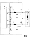
- Figure 1 shows a schematic representation of a basic circuit diagram as it is based on a device 1 for controlling a resolver 2 according to an embodiment.
- the device 1 for controlling the resolver 2 in this embodiment comprises a control device 10, a first half-bridge H1 and a second half-bridge H2.
- the first half-bridge H1 comprises a first switching element T1 and a second switching element T2.
- the first switching element T1 is connected to a supply voltage with one connection. Another connection of the first switching element T1 is connected to a first node K1.
- the control connection of the first switching element T1 is connected to the control device 10.
- the second switching element T2 is connected to the first node K1 with a first connection.
- a second connection of the control element T2 is connected to a reference potential.
- the switching elements T1 to T4 of the first and second half bridges H1 and H2 can be any switching elements.
- semiconductor switching elements for example MOSFET or similar, are possible.
- the present invention relates to the provision of an electrical voltage for exciting an excitation coil of a resolver.
- the electrical voltage for exciting the excitation coil of the resolver is generated by means of a pulse-width modulated control of at least one half-bridge.
- the switching elements of the half-bridges are fully switched through so that losses, such as those that occur in the linear operation of semiconductor switches, can be avoided. If necessary, the voltage provided by the half-bridge(s) can be additionally increased by means of suitable resonant circuits.
Landscapes
- Physics & Mathematics (AREA)
- General Physics & Mathematics (AREA)
- Engineering & Computer Science (AREA)
- Theoretical Computer Science (AREA)
- Transmission And Conversion Of Sensor Element Output (AREA)
Description
Die vorliegende Erfindung betrifft eine Vorrichtung zur Anregung eines Resolvers, sowie eine Resolveranordnung mit einer solchen Vorrichtung.The present invention relates to a device for exciting a resolver, as well as a resolver arrangement with such a device.
Resolver werden in zahlreichen Anwendungsbereichen zur Erfassung einer Winkellage von aktuierten oder nicht aktuierten Drehgelenken, Motoren oder ähnlichem verwendet. Zur Ansteuerung eines Resolvers wird in der Regel ein Erregersignal benötigt. Bei dem Erregersignal kann es sich beispielsweise um ein sinusförmiges Spannungssignal mit einer geeigneten Amplitude und Frequenz handeln. Um das Erregersignal mit einer ausreichenden Treiberleistung bereitzustellen wird in der Regel eine Verstärkerschaltung zur Spannungsverstärkung in Kombination mit einer Gegentaktendstufe zur Stromverstärkung eingesetzt.Resolvers are used in numerous applications to detect the angular position of actuated or non-actuated rotary joints, motors or similar. An excitation signal is usually required to control a resolver. The excitation signal can, for example, be a sinusoidal voltage signal with a suitable amplitude and frequency. In order to provide the excitation signal with sufficient driver power, an amplifier circuit for voltage amplification is usually used in combination with a push-pull output stage for current amplification.
Eine Vorrichtung und ein Verfahren zur Bestimmung einer Winkellage mittels eines Resolvers ist beispielsweise aus der Druckschrift
Die vorliegende Erfindung offenbart eine Vorrichtung zur Anregung eines Resolvers, sowie eine Resolveranordnung mit den Merkmalen der unabhängigen Patentansprüche. Weitere vorteilhafte Ausführungsformen sind Gegenstand der abhängigen Patentansprüche.The present invention discloses a device for exciting a resolver, as well as a resolver arrangement with the features of independent Patent claims. Further advantageous embodiments are the subject of the dependent patent claims.
Eine Vorrichtung zur Anregung eines Resolvers, wie in Anspruch 1 angegeben.An apparatus for exciting a resolver as set out in
Eine Resolveranordnung mit einem Resolver und einer erfindungsgemäßen Vorrichtung zur Anregung des Resolvers. Der Resolver umfasst eine Erregerwicklung mit einem ersten Erregeranschluss und einem zweiten Erregeranschluss.A resolver arrangement with a resolver and a device according to the invention for exciting the resolver. The resolver comprises an excitation winding with a first excitation connection and a second excitation connection.
Der vorliegenden Erfindung liegt die Erkenntnis zugrunde, dass eine konventionelle Anregung einer Erregerspule für einen Resolver in der Regel eine Leistungsverstärkung eines Erregersignals erfordert. Für diese Leistungsverstärkung wird bei einer konventionellen Ansteuerung vorzugsweise eine Stromverstärkung mit einer Gegentaktendstufe eingesetzt. Dabei arbeiten die Transistoren einer solchen Gegentaktendstufe zumindest zeitweise in einem sogenannten Linearbetrieb und verursachen somit eine hohe Verlustleistung.The present invention is based on the knowledge that a conventional excitation of an excitation coil for a resolver generally requires a power amplification of an excitation signal. For this power amplification, a current amplification with a push-pull output stage is preferably used in a conventional control. The transistors of such a push-pull output stage operate at least temporarily in a so-called linear mode and thus cause a high power loss.
Diese hohe Verlustleistung muss als thermische Energie abgeführt werden.This high power loss must be dissipated as thermal energy.
Darüber hinaus wird für eine solche Gegentaktendstufe im Vergleich zur Ausgangsspannung eine relativ hohe Eingangsspannung benötigt. In der Regel muss die Eingangsspannung mindestens doppelt so groß sein wie die gewünschte Signalamplitude am Ausgang.In addition, such a push-pull output stage requires a relatively high input voltage compared to the output voltage. As a rule, the input voltage must be at least twice as high as the desired signal amplitude at the output.
Der vorliegenden Erfindung liegt daher die Idee zugrunde, dieser Erkenntnis Rechnung zu tragen und eine verbesserte Ansteuerung der Erregerspule eines Resolvers vorzusehen. Insbesondere sollen die elektrischen Verluste während des Bereitstellens der Erregerspannung für den Resolver möglichst gering gehalten werden. Darüber hinaus soll vorzugsweise eine zur Verfügung stehende Versorgungsspannung möglichst effizient genutzt werden können.The present invention is therefore based on the idea of taking this knowledge into account and providing an improved control of the excitation coil of a resolver. In particular, the electrical losses during the provision of the excitation voltage for the resolver should be kept as low as possible. In addition, an available supply voltage should preferably be able to be used as efficiently as possible.
Hierzu ist erfindungsgemäß vorgesehen, die elektrische Spannung für die Erregerspule eines Resolvers unter Verwendung mindestens einer Halbbrücke zu erzeugen. Die einzelnen Schaltelemente in der Halbbrücken werden hierbei voll durchgeschaltet. Somit befinden sich die Schaltelemente im Gegensatz zu einer Gegentaktendstufe nicht in einem verlustreichen Linearbetrieb. Vielmehr wird eine Soll-Ausgangsspannung einer Halbbrücke mittels Pulsbreitenmodulation (Englisch: pulse width modulation, PWM) erzeugt.For this purpose, the invention provides for the electrical voltage for the excitation coil of a resolver to be generated using at least one half-bridge. The individual switching elements in the half-bridge are fully switched through. In contrast to a push-pull output stage, the switching elements are therefore not in lossy linear operation. Instead, a target output voltage of a half-bridge is generated using pulse width modulation (PWM).
Gemäß einer Ausführungsform umfasst die Vorrichtung eine zweite Halbbrücke. Die zweite Halbbrücke umfasst ein drittes Schaltelement, das zwischen der Versorgungsspannung und einem zweiten Knotenpunkt angeordnet ist, und ein viertes Schaltelement, das zwischen dem zweiten Knotenpunkt und dem Bezugspotential angeordnet ist. Der zweite Knotenpunkt ist mit dem zweiten Ausgangsanschluss gekoppelt. Die Steuereinrichtung ist dazu ausgelegt, das erste Schaltelement, das zweite Schaltelement, das dritte Schaltelement und das vierte Schaltelement anzusteuern. Entsprechend ist sowohl für den ersten Ausgangsanschluss als auch für den zweiten Ausgangsanschluss jeweils eine separate Halbbrücke vorgesehen.According to one embodiment, the device comprises a second half-bridge. The second half-bridge comprises a third switching element arranged between the supply voltage and a second node, and a fourth switching element arranged between the second node and the reference potential. The second node is coupled to the second output terminal. The control device is designed to control the first switching element, the second switching element, the third switching element and the fourth switching element. Accordingly, a separate half-bridge is provided for both the first output terminal and the second output terminal.
Die beiden Schaltelemente einer Halbbrücke werden dabei jeweils komplementär zueinander angesteuert. Somit ist entweder nur das Schaltelement zur positiven Versorgungsspannung oder das Schaltelement zur negativen Spannung bzw. dem Bezugspotential geschlossen. Gegebenenfalls kann zur Vermeidung eines Kurzschlusses auch eine Totzeit vorgesehen sein, in der beide Schaltelemente einer Halbbrücke geöffnet sind, bevor eines der beiden Schaltelemente geschlossen wird. Weiterhin können die Schaltelemente der zweiten Halbbrücke komplementär zu den Schaltelementen der ersten Halbbrücke angesteuert werden. Somit wird beispielsweise das Schaltelement der ersten Halbbrücke zwischen positiver Versorgungsspannung und Ausgang geschlossen, wenn in der zweiten Halbbrücke das Schaltelement zwischen negativer Spannung bzw. Bezugspotential geschlossen wird. Analog wird in der ersten Halbbrücke das Schaltelement zwischen Bezugspotential und Ausgangsspannung geschlossen, wenn in der zweiten Halbbrücke das Schaltelement zwischen positiver Versorgungsspannung und Ausgang geschlossen wird. Gegebenenfalls können je nach Anwendungsfall jedoch auch davon abweichende Schaltstrategien verwendet werden.The two switching elements of a half-bridge are controlled complementarily to each other. This means that either only the switching element for the positive supply voltage or the switching element for the negative voltage or the negative voltage is controlled. the reference potential is closed. If necessary, a dead time can also be provided to avoid a short circuit, in which both switching elements of a half-bridge are open before one of the two switching elements is closed. Furthermore, the switching elements of the second half-bridge can be controlled complementarily to the switching elements of the first half-bridge. For example, the switching element of the first half-bridge between the positive supply voltage and the output is closed when the switching element in the second half-bridge between the negative voltage or reference potential is closed. Similarly, the switching element in the first half-bridge between the reference potential and the output voltage is closed when the switching element in the second half-bridge between the positive supply voltage and the output is closed. However, depending on the application, different switching strategies can also be used.
Bei den Schaltelementen der ersten Halbbrücke und der zweiten Halbbrücke kann es sich beispielsweise um Halbleiterschaltelemente, wie zum Beispiel MOSFETs oder ähnliches handeln. Darüber hinaus sind selbstverständlich auch beliebige andere Schaltelemente, insbesondere beliebige andere Halbleiterschaltelemente möglich. Durch die Verwendung von Halbbrücken, bei denen jeweils die Schaltelemente voll durchgeschaltet werden, kann der volle Spannungsumfang zwischen positiver Versorgungsspannung und negativer Versorgungsspannung bzw. Bezugspotential genutzt werden. Auf diese Weise ist es möglich, die Erregerspannung für den Resolver besonders effizient und verlustarm zu generieren. Insbesondere können hohe elektrische Verluste, wie sie beispielsweise bei Gegentaktendstufen zur Anregung von Resolvern auftreten gemäß dem Stand der Technik, vermieden werden.The switching elements of the first half-bridge and the second half-bridge can be semiconductor switching elements, such as MOSFETs or similar. Of course, any other switching elements are also possible, in particular any other semiconductor switching elements. By using half-bridges, in which the switching elements are fully switched through, the full voltage range between the positive supply voltage and the negative supply voltage or reference potential can be used. In this way, it is possible to generate the excitation voltage for the resolver particularly efficiently and with low losses. In particular, high electrical losses, such as those that occur in push-pull output stages for exciting resolvers, can be avoided according to the state of the art.
Erfindungsgemäß ist Steuereinrichtung mittels eines Mikrocontrollers oder Mikroprozessors realisiert. Gegebenenfalls sind zwischen den Ausgängen des Mikrocontrollers und den Steueranschlüssen der Halbleiterschalter geeignete Treiberstufen für die Halbleiterschaltelemente vorgesehen.According to the invention, the control device is implemented by means of a microcontroller or microprocessor. If necessary, suitable driver stages for the semiconductor switching elements are provided between the outputs of the microcontroller and the control terminals of the semiconductor switches.
Gemäß einer Ausführungsform ist der erste Ausgangsanschluss dazu ausgelegt mit einem ersten Erregeranschluss eines Resolvers gekoppelt zu werden. Der zweite Ausgangsanschluss ist dazu ausgelegt, mit einem zweiten Erregeranschluss eines Resolvers gekoppelt zu werden. Auf diese Weise kann die Vorrichtung zur Anregung des Resolvers mit der Erregerspule eines Resolvers elektrisch gekoppelt werden, um die Erregerspule des Resolvers mit einer vorbestimmten elektrischen Spannung, insbesondere einer elektrischen Spannung mit einer vorgegebenen Amplitude und/oder einer vorgegebenen Frequenz anzuregen.According to one embodiment, the first output terminal is designed to be coupled to a first excitation terminal of a resolver. The second output terminal is designed to be coupled to a second excitation terminal of a resolver. In this way, the device for exciting the resolver can be electrically coupled to the excitation coil of a resolver in order to excite the excitation coil of the resolver with a predetermined electrical voltage, in particular an electrical voltage with a predetermined amplitude and/or a predetermined frequency.
Gemäß einer Ausführungsform ist die Steuereinrichtung dazu ausgelegt, an den Steuereingängen des ersten, zweiten, dritten und vierten Schaltelements jeweils ein pulsbreitenmoduliertes Steuersignal bereitzustellen. Durch eine pulsbreitenmodulierte Ansteuerung der Schaltelemente können die einzelnen Schaltelemente voll angesteuert, das heißt durchgeschaltet werden. Auf diese Weise werden die Schaltelemente nicht in einem verlustreichen Linearbetrieb betrieben. Die Frequenz der pulsbreitenmodulierten Steuerung ist dabei signifikant höher als die Grundfrequenz des Spannungssignals, das an der Erregerspule des Resolvers bereitgestellt werden soll. Beispielsweise kann die Frequenz der pulsbreitenmodulierten Ansteuerung das Zehnfache oder gegebenenfalls auch mehr der Grundfrequenz des Spannungssignals sein, das an der Erregerwicklung bereitgestellt werden soll.According to one embodiment, the control device is designed to provide a pulse-width modulated control signal at the control inputs of the first, second, third and fourth switching elements. By means of pulse-width modulated control of the switching elements, the individual switching elements can be fully controlled, i.e. switched through. In this way, the switching elements are not operated in a lossy linear mode. The frequency of the pulse-width modulated control is significantly higher than the fundamental frequency of the voltage signal that is to be provided at the excitation coil of the resolver. For example, the frequency of the pulse-width modulated control can be ten times or possibly more than the fundamental frequency of the voltage signal that is to be provided at the excitation winding.
Gemäß einer Ausführungsform ist die Steuereinrichtung dazu ausgelegt, eine elektrische Ausgangsspannung zwischen dem ersten Ausgangsanschluss und dem zweiten Ausgangsanschluss zu erfassen. Das erste, zweite, dritte und vierte Schaltelement der ersten und zweiten Halbbrücke kann in diesem Fall unter Verwendung der erfassten Ausgangsspannung angesteuert werden. Auf diese Weise kann ein geschlossener Regelkreis realisiert werden. Somit kann zwischen dem ersten und zweiten Ausgangsanschluss und somit an der Erregerspule eines Resolvers die Erregerspannung für den Resolver präzise eingestellt werden. Insbesondere können auf diese Weise Bauteiltoleranzen und Variationen, beispielsweise aufgrund von thermischen Verschiebungen, bei den charakteristischen Größen der Bauteile kompensiert werden.According to one embodiment, the control device is designed to detect an electrical output voltage between the first output terminal and the second output terminal. In this case, the first, second, third and fourth switching elements of the first and second half-bridge can be controlled using the detected output voltage. In this way, a closed control loop can be realized. The excitation voltage for the resolver can thus be precisely set between the first and second output terminal and thus at the excitation coil of a resolver. In particular, component tolerances and variations, for example due to thermal shifts, in the characteristic sizes of the components can be compensated in this way.
Gemäß einer Ausführungsform umfasst die Vorrichtung zur Anregung des Resolvers einen ersten Tiefpassfilter und einen zweiten Tiefpassfilter. Das erste Tiefpassfilter ist zwischen dem ersten Knotenpunkt der ersten Halbbrücke und dem ersten Ausgangsanschluss angeordnet. Das zweite Tiefpassfilter ist zwischen dem zweiten Knotenpunkt der zweiten Halbbrücke und dem zweiten Ausgangsanschluss angeordnet. Mittels der Tiefpassfilter können die höherfrequenten Anteile der pulsbreitenmodulierten Spannung herausgefiltert oder zumindest signifikant abgeschwächt werden. Darüber hinaus können die Tiefpassfilter einen Schwingkreis bilden, der bei Anregung im Bereich der Resonanzfrequenz eine Spannungserhöhung des Ausgangssignals und somit der Erregerspannung für den Resolver bewirken kann. In diesen Schwingkreis kann insbesondere auch die Induktivität des Resolvers mit einbezogen werden.According to one embodiment, the device for exciting the resolver comprises a first low-pass filter and a second low-pass filter. The first low-pass filter is arranged between the first node of the first half-bridge and the first output connection. The second low-pass filter is arranged between the second node of the second half-bridge and the second output connection. The low-pass filters can be used to filter out the higher frequency components of the pulse width modulated voltage or at least significantly attenuate them. In addition, the low-pass filters can form an oscillating circuit which, when excited in the range of the resonance frequency, can cause an increase in the voltage of the output signal and thus the excitation voltage for the resolver. In particular, the inductance of the resolver can also be included in this oscillating circuit.
Gemäß einer Ausführungsform umfasst das erste Tiefpassfilter eine erste Induktivität und einen ersten Kondensator. Das zweite Tiefpassfilter umfasst eine zweite Induktivität und einen zweiten Kondensator. Die erste Induktivität des ersten Tiefpassfilters ist an einem ersten Anschluss mit dem ersten Knotenpunkt der ersten Halbbrücke verbunden. Weiterhin ist die erste Induktivität an einem zweiten Anschluss mit dem ersten Ausgangsanschluss elektrisch gekoppelt. Der erste Kondensator des ersten Tiefpassfilters ist an einem ersten Anschluss mit dem zweiten Anschluss der ersten Induktivität verbunden. Weiterhin ist der erste Kondensator an einem zweiten Anschluss mit dem Bezugspotential verbunden. Die zweite Induktivität des zweiten Tiefpassfilters ist an einem ersten Anschluss mit dem zweiten Knotenpunkt der zweiten Halbbrücke verbunden. Weiterhin ist die zweite Induktivität an einem zweiten Anschluss mit dem zweiten Ausgangsanschluss elektrisch gekoppelt. Der zweite Kondensator des zweiten Tiefpassfilters ist an einem ersten Anschluss mit dem zweiten Anschluss der zweiten Induktivität verbunden. Weiterhin ist der zweite Kondensator an einem zweiten Anschluss mit dem Bezugspotential verbunden. Mittels einer solchen Konfiguration ist eine relativ einfache und kostengünstige Realisation von Tiefpassfiltern möglich. Insbesondere ist es auf diese Weise möglich, höherfrequente Anteile der pulsbreitenmodulierten Ansteuerung der Halbbrücken zu eliminieren und/oder eine Spannungserhöhung der bereitgestellten Signale zu realisieren.According to one embodiment, the first low-pass filter comprises a first inductance and a first capacitor. The second low-pass filter comprises a second inductance and a second capacitor. The first inductance of the first low-pass filter is connected to the first node of the first half-bridge at a first connection. Furthermore, the first inductance is electrically coupled to the first output connection at a second connection. The first capacitor of the first low-pass filter is connected to the second connection of the first inductance at a first connection. Furthermore, the first capacitor is connected to the reference potential at a second connection. The second inductance of the second low-pass filter is connected to the second node of the second half-bridge at a first connection. Furthermore, the second inductance is electrically coupled to the second output connection at a second connection. The second capacitor of the second low-pass filter is connected to the second connection of the second inductance at a first connection. Furthermore, the second capacitor is connected to the reference potential at a second connection. Such a configuration enables a relatively simple and cost-effective implementation of low-pass filters. In particular, it is possible in this way to eliminate higher frequency components of the pulse width modulated control of the half bridges and/or to realize a voltage increase of the signals provided.
Gemäß einer Ausführungsform umfasst die Vorrichtung zur Ansteuerung eines Resolvers einen ersten Serienkondensator und einen zweiten Serienkondensator. Der erste Serienkondensator ist in dem Strompfad zwischen dem ersten Knotenpunkt und dem ersten Ausgangsanschluss angeordnet. Der zweite Serienkondensator ist in dem Strompfad zwischen dem zweiten Knotenpunkt und dem zweiten Ausgangsanschluss angeordnet. Mittels einer solchen Anordnung von Serienkondensatoren können die Halbbrücken von dem Resolver galvanisch getrennt werden. Auf diese Weise ist ein Schutz der Anordnung, insbesondere der Halbbrücken möglich. Insbesondere ist es mittels der Serienkondensatoren möglich, die Bauelemente der Halbbrücken, wie z.B. die Halbleiterschalter der Halbbrücken, im Falles von Überlast oder bei einem Kurzschluss zu schützen und ggf. irreversiblen Beschädigungen vorzubeugen. Darüber hinaus können die Serienkondensatoren in Kombination mit der Induktivität der Erregerspule des Resolvers einen Schwingkreis bilden. Ferner können auch eventuell vorhandene Induktivitäten von Filterelementen, beisielsweise der oben erwähnten Tiefpassfilter, mit in den Schwingkreis einbezogen werden. Auch dieser Schwingkreis kann zur Spannungserhöhung der Erregerspannung genutzt werden.According to one embodiment, the device for controlling a resolver comprises a first series capacitor and a second series capacitor. The first series capacitor is arranged in the current path between the first node and the first output connection. The second series capacitor is arranged in the current path between the second node and the second output connection. By means of such an arrangement of series capacitors, the half-bridges can be galvanically isolated from the resolver. In this way, protection of the arrangement, in particular of the half-bridges, is possible. In particular, by means of the series capacitors it is possible to protect the components of the half-bridges, such as the semiconductor switches of the half-bridges, in the event of overload or a short circuit and to prevent any irreversible damage. In addition, the series capacitors can form an oscillating circuit in combination with the inductance of the excitation coil of the resolver. Furthermore, any inductances of filter elements that may be present, for example the low-pass filters mentioned above, can also be included in the oscillating circuit. This oscillating circuit can also be used to increase the excitation voltage.
Gemäß einer Ausführungsform sind der erste Serienkondensator und der zweite Serienkondensator dazu ausgelegt, gemeinsam mit einer zwischen dem ersten Ausgangsanschluss und dem zweiten Ausgangsanschluss anschließbaren Erregerspule eines Resolvers einen Serienschwingkreis zu bilden. Sind die Kapazitäten der beiden Serienkondensatoren auf die Induktivität der Erregerspule des Resolvers abgestimmt und bilden zusammen einen Serienschwingkreis, so kann hierdurch eine Spannungserhöhung erreicht werden. Auf diese Weise kann die Erregerspule mit einer Spannung angeregt werden, welche höher ist als die zwischen dem ersten und zweiten Knotenpunkte der Halbbrücken bereitgestellte elektrische Spannung. Insbesondere kann die Spannung zur Anregung der Erregerspule größer sein als die Versorgungsspannungen der Vorrichtung zur Anregung des Resolvers.According to one embodiment, the first series capacitor and the second series capacitor are designed to form a series resonant circuit together with an excitation coil of a resolver that can be connected between the first output connection and the second output connection. If the capacitances of the two series capacitors are matched to the inductance of the excitation coil of the resolver and together form a series resonant circuit, this can achieve an increase in voltage. In this way, the excitation coil can be excited with a voltage that is higher than the electrical voltage provided between the first and second nodes of the half bridges. In particular, the voltage for exciting the excitation coil can be higher than the supply voltages of the device for exciting the resolver.
Gemäß einer Ausführungsform umfasst die Vorrichtung zur Anregung eines Resolvers einen ersten Widerstand und einen zweiten Widerstand. Der erste Widerstand ist zwischen dem ersten Ausgangsanschluss und einem dritten Knotenpunkt angeordnet. Der zweite Widerstand ist zwischen dem zweiten Ausgangsanschluss und dem dritten Knotenpunkt angeordnet. Ferner kann der dritte Knotenpunkt mit einem Bezugspotential elektrisch gekoppelt sein. Durch eine solche Konfiguration zweier Widerstände, insbesondere zweier hochohmiger Widerstände, kann eine Symmetrisierung der elektrischen Spannung zwischen den beiden Ausgangsanschlüssen bezüglich des Bezugspotentials erreicht werden.According to one embodiment, the device for exciting a resolver comprises a first resistor and a second resistor. The first Resistor is arranged between the first output terminal and a third node. The second resistor is arranged between the second output terminal and the third node. Furthermore, the third node can be electrically coupled to a reference potential. By means of such a configuration of two resistors, in particular two high-resistance resistors, a symmetrization of the electrical voltage between the two output terminals with respect to the reference potential can be achieved.
Alternativ ist es auch möglich dass der erste Widerstand zwischen dem ersten Ausgangsanschuss und einem ersten Spannungspotential angeordnet ist, und der zweite Widerstand zwischen dem zweiten Ausgangsanschuss und einem zweiten Spannungspotential angeordnet ist. Insbesondere kann eines der beiden Spanungspotentiales, z.B. das zweite Spannungspotential das Bezugspotential sein.Alternatively, it is also possible that the first resistor is arranged between the first output connection and a first voltage potential, and the second resistor is arranged between the second output connection and a second voltage potential. In particular, one of the two voltage potentials, e.g. the second voltage potential, can be the reference potential.
Die vorliegende Erfindung wird nachfolgend anhand der in den schematischen Figuren der Zeichnungen angegebenen Ausführungsbeispiele näher erläutert. Dabei zeigen:
- Figur 1:
- eine schematische Darstellung einer Resolveranordnung mit einer Vorrichtung zur Anregung eines Resolvers gemäß einer Ausführungsform;
- Figur 2:
- eine schematische Darstellung eines Blockschaltbilds einer Resolveranordnung mit einer Vorrichtung zur Anregung eines Resolvers gemäß einer weiteren Ausführungsform; und
- Figur 3:
- eine schematische Darstellung eines Blockschaltbilds einer Resolveranordnung mit einer Vorrichtung zur Anregung eines Resolvers gemäß noch einer weiteren Ausführungsform.
- Figure 1:
- a schematic representation of a resolver arrangement with a device for exciting a resolver according to an embodiment;
- Figure 2:
- a schematic representation of a block diagram of a resolver arrangement with a device for exciting a resolver according to a further embodiment; and
- Figure 3:
- a schematic representation of a block diagram of a resolver arrangement with a device for exciting a resolver according to yet another embodiment.
Bei den Schaltelementen T1 bis T4 der ersten und zweiten Halbbrücke H1 und H2 kann es sich um beliebige Schaltelemente handeln. Insbesondere sind Halbleiterschaltelemente, beispielsweise MOSFET oder ähnliches möglich.The switching elements T1 to T4 of the first and second half bridges H1 and H2 can be any switching elements. In particular, semiconductor switching elements, for example MOSFET or similar, are possible.
Die Steuereinrichtung 10 generiert pulsbreitenmodulierte Ansteuersignale zum getakteten Öffnen und Schließen der Schaltelemente T1 bis T4.The
In einer besonders einfachen Ausführungsform kann der erste Knotenpunkt K1 direkt mit einem ersten Ausgangsanschluss A1 verbunden werden. Analog kann der zweite Knotenpunkt K2 direkt mit einem zweiten Ausgangsanschluss A2 verbunden werden. Zwischen dem ersten Ausgangsanschluss A1 und dem zweiten Ausgangsanschluss A2 kann auf diese Weise eine elektrische Spannung U_e bereitgestellt werden. Diese elektrische Spannung U_e kann dazu genutzt werden, eine Erregerspule E eines Resolvers 2 zu speisen.In a particularly simple embodiment, the first node K1 can be connected directly to a first output connection A1. Similarly, the second node K2 can be connected directly to a second output connection A2. In this way, an electrical voltage U_e can be provided between the first output connection A1 and the second output connection A2. This electrical voltage U_e can be used to feed an excitation coil E of a
Zwischen den beiden Halbbrücken H1, H2 und den Ausgangsanschlüssen A1, A2 kann weiterhin eine Filtereinrichtung vorgesehen sein. Die Filtereinrichtung umfasst ein erstes Tiefpassfilter, das zwischen dem ersten Knotenpunkt K1 und dem ersten Ausgangsanschluss A1 vorgesehen sein kann. Weiterhin umfasst die Filtereinrichtung 21 ein zweites Tiefpassfilter, das zwischen dem zweiten Knotenpunkt K2 und dem zweiten Ausgangsanschluss A2 vorgesehen sein kann. Das erste Tiefpassfilter kann eine erste Induktivität L1 und eine erste Kapazität C1 umfassen. Die erste Induktivität L1 kann zwischen dem ersten Knotenpunkt K1 und dem ersten Ausgangsanschluss A1 vorgesehen sein. Der erste Kondensator C1 kann zwischen dem Bezugspotential und dem Anschluss der ersten Induktivität L1 vorgesehen sein, die dem ersten Ausgangsanschluss A1 zugewandt ist. Analog kann zwischen dem zweiten Knotenpunkt K2 und dem zweiten Ausgangsanschluss A2 eine zweite Induktivität L2 vorgesehen sein, und ein zweiter Kondensator C2 kann zwischen einem Bezugspotential und dem Anschluss der zweiten Induktivität L2, welche dem zweiten Ausgangsanschluss A2 zugewandt ist, vorgesehen sein. Auf diese Weise können mittels der beiden Tiefpassfilter höherfrequente Anteile der an den Knotenpunkten K1 und K2 bereitgestellten elektrischen Spannungssignale herausgefiltert oder zumindest reduziert werden. Darüber hinaus können durch die oben beschriebenen Tiefpassfilteranordnungen jeweils Schwingkreise gebildet werden. Werden diese Schwingkreise im Bereich der Resonanzfrequenz angeregt, so ist hierdurch eine Spannungserhöhung der an den Knotenpunkten K1 und K2 bereitgestellten elektrischen Spannungen möglich. Auf diese Weise ist es prinzipiell möglich, an den Ausgangsanschlüssen A1 und A2 eine elektrische Spannung bereitzustellen, welche gegebenenfalls sogar höher ist als die Versorgungsspannung, welche die Halbbrücken H1 und H2 speist.A filter device can also be provided between the two half-bridges H1, H2 and the output connections A1, A2. The filter device comprises a first low-pass filter, which can be provided between the first node K1 and the first output connection A1. The
Zur Erzeugung der Erregerspannung U_e für eine Erregerspule E eines Resolvers 2 werden das erste, zweite, dritte und vierte Schaltelement T1 bis T4 von der Steuereinrichtung 10 in geeigneter Weise angesteuert. Insbesondere erfolgt hierbei eine pulsbreitenmodulierte Ansteuerung der vier Schaltelemente T1 bis T4. Bei dieser Ansteuerung sind die angesteuerten Schaltelemente jeweils vollständig durchgeschaltet, das heißt geschlossen. Im nicht angesteuerten Zustand sind die entsprechenden Schaltelemente vollständig geöffnet. Es erfolgt somit kein Linearbetrieb der Schaltelemente, in denen die Schaltelemente jeweils nur teilweise leitend sind.To generate the excitation voltage U_e for an excitation coil E of a
Die Steuereinrichtung 10 steuert die beiden Schaltelemente T1 bis T4 der Halbbrücken H1 und H2 jeweils komplementär an. Das heißt, es ist entweder das obere Schaltelement T1 bzw. T3 leitend, welches mit der Versorgungsspannung verbunden ist, oder ist alternativ das untere Schaltelement T2, T4 leitend, welches mit dem Bezugspotential verbunden ist. Gegebenenfalls kann bei einem Wechsel der Ansteuerung jeweils eine vorgegebene Totzeit vorgesehen sein, in der sowohl das obere (T1, T3) als auch das untere (T2, T4) Schaltelement gleichzeitig geöffnet sind. Auf diese Weise kann sichergestellt werden, dass ein Kurzschluss zwischen der Versorgungsspannung und dem Bezugspotential während des Schaltvorgangs vermieden wird. Die Trägerfrequenz der pulsbreitenmodulierten Ansteuerung der Schaltelemente T1 bis T4 ist dabei signifikant größer als eine Grundfrequenz des Erregersignals U_e, welches an der Erregerspule E des Resolvers 2 bereitgestellt werden soll. Beispielsweise kann die pulsbreitenmodulierte Ansteuerung mit einer Taktrate von dem Zehnfachen oder mehr der Grundfrequenz erfolgen.The
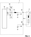
Wie in
Je nach Anwendungsfall können gegebenenfalls anstelle der Induktivitäten L1,L2 auch Widerstände oder andere geeignete elektriche Bauelemente eingesetzt werden.Depending on the application, resistors or other suitable electrical components can be used instead of the inductors L1, L2.
Darüber hinaus ist es beispielsweise mittels des Moduls 23 möglich, das Gleichspannungspotential der Ausgangsspannung U_e einzustellen. Hierzu kann ein erster Widerstand R1 zwischen dem ersten Ausgangsanschluss A1 und einem dritten Knotenpunkt K3 vorgesehen sein. Weiterhin kann ein zweiter Widerstand R2 zwischen dem zweiten Ausgangsanschluss A2 und dem dritten Knotenpunkt K3 vorgesehen sein. Gegebenenfalls kann der dritte Knotenpunkt K3 mit einem Bezugspotential oder einem vorgegebenen Spannungspotential verbunden sein.In addition, it is possible, for example, to adjust the direct voltage potential of the output voltage U_e using the
Alternativ ist es auch möglich, dass der erste Widerstand R1 und der zweite Widerstand R2 nicht an einem gemeinsamen dritten Knotenpunkt K3 miteinander verbunden sind. Beispielsweise kann der erste Widerstand R1 zwischen dem ersten Ausgangsanschluss A1 und einem ersten Spannungspotenzial angeordnet sein, und der zweite Widerstand R2 kann zwischen den zweiten Ausgangsanschluss A2 und einem zweiten Spannungpotenzial angeordnet sein. Hierbei kann eines der beiden Spannungspotenziale beispielsweise ein Bezugspotenzial sein.Alternatively, it is also possible that the first resistor R1 and the second resistor R2 are not connected to one another at a common third node K3. For example, the first resistor R1 can be arranged between the first output terminal A1 and a first voltage potential, and the second resistor R2 can be arranged between the second output terminal A2 and a second voltage potential. In this case, one of the two voltage potentials can be a reference potential, for example.
Bei dem ersten Widerstand R1 und den zweiten Widerstand R2 kann es sich insbesondere um relativ hochohmige Widerstände im Bereich von Kiloohm oder gegebenenfalls Megaohm handeln.The first resistor R1 and the second resistor R2 can in particular be relatively high-ohm resistors in the range of kiloohms or possibly megaohms.
Für einen geschlossenen Regelkreis kann die zwischen dem ersten Ausgangsanschluss A1 und dem zweiten Ausgangsanschluss A2 bereitgestellte Ausgangsspannung U_e direkt oder über eine beliebige geeignete Erfassungsschaltung an der Steuereinrichtung 10 bereitgestellt werden. Auf diese Weise kann die Steuereinrichtung 10 die pulsbreitenmodulierte Ansteuerung der Schaltelemente T1 bis T4 der ersten und zweiten Halbbrücke unter Verwendung der erfassten Ausgangsspannung U_e anpassen. Dies ermöglicht ein sehr präzises Einstellen der Ausgangsspannung U_e. Insbesondere können auf diese Weise auch Bauteiltoleranzen der Komponenten der Vorrichtung 1 sowie Variationen in den charakteristischen Größen der Erregerspule E des Resolvers 2 kompensiert werden. Ferner ist es auch möglich, Schwankungen in den charakteristischen Größen der Bauteile, beispielsweise aufgrund von Erwärmungen oder Abkühlungen, Alterungseffekten oder ähnlichem zu berücksichtigen und zu kompensieren.For a closed control loop, the output voltage U_e provided between the first output terminal A1 and the second output terminal A2 can be provided to the
Bei der Steuereinrichtung 10 kann es sich um eine beliebige Steuereinrichtung handeln, welche dazu geeignet ist, Steuersignale für eine pulsbreitenmodulierte Ansteuerung der Schaltelemente T1 bis T4 der ersten und zweiten Halbbrücke H1, H2 bereitzustellen. Gegebenenfalls können die von der Steuereinrichtung 10 bereitgestellten Steuersignale mittels geeigneter Treiberstufen (nicht dargestellt) verstärkt werden, um die entsprechende Leistung zur Ansteuerung der Schaltelemente T1 bis T4 bereitzustellen. Die Steuereinrichtung 10 kann beispielsweise mittels eines entsprechend konfigurierten bzw. programmierten Mikrocontrollers oder ähnlichem realisiert werden.The
In einer weiteren Ausführungsform kann beispielsweise eine der beiden Halbbrücken H1 oder H2 entfallen.
Bei einer Vorrichtung 1 mit nur eine Halbbrücke K1 kann beispielsweise der zweite Ausgangsanschluss A2 über einen Kondensator, hier als Kondensator C5 dargestellt, mit einem Spannungspotenzial, beispielsweise dem Bezugspotenzial verbunden sein. In diesem Fall kann die Kapazität des Kondensators C5 relativ groß bemessen sein.In a
Zusammenfassend betrifft die vorliegende Erfindung das Bereitstellen einer elektrischen Spannung zur Anregung einer Erregerspule eines Resolvers. Die elektrische Spannung zur Anregung der Erregerspule des Resolvers wird dabei mittels einer pulsbreitenmodulierten Ansteuerung mindestens einer Halbbrücken generiert. Dabei werden die Schaltelemente der Halbbrücken voll durchgeschaltet, so dass Verluste, wie sie beispielsweise im Linearbetrieb von Halbleiterschaltern auftreten, vermieden werden können. Gegebenenfalls kann mittels geeigneter Schwingkreise die von der oder den Halbbrücken bereitgestellte Spannung zusätzlich erhöht werden.In summary, the present invention relates to the provision of an electrical voltage for exciting an excitation coil of a resolver. The electrical voltage for exciting the excitation coil of the resolver is generated by means of a pulse-width modulated control of at least one half-bridge. The switching elements of the half-bridges are fully switched through so that losses, such as those that occur in the linear operation of semiconductor switches, can be avoided. If necessary, the voltage provided by the half-bridge(s) can be additionally increased by means of suitable resonant circuits.
Claims (12)
- Device (1) for exciting a resolver (2), having:a first output connection (A1), designed to be coupled to a first excitation connection of the resolver (2),a second output connection (A2), designed to be coupled to a second excitation connection of the resolver (2),a first half-bridge (H1), having a first switching element (T1), which is arranged between a supply voltage and a first node (K1), and a second switching element (T2), which is arranged between the first node (K1) and a reference-earth potential, the first node (K1) being coupled to the first output connection (A1); anda control apparatus (10), designed to control the first switching element (T1) and the second switching element (T2),characterized in thatthe control apparatus (10) is realized bya microcontroller or a microprocessor and is designed to provide a pulse-width-modulated control signal at each of the control inputs of the switching elements (T1 to T4), the individual switching elements (T1, T2) in the half-bridge being switched on to the full extent.
- Device (1) according to Claim 1, having a first low-pass filter, which is arranged between the first node (K1) and the first output connection (A1).
- Device (1) according to Claim 2, wherein the first low-pass filter comprises a first inductor (L1) and a first capacitor (C1), wherein the first inductor (L1) is connected by a first connection to the first node (K1) of the first half-bridge (H1) and is electrically coupled by a second connection to the first output connection (A1), and the first capacitor (C1) is connected by a first connection to the second connection of the first inductor (L1) and is connected by a second connection to the reference-earth potential.
- Device (1) according to one of Claims 1 to 3, having a second half-bridge (H2) having a third switching element (T3), which is arranged between the supply voltage and a second node (K2), and a fourth switching element (T4), which is arranged between the second node (K2) and the reference-earth potential, the second node (K2) being coupled to the second output connection (A2);
wherein the control apparatus (10) is designed to control the first switching element (T1), the second switching element (T2), the third switching element (T3) and the fourth switching element (T4). - Device (1) according to one of Claims 1 to 4, wherein the control apparatus (10) is designed to detect an electrical output voltage (U_e) between the first output connection (A1) and the second output connection (A2), and to control the switching elements (T1 to T4) using the detected output voltage (U_e).
- Device (1) according to one of Claims 1 to 5, having a second low-pass filter, which is arranged between the second node (K2) and the second output connection (A2).
- Device (1) according to Claim 6,
wherein the second low-pass filter comprises a second inductor (L2) and a second capacitor (C2), wherein the second inductor (L2) is connected by a first connection to the second node (K2) of the second half-bridge (H2) and is electrically coupled by a second connection to the second output connection (A2), and the second capacitor (C2) is connected by a first connection to the second connection of the second inductor (L2) and is connected by a second connection to the reference-earth potential. - Device (1) according to one of Claims 4 to 7, having a first series capacitor (C3), which is arranged between the first node (K1) and the first output connection (A1); and
having a second series capacitor (C4), which is arranged between the second node (K2) and the second output connection (A2). - Device (1) according to Claim 8, wherein the first series capacitor (C3) and the second series capacitor (C4) are designed to form a series resonant circuit with a field coil (E) of a resolver (2), which field coil is connectable between the first output connection (A1) and the second output connection (A2).
- Device (1) according to one of Claims 4 to 9, having a first resistor (R1), which is arranged between the first output connection (A1) and a first voltage potential, and
having a second resistor (R2), which is arranged between the second output connection (A2) and a fourth voltage potential. - Device according to Claim 10, wherein the third voltage potential and the fourth voltage potential are identical.
- Resolver arrangement, having:a resolver (2), comprising a field coil (E) having a first excitation connection and a second excitation connection; anda device (1) for exciting the resolver (2) according to one of Claims 1 to 11.
Applications Claiming Priority (2)
| Application Number | Priority Date | Filing Date | Title |
|---|---|---|---|
| DE102018221295.3A DE102018221295A1 (en) | 2018-12-10 | 2018-12-10 | Device for excitation of a resolver and resolver arrangement |
| PCT/EP2019/080377 WO2020120035A1 (en) | 2018-12-10 | 2019-11-06 | Device for exciting a resolver, and resolver arrangement |
Publications (2)
| Publication Number | Publication Date |
|---|---|
| EP3894794A1 EP3894794A1 (en) | 2021-10-20 |
| EP3894794B1 true EP3894794B1 (en) | 2025-01-08 |
Family
ID=68470527
Family Applications (1)
| Application Number | Title | Priority Date | Filing Date |
|---|---|---|---|
| EP19798630.0A Active EP3894794B1 (en) | 2018-12-10 | 2019-11-06 | Apparatus for exciting a resolver and resolver arrangement |
Country Status (5)
| Country | Link |
|---|---|
| US (1) | US11994413B2 (en) |
| EP (1) | EP3894794B1 (en) |
| CN (1) | CN113167600A (en) |
| DE (1) | DE102018221295A1 (en) |
| WO (1) | WO2020120035A1 (en) |
Families Citing this family (4)
| Publication number | Priority date | Publication date | Assignee | Title |
|---|---|---|---|---|
| CN116191973A (en) * | 2022-07-06 | 2023-05-30 | 方地应用技术(上海)有限公司 | A Resolver Angle Detection System with Square Wave Excitation |
| US20240337511A1 (en) * | 2023-04-05 | 2024-10-10 | Microchip Technology Incorporated | H-bridge push-pull excitation circuit for a transformer-based measuring device |
| WO2024210952A1 (en) * | 2023-04-05 | 2024-10-10 | Microchip Technology Incorporated | H-bridge push-pull excitation circuit for a resolver |
| US12535539B2 (en) * | 2023-09-29 | 2026-01-27 | Texas Instruments Incorporated | Fault detection front end architecture in resolver |
Family Cites Families (15)
| Publication number | Priority date | Publication date | Assignee | Title |
|---|---|---|---|---|
| US4894621A (en) * | 1988-06-13 | 1990-01-16 | Westinghouse Electric Corp. | Circuit for five level waveform synthesis |
| JP4682813B2 (en) * | 2005-11-11 | 2011-05-11 | パナソニック株式会社 | Power supply |
| DE102009005494A1 (en) | 2009-01-21 | 2010-07-22 | Kuka Roboter Gmbh | Method and device for determining an angular position by means of a resolver |
| JP5428688B2 (en) | 2009-09-14 | 2014-02-26 | 株式会社ジェイテクト | Motor control device and electric power steering device |
| DE112012005053B4 (en) | 2012-02-24 | 2019-05-16 | Aisin Aw Co., Ltd. | Resolver excitation device |
| CN103759773B (en) | 2014-02-18 | 2016-03-09 | 北京中锐智诚科技有限公司 | Field voltage method of adjustment, control circuit and electromagnetic flowmeter field circuit |
| US9778071B2 (en) | 2014-06-12 | 2017-10-03 | Lear Corporation | Excitation signal generator for resolver |
| JP6109370B1 (en) | 2016-03-22 | 2017-04-05 | 三菱電機株式会社 | Rotation angle detector |
| JP2017175586A (en) * | 2016-03-25 | 2017-09-28 | ヤマハ株式会社 | Self-excited class d amplifier of btl output |
| US10700589B2 (en) * | 2016-04-29 | 2020-06-30 | Massachusetts Institute Of Technology | Wide-operating-range resonant-transition soft-switched converter |
| CN107478279A (en) | 2016-06-08 | 2017-12-15 | 西尼尔(南京)过程控制有限公司 | Electromagnetic flowmeter and its excitation voltage regulation method |
| DE102016220358A1 (en) * | 2016-10-18 | 2018-04-19 | Robert Bosch Gmbh | DC-DC converter and method for driving a DC-DC converter |
| JP6806532B2 (en) | 2016-11-09 | 2021-01-06 | アズビル株式会社 | Excitation circuit of electromagnetic flowmeter, and electromagnetic flowmeter |
| CN107659224B (en) | 2017-08-18 | 2020-03-06 | 天津大学 | Device and method for rotary transformer shaft angle conversion based on square wave excitation signal |
| US11005356B2 (en) * | 2018-11-07 | 2021-05-11 | Rohm Co., Ltd. | Power supply control device and LLC resonant converter |
-
2018
- 2018-12-10 DE DE102018221295.3A patent/DE102018221295A1/en not_active Withdrawn
-
2019
- 2019-11-06 EP EP19798630.0A patent/EP3894794B1/en active Active
- 2019-11-06 CN CN201980081589.3A patent/CN113167600A/en active Pending
- 2019-11-06 WO PCT/EP2019/080377 patent/WO2020120035A1/en not_active Ceased
- 2019-11-06 US US17/312,915 patent/US11994413B2/en active Active
Also Published As
| Publication number | Publication date |
|---|---|
| US20220042827A1 (en) | 2022-02-10 |
| DE102018221295A1 (en) | 2020-06-10 |
| US11994413B2 (en) | 2024-05-28 |
| CN113167600A (en) | 2021-07-23 |
| EP3894794A1 (en) | 2021-10-20 |
| WO2020120035A1 (en) | 2020-06-18 |
Similar Documents
| Publication | Publication Date | Title |
|---|---|---|
| EP3894794B1 (en) | Apparatus for exciting a resolver and resolver arrangement | |
| EP2349041B1 (en) | Hf surgical generator | |
| DE102008034109B4 (en) | Circuit for simulating an electrical load | |
| DE10262286B4 (en) | A power supply device for generating high frequency power for a plasma generating device | |
| DE69838991T2 (en) | DRIVER FOR PIEZOELECTRIC ENGINES | |
| EP3840980B1 (en) | Charging apparatus with controllable intermediate circuit neutral point voltage and drive system with such charging apparatus | |
| WO2003077414A2 (en) | Power amplifier | |
| WO2002023204A1 (en) | Analytical circuit for a current sensor working on the compensation principle, in particular for the measurement of direct and alternating currents and method for operation of said current sensor | |
| WO2018210869A1 (en) | Inverter with intermediate circuit capacitor cascade and dc-side common-mode and differential-mode filters | |
| EP2036138B1 (en) | Device comprising piezo actuator | |
| DE4302056A1 (en) | Resonant inverter | |
| EP3667917A1 (en) | Control circuit for an oscillator circuit for operating parallel-fed oscillators | |
| EP2979311B1 (en) | Circuit assembly and method for controlling a piezoelectric transformer | |
| EP2945288A1 (en) | Circuit assembly and method for controlling a semiconductor switching element | |
| DE19810321A1 (en) | Current and charge regulation method for capacitive load e.g. piezoactuator operating in kHz range | |
| WO2020007812A1 (en) | Method for operating a circuit for producing an electromagnetic field, and circuit | |
| DE4023253A1 (en) | Harmonic-free DC power supply for bipolar load - uses concreted shorting of several sources of direct current sharing same deg. of pulse width modulation | |
| EP3410589B1 (en) | Inverter, device with such an inverter, system and method for controlling a controllable energy source | |
| DE4322608C2 (en) | Device for power modulation in plasma excitation, preferably when using gas lasers | |
| DE102022210189A1 (en) | DC-DC converter, electric vehicle and method for operating a DC-DC converter | |
| WO2007082601A1 (en) | Self-oscillating pwm controller for a single-phase ultrasonic motor | |
| DE3836950A1 (en) | CIRCUIT ARRANGEMENT FOR CONTROLLING A BRUSHLESS DC MOTOR | |
| DE102011089963A1 (en) | Pulse width modulation controller for use in micro-controller, outputs control signal, where slope of signal pulses of control signal is clocked with frequency that is larger than another frequency around specific factor | |
| EP2375551B1 (en) | Commutation method, commutation circuit and electric power converter | |
| DE102004019518A1 (en) | Method for optimal regulation or compensation of excess oscillations in current or voltage especially in power electronic circuits with active filters for machines uses fsrf reference values |
Legal Events
| Date | Code | Title | Description |
|---|---|---|---|
| STAA | Information on the status of an ep patent application or granted ep patent |
Free format text: STATUS: UNKNOWN |
|
| STAA | Information on the status of an ep patent application or granted ep patent |
Free format text: STATUS: THE INTERNATIONAL PUBLICATION HAS BEEN MADE |
|
| PUAI | Public reference made under article 153(3) epc to a published international application that has entered the european phase |
Free format text: ORIGINAL CODE: 0009012 |
|
| STAA | Information on the status of an ep patent application or granted ep patent |
Free format text: STATUS: REQUEST FOR EXAMINATION WAS MADE |
|
| 17P | Request for examination filed |
Effective date: 20210712 |
|
| AK | Designated contracting states |
Kind code of ref document: A1 Designated state(s): AL AT BE BG CH CY CZ DE DK EE ES FI FR GB GR HR HU IE IS IT LI LT LU LV MC MK MT NL NO PL PT RO RS SE SI SK SM TR |
|
| DAV | Request for validation of the european patent (deleted) | ||
| DAX | Request for extension of the european patent (deleted) | ||
| STAA | Information on the status of an ep patent application or granted ep patent |
Free format text: STATUS: EXAMINATION IS IN PROGRESS |
|
| 17Q | First examination report despatched |
Effective date: 20221214 |
|
| GRAP | Despatch of communication of intention to grant a patent |
Free format text: ORIGINAL CODE: EPIDOSNIGR1 |
|
| STAA | Information on the status of an ep patent application or granted ep patent |
Free format text: STATUS: GRANT OF PATENT IS INTENDED |
|
| RIC1 | Information provided on ipc code assigned before grant |
Ipc: H03M 1/48 20060101ALI20240927BHEP Ipc: G01D 5/20 20060101AFI20240927BHEP |
|
| INTG | Intention to grant announced |
Effective date: 20241014 |
|
| GRAS | Grant fee paid |
Free format text: ORIGINAL CODE: EPIDOSNIGR3 |
|
| GRAA | (expected) grant |
Free format text: ORIGINAL CODE: 0009210 |
|
| STAA | Information on the status of an ep patent application or granted ep patent |
Free format text: STATUS: THE PATENT HAS BEEN GRANTED |
|
| AK | Designated contracting states |
Kind code of ref document: B1 Designated state(s): AL AT BE BG CH CY CZ DE DK EE ES FI FR GB GR HR HU IE IS IT LI LT LU LV MC MK MT NL NO PL PT RO RS SE SI SK SM TR |
|
| REG | Reference to a national code |
Ref country code: GB Ref legal event code: FG4D Free format text: NOT ENGLISH |
|
| REG | Reference to a national code |
Ref country code: CH Ref legal event code: EP |
|
| REG | Reference to a national code |
Ref country code: DE Ref legal event code: R096 Ref document number: 502019012784 Country of ref document: DE |
|
| REG | Reference to a national code |
Ref country code: IE Ref legal event code: FG4D Free format text: LANGUAGE OF EP DOCUMENT: GERMAN |
|
| REG | Reference to a national code |
Ref country code: LT Ref legal event code: MG9D |
|
| REG | Reference to a national code |
Ref country code: NL Ref legal event code: MP Effective date: 20250108 |
|
| PG25 | Lapsed in a contracting state [announced via postgrant information from national office to epo] |
Ref country code: NL Free format text: LAPSE BECAUSE OF FAILURE TO SUBMIT A TRANSLATION OF THE DESCRIPTION OR TO PAY THE FEE WITHIN THE PRESCRIBED TIME-LIMIT Effective date: 20250108 |
|
| PG25 | Lapsed in a contracting state [announced via postgrant information from national office to epo] |
Ref country code: RS Free format text: LAPSE BECAUSE OF FAILURE TO SUBMIT A TRANSLATION OF THE DESCRIPTION OR TO PAY THE FEE WITHIN THE PRESCRIBED TIME-LIMIT Effective date: 20250408 |
|
| PG25 | Lapsed in a contracting state [announced via postgrant information from national office to epo] |
Ref country code: FI Free format text: LAPSE BECAUSE OF FAILURE TO SUBMIT A TRANSLATION OF THE DESCRIPTION OR TO PAY THE FEE WITHIN THE PRESCRIBED TIME-LIMIT Effective date: 20250108 |
|
| PG25 | Lapsed in a contracting state [announced via postgrant information from national office to epo] |
Ref country code: PL Free format text: LAPSE BECAUSE OF FAILURE TO SUBMIT A TRANSLATION OF THE DESCRIPTION OR TO PAY THE FEE WITHIN THE PRESCRIBED TIME-LIMIT Effective date: 20250108 |
|
| PG25 | Lapsed in a contracting state [announced via postgrant information from national office to epo] |
Ref country code: ES Free format text: LAPSE BECAUSE OF FAILURE TO SUBMIT A TRANSLATION OF THE DESCRIPTION OR TO PAY THE FEE WITHIN THE PRESCRIBED TIME-LIMIT Effective date: 20250108 |
|
| PG25 | Lapsed in a contracting state [announced via postgrant information from national office to epo] |
Ref country code: IS Free format text: LAPSE BECAUSE OF FAILURE TO SUBMIT A TRANSLATION OF THE DESCRIPTION OR TO PAY THE FEE WITHIN THE PRESCRIBED TIME-LIMIT Effective date: 20250508 Ref country code: NO Free format text: LAPSE BECAUSE OF FAILURE TO SUBMIT A TRANSLATION OF THE DESCRIPTION OR TO PAY THE FEE WITHIN THE PRESCRIBED TIME-LIMIT Effective date: 20250408 |
|
| PG25 | Lapsed in a contracting state [announced via postgrant information from national office to epo] |
Ref country code: HR Free format text: LAPSE BECAUSE OF FAILURE TO SUBMIT A TRANSLATION OF THE DESCRIPTION OR TO PAY THE FEE WITHIN THE PRESCRIBED TIME-LIMIT Effective date: 20250108 |
|
| PG25 | Lapsed in a contracting state [announced via postgrant information from national office to epo] |
Ref country code: LV Free format text: LAPSE BECAUSE OF FAILURE TO SUBMIT A TRANSLATION OF THE DESCRIPTION OR TO PAY THE FEE WITHIN THE PRESCRIBED TIME-LIMIT Effective date: 20250108 Ref country code: PT Free format text: LAPSE BECAUSE OF FAILURE TO SUBMIT A TRANSLATION OF THE DESCRIPTION OR TO PAY THE FEE WITHIN THE PRESCRIBED TIME-LIMIT Effective date: 20250508 |
|
| PG25 | Lapsed in a contracting state [announced via postgrant information from national office to epo] |
Ref country code: BG Free format text: LAPSE BECAUSE OF FAILURE TO SUBMIT A TRANSLATION OF THE DESCRIPTION OR TO PAY THE FEE WITHIN THE PRESCRIBED TIME-LIMIT Effective date: 20250108 Ref country code: GR Free format text: LAPSE BECAUSE OF FAILURE TO SUBMIT A TRANSLATION OF THE DESCRIPTION OR TO PAY THE FEE WITHIN THE PRESCRIBED TIME-LIMIT Effective date: 20250409 |
|
| PG25 | Lapsed in a contracting state [announced via postgrant information from national office to epo] |
Ref country code: SE Free format text: LAPSE BECAUSE OF FAILURE TO SUBMIT A TRANSLATION OF THE DESCRIPTION OR TO PAY THE FEE WITHIN THE PRESCRIBED TIME-LIMIT Effective date: 20250108 |
|
| PG25 | Lapsed in a contracting state [announced via postgrant information from national office to epo] |
Ref country code: SM Free format text: LAPSE BECAUSE OF FAILURE TO SUBMIT A TRANSLATION OF THE DESCRIPTION OR TO PAY THE FEE WITHIN THE PRESCRIBED TIME-LIMIT Effective date: 20250108 |
|
| REG | Reference to a national code |
Ref country code: DE Ref legal event code: R097 Ref document number: 502019012784 Country of ref document: DE |
|
| PG25 | Lapsed in a contracting state [announced via postgrant information from national office to epo] |
Ref country code: DK Free format text: LAPSE BECAUSE OF FAILURE TO SUBMIT A TRANSLATION OF THE DESCRIPTION OR TO PAY THE FEE WITHIN THE PRESCRIBED TIME-LIMIT Effective date: 20250108 |
|
| PG25 | Lapsed in a contracting state [announced via postgrant information from national office to epo] |
Ref country code: EE Free format text: LAPSE BECAUSE OF FAILURE TO SUBMIT A TRANSLATION OF THE DESCRIPTION OR TO PAY THE FEE WITHIN THE PRESCRIBED TIME-LIMIT Effective date: 20250108 Ref country code: CZ Free format text: LAPSE BECAUSE OF FAILURE TO SUBMIT A TRANSLATION OF THE DESCRIPTION OR TO PAY THE FEE WITHIN THE PRESCRIBED TIME-LIMIT Effective date: 20250108 |
|
| PG25 | Lapsed in a contracting state [announced via postgrant information from national office to epo] |
Ref country code: RO Free format text: LAPSE BECAUSE OF FAILURE TO SUBMIT A TRANSLATION OF THE DESCRIPTION OR TO PAY THE FEE WITHIN THE PRESCRIBED TIME-LIMIT Effective date: 20250108 |
|
| PG25 | Lapsed in a contracting state [announced via postgrant information from national office to epo] |
Ref country code: SK Free format text: LAPSE BECAUSE OF FAILURE TO SUBMIT A TRANSLATION OF THE DESCRIPTION OR TO PAY THE FEE WITHIN THE PRESCRIBED TIME-LIMIT Effective date: 20250108 |
|
| PLBE | No opposition filed within time limit |
Free format text: ORIGINAL CODE: 0009261 |
|
| STAA | Information on the status of an ep patent application or granted ep patent |
Free format text: STATUS: NO OPPOSITION FILED WITHIN TIME LIMIT |
|
| 26N | No opposition filed |
Effective date: 20251009 |
|
| PGFP | Annual fee paid to national office [announced via postgrant information from national office to epo] |
Ref country code: FR Payment date: 20251120 Year of fee payment: 7 |
|
| PG25 | Lapsed in a contracting state [announced via postgrant information from national office to epo] |
Ref country code: IT Free format text: LAPSE BECAUSE OF FAILURE TO SUBMIT A TRANSLATION OF THE DESCRIPTION OR TO PAY THE FEE WITHIN THE PRESCRIBED TIME-LIMIT Effective date: 20250108 |