EP3886147A1 - Method of manufacturing semiconductor devices and corresponding device - Google Patents
Method of manufacturing semiconductor devices and corresponding device Download PDFInfo
- Publication number
- EP3886147A1 EP3886147A1 EP21163789.7A EP21163789A EP3886147A1 EP 3886147 A1 EP3886147 A1 EP 3886147A1 EP 21163789 A EP21163789 A EP 21163789A EP 3886147 A1 EP3886147 A1 EP 3886147A1
- Authority
- EP
- European Patent Office
- Prior art keywords
- electrically
- conductive
- direct structuring
- laser direct
- formations
- Prior art date
- Legal status (The legal status is an assumption and is not a legal conclusion. Google has not performed a legal analysis and makes no representation as to the accuracy of the status listed.)
- Withdrawn
Links
Images


Classifications
-
- H—ELECTRICITY
- H10—SEMICONDUCTOR DEVICES; ELECTRIC SOLID-STATE DEVICES NOT OTHERWISE PROVIDED FOR
- H10W—GENERIC PACKAGES, INTERCONNECTIONS, CONNECTORS OR OTHER CONSTRUCTIONAL DETAILS OF DEVICES COVERED BY CLASS H10
- H10W70/00—Package substrates; Interposers; Redistribution layers [RDL]
- H10W70/01—Manufacture or treatment
- H10W70/05—Manufacture or treatment of insulating or insulated package substrates, or of interposers, or of redistribution layers
- H10W70/08—Manufacture or treatment of insulating or insulated package substrates, or of interposers, or of redistribution layers by depositing layers on the chip or wafer, e.g. "chip-first" RDLs
- H10W70/09—Manufacture or treatment of insulating or insulated package substrates, or of interposers, or of redistribution layers by depositing layers on the chip or wafer, e.g. "chip-first" RDLs extending onto an encapsulation that laterally surrounds the chip or wafer, e.g. fan-out wafer level package [FOWLP] RDLs
-
- H—ELECTRICITY
- H10—SEMICONDUCTOR DEVICES; ELECTRIC SOLID-STATE DEVICES NOT OTHERWISE PROVIDED FOR
- H10W—GENERIC PACKAGES, INTERCONNECTIONS, CONNECTORS OR OTHER CONSTRUCTIONAL DETAILS OF DEVICES COVERED BY CLASS H10
- H10W70/00—Package substrates; Interposers; Redistribution layers [RDL]
- H10W70/40—Leadframes
- H10W70/421—Shapes or dispositions
- H10W70/424—Cross-sectional shapes
-
- H—ELECTRICITY
- H10—SEMICONDUCTOR DEVICES; ELECTRIC SOLID-STATE DEVICES NOT OTHERWISE PROVIDED FOR
- H10W—GENERIC PACKAGES, INTERCONNECTIONS, CONNECTORS OR OTHER CONSTRUCTIONAL DETAILS OF DEVICES COVERED BY CLASS H10
- H10W70/00—Package substrates; Interposers; Redistribution layers [RDL]
- H10W70/01—Manufacture or treatment
- H10W70/04—Manufacture or treatment of leadframes
- H10W70/041—Connecting or disconnecting interconnections to or from leadframes, e.g. connecting bond wires or bumps
-
- H—ELECTRICITY
- H10—SEMICONDUCTOR DEVICES; ELECTRIC SOLID-STATE DEVICES NOT OTHERWISE PROVIDED FOR
- H10W—GENERIC PACKAGES, INTERCONNECTIONS, CONNECTORS OR OTHER CONSTRUCTIONAL DETAILS OF DEVICES COVERED BY CLASS H10
- H10W70/00—Package substrates; Interposers; Redistribution layers [RDL]
- H10W70/40—Leadframes
- H10W70/411—Chip-supporting parts, e.g. die pads
-
- H—ELECTRICITY
- H10—SEMICONDUCTOR DEVICES; ELECTRIC SOLID-STATE DEVICES NOT OTHERWISE PROVIDED FOR
- H10W—GENERIC PACKAGES, INTERCONNECTIONS, CONNECTORS OR OTHER CONSTRUCTIONAL DETAILS OF DEVICES COVERED BY CLASS H10
- H10W70/00—Package substrates; Interposers; Redistribution layers [RDL]
- H10W70/40—Leadframes
- H10W70/464—Additional interconnections in combination with leadframes
-
- H—ELECTRICITY
- H10—SEMICONDUCTOR DEVICES; ELECTRIC SOLID-STATE DEVICES NOT OTHERWISE PROVIDED FOR
- H10W—GENERIC PACKAGES, INTERCONNECTIONS, CONNECTORS OR OTHER CONSTRUCTIONAL DETAILS OF DEVICES COVERED BY CLASS H10
- H10W74/00—Encapsulations, e.g. protective coatings
- H10W74/01—Manufacture or treatment
- H10W74/014—Manufacture or treatment using batch processing
-
- H—ELECTRICITY
- H10—SEMICONDUCTOR DEVICES; ELECTRIC SOLID-STATE DEVICES NOT OTHERWISE PROVIDED FOR
- H10W—GENERIC PACKAGES, INTERCONNECTIONS, CONNECTORS OR OTHER CONSTRUCTIONAL DETAILS OF DEVICES COVERED BY CLASS H10
- H10W74/00—Encapsulations, e.g. protective coatings
- H10W74/40—Encapsulations, e.g. protective coatings characterised by their materials
- H10W74/47—Encapsulations, e.g. protective coatings characterised by their materials comprising organic materials, e.g. plastics or resins
- H10W74/473—Encapsulations, e.g. protective coatings characterised by their materials comprising organic materials, e.g. plastics or resins containing a filler
-
- H—ELECTRICITY
- H10—SEMICONDUCTOR DEVICES; ELECTRIC SOLID-STATE DEVICES NOT OTHERWISE PROVIDED FOR
- H10W—GENERIC PACKAGES, INTERCONNECTIONS, CONNECTORS OR OTHER CONSTRUCTIONAL DETAILS OF DEVICES COVERED BY CLASS H10
- H10W70/00—Package substrates; Interposers; Redistribution layers [RDL]
- H10W70/01—Manufacture or treatment
- H10W70/05—Manufacture or treatment of insulating or insulated package substrates, or of interposers, or of redistribution layers
- H10W70/093—Connecting or disconnecting other interconnections thereto or therefrom, e.g. connecting bond wires or bumps
-
- H—ELECTRICITY
- H10—SEMICONDUCTOR DEVICES; ELECTRIC SOLID-STATE DEVICES NOT OTHERWISE PROVIDED FOR
- H10W—GENERIC PACKAGES, INTERCONNECTIONS, CONNECTORS OR OTHER CONSTRUCTIONAL DETAILS OF DEVICES COVERED BY CLASS H10
- H10W70/00—Package substrates; Interposers; Redistribution layers [RDL]
- H10W70/099—Connecting interconnections to insulating or insulated package substrates, interposers or redistribution layers
-
- H—ELECTRICITY
- H10—SEMICONDUCTOR DEVICES; ELECTRIC SOLID-STATE DEVICES NOT OTHERWISE PROVIDED FOR
- H10W—GENERIC PACKAGES, INTERCONNECTIONS, CONNECTORS OR OTHER CONSTRUCTIONAL DETAILS OF DEVICES COVERED BY CLASS H10
- H10W70/00—Package substrates; Interposers; Redistribution layers [RDL]
- H10W70/60—Insulating or insulated package substrates; Interposers; Redistribution layers
- H10W70/67—Insulating or insulated package substrates; Interposers; Redistribution layers characterised by their insulating layers or insulating parts
- H10W70/68—Shapes or dispositions thereof
- H10W70/682—Shapes or dispositions thereof comprising holes having chips therein
-
- H—ELECTRICITY
- H10—SEMICONDUCTOR DEVICES; ELECTRIC SOLID-STATE DEVICES NOT OTHERWISE PROVIDED FOR
- H10W—GENERIC PACKAGES, INTERCONNECTIONS, CONNECTORS OR OTHER CONSTRUCTIONAL DETAILS OF DEVICES COVERED BY CLASS H10
- H10W72/00—Interconnections or connectors in packages
- H10W72/01—Manufacture or treatment
- H10W72/0198—Manufacture or treatment batch processes
-
- H—ELECTRICITY
- H10—SEMICONDUCTOR DEVICES; ELECTRIC SOLID-STATE DEVICES NOT OTHERWISE PROVIDED FOR
- H10W—GENERIC PACKAGES, INTERCONNECTIONS, CONNECTORS OR OTHER CONSTRUCTIONAL DETAILS OF DEVICES COVERED BY CLASS H10
- H10W72/00—Interconnections or connectors in packages
- H10W72/071—Connecting or disconnecting
- H10W72/073—Connecting or disconnecting of die-attach connectors
-
- H—ELECTRICITY
- H10—SEMICONDUCTOR DEVICES; ELECTRIC SOLID-STATE DEVICES NOT OTHERWISE PROVIDED FOR
- H10W—GENERIC PACKAGES, INTERCONNECTIONS, CONNECTORS OR OTHER CONSTRUCTIONAL DETAILS OF DEVICES COVERED BY CLASS H10
- H10W72/00—Interconnections or connectors in packages
- H10W72/30—Die-attach connectors
- H10W72/351—Materials of die-attach connectors
- H10W72/353—Materials of die-attach connectors not comprising solid metals or solid metalloids, e.g. ceramics
- H10W72/354—Materials of die-attach connectors not comprising solid metals or solid metalloids, e.g. ceramics comprising polymers
-
- H—ELECTRICITY
- H10—SEMICONDUCTOR DEVICES; ELECTRIC SOLID-STATE DEVICES NOT OTHERWISE PROVIDED FOR
- H10W—GENERIC PACKAGES, INTERCONNECTIONS, CONNECTORS OR OTHER CONSTRUCTIONAL DETAILS OF DEVICES COVERED BY CLASS H10
- H10W72/00—Interconnections or connectors in packages
- H10W72/851—Dispositions of multiple connectors or interconnections
- H10W72/874—On different surfaces
-
- H—ELECTRICITY
- H10—SEMICONDUCTOR DEVICES; ELECTRIC SOLID-STATE DEVICES NOT OTHERWISE PROVIDED FOR
- H10W—GENERIC PACKAGES, INTERCONNECTIONS, CONNECTORS OR OTHER CONSTRUCTIONAL DETAILS OF DEVICES COVERED BY CLASS H10
- H10W74/00—Encapsulations, e.g. protective coatings
- H10W74/10—Encapsulations, e.g. protective coatings characterised by their shape or disposition
- H10W74/111—Encapsulations, e.g. protective coatings characterised by their shape or disposition the semiconductor body being completely enclosed
-
- H—ELECTRICITY
- H10—SEMICONDUCTOR DEVICES; ELECTRIC SOLID-STATE DEVICES NOT OTHERWISE PROVIDED FOR
- H10W—GENERIC PACKAGES, INTERCONNECTIONS, CONNECTORS OR OTHER CONSTRUCTIONAL DETAILS OF DEVICES COVERED BY CLASS H10
- H10W90/00—Package configurations
-
- H—ELECTRICITY
- H10—SEMICONDUCTOR DEVICES; ELECTRIC SOLID-STATE DEVICES NOT OTHERWISE PROVIDED FOR
- H10W—GENERIC PACKAGES, INTERCONNECTIONS, CONNECTORS OR OTHER CONSTRUCTIONAL DETAILS OF DEVICES COVERED BY CLASS H10
- H10W90/00—Package configurations
- H10W90/701—Package configurations characterised by the relative positions of pads or connectors relative to package parts
- H10W90/731—Package configurations characterised by the relative positions of pads or connectors relative to package parts of die-attach connectors
- H10W90/736—Package configurations characterised by the relative positions of pads or connectors relative to package parts of die-attach connectors between a chip and a stacked lead frame, conducting package substrate or heat sink
Definitions
- the description relates to manufacturing semiconductor devices.
- One or more embodiments may be applied to manufacturing semiconductor devices such as integrated circuits (ICs), for instance.
- ICs integrated circuits
- the object of one or more embodiments is to contribute in providing improved solutions in the manufacture of semiconductor devices.
- One or more embodiments may relate to a corresponding device.
- One or more embodiments may provide various types of improvement e.g. in semiconductor device packages.
- one or more embodiments may facilitate:
- QFN Quad-Flat No-lead
- BGA All Grid Array
- LGA Land Grid Array
- QFP Quad Flat Pack
- references to "an embodiment” or “one embodiment” in the framework of the present description is intended to indicate that a particular configuration, structure, or characteristic described in relation to the embodiment is comprised in at least one embodiment.
- phrases such as “in an embodiment”, “in one embodiment”, or the like, that may be present in various points of the present description do not necessarily refer exactly to one and the same embodiment.
- particular conformations, structures, or characteristics may be combined in any adequate way in one or more embodiments.
- electrical connection between leadframes or substrates and semiconductor chips or dice arranged thereon can be provided in the form of metal wiring (so-called wire-bonding technology may be exemplary of such an approach).
- An insulating compound (an epoxy molding compound, for instance) can be molded onto a leadframe or substrate to encapsulate a semiconductor die or dice arranged thereon.
- LDS Laser direct structuring
- a laser beam can be used to transfer a desired electrically-conductive pattern onto a plastic molding which may then be subjected to metallization (for instance via electroless plating with copper or other metals) to finalize a desired conductive pattern.
- electrical conductivity of these formation can be facilitated by forming electrically-conductive material thereon. This may involve, for instance, forming a thin film by immersion into a copper (Cu) electroless bath, followed by galvanic Cu growth, this resulting in thick Cu tracks formed which connect the semiconductor die or dice and the leads.
- Cu copper
- Direct copper interconnection has been regarded as hardly applicable to devices with fine pitch, that is with reduced spacing between adjacent electrically-conductive formations.
- Galvanic Cu growth is essentially isotropic and may thus imply lateral Cu growth over the electrically-conductive formations.
- reference numeral 16 denotes a substrate having a recessed portion 16a formed therein. This may be the case of a substrate of an LDS material exposed to laser beam activation energy to structure therein an electrically-conductive formation (a conductive line, for instance) at 16a.
- Reference 22 denotes an electrically-conductive (e.g. Cu) track or trace formed at 16a as discussed previously, and thus exhibiting some sort of lateral growth.
- a conductive track having a width of 80 ⁇ m may eventually become 180 ⁇ m wide as a result of a 50 ⁇ m Cu lateral growth at each side of a track having 50 ⁇ m Cu plating growth.
- One or more embodiments may facilitate preventing lateral Cu growth over electrically-conductive formations.
- Cu tracks resulting from Cu growth over electrically-conductive formations may have substantially vertical edges.
- Figures 2A to 2J are exemplary of various acts which may be implemented in fabricating semiconductor products 100.
- Figure 2A is exemplary of the provision of leadframe material 10 (Cu sheet, for instance).
- leadframe (or “lead frame”) is currently used (see, for instance the USPC Consolidated Glossary of the United States Patent and Trademark Office) to indicate a metal frame which provides support for an integrated circuit chip or die as well as electrical leads to interconnect the integrated circuit in the die or chip to other electrical components or contacts.
- a leadframe comprises an array of electrically-conductive formations (leads) 10a which from an outline location extend inwardly in the direction of a semiconductor chip or die thus forming an array of electrically-conductive formations from a die pad 10b.
- such a leadframe 10 may be provided in the form of a strip of notionally indefinite length where a plurality of devices is formed, with the individual devices thus formed finally separated by a final "singulation" act.
- leadframe 10 may be provided along its length with fiducials, not visible in the figure for simplicity.
- Figure 2B is exemplary of semiconductor dice 12 being attached onto the die pads 10b in the leadframe 10. This may be via die attach adhesive 14 (DAF or standard glue dispensing, for instance), which is not expressly indicated with a reference symbol in the subsequent figures for clarity of illustration.
- DAF die attach adhesive
- Figure 2C is exemplary of LDS molding compound 16 being molded onto the surface resulting from the act of Figure 2B .
- the LDS molding compound 16 may provide a (per se electrically-insulating) encapsulation of the semiconductor die 12, possibly extending into the spaces between the leads 10a and the die pad 10b in the leadframe 10.
- an LDS compound as 16 may comprise any of a broad range of LDS materials, for instance resin such as polymer thermoplastic resins like polycarbonate (PC), polycarbonate/acrylonitrile butadiene styrene (PC/ABS), acrylonitrile butadiene styrene (ABS), liquid-crystal polymer (LCP) and thermoset epoxy resins are currently available for that purpose.
- resin such as polymer thermoplastic resins like polycarbonate (PC), polycarbonate/acrylonitrile butadiene styrene (PC/ABS), acrylonitrile butadiene styrene (ABS), liquid-crystal polymer (LCP) and thermoset epoxy resins are currently available for that purpose.
- Figure 2D is exemplary of a layer of resist material 18 being formed (deposited, for instance) onto the LDS material 16.
- the designation resist applies to a layer of material which can be used to transfer a desired circuit pattern onto a substrate.
- a layer can be patterned in various ways to form a mask intended to protect certain regions of the substrate during subsequent processing steps.
- the (continuous) layer 18 includes resist material which can be hardened by resorting to light exposure (from a source designated UV in Figure 2D ) after being formed onto the LDS material 16.
- the layer of resist material 18 may be selected out of solder resist, epoxy material, adhesive tape and photoresist material: those of skill in the art will otherwise easily appreciate that these are merely exemplary, non mandatory options.
- DuPont Riston 200 Series is exemplary of resist material which may be advantageously used in one or more embodiments.
- Figure 2E is exemplary of electrically-conductive formations structured in the LDS material 16 with "activation" laser beam energy applied as exemplified by L.
- such electrically-conductive formations comprise lines or traces 20a at the surface of the compound 16 and vias 20b extending through the compound 16 between opposed surfaces of the compound layer.
- lines or traces 20a and vias 20b are structured by laser beam energy traversing the resist layer 18.
- this may involve the (at least partial) evaporation or ablation of the layer of resist material 18 under the action of the laser beam energy.
- such laser beam etching of the layer of resist material 18 will result in trenches (slits or grooves) or holes being formed in the resist material 18 which are self-aligned with the lines/vias structured in the LDS material 16.
- Figure 2F is exemplary of metallization via Cu electroplating of lines 20a and/or vias 20b to facilitate their electrical conductivity.
- the thickness of the formed Cu layer may be 50 to 70 ⁇ m.
- the electrically-conductive formations 22 may end up by having a front (upper) surface which is substantially level with the surface of the resist layer 18 (with no growth - also - over the resist surface).
- This may facilitate forming electrically-conductive formations 22 which fill the volume formed in the resist layer 18, thus having a thickness which may reach up to the height/depth of the trenches or holes formed by the action of laser beam.
- Figure 2G is exemplary of possible (non-mandatory) removal of the layer of resist material 18, which can be performed with any process known to those of skill in the art for that purpose.
- Figure 2H is exemplary of possible further steps in completing the packaging of the product 100 (possibly after resist removal as exemplified in Figure 2G ) .
- the layer designated 24 in Figure 2H may be exemplary of (further) package molding compound molded onto the assembly of Figure 2F (possibly after resist removal as exemplified in Figure 2G ).
- the (further) mass of package molding compound 24 may include conventional (that is, non-LDS) molding compound such as an epoxy molding compound (EMC) .
- the layer designated 24 in Figure 2H may be likewise exemplary of stencil printing of solder coat (around 100 ⁇ m thickness, for instance) onto the assembly of Figure 2F (again possibly after resist removal as exemplified in Figure 2G ).
- Figure 2I is exemplary of possible metal plating (tin plating, for instance) 10c formed at the bottom (back) surface of the leadframe 10.
- Figure 2J is exemplary of an act of singulation via a conventional singulation tool as exemplified at TS to form individual semiconductor devices 100.
- a method as exemplified herein may comprise:
- forming electrically-conductive material on said electrically-conductive formations structured in the laser direct structuring material may comprise growing electrically-conductive material at said etched-out portions of the resist material.
- growing electrically-conductive material at said etched-out portions of the resist material may comprise immersing the laser direct structuring material and the resist material formed thereon having mutually aligned patterns of electrically-conductive formations and etched-out portions in a metal-containing bath.
- growing electrically-conductive material at said etched-out portions of the resist material may comprise:
- a method as exemplified herein may comprise:
- said electrically-conductive material formed on said electrically-conductive formations structured in the laser direct structuring material may comprise copper.
- said resist material may be selected out of solder resist, epoxy material, adhesive tape and photoresist material.
- said electrically-conductive formations structured in the laser direct structuring material may comprise:
- a method as exemplified herein may comprise removing said resist material formed on the laser direct structuring material subsequent to forming said electrically-conductive material on said electrically-conductive formations structured in the laser direct structuring material at said etched-out portions of the resist material.
- a device for instance, 100 as exemplified herein may comprise:
Landscapes
- Engineering & Computer Science (AREA)
- Manufacturing & Machinery (AREA)
- Wire Bonding (AREA)
- Structures Or Materials For Encapsulating Or Coating Semiconductor Devices Or Solid State Devices (AREA)
- Encapsulation Of And Coatings For Semiconductor Or Solid State Devices (AREA)
Abstract
A method comprises molding laser direct structuring material (16) onto at least one semiconductor die (12), forming resist material (18) on the laser direct structuring material (16), producing mutually aligned patterns of electrically-conductive formations (20a, 20b) structured in the laser direct structuring material (16) and etched-out portions of the resist material (18) having lateral walls sidewise of said electrically-conductive formations (20a, 20b) structured via laser beam energy (L), and forming electrically-conductive material (22) at said etched-out portions of the resist material (18), the electrically-conductive material (22) having lateral confinement surfaces at said lateral walls of said etched-out portions of the resist material (18).
Description
- The description relates to manufacturing semiconductor devices.
- One or more embodiments may be applied to manufacturing semiconductor devices such as integrated circuits (ICs), for instance.
- Manufacturing semiconductor devices such as, e.g. integrated circuits (ICs) is an area of technology which has attracted extensive research activity, as witnessed in the technical and patent literature.
- Despite the extensive activity in that area, further improved solutions are desirable.
- The object of one or more embodiments is to contribute in providing improved solutions in the manufacture of semiconductor devices.
- According to one or more embodiments, that object is achieved by means of a method having the features set forth in the claims that follow.
- One or more embodiments may relate to a corresponding device.
- The claims are an integral part of the technical disclosure provided herein in connection with the embodiments.
- One or more embodiments may provide various types of improvement e.g. in semiconductor device packages.
- For instance, one or more embodiments may facilitate:
- preventing copper (Cu) growth laterally of electrically-conductive formations in electroplating process;
- obtaining Cu growth over the surface of a laser direct structuring (LDS) material with substantially vertical edges;
- reducing the pitch of Cu tracks, meeting design constraints of 25/25 µm line/space, for instance.
- One or more embodiments may be used on QFN, BGA/LGA or QFP packages. QFN (Quad-Flat No-lead) is a package type with a metallic leadframe with flat leads fully incorporated in a molding compound. BGA (Ball Grid Array) / LGA (Land Grid Array) is a package type characterized by solder ball/land incorporated in a molding compound made with organic substrate. QFP (Quad Flat Package, or Quad Flat Pack) is a package type with metallic leadframe and gull wing leads.
- One or more embodiments will now be described, by way of example only, with reference to the annexed figures, wherein:
-
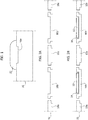
Figure 1 is a cross-sectional view of an electrically-conductive formation with lateral Cu growth; -
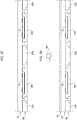
Figure 2A to 2J are exemplary of possible acts or steps in embodiments; -
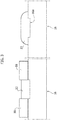
Figure 3 is a cross-sectional view of an electrically-conductive formation in one or more embodiments. - It will be appreciated that for the sake of clarity and ease of understanding the various figures may not be drawn to a same scale.
- In the ensuing description, various specific details are illustrated in order to provide an in-depth understanding of various examples of embodiments according to the description. The embodiments may be obtained without one or more of the specific details, or with other methods, components, materials, etc. In other cases, known structures, materials, or operations are not illustrated or described in detail so that various aspects of the embodiments will not be obscured.
- Reference to "an embodiment" or "one embodiment" in the framework of the present description is intended to indicate that a particular configuration, structure, or characteristic described in relation to the embodiment is comprised in at least one embodiment. Hence, phrases such as "in an embodiment", "in one embodiment", or the like, that may be present in various points of the present description do not necessarily refer exactly to one and the same embodiment. Furthermore, particular conformations, structures, or characteristics may be combined in any adequate way in one or more embodiments.
- The headings/references used herein are provided merely for convenience and hence do not define the extent of protection or the scope of the embodiments.
- In semiconductor device manufacturing, electrical connection between leadframes or substrates and semiconductor chips or dice arranged thereon can be provided in the form of metal wiring (so-called wire-bonding technology may be exemplary of such an approach).
- An insulating compound (an epoxy molding compound, for instance) can be molded onto a leadframe or substrate to encapsulate a semiconductor die or dice arranged thereon.
- Recent developments in that area (as witnessed by documents such as
US 2018/342433 A1 ,US 2018/342453 A1 orUS 2019/115287 A1 , for instance) disclose the possibility of using for that purpose an additivated molding compound, e.g. laser direct structuring (LDS) material. - Laser direct structuring (LDS) is a laser-based machining technique now widely used in various sectors of the industrial and consumer electronics markets, for instance for high-performance antenna integration, where an antenna design can be directly formed onto a molded plastic part. In an exemplary process, the molded parts can be produced with commercially available resins which include additives suitable for the LDS process; a broad range of resins such as polymer resins like PC, PC/ABS, ABS, LCP are currently available for that purpose.
- In LDS, a laser beam can be used to transfer a desired electrically-conductive pattern onto a plastic molding which may then be subjected to metallization (for instance via electroless plating with copper or other metals) to finalize a desired conductive pattern.
- For instance, once electrically-conductive formations, such as lines or vias, are structured in an LDS material "activated" via a laser beam, electrical conductivity of these formation can be facilitated by forming electrically-conductive material thereon. This may involve, for instance, forming a thin film by immersion into a copper (Cu) electroless bath, followed by galvanic Cu growth, this resulting in thick Cu tracks formed which connect the semiconductor die or dice and the leads.
- Direct copper interconnection has been regarded as hardly applicable to devices with fine pitch, that is with reduced spacing between adjacent electrically-conductive formations. Galvanic Cu growth is essentially isotropic and may thus imply lateral Cu growth over the electrically-conductive formations.
- This is exemplified in
Figure 1 wherereference numeral 16 denotes a substrate having arecessed portion 16a formed therein. This may be the case of a substrate of an LDS material exposed to laser beam activation energy to structure therein an electrically-conductive formation (a conductive line, for instance) at 16a.Reference 22 denotes an electrically-conductive (e.g. Cu) track or trace formed at 16a as discussed previously, and thus exhibiting some sort of lateral growth. - Such lateral growth places a constraint on the gap between adjacent conductive formations: in fact, too close spacing may lead to undesired contact (short circuit) between adjacent formations.
- Consequently, applying conventional LDS technology as discussed so far to provide such formations (tracks or vias, for instance) involves designing such formations with a separation (pitch) wide enough to facilitate avoiding undesired contact between adjacent formations after Cu plating.
- For instance (of course these figures are purely exemplary and non-mandatory) a conductive track having a width of 80 µm (resulting from laser beam activation of the LDS material) may eventually become 180 µm wide as a result of a 50 µm Cu lateral growth at each side of a track having 50 µm Cu plating growth.
- Conventional LDS technology as discussed so far is thus hardly applicable to "fine pitch" tracks or traces as desirable in application such as, for instance, smart power silicon technology, e.g., with 20 µm (minimum) laser spot and thick Cu plating.
- It is also observed that conventional LDS technology as discussed so far may lead to Cu spikes formed at corners or at vias due to uneven current density.
- One or more embodiments may facilitate preventing lateral Cu growth over electrically-conductive formations.
- In one or more embodiments, Cu tracks resulting from Cu growth over electrically-conductive formations may have substantially vertical edges.
-
Figures 2A to 2J are exemplary of various acts which may be implemented in fabricatingsemiconductor products 100. -
Figure 2A is exemplary of the provision of leadframe material 10 (Cu sheet, for instance). - The designation "leadframe" (or "lead frame") is currently used (see, for instance the USPC Consolidated Glossary of the United States Patent and Trademark Office) to indicate a metal frame which provides support for an integrated circuit chip or die as well as electrical leads to interconnect the integrated circuit in the die or chip to other electrical components or contacts.
- Essentially, a leadframe comprises an array of electrically-conductive formations (leads) 10a which from an outline location extend inwardly in the direction of a semiconductor chip or die thus forming an array of electrically-conductive formations from a
die pad 10b. - As conventional in the art, such a
leadframe 10 may be provided in the form of a strip of notionally indefinite length where a plurality of devices is formed, with the individual devices thus formed finally separated by a final "singulation" act. - To that effect the
leadframe 10 may be provided along its length with fiducials, not visible in the figure for simplicity. -
Figure 2B is exemplary ofsemiconductor dice 12 being attached onto thedie pads 10b in theleadframe 10. This may be via die attach adhesive 14 (DAF or standard glue dispensing, for instance), which is not expressly indicated with a reference symbol in the subsequent figures for clarity of illustration. -
Figure 2C is exemplary of LDSmolding compound 16 being molded onto the surface resulting from the act ofFigure 2B . - In one or more embodiments, the LDS
molding compound 16 may provide a (per se electrically-insulating) encapsulation of thesemiconductor die 12, possibly extending into the spaces between theleads 10a and thedie pad 10b in theleadframe 10. - As discussed, an LDS compound as 16 may comprise any of a broad range of LDS materials, for instance resin such as polymer thermoplastic resins like polycarbonate (PC), polycarbonate/acrylonitrile butadiene styrene (PC/ABS), acrylonitrile butadiene styrene (ABS), liquid-crystal polymer (LCP) and thermoset epoxy resins are currently available for that purpose.
-
Figure 2D is exemplary of a layer of resistmaterial 18 being formed (deposited, for instance) onto theLDS material 16. - Use of such resist materials is conventional in the area of manufacturing semiconductor devices such as integrated circuits, which makes it unnecessary to provide a more detailed description herein.
- Briefly, the designation resist applies to a layer of material which can be used to transfer a desired circuit pattern onto a substrate. Such a layer can be patterned in various ways to form a mask intended to protect certain regions of the substrate during subsequent processing steps.
- In one or more embodiments as exemplified herein, the (continuous)
layer 18 includes resist material which can be hardened by resorting to light exposure (from a source designated UV inFigure 2D ) after being formed onto theLDS material 16. - In one or more embodiments, the layer of resist
material 18 may be selected out of solder resist, epoxy material, adhesive tape and photoresist material: those of skill in the art will otherwise easily appreciate that these are merely exemplary, non mandatory options. - DuPont Riston 200 Series is exemplary of resist material which may be advantageously used in one or more embodiments.
-
Figure 2E is exemplary of electrically-conductive formations structured in theLDS material 16 with "activation" laser beam energy applied as exemplified by L. - As exemplified herein, such electrically-conductive formations comprise lines or traces 20a at the surface of the
compound 16 andvias 20b extending through thecompound 16 between opposed surfaces of the compound layer. - In one or more embodiments as exemplified herein, lines or traces 20a and
vias 20b are structured by laser beam energy traversing the resistlayer 18. - For instance, this may involve the (at least partial) evaporation or ablation of the layer of resist
material 18 under the action of the laser beam energy. - In one or more embodiments as exemplified herein, such laser beam etching of the layer of resist
material 18 will result in trenches (slits or grooves) or holes being formed in the resistmaterial 18 which are self-aligned with the lines/vias structured in theLDS material 16. -
Figure 2F is exemplary of metallization via Cu electroplating oflines 20a and/orvias 20b to facilitate their electrical conductivity. - In one or more embodiments, the thickness of the formed Cu layer may be 50 to 70 µm.
- As exemplified in
Figure 3 , the (self)alignment of: - the side walls of trenches (slits or grooves) or holes formed by the action of laser beam (as exemplified at L in
Figure 2E ) in the resistmaterial 18, - the lines/vias structured in the
LDS material compound 16 resulting from the act ofFigure 2E , - facilitates preventing Cu growth laterally of
lines 20a and/orvias 20b, so that electrically-conductive formations (Cu formations) 22 with substantially vertical edges are obtained. - This result is highlighted on the left-hand side of
Figure 3 by way of direct comparison with the conventional solution ofFigure 1 , which is once again reproduced on the right-hand side ofFigure 3 . - The representation on the left-hand side of
Figure 3 also shows that, in one or more embodiments, the electrically-conductive formations 22 may end up by having a front (upper) surface which is substantially level with the surface of the resist layer 18 (with no growth - also - over the resist surface). - This may facilitate forming electrically-
conductive formations 22 which fill the volume formed in the resistlayer 18, thus having a thickness which may reach up to the height/depth of the trenches or holes formed by the action of laser beam. -
Figure 2G is exemplary of possible (non-mandatory) removal of the layer of resistmaterial 18, which can be performed with any process known to those of skill in the art for that purpose. -
Figure 2H is exemplary of possible further steps in completing the packaging of the product 100 (possibly after resist removal as exemplified inFigure 2G ) . - For instance, the layer designated 24 in
Figure 2H may be exemplary of (further) package molding compound molded onto the assembly ofFigure 2F (possibly after resist removal as exemplified inFigure 2G ). In one or more embodiments, the (further) mass ofpackage molding compound 24 may include conventional (that is, non-LDS) molding compound such as an epoxy molding compound (EMC) . - The layer designated 24 in
Figure 2H may be likewise exemplary of stencil printing of solder coat (around 100 µm thickness, for instance) onto the assembly ofFigure 2F (again possibly after resist removal as exemplified inFigure 2G ). -
Figure 2I is exemplary of possible metal plating (tin plating, for instance) 10c formed at the bottom (back) surface of theleadframe 10. -
Figure 2J is exemplary of an act of singulation via a conventional singulation tool as exemplified at TS to formindividual semiconductor devices 100. - A method as exemplified herein may comprise:
- molding laser direct structuring material (for instance, 16) onto at least one semiconductor die (for instance, 12) to provide at least partial encapsulation thereof,
- forming resist material (for instance, 18) on the laser direct structuring material,
- applying laser beam energy (for instance, L) to the laser direct structuring material through the resist material formed thereon, wherein said laser beam energy produces mutually aligned patterns of electrically-conductive formations (for
instance - forming electrically-conductive material (for instance, 22) on said electrically-conductive formations structured in the laser direct structuring material at said etched-out portions of the resist material, wherein said electrically-conductive material has lateral confinement surfaces at said lateral walls of said etched-out portions of the resist material.
- In a method as exemplified herein, forming electrically-conductive material on said electrically-conductive formations structured in the laser direct structuring material may comprise growing electrically-conductive material at said etched-out portions of the resist material.
- In a method as exemplified herein, growing electrically-conductive material at said etched-out portions of the resist material may comprise immersing the laser direct structuring material and the resist material formed thereon having mutually aligned patterns of electrically-conductive formations and etched-out portions in a metal-containing bath.
- In a method as exemplified herein, growing electrically-conductive material at said etched-out portions of the resist material may comprise:
- growing a first, thin layer of electrically-conductive material on said electrically-conductive formations structured in the laser direct structuring material,
- growing a second, thick layer of electrically-conductive material on said first, thin layer of electrically-conductive material.
- A method as exemplified herein may comprise:
- growing said first layer of electrically-conductive material via an electroless bath, and
- growing said second layer of electrically-conductive material via galvanic growth.
- In a method as exemplified herein, said electrically-conductive material formed on said electrically-conductive formations structured in the laser direct structuring material may comprise copper.
- In a method as exemplified herein, said resist material may be selected out of solder resist, epoxy material, adhesive tape and photoresist material.
- In a method as exemplified herein, said electrically-conductive formations structured in the laser direct structuring material may comprise:
- electrically-conductive lines (for instance, 20a) over the laser direct structuring material, and/or
- electrically-conductive vias (for instance, 20b) through the laser direct structuring material.
- A method as exemplified herein may comprise removing said resist material formed on the laser direct structuring material subsequent to forming said electrically-conductive material on said electrically-conductive formations structured in the laser direct structuring material at said etched-out portions of the resist material.
- A device (for instance, 100) as exemplified herein may comprise:
- laser direct structuring material molded onto at least one semiconductor die to provide at least partial encapsulation thereof,
- a pattern of laser-beam activated, electrically-conductive formations structured in the laser direct structuring material, and
- electrically-conductive material formed on said electrically-conductive formations structured in the laser direct structuring material, wherein said electrically-conductive material formed on said electrically-conductive formations has lateral confinement surfaces aligned with said pattern of laser-beam activated, electrically-conductive formations in the absence of lateral growth with respect thereto.
- Without prejudice to the underlying principles, the details and the embodiments may vary, even significantly, with respect to what has been described by way of example only without departing from the scope of the embodiments.
- The extent of protection is determined by the annexed claims.
Claims (10)
- A method, comprising:molding laser direct structuring material (16) onto at least one semiconductor die (12) to provide at least partial encapsulation thereof,forming resist material (18) on the laser direct structuring material (16),applying laser beam energy (L) to the laser direct structuring material (16) through the resist material (18) formed thereon, wherein said laser beam energy (L) produces mutually aligned patterns of electrically-conductive formations (20a, 20b) structured in the laser direct structuring material (16) and etched-out portions of the resist material (18), said etched-out portions of the resist material (18) leaving said electrically-conductive formations (20a, 20b) uncovered and having lateral walls sidewise of said electrically-conductive formations (20a, 20b), andforming electrically-conductive material (22) on said electrically-conductive formations (20a, 20b) structured in the laser direct structuring material (16) at said etched-out portions of the resist material (18), wherein said electrically-conductive material (22) has lateral confinement surfaces at said lateral walls of said etched-out portions of the resist material (18).
- The method of claim 1, wherein forming electrically-conductive material (22) on said electrically-conductive formations (20a, 20b) structured in the laser direct structuring material (16) comprises growing electrically-conductive material (22) at said etched-out portions of the resist material (18) .
- The method of claim 2, wherein growing electrically-conductive material (22) at said etched-out portions of the resist material (18) comprises immersing the laser direct structuring material (16) and the resist material (18) formed thereon having mutually aligned patterns of electrically-conductive formations (20a, 20b) and etched-out portions in a metal-containing bath.
- The method of claim 2 or claim 3, wherein growing electrically-conductive material (22) at said etched-out portions of the resist material (18) comprises:growing a first, thin layer of electrically-conductive material on said electrically-conductive formations (20a, 20b) structured in the laser direct structuring material (16),growing a second, thick layer of electrically-conductive material on said first, thin layer of electrically-conductive material.
- The method of claim 4, comprising:growing said first layer of electrically-conductive material via an electroless bath, andgrowing said second layer of electrically-conductive material via galvanic growth.
- The method of any of the previous claims, wherein said electrically-conductive material (22) formed on said electrically-conductive formations (20a, 20b) structured in the laser direct structuring material (16) comprises copper.
- The method of any of the previous claims, wherein said resist material (18) is selected out of solder resist, epoxy material, adhesive tape and photoresist material.
- The method of any of the previous claims, wherein said electrically-conductive formations (20a, 20b) structured in the laser direct structuring material (16) comprise:electrically-conductive lines (20a) over the laser direct structuring material (16), and/orelectrically-conductive vias (20b) through the laser direct structuring material (16).
- The method of any of the previous claims, comprising removing said resist material (18) formed on the laser direct structuring material (16) subsequent to forming said electrically-conductive material (22) on said electrically-conductive formations (20a, 20b) structured in the laser direct structuring material (16) at said etched-out portions of the resist material (18) .
- A device (100), comprising:laser direct structuring material (16) molded onto at least one semiconductor die (12) to provide at least partial encapsulation thereof,a pattern of laser-beam activated, electrically-conductive formations (20a, 20b) structured in the laser direct structuring material (16), andelectrically-conductive material (22) formed on said electrically-conductive formations (20a, 20b) structured in the laser direct structuring material (16), wherein said electrically-conductive material (22) formed on said electrically-conductive formations (20a, 20b) has lateral confinement surfaces aligned with said pattern of laser-beam activated, electrically-conductive formations (20a, 20b) in the absence of lateral growth.
Applications Claiming Priority (1)
| Application Number | Priority Date | Filing Date | Title |
|---|---|---|---|
| IT202000006223 | 2020-03-24 |
Publications (1)
| Publication Number | Publication Date |
|---|---|
| EP3886147A1 true EP3886147A1 (en) | 2021-09-29 |
Family
ID=70739130
Family Applications (1)
| Application Number | Title | Priority Date | Filing Date |
|---|---|---|---|
| EP21163789.7A Withdrawn EP3886147A1 (en) | 2020-03-24 | 2021-03-19 | Method of manufacturing semiconductor devices and corresponding device |
Country Status (2)
| Country | Link |
|---|---|
| US (1) | US11626379B2 (en) |
| EP (1) | EP3886147A1 (en) |
Cited By (1)
| Publication number | Priority date | Publication date | Assignee | Title |
|---|---|---|---|---|
| EP4177936A1 (en) * | 2021-11-03 | 2023-05-10 | Nexperia B.V. | Semiconductor package and method for producing the same |
Families Citing this family (6)
| Publication number | Priority date | Publication date | Assignee | Title |
|---|---|---|---|---|
| US11887959B2 (en) * | 2020-12-17 | 2024-01-30 | Stmicroelectronics S.R.L. | Chip-on-lead semiconductor device, and corresponding method of manufacturing chip-on-lead semiconductor devices |
| US20220238473A1 (en) * | 2021-01-25 | 2022-07-28 | Stmicroelectronics S.R.L. | Method of manufacturing semiconductor devices and corresponding semiconductor device |
| TWI813139B (en) * | 2022-01-21 | 2023-08-21 | 強茂股份有限公司 | Semiconductor package element capable of improving side solderability and manufacturing method thereof |
| IT202300020505A1 (en) | 2023-10-04 | 2025-04-04 | St Microelectronics Int Nv | PROCEDURE FOR MANUFACTURING SEMICONDUCTOR DEVICES AND CORRESPONDING DEVICE |
| IT202400004246A1 (en) | 2024-02-28 | 2025-08-28 | St Microelectronics Int Nv | PROCEDURE FOR MANUFACTURING SEMICONDUCTOR DEVICES AND CORRESPONDING DEVICE |
| IT202400004300A1 (en) | 2024-02-28 | 2025-08-28 | St Microelectronics Int Nv | PROCEDURE FOR MANUFACTURING SEMICONDUCTOR DEVICES AND CORRESPONDING SEMICONDUCTOR DEVICE |
Citations (6)
| Publication number | Priority date | Publication date | Assignee | Title |
|---|---|---|---|---|
| GB2313713A (en) * | 1996-05-31 | 1997-12-03 | Nec Corp | High-density mounting method for and structure of electronic circuit board |
| US20020102745A1 (en) * | 2000-08-03 | 2002-08-01 | Institute Of Materials Research & Engineering | Process for modifying chip assembly substrates |
| JP2009081208A (en) * | 2007-09-25 | 2009-04-16 | Panasonic Electric Works Co Ltd | Method for manufacturing printed wiring board |
| US20180342453A1 (en) | 2017-05-23 | 2018-11-29 | Stmicroelectronics S.R.L. | Method of manufacturing semiconductor devices and corresponding product |
| US20180342433A1 (en) | 2017-05-23 | 2018-11-29 | Stmicroelectronics S.R.L. | Method of manufacturing semiconductor devices, corresponding device and circuit |
| US20190115287A1 (en) | 2017-10-12 | 2019-04-18 | Stmicroelectronics S.R.L. | Method of manufacturing semiconductor devices, corresponding device and circuit |
Family Cites Families (13)
| Publication number | Priority date | Publication date | Assignee | Title |
|---|---|---|---|---|
| JP5336711B2 (en) | 2007-07-09 | 2013-11-06 | セイコーインスツル株式会社 | Resin-sealed semiconductor device |
| US9202769B2 (en) | 2009-11-25 | 2015-12-01 | Stats Chippac, Ltd. | Semiconductor device and method of forming thermal lid for balancing warpage and thermal management |
| KR20120053386A (en) | 2010-11-17 | 2012-05-25 | 삼성전기주식회사 | Lead pin for package substrate and package substrate using the same |
| EP3017015A4 (en) | 2013-07-04 | 2017-07-05 | Melior Innovations Inc. | High strength low density synthetic proppants for hydraulically fracturing and recovering hydrocarbons |
| US20160100256A1 (en) | 2013-10-30 | 2016-04-07 | Knowles Electronics, Llc | Acoustic Assembly and Method of Manufacturing The Same |
| US9330994B2 (en) | 2014-03-28 | 2016-05-03 | Stats Chippac, Ltd. | Semiconductor device and method of forming RDL and vertical interconnect by laser direct structuring |
| JP6031059B2 (en) | 2014-03-31 | 2016-11-24 | 信越化学工業株式会社 | Semiconductor device, stacked semiconductor device, post-sealing stacked semiconductor device, and manufacturing method thereof |
| US9171739B1 (en) | 2014-06-24 | 2015-10-27 | Stats Chippac Ltd. | Integrated circuit packaging system with coreless substrate and method of manufacture thereof |
| US20170367182A1 (en) | 2014-12-12 | 2017-12-21 | Sabic Global Technologies B.V. | Laser direct structured materials and their methods of making |
| US9578744B2 (en) * | 2014-12-22 | 2017-02-21 | Stmicroelectronics, Inc. | Leadframe package with pre-applied filler material |
| US10037948B2 (en) * | 2016-08-19 | 2018-07-31 | Apple Inc. | Invisible compartment shielding |
| US20200161206A1 (en) * | 2018-11-20 | 2020-05-21 | Advanced Semiconductor Engineering, Inc. | Semiconductor package structure and semiconductor manufacturing process |
| US20200185293A1 (en) * | 2018-12-07 | 2020-06-11 | Infineon Technologies Ag | Semiconductor Package Having a Laser-Activatable Mold Compound |
-
2021
- 2021-03-11 US US17/199,340 patent/US11626379B2/en active Active
- 2021-03-19 EP EP21163789.7A patent/EP3886147A1/en not_active Withdrawn
Patent Citations (6)
| Publication number | Priority date | Publication date | Assignee | Title |
|---|---|---|---|---|
| GB2313713A (en) * | 1996-05-31 | 1997-12-03 | Nec Corp | High-density mounting method for and structure of electronic circuit board |
| US20020102745A1 (en) * | 2000-08-03 | 2002-08-01 | Institute Of Materials Research & Engineering | Process for modifying chip assembly substrates |
| JP2009081208A (en) * | 2007-09-25 | 2009-04-16 | Panasonic Electric Works Co Ltd | Method for manufacturing printed wiring board |
| US20180342453A1 (en) | 2017-05-23 | 2018-11-29 | Stmicroelectronics S.R.L. | Method of manufacturing semiconductor devices and corresponding product |
| US20180342433A1 (en) | 2017-05-23 | 2018-11-29 | Stmicroelectronics S.R.L. | Method of manufacturing semiconductor devices, corresponding device and circuit |
| US20190115287A1 (en) | 2017-10-12 | 2019-04-18 | Stmicroelectronics S.R.L. | Method of manufacturing semiconductor devices, corresponding device and circuit |
Cited By (1)
| Publication number | Priority date | Publication date | Assignee | Title |
|---|---|---|---|---|
| EP4177936A1 (en) * | 2021-11-03 | 2023-05-10 | Nexperia B.V. | Semiconductor package and method for producing the same |
Also Published As
| Publication number | Publication date |
|---|---|
| US20210305191A1 (en) | 2021-09-30 |
| US11626379B2 (en) | 2023-04-11 |
Similar Documents
| Publication | Publication Date | Title |
|---|---|---|
| US11626379B2 (en) | Method of manufacturing semiconductor devices and corresponding semiconductor device | |
| EP3719834B1 (en) | A method of manufacturing leadframes for semiconductor devices | |
| CN213583700U (en) | Semiconductor device with a plurality of transistors | |
| US11133242B2 (en) | Method of manufacturing semiconductor devices, corresponding device and circuit | |
| US5973388A (en) | Leadframe, method of manufacturing a leadframe, and method of packaging an electronic component utilizing the leadframe | |
| US20190378774A1 (en) | Method of manufacturing semiconductor devices and corresponding semiconductor device | |
| CN114361125A (en) | Semiconductor device and method for manufacturing semiconductor device | |
| US12500148B2 (en) | Method of coupling semiconductor dice, tool for use therein and corresponding semiconductor device | |
| EP4181177A1 (en) | Method of manufacturing semiconductor devices and corresponding semiconductor device | |
| EP4099368A1 (en) | Method of manufacturing semiconductor devices and corresponding semiconductor device | |
| JP3455685B2 (en) | Method for manufacturing semiconductor device | |
| US20230230948A1 (en) | Method of manufacturing semiconductor devices and corresponding semiconductor device | |
| US12463167B2 (en) | Method of manufacturing semiconductor devices and corresponding semiconductor device | |
| US20250167058A1 (en) | Enhanched thermal dissipation in flip-chip semiconductor devices using laser direct (lds) structuring technology | |
| US20250015038A1 (en) | Method of manufacturing semiconductor devices and corresponding semiconductor device | |
| US20240332143A1 (en) | Hybrid quad flat no-leads (qfn) integrated circuit package | |
| US20230360928A1 (en) | Method for manufacturing semiconductor devices and corresponding semiconductor device | |
| US20230005803A1 (en) | Method of manufacturing semiconductor devices and corresponding semiconductor device | |
| CN117012651A (en) | Method for manufacturing semiconductor device and corresponding semiconductor device | |
| US6875637B2 (en) | Semiconductor package insulation film and manufacturing method thereof | |
| US6894374B2 (en) | Semiconductor package insulation film and manufacturing method thereof | |
| US20250372488A1 (en) | Method of manufacturing semiconductor devices and corresponding semiconductor device | |
| US20240145429A1 (en) | Method of manufacturing semiconductor devices, corresponding leadframe, mold and semiconductor device | |
| US20250273623A1 (en) | Method of manufacturing semiconductor devices and corresponding device | |
| US20220199477A1 (en) | Method of manufacturing semiconductor devices and corresponding semiconductor device |
Legal Events
| Date | Code | Title | Description |
|---|---|---|---|
| PUAI | Public reference made under article 153(3) epc to a published international application that has entered the european phase |
Free format text: ORIGINAL CODE: 0009012 |
|
| STAA | Information on the status of an ep patent application or granted ep patent |
Free format text: STATUS: THE APPLICATION HAS BEEN PUBLISHED |
|
| AK | Designated contracting states |
Kind code of ref document: A1 Designated state(s): AL AT BE BG CH CY CZ DE DK EE ES FI FR GB GR HR HU IE IS IT LI LT LU LV MC MK MT NL NO PL PT RO RS SE SI SK SM TR |
|
| STAA | Information on the status of an ep patent application or granted ep patent |
Free format text: STATUS: THE APPLICATION IS DEEMED TO BE WITHDRAWN |
|
| 18D | Application deemed to be withdrawn |
Effective date: 20220330 |