EP3884531B1 - Hall integrated circuit and corresponding method of manufacturing of a hall integrated circuit using wafer stacking - Google Patents
Hall integrated circuit and corresponding method of manufacturing of a hall integrated circuit using wafer stacking Download PDFInfo
- Publication number
- EP3884531B1 EP3884531B1 EP19808646.4A EP19808646A EP3884531B1 EP 3884531 B1 EP3884531 B1 EP 3884531B1 EP 19808646 A EP19808646 A EP 19808646A EP 3884531 B1 EP3884531 B1 EP 3884531B1
- Authority
- EP
- European Patent Office
- Prior art keywords
- hall
- wafer
- layer
- sensor layer
- silicon
- Prior art date
- Legal status (The legal status is an assumption and is not a legal conclusion. Google has not performed a legal analysis and makes no representation as to the accuracy of the status listed.)
- Active
Links
Images










Classifications
-
- H—ELECTRICITY
- H10—SEMICONDUCTOR DEVICES; ELECTRIC SOLID-STATE DEVICES NOT OTHERWISE PROVIDED FOR
- H10B—ELECTRONIC MEMORY DEVICES
- H10B61/00—Magnetic memory devices, e.g. magnetoresistive RAM [MRAM] devices
-
- G—PHYSICS
- G01—MEASURING; TESTING
- G01R—MEASURING ELECTRIC VARIABLES; MEASURING MAGNETIC VARIABLES
- G01R33/00—Arrangements or instruments for measuring magnetic variables
- G01R33/02—Measuring direction or magnitude of magnetic fields or magnetic flux
- G01R33/06—Measuring direction or magnitude of magnetic fields or magnetic flux using galvano-magnetic devices
- G01R33/07—Hall effect devices
- G01R33/072—Constructional adaptation of the sensor to specific applications
-
- G—PHYSICS
- G01—MEASURING; TESTING
- G01R—MEASURING ELECTRIC VARIABLES; MEASURING MAGNETIC VARIABLES
- G01R33/00—Arrangements or instruments for measuring magnetic variables
- G01R33/02—Measuring direction or magnitude of magnetic fields or magnetic flux
- G01R33/06—Measuring direction or magnitude of magnetic fields or magnetic flux using galvano-magnetic devices
- G01R33/07—Hall effect devices
- G01R33/077—Vertical Hall-effect devices
-
- H—ELECTRICITY
- H10—SEMICONDUCTOR DEVICES; ELECTRIC SOLID-STATE DEVICES NOT OTHERWISE PROVIDED FOR
- H10N—ELECTRIC SOLID-STATE DEVICES NOT OTHERWISE PROVIDED FOR
- H10N52/00—Hall-effect devices
- H10N52/01—Manufacture or treatment
-
- H—ELECTRICITY
- H10—SEMICONDUCTOR DEVICES; ELECTRIC SOLID-STATE DEVICES NOT OTHERWISE PROVIDED FOR
- H10N—ELECTRIC SOLID-STATE DEVICES NOT OTHERWISE PROVIDED FOR
- H10N52/00—Hall-effect devices
- H10N52/101—Semiconductor Hall-effect devices
-
- H—ELECTRICITY
- H10—SEMICONDUCTOR DEVICES; ELECTRIC SOLID-STATE DEVICES NOT OTHERWISE PROVIDED FOR
- H10N—ELECTRIC SOLID-STATE DEVICES NOT OTHERWISE PROVIDED FOR
- H10N52/00—Hall-effect devices
- H10N52/80—Constructional details
-
- H—ELECTRICITY
- H10—SEMICONDUCTOR DEVICES; ELECTRIC SOLID-STATE DEVICES NOT OTHERWISE PROVIDED FOR
- H10N—ELECTRIC SOLID-STATE DEVICES NOT OTHERWISE PROVIDED FOR
- H10N59/00—Integrated devices, or assemblies of multiple devices, comprising at least one galvanomagnetic or Hall-effect element covered by groups H10N50/00 - H10N52/00
-
- H—ELECTRICITY
- H10—SEMICONDUCTOR DEVICES; ELECTRIC SOLID-STATE DEVICES NOT OTHERWISE PROVIDED FOR
- H10W—GENERIC PACKAGES, INTERCONNECTIONS, CONNECTORS OR OTHER CONSTRUCTIONAL DETAILS OF DEVICES COVERED BY CLASS H10
- H10W20/00—Interconnections in chips, wafers or substrates
- H10W20/01—Manufacture or treatment
- H10W20/021—Manufacture or treatment of interconnections within wafers or substrates
- H10W20/023—Manufacture or treatment of interconnections within wafers or substrates the interconnections being through-semiconductor vias
-
- H—ELECTRICITY
- H10—SEMICONDUCTOR DEVICES; ELECTRIC SOLID-STATE DEVICES NOT OTHERWISE PROVIDED FOR
- H10W—GENERIC PACKAGES, INTERCONNECTIONS, CONNECTORS OR OTHER CONSTRUCTIONAL DETAILS OF DEVICES COVERED BY CLASS H10
- H10W20/00—Interconnections in chips, wafers or substrates
- H10W20/01—Manufacture or treatment
- H10W20/031—Manufacture or treatment of conductive parts of the interconnections
- H10W20/056—Manufacture or treatment of conductive parts of the interconnections by filling conductive material into holes, grooves or trenches
-
- H—ELECTRICITY
- H10—SEMICONDUCTOR DEVICES; ELECTRIC SOLID-STATE DEVICES NOT OTHERWISE PROVIDED FOR
- H10W—GENERIC PACKAGES, INTERCONNECTIONS, CONNECTORS OR OTHER CONSTRUCTIONAL DETAILS OF DEVICES COVERED BY CLASS H10
- H10W20/00—Interconnections in chips, wafers or substrates
- H10W20/20—Interconnections within wafers or substrates, e.g. through-silicon vias [TSV]
-
- H—ELECTRICITY
- H10—SEMICONDUCTOR DEVICES; ELECTRIC SOLID-STATE DEVICES NOT OTHERWISE PROVIDED FOR
- H10W—GENERIC PACKAGES, INTERCONNECTIONS, CONNECTORS OR OTHER CONSTRUCTIONAL DETAILS OF DEVICES COVERED BY CLASS H10
- H10W90/00—Package configurations
Definitions
- the present invention relates to a Hall integrated circuit (IC) and to a corresponding method of manufacturing of a Hall integrated circuit using wafer stacking.
- IC Hall integrated circuit
- US 2014/0347045 specifies an isotropic three-dimensional Hall sensor with at least three electrode pairs wherein each electrode pair comprises a terminal on the front side and a terminal on the backside of a wafer.
- the three electrode pairs can be arranged such their directions through the wafer represent an orthogonal coordinate system.
- the Hall sensor region can be bounded laterally by deep trenches etched from both sides into the substrate.
- the electrical connections can be carried out by flip-chip or wire bonding.
- US 2006/0170406 specifies a vertical Hall element with three electrodes formed in a row on the primary surface of the substrate and one buried electrode established by an epi process.
- the three electrodes on the primary surface are surrounded by dielectric layers of predetermined depths by which current passage regions are defined.
- the buried electrode is electrically connected by a doped hook-up structure.
- WO 2010/101815 specifies a vertical Hall sensor with three electrodes formed in a well along a first axis.
- a fourth, buried electrode coupled to the well is formed by a deep diffusion region located below the well.
- the buried electrode is electrically connected by a doped hook-up structure.
- WO 2011/000601 specifies a vertical Hall sensor with a primary surface of the substrate, a Hall sensor region in contact with the primary surface and a buried conductive region in contact with the Hall sensor region.
- a vertical Hall sensor is disclosed having four electrodes on the primary surface and four buried electrodes. The buried electrodes are electrically connected by doped hook-up structures.
- US 2009/0256559 discloses a vertical Hall device which is formed on a substrate of first conductivity type having an epi layer of second conductivity type and buried conductive layer in between with second conductivity type.
- the vertical Hall device has four terminals. One terminal is connected to the conductive buried layer by a hook-up structure. There is an isolation structure between the hook-up structure and the other terminals.
- Magnetic sensor ICs typically use silicon-based Hall elements which are monolithically integrated with the electrical circuits required for signal conditioning and amplification.
- Typical commercial products with monolithically integrated Hall elements are Hall switch ICs, Hall ICs for linear position measurement, direct angle sensor Hall ICs, Hall ICs for current sensing and 3D Hall sensor ICs.
- a Hall IC may include horizontal Hall elements, vertical Hall elements, or both. Vertical Hall elements, which sense the strength of the magnetic field in a direction lying in the plane of the silicon surface, are used particularly in direct angle sensor Hall ICs and in 3D Hall sensor ICs.
- Conventional vertical Hall elements are formed as follows: A well having n-type conductivity is formed in the low-doped silicon substrate of p-type conductivity.
- the n-type well constitutes the Hall plate of the sensor being isolated from the substrate by a p-n junction. Then three, four, five or more Hall terminals are formed on the silicon surface within the region of the n-type well, typically arranged in a row or on a circle ( R. S. Popovic, "Hall Effect Devices", Institute of Physics Publishing, Bristol and Philadelphia 2004 ).
- conventional vertical Hall elements typically suffer from high residual offsets.
- the offset of a Hall element i.e. the Hall voltage measured at zero magnetic field strength, can be reduced by known techniques such as current spinning, orthogonal coupling of several Hall elements, or a combination thereof. Effective offset reduction relies on commutation of Hall terminals and on the four-fold symmetry of the Hall device.
- Single conventional vertical Hall elements having their terminals placed all on the same silicon surface deviate necessarily from an ideal four-fold symmetry.
- the object of the present invention is to satisfy the aforementioned need.
- a first wafer is provided, with an epitaxial semiconductor layer having a thickness for example in the range of 10 micrometers to 30 micrometers and having low doping of n-type conductivity.
- a first plurality of Hall terminals is formed on the first surface of the epitaxial semiconductor layer together with the corresponding wiring.
- a second wafer which is a silicon wafer having the typical dopant concentration and conductivity type used in CMOS manufacturing. Integrated circuits for signal conditioning and amplification of the Hall element are formed on first surface of the second wafer using standard CMOS manufacturing techniques.
- the first wafer is flipped and attached with its first surface onto the first surface of the second wafer, achieving a permanent wafer-to-wafer bonding.
- the stacked wafer is thinned from the second surface of the first wafer until only the low-doped semiconductor epitaxial layer with n-type conductivity remains.
- a second plurality of Hall terminals with corresponding wiring is formed on the thinned second surface of the first wafer applying identical design rules and process conditions as for the first set of Hall terminals. Hall terminals of the first plurality and Hall terminals of the second set are arranged on each surface such that the finished Hall element has four-fold symmetry.
- a deep trench isolation ring is formed extending through the entire epitaxial silicon layer and enclosing the first plurality of Hall terminals as well as the second plurality of Hall terminals. Electrical connections are provided such that each Hall terminal of the first plurality of Hall terminals and each Hall terminal of the second plurality of Hall terminals is individually connected to the wiring on the second wafer.
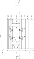
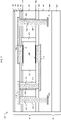
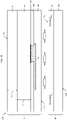
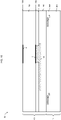
- FIG. 1 , FIG. 2 and FIG. 3 show the vertical Hall element 100 of an integrated Hall IC product.
- FIG. 1 shows the vertical Hall element 100 in the x-y-plane along the cut direction C-C' as indicated in FIG. 2 and FIG. 3 .
- FIG. 1 two further cut directions are indicated, the cut direction A-A' along the x-axis and the cut direction B-B' along the y-direction.
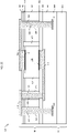
- FIG. 2 is a cross-sectional diagram displaying the vertical Hall element 100 in the x-z-plane along cut direction A-A'.
- FIG. 3 shows the same Hall element in the y-z-plane along the cut direction B-B' as indicated in FIG. 1 .
- the vertical Hall element 100 is formed on a first wafer 10, which is attached to second wafer 20, the latter comprising the integrated circuits for signal conditioning and amplification.
- a substrate 201 of the second wafer might be a low-doped silicon substrate having p-type conductivity; but is not limited to this. In general, any substrate that is suitable for manufacturing of CMOS devices and circuits could be selected.
- the CMOS devices and circuits which are formed on the substrate 201 of the second wafer 20 are not shown in FIG. 2 and FIG. 3 .
- 204 denotes the stack of dielectric layers formed on the substrate 201, in which the metal wirings of the circuits are embedded (according to standard CMOS processing techniques).
- the vertical Hall element of the Hall IC is formed on a substrate 102 of the first wafer 10.
- the substrate 102 might be a low-doped epitaxial silicon layer having n-type conductivity.
- the resistivity of the epitaxial silicon layer 102 is chosen such that vertical Hall element 100 has optimum characteristics, for example a high magnetic field sensitivity.
- the substrate 102 could be also a germanium substrate, a gallium arsenide (GaAs) substrate, a indium arsenide (InAs) substrate, an indium antimonide (InSb) substrate, or a substrate of a different material having optimal characteristics for the Hall element such as a high mobility.
- the substrate 102 is a low-doped epitaxial silicon layer having n-type conductivity (the reason for choosing n-type doping for silicon is the higher mobility, which translates into higher sensitivities values for the Hall sensor).
- Two shallow and highly doped regions 1 and 2 are formed having n-type conductivity and extending to a first surface 10b of the epitaxial silicon layer 102. As shown in FIG. 1 , the two highly doped regions 1 and 2 have a rectangular shape in the x-y plane, however, other shapes could be considered as well.
- the two highly doped regions 1 and 2 have a same width w and same length l. The distance between the two highly doped regions 1 and 2 is denoted by s.
- An oxide layer 104 is disposed on the first surface 10b having two openings, one located within the region of the highly doped region 1 and one located within the region of the highly doped region 2.
- 111 denotes a metal structure which comprises the metal filling of the opening in contact with the highly doped region 1 and a metal wire disposed on the oxide layer 104, which is in contact with said metal filling.
- 112 denotes a metal structure which comprises the metal filling of the opening in contact with the highly doped region 2 and a metal wire disposed on the oxide layer 104 being in contact with said metal filling.
- the wiring part of metal structure 111 extends in y-direction to the left side.
- An oxide layer 105 is disposed on the metal structures 111 and 112, as well as on the oxide layer 104, so that the wiring part of the metal structure 111 and the wiring part of the metal structure 112 are vertically embedded in oxide.
- the oxide layer 105 is planarized. With the planarized oxide surface the wafer 10 is attached and permanently bonded to the planarized oxide surface of layer 204 of wafer 20. Using the wafer 20 as carrier the wafer 10 has been thinned from backside such that only the epitaxial silicon layer 102 remains.
- the thickness of the epitaxial silicon remaining after the thinning is denoted by T3 (see Figure 5 ) and might be in the range of 10 micrometers to 30 micrometers, however, smaller or larger thickness values could be considered as well.
- the second surface of the epitaxial layer resulting after the thinning is denoted by 10d.
- 10b and 10d are two opposing surfaces of the epitaxial silicon layer 102, lying in the x-y-plane parallel to each other.
- Two shallow and highly doped regions 3 and 4 are formed having n-type conductivity and extending to the second surface 10d of the epitaxial silicon layer 102.
- the two highly doped regions 3 and 4 have the same width w and same length I as their counterparts 1 and 2.
- the two highly doped regions 3 and 4 are separated by the same distance s, by which the highly doped regions 1 and 2 are separated from each other.
- the highly doped region 3 is located directly above the highly doped region 2 in the sense that a straight line connecting the center of region 3 and the center of region 2 would be perpendicular to the epitaxial silicon surfaces 10b and 10d.
- the highly doped region 4 is located directly above the highly doped region 1 in the sense that a straight line connecting the center of region 4 and the center of region 1 would be perpendicular to the epitaxial silicon surfaces 10b and 10d.
- An oxide layer 106 is disposed on the second surface 10d of the epitaxial silicon layer and a silicon nitride layer 108 is disposed thereon.
- a deep trench isolation ring 107 is formed which extends from the second surface 10d to the first surface 10b.
- An inner surface of the deep trench isolation is perpendicular to the two surfaces 10b and 10d of the epitaxial silicon layer.
- the deep trench isolation ring 107 encloses the highly doped regions 1 and 2, which extend to the first surface 10b.
- the distance between the deep trench isolation ring 107 and the highly doped region 2 is denoted with d.
- the distance between the deep trench isolation ring 107 and highly doped region 1 in x-direction has the same value d.
- the epitaxial silicon volume enclosed by the deep trench isolation ring 107 (being separated and isolated from the remaining portion of the epitaxial silicon layer 102, external thereto) constitutes the Hall sensor region or Hall plate of the finished vertical Hall element 100 and is denoted by 103.
- the combined stack of layer 106 and 108 has two openings, one located within the highly doped region 3 and one located within the highly doped region 4.
- two metal structures 113 and 114 are formed.
- the metal structure 113 comprises the metal filling of the opening in contact with region 3 and a metal wiring disposed on the silicon nitride layer 108, the metal wiring being connected to said metal filling.
- the metal structure 114 comprises the metal filling of the opening in contact with region 4 and a metal wiring disposed on the silicon nitride layer 108, the metal wiring being in contact with said metal filling.
- the wiring part of metal structure 114 extends laterally to right side (along y-direction). Same is true also for the metal structure 113.
- An oxide layer 110 is disposed on the meta! structure 113 and 114 and on the silicon nitride layer 108.
- the wiring part of metal structures 113 and 114 are thus vertically embedded in dielectric material.
- a silicon nitride layer 132 is disposed on the oxide layer 110.
- the vertical Hall element depicted in FIG. 1 , FIG. 2 and FIG.3 has four Hall terminals. Each Hall terminal is associated with one of the four highly doped regions 1, 2, 3 and 4 formed in the epitaxial silicon layer 102. In the following, the Hall terminals are denoted by the same number as their associated highly doped regions.
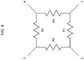
- a Hall element having four terminals can be represented by an equivalent circuit as shown in figure 4 .
- the four terminals 1, 2, 3 and 4 are connected via four resistances R1, R2, R3 and R4 (in a Wheatstone bridge). As is known in the art, an effective offset cancellation can be achieved, if the four resistances R1, R2, R3 and R4 have the same or nearly same value.
- the epitaxial silicon thickness T3, the width of the Hall terminals w, their lateral spacing s and the distance d to the deep trench isolation can be set such that the four resistances R1, R2, R3 and R4 are equal or nearly equal.
- the vertical Hall element has a four-fold symmetry or a nearly four-fold symmetry with respect to the four terminals (which may thus have corresponding geometrical and electrical properties).
- the doping concentration of the Hall sensor region 103 can be assumed to be homogeneous, since the doping is defined by the epitaxial growth of the layer 102.
- the inner surfaces of the deep trench isolations are perpendicular to the first and second surface of the epitaxial silicon layer.
- the vertical Hall element is sensitive to a magnetic field that is oriented in y-direction.
- the current direction is perpendicular or nearly perpendicular to a straight line connecting the two Hall terminals, between the Hall voltage is measured.
- This geometry allows high values of sensitivity to be obtained. Short-circuits effects, typically reducing the sensitivity in conventional vertical Hall elements, are minimized in the vertical Hall element 100.
- a large sensitivity for the vertical Hall element 100 can further be obtained, since the thickness T3 can be selected to be large, particularly, it can be selected far larger than the depth of the Hall plate of a conventional vertical Hall element.
- FIG. 7 is another cross-sectional diagram of the vertical Hall element 100 in cut direction B-B' along the y-direction, which shows in addition to FIG. 3 also the connections of the Hall terminals 1 and 4 to the integrated circuit of the Hall IC.
- the metal structure 111 in contact with Hall terminal 1 extends laterally to the left beyond the deep trench isolation 107. At the left end, the metal wire is formed as metal pad.
- a through silicon via 121 sitting on said metal pad provides an electrical connection between metal structure 111 to a metal bridge 115 formed above the second surface 10d of the epitaxial silicon layer.
- the through silicon via 121 extends through the combined stack of dielectric layers 106 and 108, through the epitaxial silicon layer 102 and through the oxide layer 104.
- the through silicon via 121 is filled with conductive material, the conductive filling being dielectrically isolated by an oxide liner 109 from the surrounding substrate 102.
- the metal bridge 115 entirely covers the through silicon via 121, which with it is in electrical contact.
- the metal bridge 115 further laterally extends to the left and covers here a second through silicon via, denoted by 141.
- the silicon through via 141 provides an electrical connection between the metal bridge 115 and landing pad 221 being embedded in the intermetal oxide layers 204 disposed on the substrate 201 of wafer 20.
- the through silicon via 141 extends through the combined stack of dielectric layers 106 and 108, through the epitaxial silicon layer 102, through the oxide layers 104 and 105, and through a portion of the oxide layer 204 disposed on the silicon substrate 201 of wafer 20.
- the through silicon via is filled with conductive material, the conductive filling being isolated from epitaxial silicon substrate 201 by the oxide liner 109.
- the landing pad 221 is connected to the wiring of the integrated circuits disposed on substrate 20.
- the metal structure 114 extends to the right beyond the deep trench isolation. It covers a further through silicon via 164 establishing an electrical contact to the conductive filling of the through silicon via.
- the through silicon via 164 extends through the combined stack of layer 106 and 108, through the entire epitaxial silicon layer 102, through the oxide layers 104 and 105, and through a portion of the intermetal oxide layers denoted by 204.
- the through silicon via 164 lands on a respective metal pad 224. In this way, an electrical connection between the Hall terminal 4 formed on the second surface 10d of the epitaxial silicon layer 102 and the wiring exiting on the IC wafer 20 is established.
- FIG. 8 is an aerial diagram showing the wiring and the vertical interconnections of the vertical Hall element 100 needed to access each of the four Hall terminals individually from the circuit wiring formed on wafer 20.
- Four metal pads denoted by 221, 222, 223 and 224 are embedded on the intermetal dielectric layer 204 of wafer 20 to provide access points to the four Hall terminals 1, 2, 3 and 4, respectively.
- the through silicon vias 141, 121, and 164, required to access the two Hall terminals 1 and 4, respectively, are arranged along a straight line parallel to the y-direction, which goes through the center of the Hall terminals 1. and 4.
- the distances of the through silicon vias to the Hall element are denoted by D4, D2, and D6 respectively.
- the through silicon vias 142, 122 and 163, required to access the Hall terminals 2 and 3, respectively, are arranged along the straight line parallel to the y-direction, which goes through the center of the Hall terminals 2 and 3.
- the through silicon vias 142, 122 and 163 have the same distances D4, D2 and D6 to the Hall terminals as the through silicon vias 141, 121 and 164, respectively.
- the wirings of the Hall terminals and the metal bridges are all oriented in y-direction.
- FIG. 8 the direction of the current flow through the wiring and vertical interconnections is indicated for first operation phase P1, in which a current is fed through the vertical Hall element from Hall terminal 3 to Hall terminal 1.
- first operation phase P1 in which a current is fed through the vertical Hall element from Hall terminal 3 to Hall terminal 1.
- the vertical current flow through the through silicon via 163 gives rise to an induced magnetic field, to which the vertical Hall element is sensitive.
- the vertical current flow through the through silicon via 121 gives rise to an induced magnetic field, to which the vertical Hall element is sensitive.
- the vertical current flow through the through silicon via 141 gives rise to an induced magnetic field, to which the vertical Hall element is sensitive.
- the current direction is same in the through silicon vias 121 and 163, their induced magnetic fields cancel in tendency at the location of vertical Hall element 100.
- the strengths of the induced magnetic fields at the vertical Hall element 100 depend on their distances D4, D2 and D6, respectively. Given the indicated current directions in the through silicon vias 141, 121 and 163, the distances D4, D2 and D6 can be set such that the parasitic magnetic field induced by the vertical current flow through the through silicon vias can be minimized at the location of the vertical Hall element. This holds true also for the other three operating phases of the vertical Hall element 100.
- the fabrication of the stacked Hall sensor 100 is depicted in the FIG. 9 to 30 .
- a wafer 10 comprising a silicon substrate 101 and an epitaxial layer 102.
- the substrate 101 is preferably a highly doped silicon substrate having n-type conductivity.
- the thickness T1 of the silicon substrate depends on the wafer size and might be in the range of 600 micrometers to 800 micrometers.
- the epitaxial layer 102 is preferably a lightly doped silicon epitaxial layer having n-type conductivity as well.
- the thickness T2 of the epitaxial layer might be in the range of 10 micrometers to 30 micrometers, however, lower or higher values for the thickness T2 can be considered as well.
- the resistivity of the silicon epitaxial layer is chosen such that optimum Hall sensor characteristics are obtained for the finished device.
- the optimum resistivity of the silicon epitaxial layer 102 depends on the thickness and the size of the Hall plate. Typical resistivities might be in the range of 0.1 ohm-cm and 10 ohm-cm. Other semiconductor materials could be considered as well for the epitaxial layer 102.
- the starting material could also a silicon-on-insulator wafer (SOI).
- SOI silicon-on-insulator wafer
- the epitaxial layer 102 is separated from the carrier substrate 101 by a buried oxide layer (BOX).
- BOX buried oxide layer
- the first surface of the wafer 10b which is defined by the low-doped epitaxial layer
- the rear surface of the wafer 10 is denoted by 10a.
- alignment marks are created on the surface 10b. This is accomplished by conducting a photo-masked etch into the silicon as is known by a skilled person. The alignment marks printed in silicon are used to align subsequent photo layers performed on surface 10b of wafer 10. The alignment marks are not shown in FIG. 9 .
- a shallow and highly doped region 1 is created by a photo-masked implantation followed by resist removal and laser thermal annealing.
- the highly doped region 1 has n-type conductivity and extends to the surface 10b.
- the doping concentration might be in the range of 10 20 atoms/cm 3 to 10 22 atoms/cm 3 .
- the wafer is subjected to very short heat pulses so that the heat can penetrate in the silicon only to a limited depth depending on the pulse time, energy dose and wavelength.
- the depth of the highly doped region might be in the range of 50 nanometers to 200 nanometers, which is far less than the thickness T2 of silicon epitaxial layer 102.
- an oxide layer 104 is deposited on the surface 10b.
- the oxide layer might be tetraethyl orthosilicate (TEOS) deposited by plasma enhanced chemical vapor deposition (PECVD).
- PECVD plasma enhanced chemical vapor deposition
- a contact trench or hole 151 is etched through the oxide layer 104 such that the highly doped region 1 becomes exposed. More precisely, the trench or hole 151 exposes the silicon epitaxial layer only within the highly doped region 1.
- the silicon consumption of such a photo-masked oxide etch can be quite low depending on the oxide-to-silicon selectivity of the etch chemistry and condition. In this way the etch can be stopped within the shallow highly doped region 1 ensuring that the doping concentration at the silicon surface inside of the trench or hole 151 is in the range of 10 20 atoms/cm 3 to 10 22 atoms/cm 3 .
- the fabrication of the Hall sensor continues with the deposition of a metal layer, which is structured by a photo-masked etching step as shown in FIG. 12 .
- the metal layer is preferably an aluminum-based metal stack typically comprising a titanium adhesion layer, a titanium nitride barrier layer, an aluminum layer and titanium nitride cap layer.
- the thickness of the titanium nitride barrier layer might be increased compared to a typical thickness. In any case, the inventors consider a thickness in the range of 500 angstrom to 1500 angstrom as suitable.
- the metal structure 111 fills the contact trench or hole 151 such that the metal is in contact with the exposed highly doped silicon inside of the trench or hole. Furthermore, the metal structure 111 extends to the right side in FIG. 12 forming a wire or pad on top of the oxide layer 104.
- metal structures are created on top of the oxide layer 104, which are provided as alignment marks for the processing of the wafer 10 on the second surface after its thinning as will become clearer in the following.
- the provided metal alignment structures are not shown in FIG. 12 .
- an oxide layer 105 is deposited on top of the metal structure 111 and the exposed oxide layer 104.
- the oxide layer 105 is planarized by chemical-mechanical polishing (CMP).
- CMP chemical-mechanical polishing
- 10c denotes the top surface of the oxide layer 105 after planarization. To achieve a good flatness of the oxide surface 10c, the steps of depositing an oxide layer and performing CMP might be repeated several times.
- a wafer 20 is provided consisting of a silicon substrate 201.
- 20b denotes the top or frontside surface of the wafer 20
- 20a denotes the rear surface.
- the substrate 201 has a p-type conductivity, which is the typical conductivity type used to form CMOS devices and circuits.
- the resistivity of the substrate 201 might be chosen to be suitable for the formation and the mutual isolation of CMOS devices.
- the thickness T4 of the wafer might be in the range of 600 micrometers to 800 micrometers.
- the required devices and circuits for the conditioning, read-out and signal amplification of the Hall sensor are formed on the substrate 201 in the typical fashion. To simplify matters these devices and circuits are not shown in FIG. 15 .
- the circuit wiring is embedded in oxide layers, which are as whole denoted by 204 in FIG. 15 .
- Two embedded metal pads, 221 and 224, preferably formed by the uppermost metal layer of the wiring, are provided for establishing contacts to the finished Hall sensor device being formed on the wafer 10.
- the uppermost metal layer might be an aluminum-based metal stack typically comprising a titanium adhesion layer, a titanium nitride barrier layer, an aluminum layer and titanium nitride cap layer. The thickness of the titanium nitride cap layer might be increased compared to a typical thickness.
- the inventors consider a thickness in the range of 500 angstrom to 1500 angstrom as suitable.
- the top surface of the oxide layer 204 is denoted by 20c.
- CMP chemical-mechanical polishing
- a sequence of oxide deposition and CMP steps could be performed to further improve the flatness of the oxide surface 20c. No bonding pads are provided on wafer 20 for external communication.
- the wafer 10 is flipped and attached with its surface 10c onto the surface 20c of wafer 20.
- a permanent bond is achieved between wafer 10 and wafer 20.
- the resulting stacked wafer is denoted by 30 in the following.
- the wafer 30 has surface 10a as top or front surface and surface 20a as rear surface.
- the planarized oxide surface 10c of wafer 10 is activated by a plasma with an inert gas.
- the planarized surface 20c of the wafer 20 is activated by a plasma with an inert gas.
- the bond alignment accuracy i.e. the alignment accuracy with which wafer 10 is attached on wafer 20
- the bond alignment accuracy is typically in the order of a few micrometers applying standard methods known in the art.
- a low temperature bake is performed to strengthen the bonding.
- the baking process may be in the range of lower than 450 °C, preferably lower than 400 °C. In theory, it is believed that the bonding relies on Van-der-Waals forces between the two oxide surfaces.
- adhesive bonding using polymer adhesives such as benzocyclobutene (BCB) or others may be used as well to achieve a reliable bonding between the wafer 10 and the wafer 20.
- BCB benzocyclobutene
- the Hall sensor wafer 10 is processed from its rear surface 10a. As shown in FIG. 17 , the wafer 10 is thinned from the rear side removing most of the silicon material. In particular, the initial substrate 101 of wafer 10 is completely removed and also the thickness of the epitaxial 102 is slightly reduced. The resulting thickness T3 of the epitaxial layer 102 is slightly lower than the initial thickness T2. The resulting epitaxial surface is denoted by 10d.
- the thinning process can include removal processes such as back grinding, chemical-mechanical polishing (CMP) and wet or dry etching. A preferred method is described in the following. The bulk of the substrate 101 is removed by back grinding.
- the back grinding is stopped before the epitaxial layer 102 becomes exposed.
- a wet etch is performed which is selective to the doping concentration of the silicon material. Since the substrate 101 is preferably selected to have a high doping concentration, the wet etch can selectively be stopped on the lightly doped silicon epitaxial layer owing to the large difference in the doping concentrations.
- a CMP process might be performed to further planarize and smoothen the resulting silicon surface. With this approach a good wafer-to-wafer control of the thickness T3 as well as a good within-wafer uniformity of T3 can be achieved.
- 10b has denoted the first silicon surface of the Hall sensor device. It has been shown how Hall terminals and accompanying wiring is formed on the first silicon surface by applying standard semiconductor processing methods with the only exception of the laser thermal annealing used for activation of the dopants.
- the fabrication of Hall sensor is continued by executing semiconductor manufacturing processes on the second surface 10d. To achieve a high degree of symmetry of the Hall sensor device, care is taken to apply identical design rules and process conditions for the formation of Hall terminals on the first and on second surface.
- another important aspect to achieve the desired symmetry is the accurate alignment of the Hall terminals formed on the second surface 10d to the Hall terminals formed on the first surface 10b.
- alignment patterns have been created on the first surface by structuring the deposited metal layer accordingly.
- silicon is removed by a photo-masked etch process in those regions, where the alignment patterns are conjectured. Due to the large size of the silicon openings required to catch the alignment patterns, these metal alignments patterns might be provided only at the edge of the wafer.
- the alignment accuracy that can be achieved by applying the described method, lies in the range of 100 nanometers to 500 nanometers.
- a new set of shot wise alignment patterns can be created on the second surface by a photo-masked etch into the epitaxial silicon, using the opened metal alignment patterns at wafer edge for alignment. In this way, the mutual alignment of the photo layers applied on the second surface 10d can be improved.
- a shallow and highly doped region 4 having n-type conductivity is formed on the second surface 10d in the identical fashion as the highly doped region 1 on the first surface.
- the same implant species, implant dose and energy are used as were used on the first surface to create the doping region 1.
- the same laser thermal annealing condition is applied after resist removal as was applied on the first surface for activating doping region 1.
- the aluminum-based metallization on the first surface of Hall sensor wafer 10 can be prevented from being ruined by heat treatment, in contrast to other activation methods such as furnace annealing or rapid thermal processing.
- the doped region 4 has the same lateral dimensions as the doped region 1. As indicated in FIG 18 , the doping region 4 is located directly above doping region 1. The two doping regions 1 and 4 are facing each other and are separated by the silicon epitaxial layer 102.
- the oxide layer 106 is deposited on the second surface 10d. More specifically, the layer 106 might be tetraethyl orthosilicate (TEOS) deposited by plasma enhanced chemical vapor deposition (PECVD). PECVD allows TEOS deposition at temperatures at or below 400 °C.
- PECVD plasma enhanced chemical vapor deposition
- a ring-shaped opening 161 is etched through the oxide layer 106 exposing the silicon epitaxial layer 102.
- the ring-shaped opening is formed around the Hall sensor device.
- the ring-shaped opening of the oxide layer 106 appears as two openings, which are located on left and on the right side of the highly doped region 4.
- a deep silicon etch is performed using the oxide layer 106 as hard mask, as depicted in FIG. 20 .
- the deep silicon etch is stopped selectively on the oxide layer 104 deposited on the first surface 10b of the Hall sensor wafer 10.
- a ring-shaped trench is created around the silicon region, in which the Hall terminals are formed.
- the enclosed silicon region will form the Hall plate of the finished Hall element and is denoted by 103.
- Deep silicon etching processes for etching trenches or vias having depths of several tens of micrometers or more are known in the art.
- a plasma etch process using a gas chemistry consisting of SF 6 , HBr and O 2 could be used.
- a so-called Bosch process could be applied, which typically is characterized by a better selectivity to the oxide hard mask.
- etching processes nearly vertical sidewalls are obtained as is known by a person skilled in the art.
- the ring-shaped trench 161 is filled by dielectric material, which is removed on top of oxide layer 106 by chemical-mechanical polishing.
- the dielectric material could be tetraethyl orthosilicate (TEOS), or a spin-on dielectric such as spin-on-glass (SOG), polyimide (PI) or benzocyclobutene (BCB).
- TEOS tetraethyl orthosilicate
- SOG spin-on-glass
- PI polyimide
- BCB benzocyclobutene
- the dielectric material is selected among dielectric materials that may be processed at temperatures not above 400 °C.
- the subsequent removal of dielectric material disposed on top of the oxide layer 106 by chemical-mechanical polishing is not selective to that oxide. The crucial point is only that the CMP process is stopped before silicon becomes exposed. After all, the Hall sensor region is confined dielectrically by deep trench isolation ring, in FIG. 21 denoted by 107.
- a silicon nitride layer 108 is deposited on top of the oxide layer 106 by PECVD as shown in FIG. 22 .
- the deposition temperature is not above 400 °C.
- the openings 171, 172 and 173 are etched through the stacked dielectric layer comprising the oxide layer 106 and the silicon nitride layer 108.
- the underlying silicon epitaxial layer is exposed.
- the photoresist is stripped.
- the opening 171 is located above the metal pad 221.
- the opening 171 is laterally enclosed by the metal pad 221, and the lateral enclosure of opening 171 by the metal pad 221 has a certain overlap margin, which is among others defined by the wafer bonding alignment accuracy.
- the opening 173 is located above the metal pad 224 and is enclosed laterally by said metal pad with the same overlap margin.
- the opening 172 is located above the metal structure 111. At this position, the metal structure is formed as a metal pad providing laterally an enclosure to the opening 172.
- the overlap margin of the metal pad enclosure with respect to the opening 172 is among others defined by the alignment accuracy achieved between the two active silicon surfaces 10d of 10b of the Hall sensor wafer 10.
- a deep silicon etch process is executed using the silicon nitride layer 108 as hard mask. As similar dry etching process as used for the definition of deep trench isolation 107 can be applied for this purpose. The deep silicon etch is stopped selectively on the oxide layer 104.
- a thin oxide layer 109 is deposited. More specifically, the layer 109 might be tetraethyl orthosilicate (TEOS) deposited by plasma enhanced chemical vapor deposition (PECVD) at a temperature not above 400 °C.
- TEOS tetraethyl orthosilicate
- PECVD plasma enhanced chemical vapor deposition
- the oxide layer 109 serves as a dielectric liner on the silicon sidewalls exposed by the preceding deep silicon etch.
- the thickness of the oxide layer 109 might be, to give an example, 3000 angstroms, but is not limited to this value.
- a further anisotropic dry etching process is executed using a process condition which suitable for etching oxide with high selectivity to silicon nitride and with high selectivity to titanium nitride.
- the thin oxide 109 is etched through at the bottom of the deep silicon vias 171, 172 and 173, as well as on the top above the silicon nitride layer 108. Owing to the high degree of anisotropy of such etching processes, the oxide layer 109 is kept almost entirely on the silicon sidewalls of the vias 171, 172 and 173. As etching is proceeded, the oxide layer 104, deposited on the first surface of wafer 10, is etched through as well.
- the dry etching stops selectively in the titanium nitride barrier layer of the metal structure 111.
- oxide-to-titanium nitride selectivity 20:1 to more than 40:1 can be obtained as is known in the art.
- the etch can be stopped within said titanium nitride layer and aluminum does not become exposed.
- Such etching processes typically show also a high selectivity to silicon nitride, so that in the present case the silicon nitride layer 108 is preserved to a large extent.
- the etch might stop somewhere in the oxide layer 105 depending on the applied etch time, as indicated in FIG. 25 .
- a photo step is performed with the result that at least the via 172 is filled and covered by photoresist and the vias 171 and 173 are not filled and covered by photoresist.
- photoresist coverage 195 is limited to the via 172 with some overlap around the via.
- a further dry oxide etching process is executed with high oxide-to-titanium nitride selectivity.
- the oxide layer 105 is etched through and as etching is continued, the metal pads 221 and 224 are reached, respectively.
- the etch can be stopped within said titanium nitride layer without the underlying aluminum becoming exposed. Since the via 172 is filled and covered by photoresist, no etching occurs at the bottom of this via. In the areas, which are not covered by photoresist, the silicon nitride layer 108 serves as hard mask. After completion of the oxide etching process, the photoresist 195 is stripped.
- a tantalum adhesion layer, an optional tantalum nitride barrier layer and a copper seed layer are deposited.
- the vias 171, 172 and 173 are filled with copper by electroplating. Owing to additives given to plating chemistry and by careful adjustment of the plating rate, the vias 171, 172, and 173 can be filled with copper without leaving voids or seams. Methods for filling through silicon vias of high aspect ratio with electroplated copper without voids or seams are known in the art.
- a copper CMP process is applied to remove copper plated on top of the silicon nitride layer 108.
- the tantalum and tantalum nitride deposited on top of the nitride layer 108 is completely removed.
- through silicon vias are formed, which are denoted by 141, 121, and 124, respectively.
- the through silicon vias are electrically isolated from the surrounding epitaxial silicon 102 by the oxide liner 109.
- the through silicon via 141 establishes an electrical connection to the wiring of the CMOS wafer 20.
- the through silicon via 124 establishes an electrical connection to the wiring of the CMOS wafer 20 by landing on the metal pad 224.
- a contact trench or hole 181 is formed by a photo-masked etching process through the silicon nitride layer 108 and through the oxide layer 106 such that the highly doped region 4 becomes exposed. More precisely, the trench or hole 181 exposes the silicon epitaxial layer only within the highly doped region 4. Thanks to the set of shot wise alignment patterns created on the second surface 10d, both, the photo process for the definition of the doped region 4 and the photo process for the definition of the opening 181, can be aligned to the same set of alignment patterns ensuring a high degree of mutual overlay accuracy.
- the etching can be stopped within the shallow highly doped region 4 ensuring that the doping concentration at the silicon surface inside of the trench or hole 181 is in the range of 10 20 atoms/cm 3 to 10 22 atoms/cm 3 .
- the photomask is stripped.
- a metal layer is deposited filling the contact trench or hole 181.
- the metal layer could be an aluminum-based metal stack comprising a tantalum adhesion layer, a tantalum nitride barrier layer, an aluminum layer and titanium nitride cap layer.
- the metal layer is structured by photo-masked etching process as shown in FIG. 29 .
- the metal structure 115 fully covers the top surface of the copper filled through silicon via 141 and top surface of the through silicon via 121, achieving an electrical connection between the two through silicon vias.
- the metal structure 114 comprises the filling of the contact trench or hole 181.
- the metal structure 114 extends to the right side passing over the deep trench isolation 107 and covering fully the top surface of the copper filled through silicon via 124.
- the metal structure 114 provides an electrical connection between the highly doped region 4 formed in the epitaxial silicon and the through silicon via 124.
- the structuring of the deposited aluminum-based metal stack is used also to form bonding or bumping pads for external communication of the finished wafer-stacked Hall IC product.
- the bonding or bumping pads are electrically connected to the wiring on the CMOS wafer 20 by through silicon vias like 141 or 124, which land on corresponding metal pads like 221 or 224, provided on wafer 20.
- an oxide layer 110 is deposited on top of the metal structures 115 and 114, and on the remaining silicon nitride layer 108. Then a silicon nitride layer 132 is deposited serving as passivation for the finished product. Both deposition steps are conducted at temperatures not above 400 °C using plasma enhanced physical vapor deposition. The oxide/silicon nitride stack is opened above the bonding or bumping pads by a photo-masked etching process, which is not shown in FIG. 29 .
- the proposed solution solves the problem of the low sensitivity of conventional vertical Hall elements integrated in Hall ICs.
- a high sensitivity can be achieved since the Hall terminals on the first surface and the Hall terminals on the second surface of the epitaxial semiconductor can be arranged such that in each phase of device operation the operating current flows vertically to a line connecting the two Hall terminals between which the Hall voltage is measured. In this way, short-circuit effects are minimized, which in conventional vertical Hall elements commonly reduce the sensitivity.
- a high sensitivity for the vertical Hall element can be achieved with the proposed solution also, because the thickness of the epitaxial semiconductor layer can be optimized towards a high sensitivity.
- the proposed technical solution allows to use an epitaxial semiconductor material other than silicon as Hall plate.
- the Hall sensitivity is proportional to the mobility of the majority carriers.
- the sensitivity can thus be further enhanced by selecting an optimized semiconductor material with high mobility. For instance, low-doped germanium with n-type conductivity could be selected as an alternative material.
- the vertical Hall element formed on the first wafer can be optimized with respect to sensitivity without modifying the semiconductor manufacturing processes, materials or design rules applied for the fabrication of the wafer containing the integrated circuits of the Hall IC.
- the proposed solution moreover solves the problem of high residual offset of conventional vertical Hall elements integrated in Hall ICs, since the vertical Hall element established on the first wafer can be designed and manufactured to have a four-fold symmetry.
- a four-fold symmetry can be achieved in the design of the vertical Hall element since the technical solution allows to place Hall terminals on both sides of the epitaxial semiconductor layer constituting the Hall plate.
- four Hall terminals of the vertical Hall element can be arranged such that they display a four-fold symmetry like in horizontal Hall elements. Since an epitaxial layer is used to establish the Hall plate, a uniform dopant concentration can be assumed throughout the Hall sensor region.
- the proposed technical solution allows to apply identical process conditions and design rules for the formation of the Hall terminals on the first surface and on the second surface of the epitaxial semiconductor. Moreover, as will be explained in the detailed disclosure, there are techniques available which allow to achieve a good overlay accuracy of the Hall terminals on the second surface with respect to the Hall terminals formed on the first surface of the epitaxial semiconductor layer. Moreover, the deep trench isolation ring confining the Hall plate can be arranged such that the four-fold symmetry is maintained.
- some CMOS circuitry are formed also on the first wafer 10 (with standard CMOS processing steps).
- conditions have to be applied on the same first wafer 10, which are compatible with CMOS components (apart from this considerations, the manufacturing process does not deviate substantially from what discussed above).
- This further embodiment may allow to optimize silicon usage and achieve a lower manufacturing cost.
Landscapes
- Physics & Mathematics (AREA)
- Engineering & Computer Science (AREA)
- Manufacturing & Machinery (AREA)
- Condensed Matter Physics & Semiconductors (AREA)
- General Physics & Mathematics (AREA)
- Hall/Mr Elements (AREA)
Description
- The present invention relates to a Hall integrated circuit (IC) and to a corresponding method of manufacturing of a Hall integrated circuit using wafer stacking.
- The principle of operation and basic technology of Hall devices are described in the book by R. S. Popovic, entitled "Hall Effect Devices", Institute of Physics Publishing, Bristol and Philadelphia 2004.
-
US 2014/0347045 specifies an isotropic three-dimensional Hall sensor with at least three electrode pairs wherein each electrode pair comprises a terminal on the front side and a terminal on the backside of a wafer. The three electrode pairs can be arranged such their directions through the wafer represent an orthogonal coordinate system. In addition, the Hall sensor region can be bounded laterally by deep trenches etched from both sides into the substrate. The electrical connections can be carried out by flip-chip or wire bonding. -
US 2006/0170406 specifies a vertical Hall element with three electrodes formed in a row on the primary surface of the substrate and one buried electrode established by an epi process. The three electrodes on the primary surface are surrounded by dielectric layers of predetermined depths by which current passage regions are defined. The buried electrode is electrically connected by a doped hook-up structure. -
WO 2010/101815 specifies a vertical Hall sensor with three electrodes formed in a well along a first axis. A fourth, buried electrode coupled to the well is formed by a deep diffusion region located below the well. The buried electrode is electrically connected by a doped hook-up structure. -
WO 2011/000601 specifies a vertical Hall sensor with a primary surface of the substrate, a Hall sensor region in contact with the primary surface and a buried conductive region in contact with the Hall sensor region. A vertical Hall sensor is disclosed having four electrodes on the primary surface and four buried electrodes. The buried electrodes are electrically connected by doped hook-up structures. -
US 2009/0256559 discloses a vertical Hall device which is formed on a substrate of first conductivity type having an epi layer of second conductivity type and buried conductive layer in between with second conductivity type. The vertical Hall device has four terminals. One terminal is connected to the conductive buried layer by a hook-up structure. There is an isolation structure between the hook-up structure and the other terminals. - C Sander et al., Sensors and Actuators A 247 (2016) 587-597, and
DE10 2009 027 338 A1 show Hall elements with electrodes on opposing main surfaces Magnetic sensor ICs typically use silicon-based Hall elements which are monolithically integrated with the electrical circuits required for signal conditioning and amplification. Typical commercial products with monolithically integrated Hall elements are Hall switch ICs, Hall ICs for linear position measurement, direct angle sensor Hall ICs, Hall ICs for current sensing and 3D Hall sensor ICs. Depending on the product type, a Hall IC may include horizontal Hall elements, vertical Hall elements, or both. Vertical Hall elements, which sense the strength of the magnetic field in a direction lying in the plane of the silicon surface, are used particularly in direct angle sensor Hall ICs and in 3D Hall sensor ICs. - Conventional vertical Hall elements are formed as follows: A well having n-type conductivity is formed in the low-doped silicon substrate of p-type conductivity. The n-type well constitutes the Hall plate of the sensor being isolated from the substrate by a p-n junction. Then three, four, five or more Hall terminals are formed on the silicon surface within the region of the n-type well, typically arranged in a row or on a circle (R. S. Popovic, "Hall Effect Devices", Institute of Physics Publishing, Bristol and Philadelphia 2004).
- In these conventional vertical Hall elements, the sensitivity is limited by the finite depth of the n-type well in which the Hall terminals are placed. This is because only the vertical component of the operating current contributes to a Hall voltage measured between two sense terminals. For this reason, oftentimes high-voltage CMOS processes having deep wells are used for manufacturing Hall ICs with vertical Hall elements. Even in these processes, well depths are generally only in the order of several micrometers.
- Besides low sensitivity, conventional vertical Hall elements typically suffer from high residual offsets. The offset of a Hall element, i.e. the Hall voltage measured at zero magnetic field strength, can be reduced by known techniques such as current spinning, orthogonal coupling of several Hall elements, or a combination thereof. Effective offset reduction relies on commutation of Hall terminals and on the four-fold symmetry of the Hall device. Single conventional vertical Hall elements having their terminals placed all on the same silicon surface deviate necessarily from an ideal four-fold symmetry.
- Hence, there is a need for vertical Hall elements having improved sensitivity and lower levels of residual offset that can be integrated in the Hall IC together with the electrical circuits required for signal conditioning and amplification.
- There is moreover a need for a novel method of integrating Hall elements with improved characteristics with the electrical circuits on the Hall IC required for signal conditioning and amplification.
- There is finally a need for direct angle sensor Hall ICs and 3D Hall sensor ICs having a higher accuracy.
- The object of the present invention is to satisfy the aforementioned need.
- According to the present invention, a Hall integrated circuit (IC) and a corresponding method of manufacturing are thus provided, as defined in the appended claims.
- For a better understanding of the present invention, preferred embodiments are described below, purely by way of non-limiting examples, with reference to the attached drawings, wherein:
-
Figure 1 is a schematic top plan view of a portion of a Hall integrated circuit, according to an embodiment of the present solution; -
Figures 2 and3 are schematic cross-sections of the Hall integrated circuit ofFigure 1 , taken along lines A-A' and B-B' ofFigure 1 ; -
Figure 4 shows the equivalent electrical representation of a Hall element of the Hall integrated circuit ofFigure 1 ; -
Figures 5 and6 are schematic cross-sections equivalent to that ofFigure 2 , with geometrical and electrical properties highlighted; -
Figure 7 is a schematic cross-section of the Hall integrated circuit according to a further aspect of the present solution; -
Figure 8 is a schematic top plan view of the Hall integrated circuit ofFigure 7 ; and -
Figures 9-30 are schematic cross sections of the Hall integrated circuit ofFigure 7 , in successive steps of a corresponding method of manufacturing. - As will be discussed in detail, according to an embodiment of the present solution, a first wafer is provided, with an epitaxial semiconductor layer having a thickness for example in the range of 10 micrometers to 30 micrometers and having low doping of n-type conductivity. A first plurality of Hall terminals is formed on the first surface of the epitaxial semiconductor layer together with the corresponding wiring. Provided is a second wafer which is a silicon wafer having the typical dopant concentration and conductivity type used in CMOS manufacturing. Integrated circuits for signal conditioning and amplification of the Hall element are formed on first surface of the second wafer using standard CMOS manufacturing techniques. The first wafer is flipped and attached with its first surface onto the first surface of the second wafer, achieving a permanent wafer-to-wafer bonding. The stacked wafer is thinned from the second surface of the first wafer until only the low-doped semiconductor epitaxial layer with n-type conductivity remains. A second plurality of Hall terminals with corresponding wiring is formed on the thinned second surface of the first wafer applying identical design rules and process conditions as for the first set of Hall terminals. Hall terminals of the first plurality and Hall terminals of the second set are arranged on each surface such that the finished Hall element has four-fold symmetry. A deep trench isolation ring is formed extending through the entire epitaxial silicon layer and enclosing the first plurality of Hall terminals as well as the second plurality of Hall terminals. Electrical connections are provided such that each Hall terminal of the first plurality of Hall terminals and each Hall terminal of the second plurality of Hall terminals is individually connected to the wiring on the second wafer.
-
FIG. 1 ,FIG. 2 andFIG. 3 show thevertical Hall element 100 of an integrated Hall IC product.FIG. 1 shows thevertical Hall element 100 in the x-y-plane along the cut direction C-C' as indicated inFIG. 2 andFIG. 3 . InFIG. 1 two further cut directions are indicated, the cut direction A-A' along the x-axis and the cut direction B-B' along the y-direction.FIG. 2 is a cross-sectional diagram displaying thevertical Hall element 100 in the x-z-plane along cut direction A-A'.FIG. 3 shows the same Hall element in the y-z-plane along the cut direction B-B' as indicated inFIG. 1 . Thevertical Hall element 100 is formed on afirst wafer 10, which is attached tosecond wafer 20, the latter comprising the integrated circuits for signal conditioning and amplification. Asubstrate 201 of the second wafer might be a low-doped silicon substrate having p-type conductivity; but is not limited to this. In general, any substrate that is suitable for manufacturing of CMOS devices and circuits could be selected. The CMOS devices and circuits which are formed on thesubstrate 201 of thesecond wafer 20 are not shown inFIG. 2 andFIG. 3 . 204 denotes the stack of dielectric layers formed on thesubstrate 201, in which the metal wirings of the circuits are embedded (according to standard CMOS processing techniques). The vertical Hall element of the Hall IC is formed on asubstrate 102 of thefirst wafer 10. Thesubstrate 102 might be a low-doped epitaxial silicon layer having n-type conductivity. The resistivity of theepitaxial silicon layer 102 is chosen such thatvertical Hall element 100 has optimum characteristics, for example a high magnetic field sensitivity. Thesubstrate 102 could be also a germanium substrate, a gallium arsenide (GaAs) substrate, a indium arsenide (InAs) substrate, an indium antimonide (InSb) substrate, or a substrate of a different material having optimal characteristics for the Hall element such as a high mobility. For reasons of clarity, it is assumed in the following that thesubstrate 102 is a low-doped epitaxial silicon layer having n-type conductivity (the reason for choosing n-type doping for silicon is the higher mobility, which translates into higher sensitivities values for the Hall sensor). Two shallow and highlydoped regions first surface 10b of theepitaxial silicon layer 102. As shown inFIG. 1 , the two highlydoped regions doped regions doped regions oxide layer 104 is disposed on thefirst surface 10b having two openings, one located within the region of the highly dopedregion 1 and one located within the region of the highly dopedregion 2. InFIG. 2 andFIG. 3 , 111 denotes a metal structure which comprises the metal filling of the opening in contact with the highly dopedregion 1 and a metal wire disposed on theoxide layer 104, which is in contact with said metal filling. Likewise, 112 denotes a metal structure which comprises the metal filling of the opening in contact with the highly dopedregion 2 and a metal wire disposed on theoxide layer 104 being in contact with said metal filling. As can be seen onFIG. 3 , the wiring part ofmetal structure 111 extends in y-direction to the left side. Same is true also for themetal structure 112. Anoxide layer 105 is disposed on themetal structures oxide layer 104, so that the wiring part of themetal structure 111 and the wiring part of themetal structure 112 are vertically embedded in oxide. Theoxide layer 105 is planarized. With the planarized oxide surface thewafer 10 is attached and permanently bonded to the planarized oxide surface oflayer 204 ofwafer 20. Using thewafer 20 as carrier thewafer 10 has been thinned from backside such that only theepitaxial silicon layer 102 remains. The thickness of the epitaxial silicon remaining after the thinning is denoted by T3 (seeFigure 5 ) and might be in the range of 10 micrometers to 30 micrometers, however, smaller or larger thickness values could be considered as well. InFIG. 2 andFIG. 3 the second surface of the epitaxial layer resulting after the thinning is denoted by 10d. 10b and 10d are two opposing surfaces of theepitaxial silicon layer 102, lying in the x-y-plane parallel to each other. Two shallow and highlydoped regions 3 and 4 are formed having n-type conductivity and extending to thesecond surface 10d of theepitaxial silicon layer 102. The two highlydoped regions 3 and 4 have the same width w and same length I as theircounterparts doped regions 3 and 4 are separated by the same distance s, by which the highlydoped regions region 3 is located directly above the highly dopedregion 2 in the sense that a straight line connecting the center ofregion 3 and the center ofregion 2 would be perpendicular to the epitaxial silicon surfaces 10b and 10d. Equally, the highly doped region 4 is located directly above the highly dopedregion 1 in the sense that a straight line connecting the center of region 4 and the center ofregion 1 would be perpendicular to the epitaxial silicon surfaces 10b and 10d. Anoxide layer 106 is disposed on thesecond surface 10d of the epitaxial silicon layer and asilicon nitride layer 108 is disposed thereon. A deeptrench isolation ring 107 is formed which extends from thesecond surface 10d to thefirst surface 10b. An inner surface of the deep trench isolation is perpendicular to the twosurfaces FIG. 1 , the deeptrench isolation ring 107 encloses the highlydoped regions first surface 10b. In x-direction, the distance between the deeptrench isolation ring 107 and the highly dopedregion 2 is denoted with d. The distance between the deeptrench isolation ring 107 and highly dopedregion 1 in x-direction has the same value d. The epitaxial silicon volume enclosed by the deep trench isolation ring 107 (being separated and isolated from the remaining portion of theepitaxial silicon layer 102, external thereto) constitutes the Hall sensor region or Hall plate of the finishedvertical Hall element 100 and is denoted by 103. The combined stack oflayer region 3 and one located within the highly doped region 4. Like on thefirst surface 10b, twometal structures metal structure 113 comprises the metal filling of the opening in contact withregion 3 and a metal wiring disposed on thesilicon nitride layer 108, the metal wiring being connected to said metal filling. Likewise, themetal structure 114 comprises the metal filling of the opening in contact with region 4 and a metal wiring disposed on thesilicon nitride layer 108, the metal wiring being in contact with said metal filling. As shown inFIG. 3 , the wiring part ofmetal structure 114 extends laterally to right side (along y-direction). Same is true also for themetal structure 113. Anoxide layer 110 is disposed on the meta!structure silicon nitride layer 108. The wiring part ofmetal structures silicon nitride layer 132 is disposed on theoxide layer 110. - The vertical Hall element depicted in
FIG. 1 ,FIG. 2 andFIG.3 has four Hall terminals. Each Hall terminal is associated with one of the four highlydoped regions epitaxial silicon layer 102. In the following, the Hall terminals are denoted by the same number as their associated highly doped regions. A Hall element having four terminals can be represented by an equivalent circuit as shown infigure 4 . The fourterminals FIG. 5 , the epitaxial silicon thickness T3, the width of the Hall terminals w, their lateral spacing s and the distance d to the deep trench isolation can be set such that the four resistances R1, R2, R3 and R4 are equal or nearly equal. In other words, the vertical Hall element has a four-fold symmetry or a nearly four-fold symmetry with respect to the four terminals (which may thus have corresponding geometrical and electrical properties). In this context it is noted that the doping concentration of theHall sensor region 103 can be assumed to be homogeneous, since the doping is defined by the epitaxial growth of thelayer 102. Moreover, the inner surfaces of the deep trench isolations are perpendicular to the first and second surface of the epitaxial silicon layer. - In the cross-sectional diagram of
FIG. 6 , the four different phases of operation are shown by the indicated current directions. In a first phase, denoted by P1, an operating current flows between theHall terminals Hall terminals 4 and 2. In a second phase, denoted by P2, an operating current flows between theHall terminals 4 and 2, and a Hall voltage is measured between theHall terminals Hall terminals 2 and 4, and a Hall voltage is measured between theHall terminals Hall terminals 2 and 4, and a Hall voltage is measured between theHall terminals vertical Hall element 100. A large sensitivity for thevertical Hall element 100 can further be obtained, since the thickness T3 can be selected to be large, particularly, it can be selected far larger than the depth of the Hall plate of a conventional vertical Hall element. - In
FIG. 1 ,FIG. 2 andFIG. 3 only thevertical Hall element 100 is shown without giving indication on how the four Hall terminals of the Hall element are connected to the integrated circuits formed on thesecond wafer 20.FIG. 7 is another cross-sectional diagram of thevertical Hall element 100 in cut direction B-B' along the y-direction, which shows in addition toFIG. 3 also the connections of theHall terminals 1 and 4 to the integrated circuit of the Hall IC. As shown inFIG. 7 , themetal structure 111 in contact withHall terminal 1 extends laterally to the left beyond thedeep trench isolation 107. At the left end, the metal wire is formed as metal pad. A through silicon via 121 sitting on said metal pad provides an electrical connection betweenmetal structure 111 to ametal bridge 115 formed above thesecond surface 10d of the epitaxial silicon layer. Particularly, the through silicon via 121 extends through the combined stack ofdielectric layers epitaxial silicon layer 102 and through theoxide layer 104. The through silicon via 121 is filled with conductive material, the conductive filling being dielectrically isolated by anoxide liner 109 from the surroundingsubstrate 102. Themetal bridge 115 entirely covers the through silicon via 121, which with it is in electrical contact. Themetal bridge 115 further laterally extends to the left and covers here a second through silicon via, denoted by 141. The silicon through via 141 provides an electrical connection between themetal bridge 115 andlanding pad 221 being embedded in the intermetal oxide layers 204 disposed on thesubstrate 201 ofwafer 20. Particularly, the through silicon via 141 extends through the combined stack ofdielectric layers epitaxial silicon layer 102, through the oxide layers 104 and 105, and through a portion of theoxide layer 204 disposed on thesilicon substrate 201 ofwafer 20. Same as the through silicon via 121, the through silicon via is filled with conductive material, the conductive filling being isolated fromepitaxial silicon substrate 201 by theoxide liner 109. Thelanding pad 221 is connected to the wiring of the integrated circuits disposed onsubstrate 20. As a result, an electrical connection between Hall terminal 1 formed on theHall device wafer 10 and the electrical circuits formed on theIC wafer 20 is established. As is shown further inFIG. 8 , themetal structure 114 extends to the right beyond the deep trench isolation. It covers a further through silicon via 164 establishing an electrical contact to the conductive filling of the through silicon via. The through silicon via 164 extends through the combined stack oflayer epitaxial silicon layer 102, through the oxide layers 104 and 105, and through a portion of the intermetal oxide layers denoted by 204. The through silicon via 164 lands on arespective metal pad 224. In this way, an electrical connection between the Hall terminal 4 formed on thesecond surface 10d of theepitaxial silicon layer 102 and the wiring exiting on theIC wafer 20 is established. -
FIG. 8 is an aerial diagram showing the wiring and the vertical interconnections of thevertical Hall element 100 needed to access each of the four Hall terminals individually from the circuit wiring formed onwafer 20. Four metal pads denoted by 221, 222, 223 and 224 are embedded on theintermetal dielectric layer 204 ofwafer 20 to provide access points to the fourHall terminals silicon vias Hall terminals 1 and 4, respectively, are arranged along a straight line parallel to the y-direction, which goes through the center of theHall terminals 1. and 4. The distances of the through silicon vias to the Hall element are denoted by D4, D2, and D6 respectively. Similarly, the throughsilicon vias Hall terminals Hall terminals silicon vias silicon vias - In
FIG. 8 the direction of the current flow through the wiring and vertical interconnections is indicated for first operation phase P1, in which a current is fed through the vertical Hall element fromHall terminal 3 toHall terminal 1. As is obvious, the vertical current flow through the through silicon via 163 gives rise to an induced magnetic field, to which the vertical Hall element is sensitive. Similarly, the vertical current flow through the through silicon via 121 gives rise to an induced magnetic field, to which the vertical Hall element is sensitive. And similarly, the vertical current flow through the through silicon via 141 gives rise to an induced magnetic field, to which the vertical Hall element is sensitive. As the current direction is same in the throughsilicon vias vertical Hall element 100. In general, the strengths of the induced magnetic fields at thevertical Hall element 100 depend on their distances D4, D2 and D6, respectively. Given the indicated current directions in the throughsilicon vias vertical Hall element 100. - The fabrication of the stacked
Hall sensor 100 is depicted in theFIG. 9 to 30 . - As shown in
FIG. 9 awafer 10 is provided comprising asilicon substrate 101 and anepitaxial layer 102. Thesubstrate 101 is preferably a highly doped silicon substrate having n-type conductivity. The thickness T1 of the silicon substrate depends on the wafer size and might be in the range of 600 micrometers to 800 micrometers. Theepitaxial layer 102 is preferably a lightly doped silicon epitaxial layer having n-type conductivity as well. The thickness T2 of the epitaxial layer might be in the range of 10 micrometers to 30 micrometers, however, lower or higher values for the thickness T2 can be considered as well. The resistivity of the silicon epitaxial layer is chosen such that optimum Hall sensor characteristics are obtained for the finished device. As will be understood by a skilled person, the optimum resistivity of thesilicon epitaxial layer 102 depends on the thickness and the size of the Hall plate. Typical resistivities might be in the range of 0.1 ohm-cm and 10 ohm-cm. Other semiconductor materials could be considered as well for theepitaxial layer 102. The starting material could also a silicon-on-insulator wafer (SOI). In this case, theepitaxial layer 102 is separated from thecarrier substrate 101 by a buried oxide layer (BOX). For ease of discussion, the first surface of thewafer 10, which is defined by the low-doped epitaxial layer, is denoted 10b. The rear surface of thewafer 10 is denoted by 10a. - In a first fabrication step, alignment marks are created on the
surface 10b. This is accomplished by conducting a photo-masked etch into the silicon as is known by a skilled person. The alignment marks printed in silicon are used to align subsequent photo layers performed onsurface 10b ofwafer 10. The alignment marks are not shown inFIG. 9 . - Turning to
FIG. 10 , a shallow and highly dopedregion 1 is created by a photo-masked implantation followed by resist removal and laser thermal annealing. The highly dopedregion 1 has n-type conductivity and extends to thesurface 10b. The doping concentration might be in the range of 1020 atoms/cm3 to 1022 atoms/cm3. In laser thermal annealing, the wafer is subjected to very short heat pulses so that the heat can penetrate in the silicon only to a limited depth depending on the pulse time, energy dose and wavelength. The depth of the highly doped region might be in the range of 50 nanometers to 200 nanometers, which is far less than the thickness T2 ofsilicon epitaxial layer 102. - As depicted in
FIG. 11 , anoxide layer 104 is deposited on thesurface 10b. The oxide layer might be tetraethyl orthosilicate (TEOS) deposited by plasma enhanced chemical vapor deposition (PECVD). By a photo-masked etching process, a contact trench orhole 151 is etched through theoxide layer 104 such that the highly dopedregion 1 becomes exposed. More precisely, the trench orhole 151 exposes the silicon epitaxial layer only within the highly dopedregion 1. As is known in the art, the silicon consumption of such a photo-masked oxide etch can be quite low depending on the oxide-to-silicon selectivity of the etch chemistry and condition. In this way the etch can be stopped within the shallow highlydoped region 1 ensuring that the doping concentration at the silicon surface inside of the trench orhole 151 is in the range of 1020 atoms/cm3 to 1022 atoms/cm3. - The fabrication of the Hall sensor continues with the deposition of a metal layer, which is structured by a photo-masked etching step as shown in
FIG. 12 . The metal layer is preferably an aluminum-based metal stack typically comprising a titanium adhesion layer, a titanium nitride barrier layer, an aluminum layer and titanium nitride cap layer. The thickness of the titanium nitride barrier layer might be increased compared to a typical thickness. In any case, the inventors consider a thickness in the range of 500 angstrom to 1500 angstrom as suitable. Themetal structure 111 fills the contact trench orhole 151 such that the metal is in contact with the exposed highly doped silicon inside of the trench or hole. Furthermore, themetal structure 111 extends to the right side inFIG. 12 forming a wire or pad on top of theoxide layer 104. - Further metal structures are created on top of the
oxide layer 104, which are provided as alignment marks for the processing of thewafer 10 on the second surface after its thinning as will become clearer in the following. The provided metal alignment structures are not shown inFIG. 12 . - Turning to
FIG. 13 , anoxide layer 105 is deposited on top of themetal structure 111 and the exposedoxide layer 104. Theoxide layer 105 is planarized by chemical-mechanical polishing (CMP). 10c denotes the top surface of theoxide layer 105 after planarization. To achieve a good flatness of theoxide surface 10c, the steps of depositing an oxide layer and performing CMP might be repeated several times. - The description of the fabrication of the
Hall sensor product 100 continues with the fabrication of the CMOS wafer part. As shown inFIG. 14 , awafer 20 is provided consisting of asilicon substrate 201. 20b denotes the top or frontside surface of thewafer substrate 201 has a p-type conductivity, which is the typical conductivity type used to form CMOS devices and circuits. Also, the resistivity of thesubstrate 201 might be chosen to be suitable for the formation and the mutual isolation of CMOS devices. The thickness T4 of the wafer might be in the range of 600 micrometers to 800 micrometers. - The required devices and circuits for the conditioning, read-out and signal amplification of the Hall sensor are formed on the
substrate 201 in the typical fashion. To simplify matters these devices and circuits are not shown inFIG. 15 . The circuit wiring is embedded in oxide layers, which are as whole denoted by 204 inFIG. 15 . Two embedded metal pads, 221 and 224, preferably formed by the uppermost metal layer of the wiring, are provided for establishing contacts to the finished Hall sensor device being formed on thewafer 10. The uppermost metal layer might be an aluminum-based metal stack typically comprising a titanium adhesion layer, a titanium nitride barrier layer, an aluminum layer and titanium nitride cap layer. The thickness of the titanium nitride cap layer might be increased compared to a typical thickness. In any case, the inventors consider a thickness in the range of 500 angstrom to 1500 angstrom as suitable. The top surface of theoxide layer 204 is denoted by 20c. To achieve a high planarity of thesurface 20c, chemical-mechanical polishing (CMP) is performed after the last step of oxide deposition. Also, a sequence of oxide deposition and CMP steps could be performed to further improve the flatness of theoxide surface 20c. No bonding pads are provided onwafer 20 for external communication. - Turning to
FIG. 16 , thewafer 10 is flipped and attached with itssurface 10c onto thesurface 20c ofwafer 20. A permanent bond is achieved betweenwafer 10 andwafer 20. The resulting stacked wafer is denoted by 30 in the following. The wafer 30 hassurface 10a as top or front surface andsurface 20a as rear surface. There are several methods for permanent wafer bonding known in the art. One example of a bonding process is described below. Theplanarized oxide surface 10c ofwafer 10 is activated by a plasma with an inert gas. In the same way, theplanarized surface 20c of thewafer 20 is activated by a plasma with an inert gas. Then thewafer 10 is flipped and attached with itssurface 10c to thesurface 20c ofwafer 20. The bond alignment accuracy, i.e. the alignment accuracy with whichwafer 10 is attached onwafer 20, is typically in the order of a few micrometers applying standard methods known in the art. A low temperature bake is performed to strengthen the bonding. The baking process may be in the range of lower than 450 °C, preferably lower than 400 °C. In theory, it is believed that the bonding relies on Van-der-Waals forces between the two oxide surfaces. As an alternative, for example, adhesive bonding using polymer adhesives such as benzocyclobutene (BCB) or others may be used as well to achieve a reliable bonding between thewafer 10 and thewafer 20. - Using the
CMOS wafer 20 as a carrier wafer, theHall sensor wafer 10 is processed from itsrear surface 10a. As shown inFIG. 17 , thewafer 10 is thinned from the rear side removing most of the silicon material. In particular, theinitial substrate 101 ofwafer 10 is completely removed and also the thickness of the epitaxial 102 is slightly reduced. The resulting thickness T3 of theepitaxial layer 102 is slightly lower than the initial thickness T2. The resulting epitaxial surface is denoted by 10d. The thinning process can include removal processes such as back grinding, chemical-mechanical polishing (CMP) and wet or dry etching. A preferred method is described in the following. The bulk of thesubstrate 101 is removed by back grinding. The back grinding is stopped before theepitaxial layer 102 becomes exposed. Then a wet etch is performed which is selective to the doping concentration of the silicon material. Since thesubstrate 101 is preferably selected to have a high doping concentration, the wet etch can selectively be stopped on the lightly doped silicon epitaxial layer owing to the large difference in the doping concentrations. Then a CMP process might be performed to further planarize and smoothen the resulting silicon surface. With this approach a good wafer-to-wafer control of the thickness T3 as well as a good within-wafer uniformity of T3 can be achieved. - In the above, 10b has denoted the first silicon surface of the Hall sensor device. It has been shown how Hall terminals and accompanying wiring is formed on the first silicon surface by applying standard semiconductor processing methods with the only exception of the laser thermal annealing used for activation of the dopants. In the following, the fabrication of Hall sensor is continued by executing semiconductor manufacturing processes on the
second surface 10d. To achieve a high degree of symmetry of the Hall sensor device, care is taken to apply identical design rules and process conditions for the formation of Hall terminals on the first and on second surface. As is understood, another important aspect to achieve the desired symmetry is the accurate alignment of the Hall terminals formed on thesecond surface 10d to the Hall terminals formed on thefirst surface 10b. As explained, alignment patterns have been created on the first surface by structuring the deposited metal layer accordingly. To make these alignment patterns visible on the second surface, silicon is removed by a photo-masked etch process in those regions, where the alignment patterns are conjectured. Due to the large size of the silicon openings required to catch the alignment patterns, these metal alignments patterns might be provided only at the edge of the wafer. The inventors appreciate, that the alignment accuracy, that can be achieved by applying the described method, lies in the range of 100 nanometers to 500 nanometers. Additionally, a new set of shot wise alignment patterns can be created on the second surface by a photo-masked etch into the epitaxial silicon, using the opened metal alignment patterns at wafer edge for alignment. In this way, the mutual alignment of the photo layers applied on thesecond surface 10d can be improved. - Continuing with
FIG 18 , a shallow and highly doped region 4 having n-type conductivity is formed on thesecond surface 10d in the identical fashion as the highly dopedregion 1 on the first surface. Particularly, the same implant species, implant dose and energy are used as were used on the first surface to create thedoping region 1. More particularly, the same laser thermal annealing condition is applied after resist removal as was applied on the first surface for activatingdoping region 1. As is will be understood by a skilled person in the art, by using laser thermal annealing for the dopant activation on the second surface, the aluminum-based metallization on the first surface ofHall sensor wafer 10 can be prevented from being ruined by heat treatment, in contrast to other activation methods such as furnace annealing or rapid thermal processing. Moreover, the laser thermal annealing does not add to the thermal budget of the devices formed on theCMOS wafer 20. The doped region 4 has the same lateral dimensions as the dopedregion 1. As indicated inFIG 18 , the doping region 4 is located directly abovedoping region 1. The twodoping regions 1 and 4 are facing each other and are separated by thesilicon epitaxial layer 102. - Turning to
FIG. 19 , theoxide layer 106 is deposited on thesecond surface 10d. More specifically, thelayer 106 might be tetraethyl orthosilicate (TEOS) deposited by plasma enhanced chemical vapor deposition (PECVD). PECVD allows TEOS deposition at temperatures at or below 400 °C. By a photo-masked etching process a ring-shapedopening 161 is etched through theoxide layer 106 exposing thesilicon epitaxial layer 102. The ring-shaped opening is formed around the Hall sensor device. In the cross-sectional representation ofFIG. 19 , the ring-shaped opening of theoxide layer 106 appears as two openings, which are located on left and on the right side of the highly doped region 4. - After removal of the photomask, a deep silicon etch is performed using the
oxide layer 106 as hard mask, as depicted inFIG. 20 . The deep silicon etch is stopped selectively on theoxide layer 104 deposited on thefirst surface 10b of theHall sensor wafer 10. By etching through the entire depth of theepitaxial layer 102, a ring-shaped trench is created around the silicon region, in which the Hall terminals are formed. The enclosed silicon region will form the Hall plate of the finished Hall element and is denoted by 103. Deep silicon etching processes for etching trenches or vias having depths of several tens of micrometers or more are known in the art. For a given thickness T3 in the range of 10 micrometers to 30 micrometers, a plasma etch process using a gas chemistry consisting of SF6, HBr and O2 could be used. Alternatively, a so-called Bosch process could be applied, which typically is characterized by a better selectivity to the oxide hard mask. For both kind of etching processes nearly vertical sidewalls are obtained as is known by a person skilled in the art. - As is shown in connection with
FIG. 21 , the ring-shapedtrench 161 is filled by dielectric material, which is removed on top ofoxide layer 106 by chemical-mechanical polishing. The dielectric material could be tetraethyl orthosilicate (TEOS), or a spin-on dielectric such as spin-on-glass (SOG), polyimide (PI) or benzocyclobutene (BCB). In any case the dielectric material is selected among dielectric materials that may be processed at temperatures not above 400 °C. The subsequent removal of dielectric material disposed on top of theoxide layer 106 by chemical-mechanical polishing is not selective to that oxide. The crucial point is only that the CMP process is stopped before silicon becomes exposed. After all, the Hall sensor region is confined dielectrically by deep trench isolation ring, inFIG. 21 denoted by 107. - A
silicon nitride layer 108 is deposited on top of theoxide layer 106 by PECVD as shown inFIG. 22 . The deposition temperature is not above 400 °C. Using a photo-masked etching process, theopenings oxide layer 106 and thesilicon nitride layer 108. At the bottom of theopenings FIG. 22 , theopening 171 is located above themetal pad 221. View from top, theopening 171 is laterally enclosed by themetal pad 221, and the lateral enclosure of opening 171 by themetal pad 221 has a certain overlap margin, which is among others defined by the wafer bonding alignment accuracy. Likewise, theopening 173 is located above themetal pad 224 and is enclosed laterally by said metal pad with the same overlap margin. Theopening 172 is located above themetal structure 111. At this position, the metal structure is formed as a metal pad providing laterally an enclosure to theopening 172. The overlap margin of the metal pad enclosure with respect to theopening 172 is among others defined by the alignment accuracy achieved between the twoactive silicon surfaces 10d of 10b of theHall sensor wafer 10. - Referring to
FIG 23 , a deep silicon etch process is executed using thesilicon nitride layer 108 as hard mask. As similar dry etching process as used for the definition ofdeep trench isolation 107 can be applied for this purpose. The deep silicon etch is stopped selectively on theoxide layer 104. - Turning now to
FIG. 24 , athin oxide layer 109 is deposited. More specifically, thelayer 109 might be tetraethyl orthosilicate (TEOS) deposited by plasma enhanced chemical vapor deposition (PECVD) at a temperature not above 400 °C. Theoxide layer 109 serves as a dielectric liner on the silicon sidewalls exposed by the preceding deep silicon etch. The thickness of theoxide layer 109 might be, to give an example, 3000 angstroms, but is not limited to this value. - As shown in connection with
FIG. 25 , a further anisotropic dry etching process is executed using a process condition which suitable for etching oxide with high selectivity to silicon nitride and with high selectivity to titanium nitride. Thethin oxide 109 is etched through at the bottom of thedeep silicon vias silicon nitride layer 108. Owing to the high degree of anisotropy of such etching processes, theoxide layer 109 is kept almost entirely on the silicon sidewalls of thevias oxide layer 104, deposited on the first surface ofwafer 10, is etched through as well. In the viaopening 172, the dry etching stops selectively in the titanium nitride barrier layer of themetal structure 111. Using typical polymer-rich fluorocarbon etch chemistries in conjunction with oxygen and argon, oxide-to-titanium nitride selectivity of 20:1 to more than 40:1 can be obtained as is known in the art. Owing to the increased thickness of the titanium nitride barrier layer ofmetal structure 111 and owing the high selectivity of the etching process, the etch can be stopped within said titanium nitride layer and aluminum does not become exposed. Such etching processes typically show also a high selectivity to silicon nitride, so that in the present case thesilicon nitride layer 108 is preserved to a large extent. In the viaopenings oxide layer 105 depending on the applied etch time, as indicated inFIG. 25 . - Subsequently, a photo step is performed with the result that at least the via 172 is filled and covered by photoresist and the
vias FIG. 26 ,photoresist coverage 195 is limited to the via 172 with some overlap around the via. A further dry oxide etching process is executed with high oxide-to-titanium nitride selectivity. In thevias oxide layer 105 is etched through and as etching is continued, themetal pads metal pads silicon nitride layer 108 serves as hard mask. After completion of the oxide etching process, thephotoresist 195 is stripped. - The description of the fabrication process continues with reference to
FIG. 27 . A tantalum adhesion layer, an optional tantalum nitride barrier layer and a copper seed layer are deposited. After that, thevias vias silicon nitride layer 108. By the copper CMP process also the tantalum and tantalum nitride deposited on top of thenitride layer 108 is completely removed. By filling of thevias epitaxial silicon 102 by theoxide liner 109. By landing on themetal pad 221, the through silicon via 141 establishes an electrical connection to the wiring of theCMOS wafer 20. Similarly, the through silicon via 124 establishes an electrical connection to the wiring of theCMOS wafer 20 by landing on themetal pad 224. With the through silicon via 121 landing on themetal structure 111, an electrical connection to the highly dopedregion 1 formed on the first surface of theHall sensor wafer 10 is achieved. - Turning to
FIG. 28 , a contact trench orhole 181 is formed by a photo-masked etching process through thesilicon nitride layer 108 and through theoxide layer 106 such that the highly doped region 4 becomes exposed. More precisely, the trench orhole 181 exposes the silicon epitaxial layer only within the highly doped region 4. Thanks to the set of shot wise alignment patterns created on thesecond surface 10d, both, the photo process for the definition of the doped region 4 and the photo process for the definition of theopening 181, can be aligned to the same set of alignment patterns ensuring a high degree of mutual overlay accuracy. Thanks to a high selectivity towards silicon the etching can be stopped within the shallow highly doped region 4 ensuring that the doping concentration at the silicon surface inside of the trench orhole 181 is in the range of 1020 atoms/cm3 to 1022 atoms/cm3. After finishing the photo-masked etching process, the photomask is stripped. - A metal layer is deposited filling the contact trench or
hole 181. The metal layer could be an aluminum-based metal stack comprising a tantalum adhesion layer, a tantalum nitride barrier layer, an aluminum layer and titanium nitride cap layer. After deposition, the metal layer is structured by photo-masked etching process as shown inFIG. 29 . As depicted, themetal structure 115 fully covers the top surface of the copper filled through silicon via 141 and top surface of the through silicon via 121, achieving an electrical connection between the two through silicon vias. Themetal structure 114 comprises the filling of the contact trench orhole 181. Themetal structure 114 extends to the right side passing over thedeep trench isolation 107 and covering fully the top surface of the copper filled through silicon via 124. Thus, themetal structure 114 provides an electrical connection between the highly doped region 4 formed in the epitaxial silicon and the through silicon via 124. - The structuring of the deposited aluminum-based metal stack is used also to form bonding or bumping pads for external communication of the finished wafer-stacked Hall IC product. The bonding or bumping pads, not shown in
FIG. 29 , are electrically connected to the wiring on theCMOS wafer 20 by through silicon vias like 141 or 124, which land on corresponding metal pads like 221 or 224, provided onwafer 20. - Turning to
FIG. 30 , anoxide layer 110 is deposited on top of themetal structures silicon nitride layer 108. Then asilicon nitride layer 132 is deposited serving as passivation for the finished product. Both deposition steps are conducted at temperatures not above 400 °C using plasma enhanced physical vapor deposition. The oxide/silicon nitride stack is opened above the bonding or bumping pads by a photo-masked etching process, which is not shown inFIG. 29 . - The advantages of the present solution are evident from what discussed above.
- The proposed solution solves the problem of the low sensitivity of conventional vertical Hall elements integrated in Hall ICs. For the vertical Hall element established on the first wafer a high sensitivity can be achieved since the Hall terminals on the first surface and the Hall terminals on the second surface of the epitaxial semiconductor can be arranged such that in each phase of device operation the operating current flows vertically to a line connecting the two Hall terminals between which the Hall voltage is measured. In this way, short-circuit effects are minimized, which in conventional vertical Hall elements commonly reduce the sensitivity. A high sensitivity for the vertical Hall element can be achieved with the proposed solution also, because the thickness of the epitaxial semiconductor layer can be optimized towards a high sensitivity. In principle, the proposed technical solution allows to use an epitaxial semiconductor material other than silicon as Hall plate. As is known in the art, the Hall sensitivity is proportional to the mobility of the majority carriers. The sensitivity can thus be further enhanced by selecting an optimized semiconductor material with high mobility. For instance, low-doped germanium with n-type conductivity could be selected as an alternative material. in general, the vertical Hall element formed on the first wafer can be optimized with respect to sensitivity without modifying the semiconductor manufacturing processes, materials or design rules applied for the fabrication of the wafer containing the integrated circuits of the Hall IC.
- The proposed solution moreover solves the problem of high residual offset of conventional vertical Hall elements integrated in Hall ICs, since the vertical Hall element established on the first wafer can be designed and manufactured to have a four-fold symmetry. A four-fold symmetry can be achieved in the design of the vertical Hall element since the technical solution allows to place Hall terminals on both sides of the epitaxial semiconductor layer constituting the Hall plate. In this way, four Hall terminals of the vertical Hall element can be arranged such that they display a four-fold symmetry like in horizontal Hall elements. Since an epitaxial layer is used to establish the Hall plate, a uniform dopant concentration can be assumed throughout the Hall sensor region. Moreover, the proposed technical solution allows to apply identical process conditions and design rules for the formation of the Hall terminals on the first surface and on the second surface of the epitaxial semiconductor. Moreover, as will be explained in the detailed disclosure, there are techniques available which allow to achieve a good overlay accuracy of the Hall terminals on the second surface with respect to the Hall terminals formed on the first surface of the epitaxial semiconductor layer. Moreover, the deep trench isolation ring confining the Hall plate can be arranged such that the four-fold symmetry is maintained.
- Finally, it is clear that modifications and variants can be made to that described and illustrated herein, without departing from the scope of the present invention, as defined in the appended claims.
- In particular, according to a further embodiment of the present solution, some CMOS circuitry are formed also on the first wafer 10 (with standard CMOS processing steps). With respect to the processing of the
first wafer 10, in this embodiment, conditions have to be applied on the samefirst wafer 10, which are compatible with CMOS components (apart from this considerations, the manufacturing process does not deviate substantially from what discussed above). This further embodiment may allow to optimize silicon usage and achieve a lower manufacturing cost.
Claims (15)
- A Hall integrated circuit including a vertical Hall element (100), comprising a first wafer (10) and a second wafer (20) stacked in a vertical direction (z), the second wafer (20) comprising a CMOS substrate (201) integrating a CMOS processing circuit configured to be coupled to the vertical Hall element (100) and a stack (204) of dielectric layers arranged on the CMOS substrate (201), and the first wafer (10) comprising a Hall-sensor layer (102) having a first surface (10b) and a second surface (10d) opposed along the vertical direction (z) and extending in a horizontal plane (xy), orthogonal to the vertical direction (z), the first and second wafers (10, 20) being bonded with the interposition of a dielectric layer (105) arranged above the first surface (10b) of the Hall-sensor layer (102),
wherein the vertical Hall element (100) comprises:at least a first Hall terminal (1), being a first doped region arranged at the first surface (10b) of the Hall-sensor layer (102);at least a second Hall terminal (4), being a second doped region arranged at the second surface (10d) of the Hall-sensor layer (102) aligned to the first doped region along the vertical direction (z) and separated therefrom by the thickness of the Hall-sensor layer (102);a deep trench isolation ring (107) extending through the Hall-sensor layer (102) from the first surface (10b) to the second surface (10d) and enclosing and isolating a Hall sensor region of the Hall-sensor layer (102), wherein the first and second Hall terminals (1, 4) are arranged; anda first and a second conductive structure (111, 114) coupled to the first, respectively, the second Hall terminal (1, 4) and configured to be electrically connected to respective contact pads (221, 224) embedded in the stack (204) of the second wafer (20). - The circuit according to claim 1, wherein the Hall-sensor layer (102) is an epitaxial silicon layer and the first and second Hall terminals (1, 4) are doped regions in the Hall-sensor layer (102), having a same type of conductivity as the Hall-sensor layer.
- The circuit according to claim 1 or 2, wherein the vertical Hall element (100) further comprises:at least a third Hall terminal (2), being a third doped region arranged at the first surface (10b) of the Hall-sensor layer (102);at least a fourth Hall terminal (3), being a fourth doped region arranged at the second surface (10d) of the Hall-sensor layer (102) aligned to the third doped region along the vertical direction (z) and separated therefrom by the thickness of the Hall-sensor layer (102);a third and a fourth conductive structure (112, 113) coupled to the third, respectively, the fourth Hall terminal (2, 3) and configured to electrically connect the third, respectively, the fourth Hall terminal (2, 3) to respective contact pads (222, 223) embedded in the stack (204) of the second wafer (20).
- The circuit according to claim 3, wherein the first and second Hall terminals (1, 4) and the third and fourth Hall terminals (2, 3) are arranged at a same lateral distance (d) from the deep trench isolation ring (107).
- The circuit according to any of the preceding claims, wherein the vertical Hall element (100) further comprises through silicon vias (121, 141, 164) extending through the Hall-sensor layer (102), configured to electrically connect the first and a second conductive structures (111, 114) to the contact pads (221, 224) embedded in the stack (204) of the second wafer (20).
- The circuit according to claim 5, further comprising a first dielectric layer (104) on the first surface (10b) and a second dielectric layer (106, 108) on the second surface (10d); wherein:the first conductive structure (111) comprises a metal filling of an opening through the first dielectric layer (104) in contact with the first doped region of the first terminal (1) and a first metal wire arranged on the first oxide layer (104), which is in contact with said metal filling and has a lateral extension externally to the deep trench isolation ring (107); a first through silicon via (121) electrically connecting the first metal wire of the first conductive structure (111) and a conductive bridge (115) formed on the second dielectric layer (106, 108) above the second surface (10d), and a second through silicon via (141) electrically connecting the conductive bridge (115) to a first contact pad (221) of the contact pads (221, 224) embedded in the stack (204) of the second wafer (20); andthe second conductive structure (114) comprises a respective metal filling of an opening through the second dielectric layer (106, 108) in contact with the second doped region of the second terminal (4) and a second metal wire arranged on the second oxide layer (106, 108), which is in contact with said metal filling and has a lateral extension externally to the deep trench isolation ring (107); a third through silicon via (164) electrically connecting the second metal wire of the second conductive structure (114) to a second contact pad (224) of the contact pads (221, 224) embedded in the stack (204) of the second wafer (20).
- The circuit according to any of the preceding claims, wherein part of the processing circuit is integrated in a portion of the Hall-sensor layer (102) of the first wafer (10).
- A method of manufacturing of a Hall integrated circuit including a vertical Hall element (100), comprising forming a stack in a vertical direction (z) of:a first wafer (10) including a Hall-sensor layer (102) having a first surface (10b) and a second surface (10d) opposed along the vertical direction (z) and extending in a horizontal plane (xy), orthogonal to the vertical direction (z); anda second wafer (20) including a CMOS substrate (201) integrating a CMOS processing circuit configured to be coupled to the vertical Hall element (100) and a stack (204) of dielectric layers arranged on the CMOS substrate (201),wherein the first and second wafers (10, 20) are bonded with the interposition of a dielectric layer (105) arranged above the first surface (10b) of the Hall-sensor layer (102),and wherein the vertical Hall element (100) comprises:at least a first Hall terminal (1), being a first doped region arranged at the first surface (10b) of the Hall-sensor layer (102);at least a second Hall terminal (4), being a second doped region arranged at the second surface (10d) of the Hall-sensor layer (102) aligned to the first doped region along the vertical direction (z) and separated therefrom by the thickness of the Hall-sensor layer (102);a deep trench isolation ring (107) extending through the Hall-sensor layer (102) from the first surface (10b) to the second surface (10d) and enclosing and isolating a Hall sensor region of the Hall-sensor layer (102), wherein the first and second Hall terminals (1, 4) are arranged; anda first and a second conductive structures (111, 114) coupled to the first, respectively, the second Hall terminal (1, 4) and configured to be electrically connected to respective contact pads (221, 224) embedded in the stack (204) of the second wafer (20).
- The method according to claim 8, wherein forming the stack comprises:providing the first wafer (10) comprising a substrate (101) and an epitaxial layer formed on the substrate (101), the epitaxial layer defining the first surface (10b) and the substrate (101) having a rear surface (10a) opposite the first surface (10b) along the vertical direction (z);forming the first doped region of the first Hall terminal (1) at the first surface (10b);forming the first conductive structure (111) coupled to the first Hall terminal (1) and the dielectric layer (105) above the first conductive structure (111), having a top surface (10c);flipping the first wafer (10) and bonding the top surface (10c) of the dielectric layer (105) to a respective top surface (20c) of the stack (204) of the second wafer (20);thinning the first wafer (10) from the rear surface (10a), thereby removing the substrate (101) and defining the Hall-sensor layer (102) from the epitaxial layer and the second surface (10d) thereof;forming the second doped region of the second Hall terminal (4) at the second surface (10d);forming the deep trench isolation ring (107) extending through the Hall-sensor layer (102) from the second surface (10d) to the first surface (10b) and enclosing and isolating the Hall sensor region of the Hall-sensor layer (102), wherein the first and second Hall terminals (1, 4) are arranged; andforming the second conductive structure (114) coupled to the second Hall terminal (4).
- The method according to claim 9, further comprising forming through silicon vias (121, 141, 164) of the Hall element (100) extending through the Hall-sensor layer (102), configured to electrically connect the first and a second conductive structures (111, 114) to the contact pads (221, 224) embedded in the stack (204) of the second wafer (20).
- The method according to claim 10, wherein forming the first conductive structure (111) comprises forming a first metal wire arranged on a first dielectric layer (104) on the first surface (10b), the first metal wire being in contact with said first terminal (1) via a metal filling of an opening through the first dielectric layer (104) and having a lateral extension externally to the deep trench isolation ring (107);
and wherein forming through silicon vias (121, 141, 164) is performed before forming the second conductive structure (114) and comprises:forming a first through silicon via (121) electrically connected to the first metal wire of the first conductive structure (111) and a second through silicon via (141) electrically connected to a first contact pad (221) of the contact pads (221, 224) embedded in the stack (204) of the second wafer (20); andforming a third through silicon via (164) electrically connected to a second contact pad (224) of the contact pads (221, 224) embedded in the stack (204) of the second wafer (20);and wherein forming the second conductive structure (114) comprises forming a second metal wire arranged on a second dielectric layer (106, 108) on the second surface (10d), the second metal wire being in contact with the second terminal (4) via a metal filling of an opening through the second dielectric layer (106, 108) and having a lateral extension externally to the deep trench isolation ring (107) up to the third through silicon via (164),further comprising forming a conductive bridge (115) electrically contacting the first and second through silicon vias (121, 141). - The method according to any of claims 8-11, wherein the Hall-sensor layer (102) is an epitaxial silicon layer and the first and second Hall terminals (1, 4) are doped regions in the Hall-sensor layer (102) having a same type of conductivity as the Hall-sensor layer.
- The method according to any of claims 8-12, wherein the vertical Hall element (100) further comprises:forming at least a third Hall terminal (2), being a third doped region arranged at the first surface (10b) of the Hall-sensor layer (102);forming at least a fourth Hall terminal (3), being a fourth doped region arranged at the second surface (10d) of the Hall-sensor layer (102) aligned to the third doped region along the vertical direction (z) and separated therefrom by the thickness of the Hall-sensor layer (102);forming a third and a fourth conductive structures (112, 113) coupled to the third, respectively, the fourth Hall terminals (2, 3) and configured to electrically connect the third, respectively, the fourth Hall terminal (2, 3) to respective contact pads (222, 223) embedded in the stack (204) of the second wafer (20).
- The method according to claim 13, wherein the first and second Hall terminals (1, 4) and the third and fourth Hall terminals (2, 3) are formed with corresponding manufacturing steps and are arranged at a same lateral distance (d) from the deep trench isolation ring (107).
- The method according to any of claims 8-14, further comprising integrating part of the processing circuit in a portion of the Hall-sensor layer (102) of the first wafer (10).
Applications Claiming Priority (2)
| Application Number | Priority Date | Filing Date | Title |
|---|---|---|---|
| EP18207662 | 2018-11-21 | ||
| PCT/IB2019/060044 WO2020104998A1 (en) | 2018-11-21 | 2019-11-21 | Hall integrated circuit and corresponding method of manufacturing of a hall integrated circuit using wafer stacking |
Publications (2)
| Publication Number | Publication Date |
|---|---|
| EP3884531A1 EP3884531A1 (en) | 2021-09-29 |
| EP3884531B1 true EP3884531B1 (en) | 2023-01-11 |
Family
ID=64453304
Family Applications (1)
| Application Number | Title | Priority Date | Filing Date |
|---|---|---|---|
| EP19808646.4A Active EP3884531B1 (en) | 2018-11-21 | 2019-11-21 | Hall integrated circuit and corresponding method of manufacturing of a hall integrated circuit using wafer stacking |
Country Status (6)
| Country | Link |
|---|---|
| US (1) | US12048166B2 (en) |
| EP (1) | EP3884531B1 (en) |
| JP (1) | JP7527287B2 (en) |
| KR (1) | KR102669300B1 (en) |
| CN (1) | CN113169270B (en) |
| WO (1) | WO2020104998A1 (en) |
Families Citing this family (8)
| Publication number | Priority date | Publication date | Assignee | Title |
|---|---|---|---|---|
| KR20220032064A (en) | 2019-07-08 | 2022-03-15 | 르파운드리 에스.알.엘. | Hall Integrated Sensors and Corresponding Manufacturing Processes |
| US11661337B2 (en) * | 2020-10-19 | 2023-05-30 | Taiwan Semiconductor Manufacturing Company, Ltd. | Comb electrode release process for MEMS structure |
| CN113097185B (en) * | 2021-03-31 | 2022-01-25 | 长江存储科技有限责任公司 | Wafer level die stack structure and method, die stack package structure and method |
| CN113759295B (en) * | 2021-08-06 | 2024-11-01 | 苏州矩阵光电有限公司 | Integrated Hall magnetic sensor and manufacturing method thereof |
| US11821924B2 (en) * | 2022-03-02 | 2023-11-21 | Globalfoundries Singapore Pte. Ltd. | On-chip current sensor |
| US20240312840A1 (en) * | 2023-03-17 | 2024-09-19 | Taiwan Semiconductor Manufacturing Company, Ltd. | Through via structure and method of fabrication thereof |
| US12366614B2 (en) * | 2023-11-15 | 2025-07-22 | Southeast University | Horizontal hall device and preparation method |
| CN119110671B (en) * | 2024-11-06 | 2025-05-30 | 宁波中车时代传感技术有限公司 | Compound Hall integrated chip and preparation method thereof |
Family Cites Families (13)
| Publication number | Priority date | Publication date | Assignee | Title |
|---|---|---|---|---|
| JPH05136480A (en) * | 1991-11-15 | 1993-06-01 | Nissan Motor Co Ltd | Manufacture of semiconductor device |
| JP4696455B2 (en) | 2004-03-09 | 2011-06-08 | 株式会社デンソー | Hall element, magnetic sensor, and magnetic detection method |
| JP5017774B2 (en) * | 2004-11-08 | 2012-09-05 | 株式会社デンソー | Hall effect element |
| JP2006210731A (en) * | 2005-01-28 | 2006-08-10 | Denso Corp | Hall element and manufacturing method thereof |
| US7782050B2 (en) * | 2008-04-11 | 2010-08-24 | Infineon Technologies Ag | Hall effect device and method |
| US8093891B2 (en) | 2009-03-02 | 2012-01-10 | Robert Bosch Gmbh | Vertical Hall Effect sensor |
| JP5193943B2 (en) * | 2009-05-15 | 2013-05-08 | 日置電機株式会社 | Hall element manufacturing method |
| DE102009027338A1 (en) * | 2009-06-30 | 2011-01-05 | Robert Bosch Gmbh | Hall sensor element and method for measuring a magnetic field |
| US9104922B2 (en) | 2012-06-15 | 2015-08-11 | Honeywell International Inc. | Anisotropic magneto-resistance (AMR) gradiometer/magnetometer to read a magnetic track |
| DE102013209514A1 (en) | 2013-05-22 | 2014-11-27 | Micronas Gmbh | Three-dimensional Hall sensor for detecting a spatial magnetic field |
| US11230471B2 (en) * | 2016-02-05 | 2022-01-25 | X-Celeprint Limited | Micro-transfer-printed compound sensor device |
| JP7009157B2 (en) | 2016-12-28 | 2022-01-25 | ローム株式会社 | Semiconductor device |
| CN112236878B (en) * | 2018-05-18 | 2025-07-29 | 拉芳德利责任有限公司 | Vertical hall element with small offset and method of manufacturing the same |
-
2019
- 2019-11-21 JP JP2021527873A patent/JP7527287B2/en active Active
- 2019-11-21 WO PCT/IB2019/060044 patent/WO2020104998A1/en not_active Ceased
- 2019-11-21 US US17/295,529 patent/US12048166B2/en active Active
- 2019-11-21 EP EP19808646.4A patent/EP3884531B1/en active Active
- 2019-11-21 CN CN201980076570.XA patent/CN113169270B/en active Active
- 2019-11-21 KR KR1020217019209A patent/KR102669300B1/en active Active
Also Published As
| Publication number | Publication date |
|---|---|
| KR20210117256A (en) | 2021-09-28 |
| US20220020814A1 (en) | 2022-01-20 |
| CN113169270A (en) | 2021-07-23 |
| EP3884531A1 (en) | 2021-09-29 |
| JP2022507798A (en) | 2022-01-18 |
| US12048166B2 (en) | 2024-07-23 |
| CN113169270B (en) | 2025-11-28 |
| JP7527287B2 (en) | 2024-08-02 |
| WO2020104998A1 (en) | 2020-05-28 |
| KR102669300B1 (en) | 2024-05-23 |
Similar Documents
| Publication | Publication Date | Title |
|---|---|---|
| US12048166B2 (en) | Hall integrated circuit and corresponding method of manufacturing of a hall integrated circuit using wafer stacking | |
| US10211255B2 (en) | Integrated circuit with hall effect and anisotropic magnetoresistive (AMR) sensors | |
| US8004090B2 (en) | Semiconductor device and method for manufacturing the same | |
| US20250386740A1 (en) | Hall integrated sensor and corresponding manufacturing process | |
| US10811398B2 (en) | Semiconductor structure and method for manufacturing the same | |
| US6784099B1 (en) | Dual-sided semiconductor device and method of forming the device with a resistive element that requires little silicon surface area | |
| US20170317166A1 (en) | Isolation structures for circuits sharing a substrate | |
| EP3926661B1 (en) | Method of thinning a semiconductor substrate to high evenness and semiconductor substrate having a device layer of high evenness | |
| CN108475724B (en) | Integrated fluxgate device | |
| KR20070063585A (en) | Method for forming contact post and insulated trench, integrated circuit comprising SOI substrate and method for manufacturing same | |
| KR100581269B1 (en) | Integrated circuit comprising latch-up prevention inductor, and manufacturing method thereof | |
| EP4472394B1 (en) | Vertical hall element having reduced offset | |
| US20240213337A1 (en) | Extended source/drain contact for shifted drain voltage for a backside power distribution network |
Legal Events
| Date | Code | Title | Description |
|---|---|---|---|
| STAA | Information on the status of an ep patent application or granted ep patent |
Free format text: STATUS: UNKNOWN |
|
| STAA | Information on the status of an ep patent application or granted ep patent |
Free format text: STATUS: THE INTERNATIONAL PUBLICATION HAS BEEN MADE |
|
| PUAI | Public reference made under article 153(3) epc to a published international application that has entered the european phase |
Free format text: ORIGINAL CODE: 0009012 |
|
| STAA | Information on the status of an ep patent application or granted ep patent |
Free format text: STATUS: REQUEST FOR EXAMINATION WAS MADE |
|
| 17P | Request for examination filed |
Effective date: 20210525 |
|
| AK | Designated contracting states |
Kind code of ref document: A1 Designated state(s): AL AT BE BG CH CY CZ DE DK EE ES FI FR GB GR HR HU IE IS IT LI LT LU LV MC MK MT NL NO PL PT RO RS SE SI SK SM TR |
|
| DAV | Request for validation of the european patent (deleted) | ||
| DAX | Request for extension of the european patent (deleted) | ||
| GRAP | Despatch of communication of intention to grant a patent |
Free format text: ORIGINAL CODE: EPIDOSNIGR1 |
|
| STAA | Information on the status of an ep patent application or granted ep patent |
Free format text: STATUS: GRANT OF PATENT IS INTENDED |
|
| INTG | Intention to grant announced |
Effective date: 20220714 |
|
| GRAS | Grant fee paid |
Free format text: ORIGINAL CODE: EPIDOSNIGR3 |
|
| GRAA | (expected) grant |
Free format text: ORIGINAL CODE: 0009210 |
|
| STAA | Information on the status of an ep patent application or granted ep patent |
Free format text: STATUS: THE PATENT HAS BEEN GRANTED |
|
| AK | Designated contracting states |
Kind code of ref document: B1 Designated state(s): AL AT BE BG CH CY CZ DE DK EE ES FI FR GB GR HR HU IE IS IT LI LT LU LV MC MK MT NL NO PL PT RO RS SE SI SK SM TR |
|
| REG | Reference to a national code |
Ref country code: GB Ref legal event code: FG4D |
|
| REG | Reference to a national code |
Ref country code: CH Ref legal event code: EP |
|
| REG | Reference to a national code |
Ref country code: DE Ref legal event code: R096 Ref document number: 602019024375 Country of ref document: DE |
|
| REG | Reference to a national code |
Ref country code: IE Ref legal event code: FG4D |
|
| REG | Reference to a national code |
Ref country code: AT Ref legal event code: REF Ref document number: 1543941 Country of ref document: AT Kind code of ref document: T Effective date: 20230215 |
|
| REG | Reference to a national code |
Ref country code: LT Ref legal event code: MG9D |
|
| REG | Reference to a national code |
Ref country code: NL Ref legal event code: MP Effective date: 20230111 |
|
| REG | Reference to a national code |
Ref country code: AT Ref legal event code: MK05 Ref document number: 1543941 Country of ref document: AT Kind code of ref document: T Effective date: 20230111 |
|
| PG25 | Lapsed in a contracting state [announced via postgrant information from national office to epo] |
Ref country code: NL Free format text: LAPSE BECAUSE OF FAILURE TO SUBMIT A TRANSLATION OF THE DESCRIPTION OR TO PAY THE FEE WITHIN THE PRESCRIBED TIME-LIMIT Effective date: 20230111 |
|
| PG25 | Lapsed in a contracting state [announced via postgrant information from national office to epo] |
Ref country code: RS Free format text: LAPSE BECAUSE OF FAILURE TO SUBMIT A TRANSLATION OF THE DESCRIPTION OR TO PAY THE FEE WITHIN THE PRESCRIBED TIME-LIMIT Effective date: 20230111 Ref country code: PT Free format text: LAPSE BECAUSE OF FAILURE TO SUBMIT A TRANSLATION OF THE DESCRIPTION OR TO PAY THE FEE WITHIN THE PRESCRIBED TIME-LIMIT Effective date: 20230511 Ref country code: NO Free format text: LAPSE BECAUSE OF FAILURE TO SUBMIT A TRANSLATION OF THE DESCRIPTION OR TO PAY THE FEE WITHIN THE PRESCRIBED TIME-LIMIT Effective date: 20230411 Ref country code: LV Free format text: LAPSE BECAUSE OF FAILURE TO SUBMIT A TRANSLATION OF THE DESCRIPTION OR TO PAY THE FEE WITHIN THE PRESCRIBED TIME-LIMIT Effective date: 20230111 Ref country code: LT Free format text: LAPSE BECAUSE OF FAILURE TO SUBMIT A TRANSLATION OF THE DESCRIPTION OR TO PAY THE FEE WITHIN THE PRESCRIBED TIME-LIMIT Effective date: 20230111 Ref country code: HR Free format text: LAPSE BECAUSE OF FAILURE TO SUBMIT A TRANSLATION OF THE DESCRIPTION OR TO PAY THE FEE WITHIN THE PRESCRIBED TIME-LIMIT Effective date: 20230111 Ref country code: ES Free format text: LAPSE BECAUSE OF FAILURE TO SUBMIT A TRANSLATION OF THE DESCRIPTION OR TO PAY THE FEE WITHIN THE PRESCRIBED TIME-LIMIT Effective date: 20230111 Ref country code: AT Free format text: LAPSE BECAUSE OF FAILURE TO SUBMIT A TRANSLATION OF THE DESCRIPTION OR TO PAY THE FEE WITHIN THE PRESCRIBED TIME-LIMIT Effective date: 20230111 |
|
| PG25 | Lapsed in a contracting state [announced via postgrant information from national office to epo] |
Ref country code: SE Free format text: LAPSE BECAUSE OF FAILURE TO SUBMIT A TRANSLATION OF THE DESCRIPTION OR TO PAY THE FEE WITHIN THE PRESCRIBED TIME-LIMIT Effective date: 20230111 Ref country code: PL Free format text: LAPSE BECAUSE OF FAILURE TO SUBMIT A TRANSLATION OF THE DESCRIPTION OR TO PAY THE FEE WITHIN THE PRESCRIBED TIME-LIMIT Effective date: 20230111 Ref country code: IS Free format text: LAPSE BECAUSE OF FAILURE TO SUBMIT A TRANSLATION OF THE DESCRIPTION OR TO PAY THE FEE WITHIN THE PRESCRIBED TIME-LIMIT Effective date: 20230511 Ref country code: GR Free format text: LAPSE BECAUSE OF FAILURE TO SUBMIT A TRANSLATION OF THE DESCRIPTION OR TO PAY THE FEE WITHIN THE PRESCRIBED TIME-LIMIT Effective date: 20230412 Ref country code: FI Free format text: LAPSE BECAUSE OF FAILURE TO SUBMIT A TRANSLATION OF THE DESCRIPTION OR TO PAY THE FEE WITHIN THE PRESCRIBED TIME-LIMIT Effective date: 20230111 |
|
| REG | Reference to a national code |
Ref country code: DE Ref legal event code: R097 Ref document number: 602019024375 Country of ref document: DE |
|
| PG25 | Lapsed in a contracting state [announced via postgrant information from national office to epo] |
Ref country code: SM Free format text: LAPSE BECAUSE OF FAILURE TO SUBMIT A TRANSLATION OF THE DESCRIPTION OR TO PAY THE FEE WITHIN THE PRESCRIBED TIME-LIMIT Effective date: 20230111 Ref country code: RO Free format text: LAPSE BECAUSE OF FAILURE TO SUBMIT A TRANSLATION OF THE DESCRIPTION OR TO PAY THE FEE WITHIN THE PRESCRIBED TIME-LIMIT Effective date: 20230111 Ref country code: EE Free format text: LAPSE BECAUSE OF FAILURE TO SUBMIT A TRANSLATION OF THE DESCRIPTION OR TO PAY THE FEE WITHIN THE PRESCRIBED TIME-LIMIT Effective date: 20230111 Ref country code: DK Free format text: LAPSE BECAUSE OF FAILURE TO SUBMIT A TRANSLATION OF THE DESCRIPTION OR TO PAY THE FEE WITHIN THE PRESCRIBED TIME-LIMIT Effective date: 20230111 Ref country code: CZ Free format text: LAPSE BECAUSE OF FAILURE TO SUBMIT A TRANSLATION OF THE DESCRIPTION OR TO PAY THE FEE WITHIN THE PRESCRIBED TIME-LIMIT Effective date: 20230111 |
|
| PLBE | No opposition filed within time limit |
Free format text: ORIGINAL CODE: 0009261 |
|
| STAA | Information on the status of an ep patent application or granted ep patent |
Free format text: STATUS: NO OPPOSITION FILED WITHIN TIME LIMIT |
|
| PG25 | Lapsed in a contracting state [announced via postgrant information from national office to epo] |
Ref country code: SK Free format text: LAPSE BECAUSE OF FAILURE TO SUBMIT A TRANSLATION OF THE DESCRIPTION OR TO PAY THE FEE WITHIN THE PRESCRIBED TIME-LIMIT Effective date: 20230111 |
|
| 26N | No opposition filed |
Effective date: 20231012 |
|
| PG25 | Lapsed in a contracting state [announced via postgrant information from national office to epo] |
Ref country code: SI Free format text: LAPSE BECAUSE OF FAILURE TO SUBMIT A TRANSLATION OF THE DESCRIPTION OR TO PAY THE FEE WITHIN THE PRESCRIBED TIME-LIMIT Effective date: 20230111 |
|
| REG | Reference to a national code |
Ref country code: CH Ref legal event code: PL |
|
| PG25 | Lapsed in a contracting state [announced via postgrant information from national office to epo] |
Ref country code: MC Free format text: LAPSE BECAUSE OF FAILURE TO SUBMIT A TRANSLATION OF THE DESCRIPTION OR TO PAY THE FEE WITHIN THE PRESCRIBED TIME-LIMIT Effective date: 20230111 |
|
| PG25 | Lapsed in a contracting state [announced via postgrant information from national office to epo] |
Ref country code: LU Free format text: LAPSE BECAUSE OF NON-PAYMENT OF DUE FEES Effective date: 20231121 |
|
| PG25 | Lapsed in a contracting state [announced via postgrant information from national office to epo] |
Ref country code: CH Free format text: LAPSE BECAUSE OF NON-PAYMENT OF DUE FEES Effective date: 20231130 |
|
| PG25 | Lapsed in a contracting state [announced via postgrant information from national office to epo] |
Ref country code: MC Free format text: LAPSE BECAUSE OF FAILURE TO SUBMIT A TRANSLATION OF THE DESCRIPTION OR TO PAY THE FEE WITHIN THE PRESCRIBED TIME-LIMIT Effective date: 20230111 Ref country code: LU Free format text: LAPSE BECAUSE OF NON-PAYMENT OF DUE FEES Effective date: 20231121 Ref country code: CH Free format text: LAPSE BECAUSE OF NON-PAYMENT OF DUE FEES Effective date: 20231130 |
|
| REG | Reference to a national code |
Ref country code: BE Ref legal event code: MM Effective date: 20231130 |
|
| REG | Reference to a national code |
Ref country code: IE Ref legal event code: MM4A |
|
| PG25 | Lapsed in a contracting state [announced via postgrant information from national office to epo] |
Ref country code: IE Free format text: LAPSE BECAUSE OF NON-PAYMENT OF DUE FEES Effective date: 20231121 |
|
| PG25 | Lapsed in a contracting state [announced via postgrant information from national office to epo] |
Ref country code: BE Free format text: LAPSE BECAUSE OF NON-PAYMENT OF DUE FEES Effective date: 20231130 |
|
| PG25 | Lapsed in a contracting state [announced via postgrant information from national office to epo] |
Ref country code: IE Free format text: LAPSE BECAUSE OF NON-PAYMENT OF DUE FEES Effective date: 20231121 Ref country code: BE Free format text: LAPSE BECAUSE OF NON-PAYMENT OF DUE FEES Effective date: 20231130 |
|
| PG25 | Lapsed in a contracting state [announced via postgrant information from national office to epo] |
Ref country code: BG Free format text: LAPSE BECAUSE OF FAILURE TO SUBMIT A TRANSLATION OF THE DESCRIPTION OR TO PAY THE FEE WITHIN THE PRESCRIBED TIME-LIMIT Effective date: 20230111 |
|
| PG25 | Lapsed in a contracting state [announced via postgrant information from national office to epo] |
Ref country code: BG Free format text: LAPSE BECAUSE OF FAILURE TO SUBMIT A TRANSLATION OF THE DESCRIPTION OR TO PAY THE FEE WITHIN THE PRESCRIBED TIME-LIMIT Effective date: 20230111 |
|
| PG25 | Lapsed in a contracting state [announced via postgrant information from national office to epo] |
Ref country code: CY Free format text: LAPSE BECAUSE OF FAILURE TO SUBMIT A TRANSLATION OF THE DESCRIPTION OR TO PAY THE FEE WITHIN THE PRESCRIBED TIME-LIMIT; INVALID AB INITIO Effective date: 20191121 |
|
| PG25 | Lapsed in a contracting state [announced via postgrant information from national office to epo] |
Ref country code: HU Free format text: LAPSE BECAUSE OF FAILURE TO SUBMIT A TRANSLATION OF THE DESCRIPTION OR TO PAY THE FEE WITHIN THE PRESCRIBED TIME-LIMIT; INVALID AB INITIO Effective date: 20191121 |
|
| PG25 | Lapsed in a contracting state [announced via postgrant information from national office to epo] |
Ref country code: TR Free format text: LAPSE BECAUSE OF FAILURE TO SUBMIT A TRANSLATION OF THE DESCRIPTION OR TO PAY THE FEE WITHIN THE PRESCRIBED TIME-LIMIT Effective date: 20230111 |
|
| PGFP | Annual fee paid to national office [announced via postgrant information from national office to epo] |
Ref country code: DE Payment date: 20251126 Year of fee payment: 7 |
|
| PGFP | Annual fee paid to national office [announced via postgrant information from national office to epo] |
Ref country code: GB Payment date: 20251125 Year of fee payment: 7 |
|
| PGFP | Annual fee paid to national office [announced via postgrant information from national office to epo] |
Ref country code: IT Payment date: 20251107 Year of fee payment: 7 |
|
| PGFP | Annual fee paid to national office [announced via postgrant information from national office to epo] |
Ref country code: FR Payment date: 20251124 Year of fee payment: 7 |