EP3882962A1 - Method for fabricating a cmos device - Google Patents
Method for fabricating a cmos device Download PDFInfo
- Publication number
- EP3882962A1 EP3882962A1 EP20164201.4A EP20164201A EP3882962A1 EP 3882962 A1 EP3882962 A1 EP 3882962A1 EP 20164201 A EP20164201 A EP 20164201A EP 3882962 A1 EP3882962 A1 EP 3882962A1
- Authority
- EP
- European Patent Office
- Prior art keywords
- substrate
- type
- mask structure
- well
- surface region
- Prior art date
- Legal status (The legal status is an assumption and is not a legal conclusion. Google has not performed a legal analysis and makes no representation as to the accuracy of the status listed.)
- Withdrawn
Links
- 238000000034 method Methods 0.000 title claims abstract description 98
- 239000000758 substrate Substances 0.000 claims abstract description 78
- 239000004065 semiconductor Substances 0.000 claims abstract description 54
- 239000002019 doping agent Substances 0.000 claims abstract description 41
- 238000003780 insertion Methods 0.000 claims abstract description 8
- 230000037431 insertion Effects 0.000 claims abstract description 8
- 230000000295 complement effect Effects 0.000 claims abstract description 3
- 229910052710 silicon Inorganic materials 0.000 claims description 26
- 239000010703 silicon Substances 0.000 claims description 26
- XUIMIQQOPSSXEZ-UHFFFAOYSA-N Silicon Chemical compound [Si] XUIMIQQOPSSXEZ-UHFFFAOYSA-N 0.000 claims description 25
- 239000000463 material Substances 0.000 claims description 16
- 150000004767 nitrides Chemical class 0.000 claims description 13
- 239000002070 nanowire Substances 0.000 claims description 11
- 238000005468 ion implantation Methods 0.000 claims description 8
- 229910000577 Silicon-germanium Inorganic materials 0.000 claims description 4
- LEVVHYCKPQWKOP-UHFFFAOYSA-N [Si].[Ge] Chemical compound [Si].[Ge] LEVVHYCKPQWKOP-UHFFFAOYSA-N 0.000 claims description 3
- 229910052732 germanium Inorganic materials 0.000 claims description 3
- GNPVGFCGXDBREM-UHFFFAOYSA-N germanium atom Chemical compound [Ge] GNPVGFCGXDBREM-UHFFFAOYSA-N 0.000 claims description 3
- 238000004140 cleaning Methods 0.000 claims description 2
- 230000003068 static effect Effects 0.000 claims description 2
- XLYOFNOQVPJJNP-UHFFFAOYSA-N water Substances O XLYOFNOQVPJJNP-UHFFFAOYSA-N 0.000 claims description 2
- 229910044991 metal oxide Inorganic materials 0.000 abstract description 2
- 150000004706 metal oxides Chemical class 0.000 abstract description 2
- 230000015572 biosynthetic process Effects 0.000 description 8
- 238000005755 formation reaction Methods 0.000 description 8
- 238000001020 plasma etching Methods 0.000 description 7
- 238000002513 implantation Methods 0.000 description 4
- 239000002061 nanopillar Substances 0.000 description 3
- 238000000407 epitaxy Methods 0.000 description 2
- 238000005530 etching Methods 0.000 description 2
- ZOXJGFHDIHLPTG-UHFFFAOYSA-N Boron Chemical compound [B] ZOXJGFHDIHLPTG-UHFFFAOYSA-N 0.000 description 1
- OAICVXFJPJFONN-UHFFFAOYSA-N Phosphorus Chemical compound [P] OAICVXFJPJFONN-UHFFFAOYSA-N 0.000 description 1
- 238000004458 analytical method Methods 0.000 description 1
- 230000009286 beneficial effect Effects 0.000 description 1
- 229910052796 boron Inorganic materials 0.000 description 1
- 230000003247 decreasing effect Effects 0.000 description 1
- 230000001419 dependent effect Effects 0.000 description 1
- 238000011143 downstream manufacturing Methods 0.000 description 1
- 238000005516 engineering process Methods 0.000 description 1
- 230000006870 function Effects 0.000 description 1
- 238000004519 manufacturing process Methods 0.000 description 1
- 229920002120 photoresistant polymer Polymers 0.000 description 1
- 238000004886 process control Methods 0.000 description 1
- 238000004381 surface treatment Methods 0.000 description 1
Images



Classifications
-
- H—ELECTRICITY
- H10—SEMICONDUCTOR DEVICES; ELECTRIC SOLID-STATE DEVICES NOT OTHERWISE PROVIDED FOR
- H10D—INORGANIC ELECTRIC SEMICONDUCTOR DEVICES
- H10D84/00—Integrated devices formed in or on semiconductor substrates that comprise only semiconducting layers, e.g. on Si wafers or on GaAs-on-Si wafers
- H10D84/01—Manufacture or treatment
- H10D84/0123—Integrating together multiple components covered by H10D12/00 or H10D30/00, e.g. integrating multiple IGBTs
- H10D84/0126—Integrating together multiple components covered by H10D12/00 or H10D30/00, e.g. integrating multiple IGBTs the components including insulated gates, e.g. IGFETs
- H10D84/0165—Integrating together multiple components covered by H10D12/00 or H10D30/00, e.g. integrating multiple IGBTs the components including insulated gates, e.g. IGFETs the components including complementary IGFETs, e.g. CMOS devices
- H10D84/017—Manufacturing their source or drain regions, e.g. silicided source or drain regions
-
- H—ELECTRICITY
- H10—SEMICONDUCTOR DEVICES; ELECTRIC SOLID-STATE DEVICES NOT OTHERWISE PROVIDED FOR
- H10D—INORGANIC ELECTRIC SEMICONDUCTOR DEVICES
- H10D30/00—Field-effect transistors [FET]
- H10D30/01—Manufacture or treatment
- H10D30/021—Manufacture or treatment of FETs having insulated gates [IGFET]
- H10D30/025—Manufacture or treatment of FETs having insulated gates [IGFET] of vertical IGFETs
-
- H—ELECTRICITY
- H10—SEMICONDUCTOR DEVICES; ELECTRIC SOLID-STATE DEVICES NOT OTHERWISE PROVIDED FOR
- H10D—INORGANIC ELECTRIC SEMICONDUCTOR DEVICES
- H10D84/00—Integrated devices formed in or on semiconductor substrates that comprise only semiconducting layers, e.g. on Si wafers or on GaAs-on-Si wafers
- H10D84/01—Manufacture or treatment
- H10D84/0123—Integrating together multiple components covered by H10D12/00 or H10D30/00, e.g. integrating multiple IGBTs
- H10D84/0126—Integrating together multiple components covered by H10D12/00 or H10D30/00, e.g. integrating multiple IGBTs the components including insulated gates, e.g. IGFETs
- H10D84/0165—Integrating together multiple components covered by H10D12/00 or H10D30/00, e.g. integrating multiple IGBTs the components including insulated gates, e.g. IGFETs the components including complementary IGFETs, e.g. CMOS devices
- H10D84/0195—Integrating together multiple components covered by H10D12/00 or H10D30/00, e.g. integrating multiple IGBTs the components including insulated gates, e.g. IGFETs the components including complementary IGFETs, e.g. CMOS devices the components including vertical IGFETs
-
- H—ELECTRICITY
- H10—SEMICONDUCTOR DEVICES; ELECTRIC SOLID-STATE DEVICES NOT OTHERWISE PROVIDED FOR
- H10D—INORGANIC ELECTRIC SEMICONDUCTOR DEVICES
- H10D84/00—Integrated devices formed in or on semiconductor substrates that comprise only semiconducting layers, e.g. on Si wafers or on GaAs-on-Si wafers
- H10D84/01—Manufacture or treatment
- H10D84/02—Manufacture or treatment characterised by using material-based technologies
- H10D84/03—Manufacture or treatment characterised by using material-based technologies using Group IV technology, e.g. silicon technology or silicon-carbide [SiC] technology
- H10D84/038—Manufacture or treatment characterised by using material-based technologies using Group IV technology, e.g. silicon technology or silicon-carbide [SiC] technology using silicon technology, e.g. SiGe
-
- H—ELECTRICITY
- H10—SEMICONDUCTOR DEVICES; ELECTRIC SOLID-STATE DEVICES NOT OTHERWISE PROVIDED FOR
- H10D—INORGANIC ELECTRIC SEMICONDUCTOR DEVICES
- H10D62/00—Semiconductor bodies, or regions thereof, of devices having potential barriers
- H10D62/10—Shapes, relative sizes or dispositions of the regions of the semiconductor bodies; Shapes of the semiconductor bodies
- H10D62/117—Shapes of semiconductor bodies
- H10D62/118—Nanostructure semiconductor bodies
- H10D62/119—Nanowire, nanosheet or nanotube semiconductor bodies
- H10D62/122—Nanowire, nanosheet or nanotube semiconductor bodies oriented at angles to substrates, e.g. perpendicular to substrates
Definitions
- the present disclosure relates generally to the field of semiconductor processing, and particularly provides a method for fabricating a Complementary Metal Oxide Semiconductor (CMOS) device.
- CMOS Complementary Metal Oxide Semiconductor
- the method may be used for fabricating a vertical CMOS device.
- the present disclosure specifically provides a sequence of fabricating an n-type well and a p-type well of the CMOS device, which sequence enables a subsequent uniform growth of channel structures on the n-type and p-type wells.
- CMOS devices particularly Static Random Access Memory (SRAM) devices
- epitaxial growth of silicon may be used to form one or more (vertical) semiconductor channel structures.
- These semiconductor channel structures may, for example, be simultaneously grown on a previously fabricated n-type well and p-type well, which are adjacently arranged, and which later act as a source and drain to each channel provided by the channel structures, respectively, in the final CMOS device.
- the hard mask structures and layers may be remove by etching.
- the multiple vertical semiconductor channel structures should ideally all have the same height, or at least they should have heights that do not substantially differ from another.
- embodiments of the present invention aim to provide an improved method for fabricating a CMOS device, which includes vertical semiconductor channel structures.
- the method should enable the formation of the multiple semiconductor channel structures in parallel, wherein all semiconductor channel structures have the same CD.
- the inventors In an attempt to address this challenge, the inventors generally proposed applying a Spin Cleaning with Repeated Ozonized water and Diluted HF (SCROD) method, in order to remove layers of respective hard mask structures used during the n-type well and p-type well formations.
- SCROD Spin Cleaning with Repeated Ozonized water and Diluted HF
- the applied SCROD method etches in different amounts into the (usually heavily doped) n-type semiconductor material (e.g., silicon) of the n-type well, and the p-type semiconductor material (e.g., silicon) of the p-type well.
- the etch rate is higher on the n-type material than on the p-type material.
- the inventors attributed this difference to different amounts of damage and surface containments, which are introduced during the fabrication of the n-type well and the p-type well.
- the p-type well was formed before the n-type well (referred to as "pMOS-first" process).
- the difference in the etch rate of the n/p semiconductor material resulted in a non-uniform epitaxial growth of the semiconductor channel structures across the n/p boundary of adjacent n-type/p-type wells.
- the nonuniformity was proportional to the different amounts of material loss on the n-type and p-type well surfaces, respectively, during the hard mask (layer) removal(s).
- a height difference i.e., a step
- Such a height difference can impact the performance of the final CMOS device, due to the resulting differences in the CD of the various semiconductor channel structures.
- n-type well and p-type well respectively, with a reduced and/or negligible (e.g., less than 5 nm) height difference (i.e., step) between the adjacent n/p well surfaces.
- the well formation sequence impacts the step height, the uniformity of the epitaxial growth on top of the n/p-type wells, and thus the CD of the channel structures in the final CMOS device. Accordingly, based on new learning and process data, the first attempt was changed to a sequence of fabricating the n-type well first, i.e. before the p-type well (referred to as "nMOS-first" process).
- This swap reduced significantly the difference in the loss of semiconductor material (e.g., silicon) between the n-type and p-type well surfaces during the hard mask structure removal, in particular, by more than 50% compared to the pMOS-first process (e.g., to a step of 3 nm or less at the n/p boundary of the n-type well and p-type well).
- semiconductor material e.g., silicon
- a first aspect of the invention provides a method for processing a CMOS device, the method comprising: growing a semiconductor substrate; forming a first mask structure on the substrate; inserting n-type dopants into a first surface region of the substrate to form an n-type well, wherein the first mask structure prevents insertion of n-type dopants into a second surface region of the substrate; removing the first mask structure; thereafter forming a second mask structure on the substrate; inserting p-type dopants into the second surface region of the substrate to form a p-type well, wherein the second mask structure prevents insertion of p-type dopants into the first surface region of the substrate; removing the second mask structure; and growing one or more vertical semiconductor channel structures simultaneously on the n-type well and the p-type well.
- An advantage of the method of the first aspect is that it can be performed at low temperatures (e.g., at room temperature), which makes it compatible with future advanced technology node requirements (e.g., for vertical devices, 3D sequential, SiGe, Ge, or for growing III-V channel material that often requires low temperature), and resolves issues of surface treatment for the epitaxial growth on both the n-type and p-type well.
- the method of the first aspect results in the above-mentioned smaller step at the n/p boundary of the wells, the more uniform epitaxial growth of the semiconductor channel structures, and the accordingly improved CD of the semiconductor channel structures.
- the method of the first aspect enables fabricating and scaling vertical SRAM devices using vertical a Gate-All-Around (GAA) transistor architecture, wherein a CMOS compatible channel epitaxial growth is used.
- GAA Gate-All-Around
- removing the first mask structure and/or the second mask structure comprises performing a SCROD method.
- the n-well and the p-well are formed adjacently; and a surface step between the surface of the n-well and the adjacent surface of the p-well is in a range of 1-3 nm.
- the first mask structure comprises a first pad oxide provided on the substrate; a pad nitride provided on the first pad oxide above the second surface region of the substrate; and a first hard mask oxide provided on the pad nitride.
- the second mask structure comprises a second pad oxide provided on the substrate; and a second hard mask oxide provided on the second pad oxide above the first surface region of the substrate.
- the first pad oxide and the first hard mask oxide, and/or the second pad oxide and the second hard mask oxide are removed by performing the SCROD method.
- a thickness of the first pad oxide is smaller than a thickness of the second pad oxide.
- the n-type dopants and/or the p-type dopants are inserted into the substrate by ion implantation.
- the n-type dopants are ion implanted into the first surface region of the substrate through the first pad oxide; the p-type dopants are ion implanted into the second surface region of the substrate through the second pad oxide; and the ion implantation doses and/or energies for the n-type dopants and the p-type dopants are, respectively, selected based on the thickness of the first pad oxide and the thickness of the second pad oxide, to obtain an equal depth profile of the n-dopants in the n-well and the p-dopants in the p-well.
- the one or more vertical semiconductor channel structures comprise one or more vertical semiconductor nanowires or nanowire pillars.
- the vertical nanowires or pillars can be grown such, that they have all the same height (e.g., within 1 nm or less), which is a result of the nMOS-first process and the accordingly reduced height difference between the n-type and p-type well surfaces, respectively.
- the semiconductor substrate is a silicon substrate or a silicon-based substrate.
- each of the one or more vertical semiconductor channel structures comprises a channel made of silicon, silicon germanium, germanium, or a III-V semiconductor material.
- the vertical CMOS device is a 3D SRAM device; and/or the vertical CMOS device is a SGT-SRAM device, wherein each of the one or more vertical semiconductor channel structures is surrounded by at least one gate structure.
- a second aspect of the invention provides a CMOS device fabricated using the method according to the first aspect any implementation form thereof.
- the CMOS device of the second aspect achieves the same advantages as the method of the first aspect and the respective implementations as described above.
- the CMOS device of the second aspect may be a vertical CMOS device, for instance, it maybe 3D SRAM device or SGT-SRAM device.
- FIG. 1 and FIG. 2 show a method 100 according to an embodiment of the invention.
- the method 100 can be used to fabricate a CMOS device 10, as based on the structure shown in FIG. 2(h) , which structure maybe further processed, e.g. into a vertical CMOS device and/or into a 3D SRAM device and/or into SGT-SRAM device. That is, the method 100 is suitable for fabricating all of these vertical CMOS devices.
- FIG. 1(a) shows that first a semiconductor substrate 11 is grown, for instance, epitaxially.
- the substrate 11 may be a silicon or silicon-based substrate, and may comprise differently doped layers.
- a top-layer of the substrate 11 may be an intrinsic silicon layer, or the top layer of the substrate 11 may be a (e.g., moderately) doped n-type or p-type layer of semiconductor material.
- FIG. 1(b) shows that then a first mask structure 12 is formed on the grown substrate 11.
- the first mask structure 12 may be a first hard mask (structure).
- the first mask structure 12 may comprise one or more mask layers, e.g., it may comprise one or more oxide layers and/or one or more nitride layers.
- the first mask structure 12 may comprise multiple separate mask structure parts (here two are shown), which may be formed in the same process.
- FIG. 1(c) shows a subsequent step of inserting n-type dopants 13a into a first surface region 13b of the substrate 11, in order to form an n-type well 13 (also referred to as "n-well").
- the n-type dopants 13a may be (ion) implanted into the first surface region 13b.
- Multiple n-type wells 13 may be formed in this way, here exemplarily two n-type wells 13 are shown.
- the first mask structure 12 is configured/structured such that it prevents insertion/implantation of n-type dopants 13a into a second surface region 15b of the substrate 11 (which may comprise multiple second surface region parts).
- the first mask structure 12 may, to this end, be formed at least above/on the second surface region 15b of the substrate 11. If parts of the first mask structure 12 are formed also on other regions of the substrate 11, e.g. on the first surface region 13b, then these parts may be formed such that inserting dopants through these parts into the substrate 11 is possible.
- FIG. i(d) shows a step of removing the first mask structure 12.
- the removing of the first mask structure 12 may comprises performing a SCROD method, e.g., performing one or more sequences of SCROD. Each sequence may remove a certain thickness of the first mask structure 12.
- One or more mask layers of the first mask structure 12 maybe removed by the SCROD method.
- One or more other mask layers of the first mask structure 12 may, in addition, be removed by plasma etching or the like. Removing the first mask structure 12 may, in the end, leave at least the second surface region 15b of the substrate 11 exposed.
- FIG. 2(a) shows that after removing the first mask structure 12, a second mask structure 14 is formed on the substrate 11.
- the second mask structure 14 may be a second hard mask.
- the second mask structure 14 may comprise one or more mask layers, e.g., one or more oxide layers and/or one or more nitride layers.
- the second mask structure 14 may be formed at least above/on the first surface region 13b of the substrate 11. If parts of the second mask structure 12 are formed also on other regions of the substrate 11, e.g. on the second surface region 15b, then these parts may be formed such that inserting dopants through these parts into the substrate 11 is possible.
- FIG 2(b) shows a step of inserting p-type dopants 15a into the second surface region 15b of the substrate 11 to form a p-type well 15 (also referred to as "p-well”).
- the p-type dopants 15a may be (ion) implanted into the substrate 11.
- Multiple p-type wells 15 may be formed in this way, here exemplarily only one p-type wells 15 is shown During this p-type well(s) formation, the second mask structure 14 is configured/structures such that it prevents insertion/implantation of p-type dopants 15a into the first surface region 13b of the substrate (i.e., into the n-type well 13).
- the n-type well 13 and the p-type well 15 may be formed adjacently, but can also be distanced. Thereby, a surface step between the surface of the n-type well 13 and the adjacent surface of the p-type well 15 may - if there is one at all - be in a range of 1-3 nm or less. That is, any such step may be significantly smaller than when the pMOS-first process is used.
- FIG. 2(c) shows a step of removing the second mask structure 14.
- removing the second mask structure 15 may comprises performing a SCROD method, e.g., may comprise performing one or more sequences of SCROD. Each sequence may remove a certain thickness of the second mask structure 14.
- One or more mask layers of the second mask structure 14 may be removed by the SCROD method.
- One or more other mask layers of the second mask structure 14 may, in addition, be removed by plasma etching or the like. Removing the second mask structure 14 may leave at least the n-type well(s) 13 and p-type well(s) 15 exposed.
- FIG. 2(d) shows a step of, thereafter, forming one or more vertical semiconductor channel structures 16, simultaneously, on the n-type well 13 and the p-type well 15.
- the one or more vertical semiconductor channel structures 16 may comprise one or more vertical semiconductor nanowires or nanowire pillars. Further, each of the one or more vertical semiconductor channel structures 16 may comprise a channel made of silicon, silicon germanium, germanium, or a III-V semiconductor material. The channel structures 16 may all have the same height, or may differ in height by 1 nm or less.
- one or more SCROD sequences of the SCROD method may be performed as described.
- the SCROD method may thereby be performed at room temperature, and may be performed to remove parts or certain mask layers of the first and/or second mask structure(s) 12 and/or 14, which are respectively arranged over the n-type well 13 and/or p-type well 15 during the well formation(s).
- one or more oxide layers of the first mask structure 12 and/or one or more oxide layers of the second mask structure 14 may, respectively, be removed by performing one or more sequences of the SCROD method.
- one or more nitride layers of the first mask structure 12 and/or or one or more nitride layers of the second mask structure 14 may be removed by additionally performing plasma etching or the like.
- the SCROD method and the plasma etching can thereby be performed alternatingly, or in any order or sequence.
- the SCROD method During the performing of the SCROD method, a retardation of the oxide etch rate (of one or more oxide layers of the mask structures 12/14) was observed, as the etching reaches near the substrate 11. Further, it was observed that the SCROD method etches different amounts of material of the substrate 11 (e.g., silicon) depending on whether it is of the n-type and the p-type. For instance, when an oxide layer of the first hard mask 12 is removed from directly on the n-type well, the substrate material loss may be different than when an oxide layer of the second hard mask 14 is removed from directly on the p-type well 15. Thus, a height difference or step may be formed between one or more n/p boundaries of adjacent n-type well(s) 13 and p-type well(s) 15 surfaces.
- the substrate 11 e.g., silicon
- the semiconductor channel structures 16 are grown.
- This thickness difference may further manifest in an inhomogeneous CD of these semiconductor channel structures 16, for instance, different heights of semiconductor nanowires or nanopillars grown (e.g., based on silicon) simultaneously across the one or more n/p boundaries.
- the different CDs may affect the CMOS device performance (e.g., it may affect a threshold voltage Vt, or an on-current Ion and/or an off-current Ioff of one or more transistors of the CMOS device.
- the height difference of, for example, the nanowires or nanopillars may further pose challenges of process control and process stability on any downstream process, i.e., any process that further processes these semiconductor channel structures 16.
- the retarded oxide etch rate and/or the different amounts of substrate material removed by the SCROD method are attributed to plasma etch damage and/or ion implantation damage.
- the nMOS-first process reduces significantly the difference in the amount of substrate (e.g., silicon) removed by the SCROD method, i.e., it reduces the step formed between the n-type well 13 and the p-type well 15 surfaces.
- substrate e.g., silicon
- FIG. 3 and FIG. 4 show the method 100 according to an embodiment of the invention, which builds on the embodiment shown in FIG. 1 and FIG. 2 .
- FIG. 3 and FIG. 4 exemplarily show a method for fabricating a vertical SGT-SRAM device 10.
- FIG. 3(a) shows that again first the substrate 11 is provided, e.g. grown.
- the substrate 11 here includes three substrate layers, a p-type silicon substrate 11a, a p-type silicon layer 11b provided on the p-type silicon substrate 11a, and an n-type silicon layer 11c provide don the p-type silicon layer 11b. Conductivity types of these doped layers could also be reversed.
- FIG. 3(b) shows that then the first mask structure 12 is formed on the substrate 11.
- the first mask structure 12 comprises a first pad oxide 12a, which is provided on the entire surface of the substrate 11, a pad nitride 12b provided on the first pad oxide 12a only above the second surface region 15b of the substrate 11, and a first hard mask oxide 12c provided on the pad nitride 12b.
- FIG. 3(b) shows that ion implantation of e.g. phosphor (as the n-type dopants 13a) maybe performed to form the n-type well 13 in the surface region 13b of the n-type silicon layer 11c of the substrate 11.
- phosphor as the n-type dopants 13a
- the first mask structure 12 is removed (here not shown).
- the SCROD method may be used to remove the first hard mask oxide 12c and the pad oxide 12a, and additionally plasma etching may be used to remove the pad nitride 12b.
- FIG. 3(c) shows that then the second mask structure 14 is formed.
- the second mask structure 14 comprises a second pad oxide 14a provided on the entire surface of the substrate 11, and a second hard mask oxide 114b provided on the second pad oxide 14a only above the first surface region 13b.
- ion implantation of e.g. boron (as the p-type dopants 15a) may be performed to form the p-type well 15 in the second surface region 15b of the n-type silicon layer 11c of the substrate 11.
- the second mask structure 12a is removed.
- the SCROD method may be used to remove the second hard mask oxide 14b and the second pad oxide 14a (here not shown).
- FIG. 4(a) shows that after the removal of the second mask structure 12a, the substrate surface, in particular the surfaces of the n-type well 13 (the first surface region 13b) and the p-type well 15 (the second surface region 15b) are exposed.
- the wells 13 and 15 are heavily doped, i.e., are n++ and p ++ wells, respectively.
- FIG. 4(b) shows that thereafter the plurality of semiconductor channel structures 16 may be formed on the substrate surface, i.e. on the n-type well 13 and p-type well 15 respectively.
- the channel structures 16 are formed on both the n-type well 13 and the p-type well 15, i.e., they are formed across the n/p boundary. Multiple such n/p boundaries may exist.
- the channel structures 16 may be grown simultaneously by epitaxy, or an epitaxy layer may be grown and then structured into the channel structures 16.
- the channel structures 16 are shown to be vertical nanowires or nanopillars.
- each of these nanowires 16 includes a semiconductor pillar 16a (e.g. a silicon pillar), an oxide layer 16b and a nitride layer 16c.
- the structure shown in FIG. 4(b) may be further processed to form the final SGT-SRAM device (here not shown).
- the further processing steps may include surrounding each of the vertical channel structures 16 by at least one gate structure.
- the further processing steps may include structuring a bottom connection to the vertical channel structures 16, in order to make the n-type well 13 and the p-type well 15 function as source and drain contacts for the channel structures 16, respectively.
- the method 100 may further fabricate vertical GAA transistors.
- the advantages of the embodiments of the invention include that they can be fabricated at low temperatures. Further, that the surfaces of the n-type well(s) 13 and p-type well(s) are optimized for further epitaxial growth.
- Application scenarios of the embodiments of the invention include SRAM devices, in particular, using vertical GAA transistor architectures.
Landscapes
- Metal-Oxide And Bipolar Metal-Oxide Semiconductor Integrated Circuits (AREA)
Abstract
The present disclosure relates generally to the field of semiconductor processing, and particularly provides a method for fabricating a Complementary Metal Oxide Semiconductor (CMOS) device. A method of the present disclosure specifically provides a sequence of fabricating an n-type well and a p-type well of the CMOS device, which sequence enables a subsequent uniform growth of channel structures on the n-type and p-type wells. The method comprises: growing a semiconductor substrate, forming a first mask structure on the substrate, inserting n-type dopants into a first surface region of the substrate to form an n-type well, wherein the first mask structure prevents insertion of n-type dopants into a second surface region of the substrate, and removing the first mask structure. The method thereafter comprises forming a second mask structure on the substrate, inserting p-type dopants into the second surface region of the substrate to form a p-type well, wherein the second mask structure prevents insertion of p-type dopants into the first surface region of the substrate, and removing the second mask structure. Further, the method comprises growing one or more vertical semiconductor channel structures simultaneously on the n-type well and the p-type well.
Description
- The present disclosure relates generally to the field of semiconductor processing, and particularly provides a method for fabricating a Complementary Metal Oxide Semiconductor (CMOS) device. For instance, the method may be used for fabricating a vertical CMOS device. The present disclosure specifically provides a sequence of fabricating an n-type well and a p-type well of the CMOS device, which sequence enables a subsequent uniform growth of channel structures on the n-type and p-type wells.
- For fabricating and scaling vertical) CMOS devices, particularly Static Random Access Memory (SRAM) devices, epitaxial growth of silicon may be used to form one or more (vertical) semiconductor channel structures. These semiconductor channel structures may, for example, be simultaneously grown on a previously fabricated n-type well and p-type well, which are adjacently arranged, and which later act as a source and drain to each channel provided by the channel structures, respectively, in the final CMOS device.
- Forming the n-type well and the p-type well, respectively, typically requires rather high implantation doses for the implantation of n-type dopants and p-type dopants. Therefore, a hard mask based technique may be preferred for the well formation over scum-prone photo resist based techniques.
- However, in order to form an n-type well and a p-type with an abutting n/p boundary while using such a hard mask technique, requires to precisely create and remove respective hard mask structures and layers. For instance, the hard mask structures and layers may be remove by etching.
- Moreover, a uniform epitaxial growth is required for forming simultaneously the multiple semiconductor channel structures, in particular, to obtain ideally the same critical dimension (CD) for each of the channel structures. For example, the multiple vertical semiconductor channel structures should ideally all have the same height, or at least they should have heights that do not substantially differ from another.
- In this respect, it is a technological challenge to fabricate the n-type well and the p-type well using a hard mask technique, and to further fabricate the channel structures on these wells.
- In view of the above-mentioned challenges, embodiments of the present invention aim to provide an improved method for fabricating a CMOS device, which includes vertical semiconductor channel structures. In particular, the method should enable the formation of the multiple semiconductor channel structures in parallel, wherein all semiconductor channel structures have the same CD.
- In an attempt to address this challenge, the inventors generally proposed applying a Spin Cleaning with Repeated Ozonized water and Diluted HF (SCROD) method, in order to remove layers of respective hard mask structures used during the n-type well and p-type well formations. However, the inventors found that the applied SCROD method etches in different amounts into the (usually heavily doped) n-type semiconductor material (e.g., silicon) of the n-type well, and the p-type semiconductor material (e.g., silicon) of the p-type well. In particular, it was observed that the etch rate is higher on the n-type material than on the p-type material. The inventors attributed this difference to different amounts of damage and surface containments, which are introduced during the fabrication of the n-type well and the p-type well. In particular, damages caused by using additionally plasma etching for removing layers of hard mask structures, and damages cause by ion implantation used for implanting the respective n-type and p-type dopants into the semiconductor material.
- In the first attempt, the p-type well was formed before the n-type well (referred to as "pMOS-first" process). The difference in the etch rate of the n/p semiconductor material resulted in a non-uniform epitaxial growth of the semiconductor channel structures across the n/p boundary of adjacent n-type/p-type wells. The nonuniformity was proportional to the different amounts of material loss on the n-type and p-type well surfaces, respectively, during the hard mask (layer) removal(s). In particular, a height difference (i.e., a step) of about 7 nm was observed between the adjacent n-type and p-type well surfaces. Such a height difference can impact the performance of the final CMOS device, due to the resulting differences in the CD of the various semiconductor channel structures.
- Indeed, following the analysis of the inventors of the first attempt, there was the desire to provide an alternative that enables better (i.e., more uniform) epitaxial growth of the channel structures across the n/p boundary of formed by the n-type well and the p-type well, in particular, that results in a smaller height differences between the various epitaxially grown channel structures.
- Accordingly, it is an objective to form an n-type well and p-type well, respectively, with a reduced and/or negligible (e.g., less than 5 nm) height difference (i.e., step) between the adjacent n/p well surfaces.
- The objective is achieved by the embodiments of the invention as provided in the enclosed independent claims. Advantageous implementations of these embodiments are defined in the dependent claims.
- In particular, it was surprisingly found by the inventors that the well formation sequence impacts the step height, the uniformity of the epitaxial growth on top of the n/p-type wells, and thus the CD of the channel structures in the final CMOS device. Accordingly, based on new learning and process data, the first attempt was changed to a sequence of fabricating the n-type well first, i.e. before the p-type well (referred to as "nMOS-first" process). This swap reduced significantly the difference in the loss of semiconductor material (e.g., silicon) between the n-type and p-type well surfaces during the hard mask structure removal, in particular, by more than 50% compared to the pMOS-first process (e.g., to a step of 3 nm or less at the n/p boundary of the n-type well and p-type well). This consequently resulted in a significantly improved CD of the semiconductor channel structures, in particular, resulted in a reduced height difference (e.g., less than 1 nm difference) between the different vertical semiconductor channel structures.
- A first aspect of the invention provides a method for processing a CMOS device, the method comprising: growing a semiconductor substrate; forming a first mask structure on the substrate; inserting n-type dopants into a first surface region of the substrate to form an n-type well, wherein the first mask structure prevents insertion of n-type dopants into a second surface region of the substrate; removing the first mask structure; thereafter forming a second mask structure on the substrate; inserting p-type dopants into the second surface region of the substrate to form a p-type well, wherein the second mask structure prevents insertion of p-type dopants into the first surface region of the substrate; removing the second mask structure; and growing one or more vertical semiconductor channel structures simultaneously on the n-type well and the p-type well.
- An advantage of the method of the first aspect is that it can be performed at low temperatures (e.g., at room temperature), which makes it compatible with future advanced technology node requirements (e.g., for vertical devices, 3D sequential, SiGe, Ge, or for growing III-V channel material that often requires low temperature), and resolves issues of surface treatment for the epitaxial growth on both the n-type and p-type well. In particular, the method of the first aspect results in the above-mentioned smaller step at the n/p boundary of the wells, the more uniform epitaxial growth of the semiconductor channel structures, and the accordingly improved CD of the semiconductor channel structures.
- As a consequence, the method of the first aspect enables fabricating and scaling vertical SRAM devices using vertical a Gate-All-Around (GAA) transistor architecture, wherein a CMOS compatible channel epitaxial growth is used.
- In an implementation of the method, removing the first mask structure and/or the second mask structure comprises performing a SCROD method.
- This is beneficial for the hard mask technique based approach of the method of the first aspect, and allows creating extremely small height difference between the n-type well and the p-type well.
- In an implementation of the method, the n-well and the p-well are formed adjacently; and a surface step between the surface of the n-well and the adjacent surface of the p-well is in a range of 1-3 nm.
- This provides much more similar CD of the channel structures.
- In an implementation of the method, the first mask structure comprises a first pad oxide provided on the substrate; a pad nitride provided on the first pad oxide above the second surface region of the substrate; and a first hard mask oxide provided on the pad nitride.
- In an implementation of the method, the second mask structure comprises a second pad oxide provided on the substrate; and a second hard mask oxide provided on the second pad oxide above the first surface region of the substrate.
- In an implementation of the method, the first pad oxide and the first hard mask oxide, and/or the second pad oxide and the second hard mask oxide, are removed by performing the SCROD method.
- In an implementation of the method, a thickness of the first pad oxide is smaller than a thickness of the second pad oxide.
- This is a result of the nMOS-first process employed by the method of the first aspect, and results in the decreased height difference (step) between the n-type and p-type well surfaces.
- In an implementation of the method, the n-type dopants and/or the p-type dopants are inserted into the substrate by ion implantation.
- In an implementation of the method, the n-type dopants are ion implanted into the first surface region of the substrate through the first pad oxide; the p-type dopants are ion implanted into the second surface region of the substrate through the second pad oxide; and the ion implantation doses and/or energies for the n-type dopants and the p-type dopants are, respectively, selected based on the thickness of the first pad oxide and the thickness of the second pad oxide, to obtain an equal depth profile of the n-dopants in the n-well and the p-dopants in the p-well.
- This is a consequence of the nMOS-first process, and allows achieving the advantages of the nMOS-first process described above.
- In an implementation of the method, the one or more vertical semiconductor channel structures comprise one or more vertical semiconductor nanowires or nanowire pillars.
- The vertical nanowires or pillars can be grown such, that they have all the same height (e.g., within 1 nm or less), which is a result of the nMOS-first process and the accordingly reduced height difference between the n-type and p-type well surfaces, respectively.
- In an implementation of the method, the semiconductor substrate is a silicon substrate or a silicon-based substrate.
- In an implementation of the method, each of the one or more vertical semiconductor channel structures comprises a channel made of silicon, silicon germanium, germanium, or a III-V semiconductor material.
- In an implementation of the method, the vertical CMOS device is a 3D SRAM device; and/or the vertical CMOS device is a SGT-SRAM device, wherein each of the one or more vertical semiconductor channel structures is surrounded by at least one gate structure.
- A second aspect of the invention provides a CMOS device fabricated using the method according to the first aspect any implementation form thereof.
- The CMOS device of the second aspect achieves the same advantages as the method of the first aspect and the respective implementations as described above. The CMOS device of the second aspect may be a vertical CMOS device, for instance, it maybe 3D SRAM device or SGT-SRAM device.
- The above described aspects and implementations are explained in the following description of embodiments with respect to the enclosed drawings, wherein:
- FIG. 1
- shows steps (a) - (d) of a method for fabricating a CMOS device according to an embodiment of the invention.
- FIG. 2
- shows steps (e) - (h) of the method of
FIG. 1 for fabricating a CMOS device according to an embodiment of the invention. - FIG. 3
- shows steps of an exemplary method according to an embodiment of the invention, for fabricating a vertical SGT-SRAM device.
- FIG. 4
- shows further steps of an exemplary method according to an embodiment of the invention, for fabricating a vertical SGT-SRAM device.
-
FIG. 1 andFIG. 2 show amethod 100 according to an embodiment of the invention. Themethod 100 can be used to fabricate aCMOS device 10, as based on the structure shown inFIG. 2(h) , which structure maybe further processed, e.g. into a vertical CMOS device and/or into a 3D SRAM device and/or into SGT-SRAM device. That is, themethod 100 is suitable for fabricating all of these vertical CMOS devices. -
FIG. 1(a) shows that first asemiconductor substrate 11 is grown, for instance, epitaxially. Thesubstrate 11 may be a silicon or silicon-based substrate, and may comprise differently doped layers. For example, a top-layer of thesubstrate 11 may be an intrinsic silicon layer, or the top layer of thesubstrate 11 may be a (e.g., moderately) doped n-type or p-type layer of semiconductor material. -
FIG. 1(b) shows that then afirst mask structure 12 is formed on the grownsubstrate 11. In particular, thefirst mask structure 12 may be a first hard mask (structure). Thefirst mask structure 12 may comprise one or more mask layers, e.g., it may comprise one or more oxide layers and/or one or more nitride layers. Thefirst mask structure 12 may comprise multiple separate mask structure parts (here two are shown), which may be formed in the same process. -
FIG. 1(c) shows a subsequent step of inserting n-type dopants 13a into afirst surface region 13b of thesubstrate 11, in order to form an n-type well 13 (also referred to as "n-well"). For instance, the n-type dopants 13a may be (ion) implanted into thefirst surface region 13b. Multiple n-type wells 13 may be formed in this way, here exemplarily two n-type wells 13 are shown. During the n-type well(s) 13 formation, thefirst mask structure 12 is configured/structured such that it prevents insertion/implantation of n-type dopants 13a into asecond surface region 15b of the substrate 11 (which may comprise multiple second surface region parts). Thefirst mask structure 12 may, to this end, be formed at least above/on thesecond surface region 15b of thesubstrate 11. If parts of thefirst mask structure 12 are formed also on other regions of thesubstrate 11, e.g. on thefirst surface region 13b, then these parts may be formed such that inserting dopants through these parts into thesubstrate 11 is possible. - FIG. i(d) shows a step of removing the
first mask structure 12. For instance, the removing of thefirst mask structure 12 may comprises performing a SCROD method, e.g., performing one or more sequences of SCROD. Each sequence may remove a certain thickness of thefirst mask structure 12. One or more mask layers of thefirst mask structure 12 maybe removed by the SCROD method. One or more other mask layers of thefirst mask structure 12 may, in addition, be removed by plasma etching or the like. Removing thefirst mask structure 12 may, in the end, leave at least thesecond surface region 15b of thesubstrate 11 exposed. -
FIG. 2(a) shows that after removing thefirst mask structure 12, asecond mask structure 14 is formed on thesubstrate 11. Thesecond mask structure 14 may be a second hard mask. Thesecond mask structure 14 may comprise one or more mask layers, e.g., one or more oxide layers and/or one or more nitride layers. Thesecond mask structure 14 may be formed at least above/on thefirst surface region 13b of thesubstrate 11. If parts of thesecond mask structure 12 are formed also on other regions of thesubstrate 11, e.g. on thesecond surface region 15b, then these parts may be formed such that inserting dopants through these parts into thesubstrate 11 is possible. -
FIG 2(b) shows a step of inserting p-type dopants 15a into thesecond surface region 15b of thesubstrate 11 to form a p-type well 15 (also referred to as "p-well"). The p-type dopants 15a may be (ion) implanted into thesubstrate 11. Multiple p-type wells 15 may be formed in this way, here exemplarily only one p-type wells 15 is shown During this p-type well(s) formation, thesecond mask structure 14 is configured/structures such that it prevents insertion/implantation of p-type dopants 15a into thefirst surface region 13b of the substrate (i.e., into the n-type well 13). The n-type well 13 and the p-type well 15 may be formed adjacently, but can also be distanced. Thereby, a surface step between the surface of the n-type well 13 and the adjacent surface of the p-type well 15 may - if there is one at all - be in a range of 1-3 nm or less. That is, any such step may be significantly smaller than when the pMOS-first process is used. -
FIG. 2(c) shows a step of removing thesecond mask structure 14. For instance, removing thesecond mask structure 15 may comprises performing a SCROD method, e.g., may comprise performing one or more sequences of SCROD. Each sequence may remove a certain thickness of thesecond mask structure 14. One or more mask layers of thesecond mask structure 14 may be removed by the SCROD method. One or more other mask layers of thesecond mask structure 14 may, in addition, be removed by plasma etching or the like. Removing thesecond mask structure 14 may leave at least the n-type well(s) 13 and p-type well(s) 15 exposed. -
FIG. 2(d) shows a step of, thereafter, forming one or more verticalsemiconductor channel structures 16, simultaneously, on the n-type well 13 and the p-type well 15. The one or more verticalsemiconductor channel structures 16 may comprise one or more vertical semiconductor nanowires or nanowire pillars. Further, each of the one or more verticalsemiconductor channel structures 16 may comprise a channel made of silicon, silicon germanium, germanium, or a III-V semiconductor material. Thechannel structures 16 may all have the same height, or may differ in height by 1 nm or less. - In the above-shown
method 100, one or more SCROD sequences of the SCROD method may be performed as described. The SCROD method may thereby be performed at room temperature, and may be performed to remove parts or certain mask layers of the first and/or second mask structure(s) 12 and/or 14, which are respectively arranged over the n-type well 13 and/or p-type well 15 during the well formation(s). In particular, one or more oxide layers of thefirst mask structure 12 and/or one or more oxide layers of thesecond mask structure 14 may, respectively, be removed by performing one or more sequences of the SCROD method. In addition, one or more nitride layers of thefirst mask structure 12 and/or or one or more nitride layers of thesecond mask structure 14 may be removed by additionally performing plasma etching or the like. The SCROD method and the plasma etching can thereby be performed alternatingly, or in any order or sequence. - During the performing of the SCROD method, a retardation of the oxide etch rate (of one or more oxide layers of the
mask structures 12/14) was observed, as the etching reaches near thesubstrate 11. Further, it was observed that the SCROD method etches different amounts of material of the substrate 11 (e.g., silicon) depending on whether it is of the n-type and the p-type. For instance, when an oxide layer of the firsthard mask 12 is removed from directly on the n-type well, the substrate material loss may be different than when an oxide layer of the secondhard mask 14 is removed from directly on the p-type well 15. Thus, a height difference or step may be formed between one or more n/p boundaries of adjacent n-type well(s) 13 and p-type well(s) 15 surfaces. - This may yield a different epitaxial thickness, when epitaxial structures are grown above/on the n-
type well 13 and the p-type well 15, respectively, after the mask structure removal(s). For example, when thesemiconductor channel structures 16 are grown. This thickness difference may further manifest in an inhomogeneous CD of thesesemiconductor channel structures 16, for instance, different heights of semiconductor nanowires or nanopillars grown (e.g., based on silicon) simultaneously across the one or more n/p boundaries. The different CDs may affect the CMOS device performance (e.g., it may affect a threshold voltage Vt, or an on-current Ion and/or an off-current Ioff of one or more transistors of the CMOS device. The height difference of, for example, the nanowires or nanopillars, may further pose challenges of process control and process stability on any downstream process, i.e., any process that further processes thesesemiconductor channel structures 16. Notably, the retarded oxide etch rate and/or the different amounts of substrate material removed by the SCROD method, are attributed to plasma etch damage and/or ion implantation damage. - Swapping the formation of the p-
type well 15 and the n-type well 13, i.e., implementing an nMOS-first process, mitigates or even completely eliminates the problem. While the swap from the pMOS-first process does not change the amount of the damages (caused by e.g. plasma etching and/or ion implementation), the nMOS-first process reduces significantly the difference in the amount of substrate (e.g., silicon) removed by the SCROD method, i.e., it reduces the step formed between the n-type well 13 and the p-type well 15 surfaces. This leads to a reduced height differences (e.g., only between 1-3 nm) at the n/p boundary, and consequently yields a much more uniform epitaxial growth on top of the n-type/p-type wells semiconductor channel structures 16. -
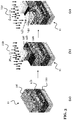
FIG. 3 andFIG. 4 show themethod 100 according to an embodiment of the invention, which builds on the embodiment shown inFIG. 1 andFIG. 2 .FIG. 3 andFIG. 4 exemplarily show a method for fabricating a vertical SGT-SRAM device 10. -
FIG. 3(a) shows that again first thesubstrate 11 is provided, e.g. grown. Thesubstrate 11 here includes three substrate layers, a p-type silicon substrate 11a, a p-type silicon layer 11b provided on the p-type silicon substrate 11a, and an n-type silicon layer 11c provide don the p-type silicon layer 11b. Conductivity types of these doped layers could also be reversed. -
FIG. 3(b) shows that then thefirst mask structure 12 is formed on thesubstrate 11. Here, thefirst mask structure 12 comprises afirst pad oxide 12a, which is provided on the entire surface of thesubstrate 11, apad nitride 12b provided on thefirst pad oxide 12a only above thesecond surface region 15b of thesubstrate 11, and a firsthard mask oxide 12c provided on thepad nitride 12b. Further,FIG. 3(b) shows that ion implantation of e.g. phosphor (as the n-type dopants 13a) maybe performed to form the n-type well 13 in thesurface region 13b of the n-type silicon layer 11c of thesubstrate 11. - Afterwards, the
first mask structure 12 is removed (here not shown). Thereby, the SCROD method may be used to remove the firsthard mask oxide 12c and thepad oxide 12a, and additionally plasma etching may be used to remove thepad nitride 12b. -
FIG. 3(c) shows that then thesecond mask structure 14 is formed. Here, thesecond mask structure 14 comprises asecond pad oxide 14a provided on the entire surface of thesubstrate 11, and a second hard mask oxide 114b provided on thesecond pad oxide 14a only above thefirst surface region 13b. Further, ion implantation of e.g. boron (as the p-type dopants 15a) may be performed to form the p-type well 15 in thesecond surface region 15b of the n-type silicon layer 11c of thesubstrate 11. - Afterwards, the
second mask structure 12a is removed. Thereby, the SCROD method may be used to remove the secondhard mask oxide 14b and thesecond pad oxide 14a (here not shown). -
FIG. 4(a) shows that after the removal of thesecond mask structure 12a, the substrate surface, in particular the surfaces of the n-type well 13 (thefirst surface region 13b) and the p-type well 15 (thesecond surface region 15b) are exposed. Here, thewells -
FIG. 4(b) shows that thereafter the plurality ofsemiconductor channel structures 16 may be formed on the substrate surface, i.e. on the n-type well 13 and p-type well 15 respectively. Thechannel structures 16 are formed on both the n-type well 13 and the p-type well 15, i.e., they are formed across the n/p boundary. Multiple such n/p boundaries may exist. Thechannel structures 16 may be grown simultaneously by epitaxy, or an epitaxy layer may be grown and then structured into thechannel structures 16. Here, thechannel structures 16 are shown to be vertical nanowires or nanopillars. Exemplarily, each of thesenanowires 16 includes asemiconductor pillar 16a (e.g. a silicon pillar), anoxide layer 16b and anitride layer 16c. - The structure shown in
FIG. 4(b) may be further processed to form the final SGT-SRAM device (here not shown). For instance, the further processing steps may include surrounding each of thevertical channel structures 16 by at least one gate structure. Furthermore, the further processing steps may include structuring a bottom connection to thevertical channel structures 16, in order to make the n-type well 13 and the p-type well 15 function as source and drain contacts for thechannel structures 16, respectively. Thus, themethod 100 may further fabricate vertical GAA transistors. - In summary, the advantages of the embodiments of the invention include that they can be fabricated at low temperatures. Further, that the surfaces of the n-type well(s) 13 and p-type well(s) are optimized for further epitaxial growth. Application scenarios of the embodiments of the invention include SRAM devices, in particular, using vertical GAA transistor architectures.
Claims (14)
- A method (100) for processing a Complementary Metal-Oxide-Silicon, CMOS, device, (10) the method (100) comprising:growing a semiconductor substrate (11);forming a first mask structure (12) on the substrate (11);inserting n-type dopants (13a) into a first surface region (13b) of the substrate (11) to form an n-type well (13), wherein the first mask structure (12) prevents insertion of n-type dopants (13a) into a second surface region (15b) of the substrate (11);removing the first mask structure (12);thereafter forming a second mask structure (14) on the substrate (11);inserting p-type dopants (15a) into the second surface region (15b) of the substrate (11) to form a p-type well (15), wherein the second mask structure (14) prevents insertion of p-type dopants into the first surface region (13b) of the substrate (11);removing the second mask structure (14); andgrowing one or more vertical semiconductor channel structures (16) simultaneously on the n-type well (13) and the p-type well (15).
- The method (100) according to claim 1, wherein:
removing the first mask structure (12) and/or the second mask structure (14) comprises performing a Spin Cleaning with Repeated Ozonized water and Diluted HF, SCROD, method. - The method (100) according to claim 1 or 2, wherein:the n-well (13) and the p-well (15) are formed adjacently; anda surface step between the surface of the n-well (13) and the adjacent surface of the p-well (15) is in a range of 1-3 nm.
- The method (100) according to one of the claims 1 to 3, wherein the first mask structure (12) comprises:a first pad oxide (12a) provided on the substrate (11);a pad nitride (12b) provided on the first pad oxide (12a) above the second surface region (15b) of the substrate (11); anda first hard mask oxide (12c) provided on the pad nitride (12b).
- The method (100) according to one of the claims 1 to 4, wherein the second mask structure (14) comprises:a second pad oxide (14a) provided on the substrate (11); anda second hard mask oxide (14b) provided on the second pad oxide (14a) above the first surface region (13b) of the substrate (11).
- The method (100) according to the claims 3, 4 and 5, wherein:
the first pad oxide (12a) and the first hard mask oxide (12c), and/or the second pad oxide (14a) and the second hard mask oxide (14b), are removed by performing the SCROD method. - The method (100) according to the claims 4 and 5, or according to claim 6, wherein:
a thickness of the first pad oxide (12a) is smaller than a thickness of the second pad oxide (14a). - The method (100) according to one of the claims 1 to 7, wherein:
the n-type dopants (13a) and/or the p-type dopants (15a) are inserted into the substrate (11) by ion implantation. - The method (100) according to claims 7 and 8, wherein:the n-type dopants (13a) are ion implanted into the first surface region (13b) of the substrate (11) through the first pad oxide (12a);the p-type dopants (15a) are ion implanted into the second surface region (15b) of the substrate (11) through the second pad oxide (14a); andthe ion implantation doses and/or energies for the n-type dopants (13) and the p-type dopants (15) are, respectively, selected based on the thickness of the first pad oxide (12a) and the thickness of the second pad oxide (14a), to obtain an equal depth profile of the n-dopants (13a) in the n-well (13) and the p-dopants (15a) in the p-well (15).
- The method (100) according to one of the claims 1 to 9, wherein:
the one or more vertical semiconductor channel structures (16) comprise one or more vertical semiconductor nanowires or nanowire pillars. - The method (100) according to one of the claims 1 to 10, wherein:
the semiconductor substrate (11) is a silicon substrate or a silicon-based substrate. - The method (100) according to one of the claims 1 to 11, wherein:
each of the one or more vertical semiconductor channel structures (16) comprises a channel made of silicon, silicon germanium, germanium, or a III-V semiconductor material. - The method (100) according to one of the claims 1 to 12, wherein:the CMOS device (10) is vertical CMOS device and/or a 3D Static Random Access Memory, SRAM device; and/orthe CMOS device is a vertical CMOS device and/or a Surrounding Gate Transistor SRAM, SGT-SRAM, device, wherein each of the one or more vertical semiconductor channel structures (16) is surrounded by at least one gate structure.
- A CMOS device (10) fabricated using the method (100) according to any one of the claims 1 to 13.
Priority Applications (1)
| Application Number | Priority Date | Filing Date | Title |
|---|---|---|---|
| EP20164201.4A EP3882962A1 (en) | 2020-03-19 | 2020-03-19 | Method for fabricating a cmos device |
Applications Claiming Priority (1)
| Application Number | Priority Date | Filing Date | Title |
|---|---|---|---|
| EP20164201.4A EP3882962A1 (en) | 2020-03-19 | 2020-03-19 | Method for fabricating a cmos device |
Publications (1)
| Publication Number | Publication Date |
|---|---|
| EP3882962A1 true EP3882962A1 (en) | 2021-09-22 |
Family
ID=69903029
Family Applications (1)
| Application Number | Title | Priority Date | Filing Date |
|---|---|---|---|
| EP20164201.4A Withdrawn EP3882962A1 (en) | 2020-03-19 | 2020-03-19 | Method for fabricating a cmos device |
Country Status (1)
| Country | Link |
|---|---|
| EP (1) | EP3882962A1 (en) |
Citations (2)
| Publication number | Priority date | Publication date | Assignee | Title |
|---|---|---|---|---|
| US20180138091A1 (en) * | 2015-12-22 | 2018-05-17 | International Business Machines Corporation | Vertical fets with variable bottom spacer recess |
| EP3435413A1 (en) * | 2017-07-28 | 2019-01-30 | IMEC vzw | A semiconductor device and a method for forming a semiconductor device |
-
2020
- 2020-03-19 EP EP20164201.4A patent/EP3882962A1/en not_active Withdrawn
Patent Citations (2)
| Publication number | Priority date | Publication date | Assignee | Title |
|---|---|---|---|---|
| US20180138091A1 (en) * | 2015-12-22 | 2018-05-17 | International Business Machines Corporation | Vertical fets with variable bottom spacer recess |
| EP3435413A1 (en) * | 2017-07-28 | 2019-01-30 | IMEC vzw | A semiconductor device and a method for forming a semiconductor device |
Non-Patent Citations (2)
| Title |
|---|
| HATTORI T: "ENVIRONMENTALLY FRIENDLY SINGLE-WAFER SPIN CLEANING", SOLID STATE TECHNOLOGY, PENNWELL CORPORATION, TULSA, OK, US, vol. 42, no. 11, November 1999 (1999-11-01), XP000860702, ISSN: 0038-111X * |
| KIM M-S ET AL: "12-EUV Layer Surrounding Gate Transistor (SGT) for Vertical 6-T SRAM: 5-nm-class Technology for Ultra-Density Logic Devices", 2019 SYMPOSIUM ON VLSI TECHNOLOGY, THE JAPAN SOCIETY OF APPLIED PHYSICS, 9 June 2019 (2019-06-09), XP033578802, DOI: 10.23919/VLSIT.2019.8776532 * |
Similar Documents
| Publication | Publication Date | Title |
|---|---|---|
| US8021949B2 (en) | Method and structure for forming finFETs with multiple doping regions on a same chip | |
| CN106328538B (en) | Self-aligned SiGe FinFET | |
| US7951657B2 (en) | Method of forming a planar field effect transistor with embedded and faceted source/drain stressors on a silicon-on-insulator (S0I) wafer, a planar field effect transistor structure and a design structure for the planar field effect transistor | |
| TWI540731B (en) | Transistor element and method of forming same | |
| KR101180978B1 (en) | Transistor device having an increased threshold stability without drive current degradation | |
| US9349862B2 (en) | Method of fabricating semiconductor devices | |
| KR101811109B1 (en) | Deeply depleted mos transistors having a screening layer and methods thereof | |
| JP5735767B2 (en) | Integrated circuit structure and manufacturing method thereof | |
| US9245955B2 (en) | Embedded shape SiGe for strained channel transistors | |
| US10170475B2 (en) | Silicon-on-nothing transistor semiconductor structure with channel epitaxial silicon region | |
| US9620507B2 (en) | Silicon-on-nothing transistor semiconductor structure with channel epitaxial silicon-germanium region | |
| KR101967531B1 (en) | Improved pmos finfet | |
| CN102290374A (en) | Method for manufacturing integrated circuit device | |
| JP2010538496A (en) | Integration of double gate oxide devices | |
| US10325913B2 (en) | Method, apparatus, and system having super steep retrograde well with engineered dopant profiles | |
| WO2012062791A1 (en) | Creating anisotrpically diffused junctions in field effect transistor devices | |
| US9761679B2 (en) | Performance optimized gate structures having memory device and logic device, the memory device with silicided source/drain regions that are raised with respect to silicided source/drain regions of the logic device | |
| US20120139033A1 (en) | Semiconductor device and method of manufacturing the same | |
| US20190027400A1 (en) | Technique for patterning active regions of transistor elements in a late manufacturing stage | |
| US9041119B2 (en) | Forming CMOS with close proximity stressors | |
| US20120315734A1 (en) | Method for fabricating semiconductor device | |
| KR20080074342A (en) | Transistor Formation Method of Semiconductor Device | |
| CN103871967A (en) | Forming method of CMOS (complementary metal oxide semiconductor) transistor | |
| KR20070002575A (en) | Manufacturing method of semiconductor device | |
| CN104465382A (en) | Method for forming source drain of MOS transistor |
Legal Events
| Date | Code | Title | Description |
|---|---|---|---|
| PUAI | Public reference made under article 153(3) epc to a published international application that has entered the european phase |
Free format text: ORIGINAL CODE: 0009012 |
|
| STAA | Information on the status of an ep patent application or granted ep patent |
Free format text: STATUS: THE APPLICATION HAS BEEN PUBLISHED |
|
| AK | Designated contracting states |
Kind code of ref document: A1 Designated state(s): AL AT BE BG CH CY CZ DE DK EE ES FI FR GB GR HR HU IE IS IT LI LT LU LV MC MK MT NL NO PL PT RO RS SE SI SK SM TR |
|
| STAA | Information on the status of an ep patent application or granted ep patent |
Free format text: STATUS: THE APPLICATION IS DEEMED TO BE WITHDRAWN |
|
| 18D | Application deemed to be withdrawn |
Effective date: 20220323 |