EP3882959A1 - Protective film forming agent for plasma dicing and method for manufacturing semiconductor chip - Google Patents
Protective film forming agent for plasma dicing and method for manufacturing semiconductor chip Download PDFInfo
- Publication number
- EP3882959A1 EP3882959A1 EP19883381.6A EP19883381A EP3882959A1 EP 3882959 A1 EP3882959 A1 EP 3882959A1 EP 19883381 A EP19883381 A EP 19883381A EP 3882959 A1 EP3882959 A1 EP 3882959A1
- Authority
- EP
- European Patent Office
- Prior art keywords
- protective film
- forming agent
- water
- film forming
- mass
- Prior art date
- Legal status (The legal status is an assumption and is not a legal conclusion. Google has not performed a legal analysis and makes no representation as to the accuracy of the status listed.)
- Granted
Links
Images


Classifications
-
- H—ELECTRICITY
- H10—SEMICONDUCTOR DEVICES; ELECTRIC SOLID-STATE DEVICES NOT OTHERWISE PROVIDED FOR
- H10P—GENERIC PROCESSES OR APPARATUS FOR THE MANUFACTURE OR TREATMENT OF DEVICES COVERED BY CLASS H10
- H10P50/00—Etching of wafers, substrates or parts of devices
- H10P50/69—Etching of wafers, substrates or parts of devices using masks for semiconductor materials
- H10P50/691—Etching of wafers, substrates or parts of devices using masks for semiconductor materials for Group V materials or Group III-V materials
- H10P50/692—Etching of wafers, substrates or parts of devices using masks for semiconductor materials for Group V materials or Group III-V materials characterised by their composition, e.g. multilayer masks or materials
-
- H—ELECTRICITY
- H10—SEMICONDUCTOR DEVICES; ELECTRIC SOLID-STATE DEVICES NOT OTHERWISE PROVIDED FOR
- H10P—GENERIC PROCESSES OR APPARATUS FOR THE MANUFACTURE OR TREATMENT OF DEVICES COVERED BY CLASS H10
- H10P54/00—Cutting or separating of wafers, substrates or parts of devices
-
- B—PERFORMING OPERATIONS; TRANSPORTING
- B23—MACHINE TOOLS; METAL-WORKING NOT OTHERWISE PROVIDED FOR
- B23K—SOLDERING OR UNSOLDERING; WELDING; CLADDING OR PLATING BY SOLDERING OR WELDING; CUTTING BY APPLYING HEAT LOCALLY, e.g. FLAME CUTTING; WORKING BY LASER BEAM
- B23K26/00—Working by laser beam, e.g. welding, cutting or boring
- B23K26/36—Removing material
- B23K26/362—Laser etching
- B23K26/364—Laser etching for making a groove or trench, e.g. for scribing a break initiation groove
-
- C—CHEMISTRY; METALLURGY
- C09—DYES; PAINTS; POLISHES; NATURAL RESINS; ADHESIVES; COMPOSITIONS NOT OTHERWISE PROVIDED FOR; APPLICATIONS OF MATERIALS NOT OTHERWISE PROVIDED FOR
- C09D—COATING COMPOSITIONS, e.g. PAINTS, VARNISHES OR LACQUERS; FILLING PASTES; CHEMICAL PAINT OR INK REMOVERS; INKS; CORRECTING FLUIDS; WOODSTAINS; PASTES OR SOLIDS FOR COLOURING OR PRINTING; USE OF MATERIALS THEREFOR
- C09D101/00—Coating compositions based on cellulose, modified cellulose, or cellulose derivatives
- C09D101/08—Cellulose derivatives
- C09D101/26—Cellulose ethers
- C09D101/28—Alkyl ethers
- C09D101/284—Alkyl ethers with hydroxylated hydrocarbon radicals
-
- C—CHEMISTRY; METALLURGY
- C09—DYES; PAINTS; POLISHES; NATURAL RESINS; ADHESIVES; COMPOSITIONS NOT OTHERWISE PROVIDED FOR; APPLICATIONS OF MATERIALS NOT OTHERWISE PROVIDED FOR
- C09D—COATING COMPOSITIONS, e.g. PAINTS, VARNISHES OR LACQUERS; FILLING PASTES; CHEMICAL PAINT OR INK REMOVERS; INKS; CORRECTING FLUIDS; WOODSTAINS; PASTES OR SOLIDS FOR COLOURING OR PRINTING; USE OF MATERIALS THEREFOR
- C09D139/00—Coating compositions based on homopolymers or copolymers of compounds having one or more unsaturated aliphatic radicals, each having only one carbon-to-carbon double bond, and at least one being terminated by a single or double bond to nitrogen or by a heterocyclic ring containing nitrogen; Coating compositions based on derivatives of such polymers
- C09D139/04—Homopolymers or copolymers of monomers containing heterocyclic rings having nitrogen as ring member
-
- C—CHEMISTRY; METALLURGY
- C09—DYES; PAINTS; POLISHES; NATURAL RESINS; ADHESIVES; COMPOSITIONS NOT OTHERWISE PROVIDED FOR; APPLICATIONS OF MATERIALS NOT OTHERWISE PROVIDED FOR
- C09D—COATING COMPOSITIONS, e.g. PAINTS, VARNISHES OR LACQUERS; FILLING PASTES; CHEMICAL PAINT OR INK REMOVERS; INKS; CORRECTING FLUIDS; WOODSTAINS; PASTES OR SOLIDS FOR COLOURING OR PRINTING; USE OF MATERIALS THEREFOR
- C09D177/00—Coating compositions based on polyamides obtained by reactions forming a carboxylic amide link in the main chain; Coating compositions based on derivatives of such polymers
- C09D177/06—Polyamides derived from polyamines and polycarboxylic acids
-
- C—CHEMISTRY; METALLURGY
- C09—DYES; PAINTS; POLISHES; NATURAL RESINS; ADHESIVES; COMPOSITIONS NOT OTHERWISE PROVIDED FOR; APPLICATIONS OF MATERIALS NOT OTHERWISE PROVIDED FOR
- C09D—COATING COMPOSITIONS, e.g. PAINTS, VARNISHES OR LACQUERS; FILLING PASTES; CHEMICAL PAINT OR INK REMOVERS; INKS; CORRECTING FLUIDS; WOODSTAINS; PASTES OR SOLIDS FOR COLOURING OR PRINTING; USE OF MATERIALS THEREFOR
- C09D7/00—Features of coating compositions, not provided for in group C09D5/00; Processes for incorporating ingredients in coating compositions
- C09D7/40—Additives
- C09D7/41—Organic pigments; Organic dyes
-
- H—ELECTRICITY
- H10—SEMICONDUCTOR DEVICES; ELECTRIC SOLID-STATE DEVICES NOT OTHERWISE PROVIDED FOR
- H10P—GENERIC PROCESSES OR APPARATUS FOR THE MANUFACTURE OR TREATMENT OF DEVICES COVERED BY CLASS H10
- H10P50/00—Etching of wafers, substrates or parts of devices
- H10P50/20—Dry etching; Plasma etching; Reactive-ion etching
- H10P50/24—Dry etching; Plasma etching; Reactive-ion etching of semiconductor materials
- H10P50/242—Dry etching; Plasma etching; Reactive-ion etching of semiconductor materials of Group IV materials
-
- H—ELECTRICITY
- H10—SEMICONDUCTOR DEVICES; ELECTRIC SOLID-STATE DEVICES NOT OTHERWISE PROVIDED FOR
- H10W—GENERIC PACKAGES, INTERCONNECTIONS, CONNECTORS OR OTHER CONSTRUCTIONAL DETAILS OF DEVICES COVERED BY CLASS H10
- H10W74/00—Encapsulations, e.g. protective coatings
- H10W74/01—Manufacture or treatment
Definitions
- the present invention relates to a protective film forming agent for plasma dicing, and a method for producing semiconductor chips using this protective film forming agent for plasma dicing.
- a wafer formed in a semiconductor device manufacturing process has a laminated body in which an insulating film and functional film are laminated on a surface of a semiconductor substrate such as silicon, and is demarcated by a lattice of scheduled division lines called streets, and thus the respective regions demarcated by the streets define semiconductor chips such as IC and LSI.
- an optical device wafer has a laminated body in which a gallium nitride-based compound semiconductor or the like is laminated, and is demarcated into a plurality of regions by the streets. By cutting along these streets, the optical device wafer is divided into optical devices such as light emitting diodes or laser diodes. These optical devices are widely applied to electronic equipment.
- Patent Document 1 Japanese Unexamined Patent Application (Translation of PCT Application), Publication No. 2014-523112
- Patent Document 1 in the case of forming a protective film having resistance to plasma dicing, there have been cases where an opening (processed groove) of the desired shape is hardly formed by irradiation of a laser beam at the desired position of the protective film.
- the present invention has been made taking account of the above problem, and has an object of providing a protective film forming agent for plasma dicing which can favorably form an opening (processed groove) of a desired shape by irradiation of a laser beam, at a desired position of the protective film, upon producing semiconductor chips by cutting a semiconductor substrate by plasma dicing, and a method for producing a semiconductor chip using this protective film forming agent for plasma dicing.
- the present inventors found that the above-mentioned problem could be solved by using a water-soluble resin (A) exhibiting a weight loss rate of at least 80 weight% in the case of raising temperature to 500°C in thermogravimetry, in a protective film forming agent for plasma dicing containing the water-soluble resin (A), a light absorber (B) and solvent (S), thereby arriving at completing the present invention. More specifically, the present invention provides the following.
- a first aspect of the present invention is a protective film forming agent for plasma dicing, including a water-soluble resin (A), a light absorber (B) and a solvent (S), in which a weight loss rate in a case of raising temperature to 500°C in thermogravimetry of the water-soluble resin (A) is at least 80 weight%.
- a second aspect of the present invention is a method for producing semiconductor chips which cuts a semiconductor wafer by plasma dicing, the method including the steps of:
- a protective film forming agent for plasma dicing which can favorably form an opening (processed groove) of a desired shape by irradiation of a laser beam, at a desired position of the protective film, upon producing semiconductor chips by cutting a semiconductor substrate by plasma dicing, and a method for producing a semiconductor chip using this protective film forming agent for plasma dicing.
- a protective film forming agent for plasma dicing contains a water-soluble resin (A), a light absorber (B) and a solvent (S).
- a protective film forming agent for plasma dicing is also noted as “protective film forming agent”.
- the protective film forming agent for plasma dicing is used in the formation of a protective film in the manufacturing method of semiconductor chips including: irradiating a laser beam on a protective film formed on a semiconductor wafer, the surface of the semiconductor wafer being exposed, and then forming a processed groove of a pattern according to the shape of the semiconductor chip; and irradiating plasma on the semiconductor wafer including the above-mentioned protective film and the above-mentioned processed groove to cut the position of the processed groove on the semiconductor wafer.
- the film thickness of the protective film is preferably at least 1 ⁇ m to no more than 100 ⁇ m, more preferably at least 10 ⁇ m to no more than 100 ⁇ m, and even more preferably at least 30 ⁇ m to no more than 100 ⁇ m.
- the water-soluble resin (A) exhibits a weight loss rate of at least 80 weight% in the case of heating to 500°C in thermogravimetry. In other words, the majority of the water-soluble resin (A) decomposes and is lost when heated to on the order of 500°C.
- the water-soluble resin (A) is a base material of the protective film formed using the protective film forming agent.
- the type of water-soluble resin is not particular limited so long as being a resin which can form a film by dissolving in a solvent such as water, then coating and drying, and exhibiting a weight loss rate of at least 80 weight% in the case of heating to 500°C.
- Water-soluble refers to at least 0.5 g of the solute (water-soluble resin) dissolving in 100 g of water at 25°C.
- the water-soluble resin (A) is a resin which exhibits a weight loss rate of at least 80 weight% in the case of heating up to 500°C in thermogravimetry.
- the weight loss rate in the case of heating up to 500°C is more preferably at least 90 weight%, and even more preferably at least 95 weight%.
- a protective film forming agent containing a water-soluble resin (A) for which the weight loss rate when heating up to 500°C is within the above-mentioned range since decomposition of the water-soluble resin (A) favorably progresses from the energy of the laser beam in the protective film, a processed groove that is favorably opened in the protective film tends to form by the irradiation of a laser beam.
- the water-soluble resin (A), the weight loss rate when heating up to 350°C in thermogravimetry is preferably at least 10 weight%, and more preferably at least 15 weight%.
- the water-soluble resin (A) tends to favorably decompose, and even in the case of irradiating a low-output laser, a processed groove favorably opening in the protective film tends to be formed.
- thermogravimetry for obtaining the weight loss rate can be performed in accordance with a common thermogravimetry method.
- the method for adjusting the weight loss rate of the water-soluble resin (A) is not particularly limited. Generally, so long as being the same type of resin, the weight loss rate of the water-soluble resin (A) will be higher with a smaller average molecular weight.
- the weight average molecular weight of the water-soluble resin (A) is preferably at least 15,000 to no more than 300,000, and more preferably at least 20,000 to no more than 200,000.
- water-soluble resin (A) As a specific example for the type of water-soluble resin (A), it is possible to exemplify a vinyl resin, cellulose resin, polyethylene oxide, polyglycerin, water-soluble nylon, etc.
- the vinyl resin is not particularly limited, so long as being a homopolymer or copolymer of monomers having a vinyl group, and being a water-soluble resin.
- the cellulose resin is not particularly limited so long as being a water-soluble cellulose derivative.
- methyl cellulose, ethyl cellulose, hydroxypropyl cellulose, etc. can be exemplified. These can be used independently as one type, or can be used by combining two or more types.
- a vinyl resin and cellulose resin are preferable, and polyvinyl pyrrolidone and hydroxypropyl cellulose are more preferable.
- the protective film formed on the semiconductor wafer surface normally is removed by water washing after the plasma dicing process. For this reason, a water-soluble resin having low affinity with the semiconductor wafer surface is preferable from the point of water washability of the protective film.
- a resin having only an ether linkage, hydroxyl group, or amide bond as polar groups for example, polyvinyl alcohol, polyethylene glycol, polyvinyl pyrrolidine, and hydroxypropyl cellulose, are preferable.
- the ratio of the mass of water-soluble resin (A) relative to the total amount of the mass of water-soluble resin (A) and mass of light absorber (B) in the protective film forming agent is preferably at least 60% by mass to no more than 99% by mass, and more preferably at least 80% by mass to no more than 95% by mass.
- the protective film forming agent contains a light absorber (B) with the purpose of efficiently absorbing the energy of the laser beam in the protective film, and promoting the thermal decomposition of the protective film.
- a light absorber (B) it is not particularly limited so long as being a material which is blended into the protective film to which the laser beam is irradiated conventionally in the dicing process of semiconductor wafers, and having absorbency for laser beams.
- the light absorber (B) it is possible to use a water-soluble dye, water soluble colorant, water-soluble ultraviolet absorber, etc. These are all water soluble, and are advantageous upon uniformly present in the protective film. In addition, these exhibit high affinity to the semiconductor wafer surface. For this reason, when using a protective film forming agent including these light absorbers (B), a protective film having high adhesion to the semiconductor wafer surface tends to be formed.
- the storage stability of the protective film forming agent is high, and since flaws such as phase separation of the protective film forming agent and precipitation of the light absorber (B) will not be induced during storage of the protective film forming agent, it is advantageous also in the point of tending to maintain favorable coatability of the protective film forming agent for a long period.
- a water insoluble light absorber such as a pigment can also be used.
- a water-insoluble light absorber although fatal obstacles to use of the protective film forming agent will not arise, variation in the laser absorptivity of the protective film may arise, it may be difficult to obtain a protective film forming agent that excels in storage stability and coatability, and it may be difficult to form a protective film of uniform thickness.
- a water-soluble dye is selected from among azo dyes such monoazo dyes, polyazo dyes, metal complex azo dyes, pyrazolone azo dyes, stilbene azo dyes and thiazole azo dyes; anthraquinone dyes such as anthraquinone derivatives and anthrone derivatives; indigoid dyes such as indigoid derivatives and thioindigoide derivatives; phthalocyanine dyes; carbonium dyes such as diphenylmethane dyes, triphenylmethane dyes, xanthene dyes and acridine dyes; quinone imine dyes such as azine dyes, oxazine dyes and thiazine dyes; methine dyes such as cyanine dyes and azomethine dyes; quinoline dyes; nitroso dyes; benzoquinone and naphthoquinone dyes;
- colorants for food additives such as Food Red No. 2, Food Red No. 40, Food Red No. 102, Food Red No. 104, Food Red No. 105, Food Red No. 106, Food Yellow NY, Food Yellow No. 4 tartrazine, Food Yellow No. 5, Food Yellow No. 5 Sunset Yellow FCF, Food Orange AM, Food Vermillion No. 1, Food Vermillion No. 4, Food Vermillion No. 101, Food Blue No. 1, Food Blue No. 2, Food Green No. 3, Food Melon Color B, and Food Egg Color No. 3 are preferred from the viewpoint of environmental load, etc.
- the water-soluble ultraviolet absorber for example, it is possible to exemplify organic acids such as 4,4'-dicarboxybenzophenone, benzophenone-4-carboxylic acid, 2-carboxyanthraquinone, 1,2-naphthalenedicarboxylic acid, 1,8-naphthalenedicarboxylic acid, 2,3-naphthalenedicarboxylic acid, 2,6-naphthalenedicarboxylic acid, and 2,7-naphthalenedicarboxylic acid, 4-aminocinnamic acid, 3-aminocinnamic acid, 2-aminocinnamic acid, sinapic acid (3,5-dimethoxy-4-hydroxycinnamic acid), ferulic acid, caffeine acid, biphenyl-4-sulfonic acid, 2,6-anthraquinone disulfonic acid, 2,7-anthraquinone disulfonic acid, curcumin and tetrahydroxybenzophenone; sodium salts, potassium salt, potassium
- 4-aminocinnamic acid, 3-aminocinnamic acid, 2-aminocinnamic acid and ferulic acid are preferable, 4-aminocinnamic acid and ferulic acid are more preferable, and 4-aminocinnamic acid is particularly preferable.
- the ratio of the mass of light absorber (B) relative to the total amount of the mass of water-soluble resin (A) and mass of light absorber (B) in the protective film forming agent is preferably at least 1% by mass to no more than 40% by mass, and more preferably at least 5% by mass to no more than 20% by mass.
- the protective film forming agent may contain other compounding agents unless inhibiting the object of the present invention, in addition to the water-soluble resin (A) and light absorber (B).
- the other compounding agent for example, it is possible to use preservatives, surfactants, etc.
- preservative it is possible to use benzoic acid, butylparaben, ethylparaben, methylparaben, propylparaben, sodium benzoate, sodium propionate, benzalkonium chloride, benzyl alcohol, cetylpyridinium chloride, chlorobutanol, phenol, phenylethyl alcohol, 2-phenoxyethanol, phenylmercuric nitrate, thimerosal, metacresol, lauryldimethylamine oxide, and combinations of these.
- a preservative is preferable not only from the point of preservation of the protective film forming agent, but also the point of a load reduction in the processing of waste liquid after semiconductor wafer washing.
- a large amount of washing water is generally used for washing of semiconductor wafers.
- proliferation of bacteria in the waste liquid is of concern due to the water-soluble resin (A) contained in the protective film forming agent.
- the surfactant for example, is used in order to raise the defoaming property during protective film forming agent production, stability of the protective film forming agent, coatability of the protective film forming agent, etc.
- a surfactant in the point of the defoaming property during protective film forming agent production.
- a protective film is generally formed by spin coating the protective film forming agent.
- surface irregularities caused by bubbles may occur upon forming the protective film.
- an anti-foaming agent such as a surfactant.
- a water-soluble surfactant can be used preferably.
- any of nonionic surfactant, cationic surfactant, anionic surfactant and amphoteric surfactant can be used.
- the surfactant may be silicone based.
- a nonionic surfactant is preferable from the point of washability.
- the protective film forming agent usually contains a solvent (S) for dissolving the water-soluble resin (A) and light absorber (B).
- a solvent (S) for dissolving the water-soluble resin (A) and light absorber (B).
- water is normally used.
- the protective film forming agent may contain an organic solvent together with the water as the solvent (S), within a range not inhibiting the object of the present invention.
- an organic solvent which can be contained in the protective film forming agent it is possible to exemplify methyl alcohol, ethyl alcohol, alkylene glycol, alkylene glycol monoalkyl ether, alkylene glycol monoalkyl ether acetate and the like.
- alkylene glycol it is possible to exemplify ethylene glycol, propylene glycol and the like.
- alkylene glycol monoalkyl ether it is possible to exemplify ethylene glycol monomethyl ether, ethylene glycol monoethyl ether, propylene glycol monomethyl ether, propylene glycol monoethyl ether and the like.
- alkylene glycol monoalkyl ether acetate it is possible to exemplify ethylene glycol monomethyl ether acetate, ethylene glycol monoethyl ether acetate, propylene glycol monomethyl ether acetate, propylene glycol monoethyl ether acetate and the like.
- the protective film forming agent may contain a combination of two or more types of organic solvent.
- the concentration of the organic solvent in the solvent (S) may be no more than 50 mass%, may be no more than 30 mass%, or may be no more than 20 mass%, for example.
- the solid content concentration of the protective film forming agent is not particularly limited in a range not inhibiting the object of the present invention.
- the solid content concentration for example, is preferably at least 5% by mass to no more than 60% by mass, and more preferably at least 10% by mass to no more than 50% by mass.
- a method for producing a semiconductor chip is a method including cutting a semiconductor wafer by plasma dicing. More specifically, the method for producing a semiconductor chip is a method including:
- a protective film is formed by coating the aforementioned protective film forming agent on a semiconductor wafer.
- the shape of the processed surface of the semiconductor wafer is not particularly limited so long as being able to conduct the desired processing on the semiconductor wafer.
- the processed surface of the semiconductor wafer has several surface irregularities. Then, a recessed part in a region corresponding to a street is formed. In the processed surface of the semiconductor wafer, a plurality of regions corresponding to semiconductor chips is demarcated by the streets.
- the film thickness of the protective film is preferably at least 1 ⁇ m to no more than 100 ⁇ m, and more preferably at least 10 ⁇ m to no more than 100 ⁇ m. It is more preferably at least 30 ⁇ m to no more than 100 ⁇ m.
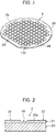
- FIG. 1 shows a perspective view of a semiconductor wafer which is a processing target.
- FIG. 2 shows an enlarged cross-sectional view of main parts of the semiconductor wafer shown in FIG. 1 .
- a laminated body 21 in which a functional films forming an insulating film and circuit are laminated is provided on a surface 20a of a semiconductor substrate 20 such as silicon.
- a plurality of semiconductor chips 22 such as IC and LSI is formed in a matrix state.
- the shape and size of the semiconductor chips 22 are not particularly limited, and can be appropriately set according to the design of the semiconductor chip 22.
- the insulating film used as the laminated body 21 consists of a SiO 2 film, an inorganic film such as SiOF, BSC (SiOB) or the like, or a low-dielectric constant insulating film (Low-k film) consisting of an organic film, which is a polymer film such as of polyimide type or parylene type.
- the surface of the above-mentioned laminated body 21 corresponds to the surface 2a which is the processed surface.
- the protective film is formed using the aforementioned protective film forming agent on the above-mentioned surface 2a.
- the protective film is formed by coating the protective film forming agent on the surface 2a of the semiconductor wafer 2 by spin coating.
- the coating method of the protective film forming agent is not particular limited so long as being able to form a protective film of the desired film thickness.
- the protective film forming agent of liquid form coating the surface 2a is dried.
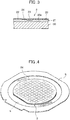
- a protective film 24 is thereby formed on the surface 2a of the semiconductor wafer 2 as shown in FIG. 3 .
- protective tape 6 put onto an annular frame 5 is pasted to the back surface of the semiconductor wafer 2, as shown in FIG. 4 .
- a laser beam is irradiated onto a predetermined position of at least one layer including the protective film 24 on the semiconductor wafer 2, the surface 20a of the semiconductor substrate 20 being exposed, whereby the processed groove of a pattern according to the shape of the semiconductor chip 22 is formed.
- a laser beam is irradiated through the protective film 24 to the surface 2a (street 23) of the semiconductor wafer 2. Irradiation of this laser beam is carried out using a laser photoirradiation means 72 as shown in FIG. 5 .
- the laser is preferably an ultraviolet laser having a wavelength of 100 nm to 400 nm from the point of intensity.
- a YVO4 laser and YAG laser of 266 nm, 355 nm, etc. wavelength, are preferable.
- the above-mentioned laser beam irradiation in the processed groove forming step is performed at the following processing conditions, for example. It should be noted that the focus spot diameter is appropriately selected considering the width of the processed groove 25.
- the processed groove 25 is formed along the street 23 in the laminated body 21 including the street 23 of the semiconductor wafer 2, as shown in FIG. 6 .
- the semiconductor wafer 2 retained on a chuck table 71 is indexed by intervals of the street in the direction indicated by the arrow Y, and irradiation of the laser beam is carried out again.
- the semiconductor wafer 2 retained on the chuck table 71 is rotated by 90 degrees, and the irradiation of the laser beam and indexing is executed as described above along each street 23 extending at a right angle relative to the above-mentioned predetermined direction. In this way, it is possible to form the processed groove 25 along all of the streets 23 formed in the laminated body 21 on the semiconductor wafer 2.
- plasma is irradiated onto the semiconductor wafer 2 including the protective film 24 and processed groove 25.
- the position of the processed groove 25 in the semiconductor wafer 2 is cut as shown in FIG. 8 . More specifically, in the semiconductor wafer 2 coated by the protective film 24, after forming the processed groove 25 as described above, by performing plasma irradiation on the protective film 24 and surface 20a of the semiconductor substrate 20 exposed from the processed groove 25, the semiconductor wafer 2 is cut following the shape of the semiconductor chips 22, and the semiconductor wafer 2 is divided into the semiconductor chips 22.
- the plasma irradiation conditions are not particularly limited so long as being able to favorably perform cutting of the semiconductor wafer 2 at the position of the processed groove 25.
- the plasma irradiation conditions are appropriately set within a range of common conditions of plasma etching on a semiconductor substrate, considering the material of the semiconductor wafer 2, plasma type and the like.
- the gas used for generating plasma in the plasma irradiation is appropriately selected according to the material of the semiconductor wafer 2. Typically, SF 6 gas is used in the generation of the plasma.
- SF 6 gas is used in the generation of the plasma.
- cutting of the semiconductor wafer 2 may be performed. According to the BOSCH process, etching with a high-aspect ratio is possible, and even in a case of the semiconductor wafer 2 being thick, cutting of the semiconductor wafer 2 is easy.
- the protective film 24 covering the surface of the semiconductor chip 22 is removed.
- the protective film 24 is formed using the protective film forming agent containing the water-soluble resin (A); therefore, it is possible to wash away the protective film 24 using water (or hot water).
- a production method of semiconductor chips by plasma dicing of a semiconductor wafer has been explained above based on the embodiment.
- the protective film forming agent and production method of semiconductor chips according to the present invention can be applied to production methods of various semiconductor chips, so long as being a method producing semiconductor chips by dividing a semiconductor wafer by plasma dicing.
- WSR1 to WSR5 were used as the water-soluble resin.
- Table 1 notes the weight loss rate of each water-soluble resin in the case of heating to 500°C or 350°C in the thermogravimetry measured by the method described below. Thermogravimetry was performed at the following conditions, using a TG/DTA device (Differential thermal - thermogravimetric simultaneous measurement device; TG/DTA6200R manufactured by Hitachi High Tech Science Corp.).
- TG/DTA device Different thermal - thermogravimetric simultaneous measurement device; TG/DTA6200R manufactured by Hitachi High Tech Science Corp.
- LB1 and LB2 described below were used as the light absorber.
- the water-soluble resin (A) of the type described in Table 1, and the light absorber (B) of the type described in Table 1 were uniformly dissolved in the solvent (S) in the composition described in Table 1 so as to make the solid component concentration described in Table 1, thereby obtaining the protective film forming agents of each Example and each Comparative Example.
- the protective film forming agent was coated by a spin coating method on the Si substrate. After coating, the coated film was dried for 5 minutes at 70°C, whereby a protective film of 30 ⁇ m film thickness was formed. Next, laser processing was performed at the following conditions on the protective film to remove the protective film and form a processed groove.
- the formed processed groove was observed by microscope, and evaluation of the processed groove formation was performed according to the following criteria.
- a linear processed groove of a desired shape could be formed at the desired position of the protective film, in the case of using the protective film forming agent of each Example prepared using the water-soluble resin having a weight loss rate when raising the temperature to 500°C in thermogravimetry of at least 80 weight%.
- a linear processed groove of a desired shape could not be formed at the desired position of the protective film, in the case of using the protective film forming agent of each Comparative Example prepared using the water-soluble resin having a weight loss rate when raising the temperature to 500°C in thermogravimetry of less than 80 weight%.
- the shape of the opening was slightly deteriorated.
Landscapes
- Chemical & Material Sciences (AREA)
- Engineering & Computer Science (AREA)
- Materials Engineering (AREA)
- Wood Science & Technology (AREA)
- Organic Chemistry (AREA)
- Life Sciences & Earth Sciences (AREA)
- Physics & Mathematics (AREA)
- Optics & Photonics (AREA)
- Chemical Kinetics & Catalysis (AREA)
- Plasma & Fusion (AREA)
- Mechanical Engineering (AREA)
- Dicing (AREA)
- Laser Beam Processing (AREA)
Abstract
Description
- The present invention relates to a protective film forming agent for plasma dicing, and a method for producing semiconductor chips using this protective film forming agent for plasma dicing.
- A wafer formed in a semiconductor device manufacturing process has a laminated body in which an insulating film and functional film are laminated on a surface of a semiconductor substrate such as silicon, and is demarcated by a lattice of scheduled division lines called streets, and thus the respective regions demarcated by the streets define semiconductor chips such as IC and LSI.
- A plurality of semiconductor chips are obtained by cutting the wafer along these streets. In addition, an optical device wafer has a laminated body in which a gallium nitride-based compound semiconductor or the like is laminated, and is demarcated into a plurality of regions by the streets. By cutting along these streets, the optical device wafer is divided into optical devices such as light emitting diodes or laser diodes. These optical devices are widely applied to electronic equipment.
- Such cutting along the streets of a wafer has been carried out in the past by a cutting device called a dicer. However, since a wafer having a laminate structure is a highly brittle material, this method has had a problem in that, upon cutting to divide the wafer into semiconductor chips or the like by a cutting blade (cutting edge), scratches or chipping occurs, causing the insulating film required as a circuit element formed on the chip surface to peel.
- In order to avoid such flaws, a method has been proposed which forms a mask containing a layer of water-soluble material on the surface of a semiconductor substrate, then irradiates a laser on the mask, and after exposing the surface of the semiconductor substrate of a part of the mask by decomposing and removing a part of the mask, then cuts the exposed semiconductor substrate from part of the mask by plasma etching to divide the semiconductor substrate into semiconductor chips (IC) (refer to Patent Document 1).
- Patent Document 1: Japanese Unexamined Patent Application (Translation of PCT Application), Publication No.
2014-523112 - With the method disclosed in Patent Document 1, in the case of forming a protective film having resistance to plasma dicing, there have been cases where an opening (processed groove) of the desired shape is hardly formed by irradiation of a laser beam at the desired position of the protective film.
- The present invention has been made taking account of the above problem, and has an object of providing a protective film forming agent for plasma dicing which can favorably form an opening (processed groove) of a desired shape by irradiation of a laser beam, at a desired position of the protective film, upon producing semiconductor chips by cutting a semiconductor substrate by plasma dicing, and a method for producing a semiconductor chip using this protective film forming agent for plasma dicing.
- The present inventors found that the above-mentioned problem could be solved by using a water-soluble resin (A) exhibiting a weight loss rate of at least 80 weight% in the case of raising temperature to 500°C in thermogravimetry, in a protective film forming agent for plasma dicing containing the water-soluble resin (A), a light absorber (B) and solvent (S), thereby arriving at completing the present invention. More specifically, the present invention provides the following.
- A first aspect of the present invention is a protective film forming agent for plasma dicing, including a water-soluble resin (A), a light absorber (B) and a solvent (S), in which a weight loss rate in a case of raising temperature to 500°C in thermogravimetry of the water-soluble resin (A) is at least 80 weight%.
- A second aspect of the present invention is a method for producing semiconductor chips which cuts a semiconductor wafer by plasma dicing, the method including the steps of:
- forming a protective film by coating the protective film forming agent according to the first aspect on the semiconductor water;
- irradiating a laser beam on a predetermined position of at least layer containing the protective film on the semiconductor wafer, a surface of the semiconductor wafer being exposed, and then forming a processed groove of a pattern according to a shape of the semiconductor chip; and
- cutting a position of the processed groove in the semiconductor water by irradiating plasma on the semiconductor wafer which includes the protective film and the processed groove.
- According to the present invention, it is possible to provide a protective film forming agent for plasma dicing which can favorably form an opening (processed groove) of a desired shape by irradiation of a laser beam, at a desired position of the protective film, upon producing semiconductor chips by cutting a semiconductor substrate by plasma dicing, and a method for producing a semiconductor chip using this protective film forming agent for plasma dicing.
-
-
FIG. 1 is a perspective view showing a semiconductor wafer manufactured by a processing method of a wafer using the protective film forming agent of the present invention; -
FIG. 2 is a cross-sectional enlarged view of the semiconductor wafer shown inFIG. 1 ; -
FIG. 3 is an enlarged cross-sectional view of main parts of a semiconductor wafer on which a protective film was formed; -
FIG. 4 is a perspective view showing a state in which the semiconductor wafer on which the protective film was formed is supported by an annular frame via protective tape; -
FIG. 5 is a perspective view of main parts of a laser processing device which conducts laser irradiation; -
FIG. 6 is a cross-sectional enlarged view of a semiconductor wafer including a processed groove formed by laser beam irradiation; -
FIG. 7 is an explanatory view showing plasma irradiation on the semiconductor wafer shown inFIG. 6 ; -
FIG. 8 is a cross-sectional enlarged view showing a state of a semiconductor wafer being divided into semiconductor chips by plasma irradiation; and -
FIG. 9 is a cross-sectional enlarged view showing a state in which a protective film on a semiconductor chip was removed. - A protective film forming agent for plasma dicing contains a water-soluble resin (A), a light absorber (B) and a solvent (S). Hereinafter, the protective film forming agent for plasma dicing is also noted as "protective film forming agent".
- More specifically, the protective film forming agent for plasma dicing is used in the formation of a protective film in the manufacturing method of semiconductor chips including: irradiating a laser beam on a protective film formed on a semiconductor wafer, the surface of the semiconductor wafer being exposed, and then forming a processed groove of a pattern according to the shape of the semiconductor chip; and irradiating plasma on the semiconductor wafer including the above-mentioned protective film and the above-mentioned processed groove to cut the position of the processed groove on the semiconductor wafer.
- From the points of the removal of the protective film being easy by water washing after machining of the semiconductor wafer, and sufficient durability of the protective film relative to plasma irradiation, typically the film thickness of the protective film is preferably at least 1 µm to no more than 100 µm, more preferably at least 10 µm to no more than 100 µm, and even more preferably at least 30 µm to no more than 100 µm.
- The water-soluble resin (A) exhibits a weight loss rate of at least 80 weight% in the case of heating to 500°C in thermogravimetry. In other words, the majority of the water-soluble resin (A) decomposes and is lost when heated to on the order of 500°C.
- Hereinafter, components which are essentially and optionally contained by the protective film forming agent will be explained.
- The water-soluble resin (A) is a base material of the protective film formed using the protective film forming agent. The type of water-soluble resin is not particular limited so long as being a resin which can form a film by dissolving in a solvent such as water, then coating and drying, and exhibiting a weight loss rate of at least 80 weight% in the case of heating to 500°C. Water-soluble refers to at least 0.5 g of the solute (water-soluble resin) dissolving in 100 g of water at 25°C.
- As mentioned above, the water-soluble resin (A) is a resin which exhibits a weight loss rate of at least 80 weight% in the case of heating up to 500°C in thermogravimetry. The weight loss rate in the case of heating up to 500°C is more preferably at least 90 weight%, and even more preferably at least 95 weight%. In the case of using a protective film forming agent containing a water-soluble resin (A) for which the weight loss rate when heating up to 500°C is within the above-mentioned range, since decomposition of the water-soluble resin (A) favorably progresses from the energy of the laser beam in the protective film, a processed groove that is favorably opened in the protective film tends to form by the irradiation of a laser beam.
- The water-soluble resin (A), the weight loss rate when heating up to 350°C in thermogravimetry is preferably at least 10 weight%, and more preferably at least 15 weight%. In the case of using such a water-soluble resin (A), although the energy amount applied by the laser beam is small, the water-soluble resin (A) tends to favorably decompose, and even in the case of irradiating a low-output laser, a processed groove favorably opening in the protective film tends to be formed.
- The thermogravimetry for obtaining the weight loss rate can be performed in accordance with a common thermogravimetry method.
- The method for adjusting the weight loss rate of the water-soluble resin (A) is not particularly limited. Generally, so long as being the same type of resin, the weight loss rate of the water-soluble resin (A) will be higher with a smaller average molecular weight.
- From the viewpoint of a balance of degradability upon irradiating with a laser beam, and the film forming property, the weight average molecular weight of the water-soluble resin (A) is preferably at least 15,000 to no more than 300,000, and more preferably at least 20,000 to no more than 200,000.
- As a specific example for the type of water-soluble resin (A), it is possible to exemplify a vinyl resin, cellulose resin, polyethylene oxide, polyglycerin, water-soluble nylon, etc. The vinyl resin is not particularly limited, so long as being a homopolymer or copolymer of monomers having a vinyl group, and being a water-soluble resin. As the vinyl resin, a polyvinyl alcohol, polyvinyl acetal (including vinyl acetate copolymers), polyvinyl pyrrolidone, polyacrylamide, poly(N-alkyl acrylamide), polyallylamine, poly(N-alkyl allylamine), partially amidated polyallylamine, poly(diallylamine), allylamine-diallylamine copolymer, polyacrylic acid, polyvinyl alcohol polyacrylate block copolymer, and polyvinyl alcohol polyacrylate ester block copolymer can be exemplified. The cellulose resin is not particularly limited so long as being a water-soluble cellulose derivative. As the cellulose resin, methyl cellulose, ethyl cellulose, hydroxypropyl cellulose, etc. can be exemplified. These can be used independently as one type, or can be used by combining two or more types.
- Among the above-mentioned specific examples of the water-soluble resin (A), due to shape deterioration, etc. of the processed groove by heat sagging of the protective film hardly occurring, a vinyl resin and cellulose resin are preferable, and polyvinyl pyrrolidone and hydroxypropyl cellulose are more preferable.
- The protective film formed on the semiconductor wafer surface normally is removed by water washing after the plasma dicing process. For this reason, a water-soluble resin having low affinity with the semiconductor wafer surface is preferable from the point of water washability of the protective film. As the water-soluble resin having low affinity with the semiconductor wafer surface, a resin having only an ether linkage, hydroxyl group, or amide bond as polar groups, for example, polyvinyl alcohol, polyethylene glycol, polyvinyl pyrrolidine, and hydroxypropyl cellulose, are preferable.
- Since opening defects upon forming the processed groove by irradiating a laser beam on the protective film, shape deterioration of the processed groove due to heat sagging of the protective film, etc. hardly occur, the ratio of the mass of water-soluble resin (A) relative to the total amount of the mass of water-soluble resin (A) and mass of light absorber (B) in the protective film forming agent is preferably at least 60% by mass to no more than 99% by mass, and more preferably at least 80% by mass to no more than 95% by mass.
- The protective film forming agent contains a light absorber (B) with the purpose of efficiently absorbing the energy of the laser beam in the protective film, and promoting the thermal decomposition of the protective film. As the light absorber (B), it is not particularly limited so long as being a material which is blended into the protective film to which the laser beam is irradiated conventionally in the dicing process of semiconductor wafers, and having absorbency for laser beams.
- As the light absorber (B), it is possible to use a water-soluble dye, water soluble colorant, water-soluble ultraviolet absorber, etc. These are all water soluble, and are advantageous upon uniformly present in the protective film. In addition, these exhibit high affinity to the semiconductor wafer surface. For this reason, when using a protective film forming agent including these light absorbers (B), a protective film having high adhesion to the semiconductor wafer surface tends to be formed. In the case of using a water-soluble light absorber (B), the storage stability of the protective film forming agent is high, and since flaws such as phase separation of the protective film forming agent and precipitation of the light absorber (B) will not be induced during storage of the protective film forming agent, it is advantageous also in the point of tending to maintain favorable coatability of the protective film forming agent for a long period.
- It should be noted that a water insoluble light absorber such as a pigment can also be used. In the case of using a water-insoluble light absorber, although fatal obstacles to use of the protective film forming agent will not arise, variation in the laser absorptivity of the protective film may arise, it may be difficult to obtain a protective film forming agent that excels in storage stability and coatability, and it may be difficult to form a protective film of uniform thickness.
- As specific examples of the water-soluble dye, a water-soluble dye is selected from among azo dyes such monoazo dyes, polyazo dyes, metal complex azo dyes, pyrazolone azo dyes, stilbene azo dyes and thiazole azo dyes; anthraquinone dyes such as anthraquinone derivatives and anthrone derivatives; indigoid dyes such as indigoid derivatives and thioindigoide derivatives; phthalocyanine dyes; carbonium dyes such as diphenylmethane dyes, triphenylmethane dyes, xanthene dyes and acridine dyes; quinone imine dyes such as azine dyes, oxazine dyes and thiazine dyes; methine dyes such as cyanine dyes and azomethine dyes; quinoline dyes; nitroso dyes; benzoquinone and naphthoquinone dyes; naphthalimide dyes; perinone dyes and other dyes.
- As the water-soluble colorant, for example, colorants for food additives such as Food Red No. 2, Food Red No. 40, Food Red No. 102, Food Red No. 104, Food Red No. 105, Food Red No. 106, Food Yellow NY, Food Yellow No. 4 tartrazine, Food Yellow No. 5, Food Yellow No. 5 Sunset Yellow FCF, Food Orange AM, Food Vermillion No. 1, Food Vermillion No. 4, Food Vermillion No. 101, Food Blue No. 1, Food Blue No. 2, Food Green No. 3, Food Melon Color B, and Food Egg Color No. 3 are preferred from the viewpoint of environmental load, etc.
- As the water-soluble ultraviolet absorber, for example, it is possible to exemplify organic acids such as 4,4'-dicarboxybenzophenone, benzophenone-4-carboxylic acid, 2-carboxyanthraquinone, 1,2-naphthalenedicarboxylic acid, 1,8-naphthalenedicarboxylic acid, 2,3-naphthalenedicarboxylic acid, 2,6-naphthalenedicarboxylic acid, and 2,7-naphthalenedicarboxylic acid, 4-aminocinnamic acid, 3-aminocinnamic acid, 2-aminocinnamic acid, sinapic acid (3,5-dimethoxy-4-hydroxycinnamic acid), ferulic acid, caffeine acid, biphenyl-4-sulfonic acid, 2,6-anthraquinone disulfonic acid, 2,7-anthraquinone disulfonic acid, curcumin and tetrahydroxybenzophenone; sodium salts, potassium salt, ammonium salt, and quaternary ammonium salt of these organic acids; and EAB-F(4,4'-bis(diethylamino) benzophenone. Among these, 4-aminocinnamic acid, 3-aminocinnamic acid, 2-aminocinnamic acid and ferulic acid are preferable, 4-aminocinnamic acid and ferulic acid are more preferable, and 4-aminocinnamic acid is particularly preferable.
- Since opening defects upon forming the processed groove by irradiating a laser beam on the protective film, shape deterioration of the processed groove due to heat sagging of the protective film, etc. hardly occur, the ratio of the mass of light absorber (B) relative to the total amount of the mass of water-soluble resin (A) and mass of light absorber (B) in the protective film forming agent is preferably at least 1% by mass to no more than 40% by mass, and more preferably at least 5% by mass to no more than 20% by mass.
- The protective film forming agent may contain other compounding agents unless inhibiting the object of the present invention, in addition to the water-soluble resin (A) and light absorber (B). As the other compounding agent, for example, it is possible to use preservatives, surfactants, etc.
- As the preservative, it is possible to use benzoic acid, butylparaben, ethylparaben, methylparaben, propylparaben, sodium benzoate, sodium propionate, benzalkonium chloride, benzyl alcohol, cetylpyridinium chloride, chlorobutanol, phenol, phenylethyl alcohol, 2-phenoxyethanol, phenylmercuric nitrate, thimerosal, metacresol, lauryldimethylamine oxide, and combinations of these.
- Using a preservative is preferable not only from the point of preservation of the protective film forming agent, but also the point of a load reduction in the processing of waste liquid after semiconductor wafer washing. A large amount of washing water is generally used for washing of semiconductor wafers. However, in the process using the aforementioned protective film forming agent, proliferation of bacteria in the waste liquid is of concern due to the water-soluble resin (A) contained in the protective film forming agent. For this reason, it is desirable for the waste liquid derived from a process using the aforementioned protective film forming agent to be treated separately from the waste liquid derived from a process not using the protective film forming agent. However, in the case of containing a preservative in the protective film forming agent, since the proliferation of bacteria caused by the water-soluble resin (A) is suppressed, the waste liquid derived from the process using the protective film forming agent and the waste liquid derived from a process not using the protective film forming agent can be treated similarly. For this reason, it is possible to reduce the load of waste-water treatment processing.
- The surfactant, for example, is used in order to raise the defoaming property during protective film forming agent production, stability of the protective film forming agent, coatability of the protective film forming agent, etc. In particular, it is preferable to use a surfactant in the point of the defoaming property during protective film forming agent production.
- A protective film is generally formed by spin coating the protective film forming agent. However, surface irregularities caused by bubbles may occur upon forming the protective film. In order to suppress the occurrence of such surface irregularities, it is preferable to use an anti-foaming agent such as a surfactant.
- As the surfactant, a water-soluble surfactant can be used preferably. As the surfactant, any of nonionic surfactant, cationic surfactant, anionic surfactant and amphoteric surfactant can be used. The surfactant may be silicone based. A nonionic surfactant is preferable from the point of washability.
- The protective film forming agent usually contains a solvent (S) for dissolving the water-soluble resin (A) and light absorber (B). As the solvent (S), water is normally used. The protective film forming agent may contain an organic solvent together with the water as the solvent (S), within a range not inhibiting the object of the present invention. As examples of an organic solvent which can be contained in the protective film forming agent, it is possible to exemplify methyl alcohol, ethyl alcohol, alkylene glycol, alkylene glycol monoalkyl ether, alkylene glycol monoalkyl ether acetate and the like. As the alkylene glycol, it is possible to exemplify ethylene glycol, propylene glycol and the like. As the alkylene glycol monoalkyl ether, it is possible to exemplify ethylene glycol monomethyl ether, ethylene glycol monoethyl ether, propylene glycol monomethyl ether, propylene glycol monoethyl ether and the like. As the alkylene glycol monoalkyl ether acetate, it is possible to exemplify ethylene glycol monomethyl ether acetate, ethylene glycol monoethyl ether acetate, propylene glycol monomethyl ether acetate, propylene glycol monoethyl ether acetate and the like. The protective film forming agent may contain a combination of two or more types of organic solvent.
- In the case of the protective film forming agent containing water and organic solvent as the solvent (S), the concentration of the organic solvent in the solvent (S) may be no more than 50 mass%, may be no more than 30 mass%, or may be no more than 20 mass%, for example.
- The solid content concentration of the protective film forming agent is not particularly limited in a range not inhibiting the object of the present invention. The solid content concentration, for example, is preferably at least 5% by mass to no more than 60% by mass, and more preferably at least 10% by mass to no more than 50% by mass.
- A method for producing a semiconductor chip is a method including cutting a semiconductor wafer by plasma dicing. More specifically, the method for producing a semiconductor chip is a method including:
- forming a protective film by coating the aforementioned protective film forming agent on the semiconductor water;
- irradiating a laser beam on a predetermined position of at least layer containing the protective film on the semiconductor wafer, a surface of the semiconductor wafer being exposed, and then forming a processed groove of a pattern according to a shape of the semiconductor chip; and
- cutting a position of the processed groove in the semiconductor water by irradiating plasma on the semiconductor wafer which includes the protective film and the processed groove. Hereinafter, forming a protective film is also noted as "protective film forming step", forming a processed groove is also noted as "processed groove forming step", and cutting position of street in semiconductor wafer is also noted as "cutting step".
- In the protective film forming step, a protective film is formed by coating the aforementioned protective film forming agent on a semiconductor wafer.
- The shape of the processed surface of the semiconductor wafer is not particularly limited so long as being able to conduct the desired processing on the semiconductor wafer. Typically, the processed surface of the semiconductor wafer has several surface irregularities. Then, a recessed part in a region corresponding to a street is formed. In the processed surface of the semiconductor wafer, a plurality of regions corresponding to semiconductor chips is demarcated by the streets. In the points of the removal of protective film by washing after processing being easy, and sufficient durability of the protective film to plasma irradiation, typically, the film thickness of the protective film is preferably at least 1 µm to no more than 100 µm, and more preferably at least 10 µm to no more than 100 µm. It is more preferably at least 30 µm to no more than 100 µm.
- Hereinafter, a production method of semiconductor chips which performs dicing processing using the aforementioned protective film forming agent on a semiconductor wafer including a plurality of semiconductor chips demarcated by a lattice of streets will be explained as a preferred mode of a production method of the semiconductor chips, while referencing the drawings.
-
FIG. 1 shows a perspective view of a semiconductor wafer which is a processing target.FIG. 2 shows an enlarged cross-sectional view of main parts of the semiconductor wafer shown inFIG. 1 . With thesemiconductor wafer 2 shown inFIGS. 1 and 2 , alaminated body 21 in which a functional films forming an insulating film and circuit are laminated is provided on asurface 20a of asemiconductor substrate 20 such as silicon. In thelaminated body 21, a plurality ofsemiconductor chips 22 such as IC and LSI is formed in a matrix state. Herein, the shape and size of the semiconductor chips 22 are not particularly limited, and can be appropriately set according to the design of thesemiconductor chip 22. - Each of the semiconductor chips 22 is demarcated by the
streets 23 formed in a lattice shape. It should be noted that, in the illustrated embodiment, the insulating film used as thelaminated body 21 consists of a SiO2 film, an inorganic film such as SiOF, BSC (SiOB) or the like, or a low-dielectric constant insulating film (Low-k film) consisting of an organic film, which is a polymer film such as of polyimide type or parylene type. - The surface of the above-mentioned
laminated body 21 corresponds to thesurface 2a which is the processed surface. The protective film is formed using the aforementioned protective film forming agent on the above-mentionedsurface 2a. - In the protective film forming step, for example, the protective film is formed by coating the protective film forming agent on the
surface 2a of thesemiconductor wafer 2 by spin coating. It should be noted that the coating method of the protective film forming agent is not particular limited so long as being able to form a protective film of the desired film thickness. - Next, the protective film forming agent of liquid form coating the
surface 2a is dried. Aprotective film 24 is thereby formed on thesurface 2a of thesemiconductor wafer 2 as shown inFIG. 3 . - After the
protective film 24 is formed on thesurface 2a of thesemiconductor wafer 2 in this way,protective tape 6 put onto anannular frame 5 is pasted to the back surface of thesemiconductor wafer 2, as shown inFIG. 4 . - In the processed groove forming step, a laser beam is irradiated onto a predetermined position of at least one layer including the
protective film 24 on thesemiconductor wafer 2, thesurface 20a of thesemiconductor substrate 20 being exposed, whereby the processed groove of a pattern according to the shape of thesemiconductor chip 22 is formed. - More specifically, a laser beam is irradiated through the
protective film 24 to thesurface 2a (street 23) of thesemiconductor wafer 2. Irradiation of this laser beam is carried out using a laser photoirradiation means 72 as shown inFIG. 5 . The laser is preferably an ultraviolet laser having a wavelength of 100 nm to 400 nm from the point of intensity. In addition, a YVO4 laser and YAG laser of 266 nm, 355 nm, etc. wavelength, are preferable. - The above-mentioned laser beam irradiation in the processed groove forming step is performed at the following processing conditions, for example. It should be noted that the focus spot diameter is appropriately selected considering the width of the processed
groove 25. - Light source of laser beam: YVO4 laser or YAG laser
- Wavelength: 355 nm
- Repetition frequency 50 kHZ to 100 kHZ
- Output: 0.3 W to 4.0 W
- Process feed rate: 1 mm/s to 800 nm/s
- By conducting the aforementioned processed groove forming step, the processed
groove 25 is formed along thestreet 23 in thelaminated body 21 including thestreet 23 of thesemiconductor wafer 2, as shown inFIG. 6 . - If executing irradiation of the laser beam along a
predetermined street 23 in the aforementioned way, thesemiconductor wafer 2 retained on a chuck table 71 is indexed by intervals of the street in the direction indicated by the arrow Y, and irradiation of the laser beam is carried out again. - After carrying out irradiation of the laser beam and indexing of all of the
streets 23 extending in a predetermined direction in this way, thesemiconductor wafer 2 retained on the chuck table 71 is rotated by 90 degrees, and the irradiation of the laser beam and indexing is executed as described above along eachstreet 23 extending at a right angle relative to the above-mentioned predetermined direction. In this way, it is possible to form the processedgroove 25 along all of thestreets 23 formed in thelaminated body 21 on thesemiconductor wafer 2. - As shown in
FIG. 7 , plasma is irradiated onto thesemiconductor wafer 2 including theprotective film 24 and processedgroove 25. By configuring in this way, the position of the processedgroove 25 in thesemiconductor wafer 2 is cut as shown inFIG. 8 . More specifically, in thesemiconductor wafer 2 coated by theprotective film 24, after forming the processedgroove 25 as described above, by performing plasma irradiation on theprotective film 24 andsurface 20a of thesemiconductor substrate 20 exposed from the processedgroove 25, thesemiconductor wafer 2 is cut following the shape of the semiconductor chips 22, and thesemiconductor wafer 2 is divided into the semiconductor chips 22. - The plasma irradiation conditions are not particularly limited so long as being able to favorably perform cutting of the
semiconductor wafer 2 at the position of the processedgroove 25. The plasma irradiation conditions are appropriately set within a range of common conditions of plasma etching on a semiconductor substrate, considering the material of thesemiconductor wafer 2, plasma type and the like. The gas used for generating plasma in the plasma irradiation is appropriately selected according to the material of thesemiconductor wafer 2. Typically, SF6 gas is used in the generation of the plasma. In addition, by alternately performing sidewall protection by the supply of C4F6 or C4F8 gas, and etching of thesemiconductor wafer 2 by plasma irradiation in accordance with the so-called BOSCH process, cutting of thesemiconductor wafer 2 may be performed. According to the BOSCH process, etching with a high-aspect ratio is possible, and even in a case of thesemiconductor wafer 2 being thick, cutting of thesemiconductor wafer 2 is easy. - Next, as shown in
FIG. 9 , theprotective film 24 covering the surface of thesemiconductor chip 22 is removed. As mentioned above, theprotective film 24 is formed using the protective film forming agent containing the water-soluble resin (A); therefore, it is possible to wash away theprotective film 24 using water (or hot water). - A production method of semiconductor chips by plasma dicing of a semiconductor wafer has been explained above based on the embodiment. The protective film forming agent and production method of semiconductor chips according to the present invention can be applied to production methods of various semiconductor chips, so long as being a method producing semiconductor chips by dividing a semiconductor wafer by plasma dicing.
- Hereinafter, the present invention will be explained in detail by way of Examples and Comparative Examples. The present invention is in no way limited to the following examples.
- In the Example and Comparative Example, WSR1 to WSR5 described below were used as the water-soluble resin. Table 1 notes the weight loss rate of each water-soluble resin in the case of heating to 500°C or 350°C in the thermogravimetry measured by the method described below. Thermogravimetry was performed at the following conditions, using a TG/DTA device (Differential thermal - thermogravimetric simultaneous measurement device; TG/DTA6200R manufactured by Hitachi High Tech Science Corp.).
- Measurement temperature: 40°C ∼ 500°C
- Temperature rising rate: 10°C/min
- Atmosphere: air (flowrate 200 NmL/min)
-
- WSR1: hydroxypropyl cellulose (HPC-SSL (manufactured by Nippon Soda Co., Ltd.))
- WSR2: hydroxypropyl cellulose (HPC-SL (manufactured by Nippon Soda Co., Ltd.))
- WSR3: polyvinyl pyrrolidone (PVP K15 (manufactured by Tokyo Chemical Industry Co., Ltd.))
- WSR4: water-soluble nylon (AQ nylon A-90 (manufactured by Toray Industries Inc.))
- WSR5: polyvinyl pyrrolidone (PITZCOL K-90 (manufactured by Dai-ichi Kogyo Seiyaku Co., Ltd.)
- In the Examples and Comparative Examples, LB1 and LB2 described below were used as the light absorber.
- LA1: ferulic acid
- LA2: 4-amino cinnamic acid
- In the Examples and Comparative Examples, propylene glycol monomethyl ether (PGME) was used as the organic solvent in the solvent (S).
- The water-soluble resin (A) of the type described in Table 1, and the light absorber (B) of the type described in Table 1 were uniformly dissolved in the solvent (S) in the composition described in Table 1 so as to make the solid component concentration described in Table 1, thereby obtaining the protective film forming agents of each Example and each Comparative Example.
- Using the obtained protective film forming agent, laser processing on the protective film was performed in accordance with the following method, and it was confirmed whether a linear processed groove of a desired shape could be formed at the desired position of the protective film. First, the protective film forming agent was coated by a spin coating method on the Si substrate. After coating, the coated film was dried for 5 minutes at 70°C, whereby a protective film of 30 µm film thickness was formed. Next, laser processing was performed at the following conditions on the protective film to remove the protective film and form a processed groove.
-
- Laser wavelength: 335 nm
- Defocusing: -0.4 µm
- Output: 0.3 W
- Pulse frequency: 100 kHz
- Processing speed: 100 mm/s
- Path number: 3
- The formed processed groove was observed by microscope, and evaluation of the processed groove formation was performed according to the following criteria.
- ○: The substrate surface of the bottom of the groove was entirely exposed.
- ×: The substrate surface of the bottom of the groove could not be entirely exposed (residue remaining).
- As a result of the above experiments, a linear processed groove of a desired shape could be formed at the desired position of the protective film, in the case of using the protective film forming agent of each Example prepared using the water-soluble resin having a weight loss rate when raising the temperature to 500°C in thermogravimetry of at least 80 weight%. On the other hand, a linear processed groove of a desired shape could not be formed at the desired position of the protective film, in the case of using the protective film forming agent of each Comparative Example prepared using the water-soluble resin having a weight loss rate when raising the temperature to 500°C in thermogravimetry of less than 80 weight%. In addition, in the case of using the protective film forming agents of Example 3, Example 11 and Example 12, the shape of the opening was slightly deteriorated.
[Table 1] Water-soluble resin(A) Light absorber(B) Solid component concentration (mass%) Solvent(S) Evaluation results Type Parts by mass Weight loss rate (weight%) Type Parts by mass Ion-exchange water Organic solvent (PGME) 500°C 350°C mass% mass% Example 1 WSR1 90 99 50 LA1 10 30 50 50 ○ Example 2 WSR1 80 99 50 LA1 20 30 50 50 ○ Example 3 WSR1 70 99 50 LA1 30 30 50 50 ○ Example 4 WSR1 90 99 50 LA2 10 30 50 50 ○ Example 5 WSR1 94 99 50 LA2 6 30 50 50 ○ Example 6 WSR1 97 99 50 LA2 3 30 50 50 ○ Example 7 WSR2 90 98 57 LA2 10 25 50 50 ○ Example 8 WSR3 94 82 16 LA2 6 50 70 30 ○ Example 9 WSR3 30 82 16 LA2 3 50 70 30 ○ Example 10 WSR3 90 82 16 LA2 10 50 70 30 ○ Example 11 WSR4 90 83 4 LA2 10 30 70 30 ○ Example 12 WSR4 94 83 4 LA2 6 30 70 30 ○ Comparative Example 1 WSR5 90 71 20 LA1 10 18 70 30 × Comparative Example 2 WSR5 70 71 20 LA1 30 20 70 30 × Comparative Example 3 WSR5 90 71 20 LA1 10 17 70 30 × -
- 2
- semiconductor wafer
- 20
- substrate
- 21
- laminated body
- 22
- semiconductor chip
- 23
- street
- 24
- protective film
- 25
- laser processed groove
- 26
- cut groove
- 3
- spin coater
- 5
- annular frame
- 6
- protective tape
- 7
- laser processing device
- 71
- chuck table of laser processing device
- 72
- laser beam irradiating means
Claims (8)
- A protective film forming agent for plasma dicing, comprising: a water-soluble resin (A); a light absorber (B) and a solvent (S),
wherein a weight loss rate in a case of raising temperature to 500°C in thermogravimetry of the water-soluble resin (A) is at least 80 weight%. - The protective film forming agent according to claim 1, wherein a ratio of mass of the light absorber (B) relative to a total of mass of the water-soluble resin (A) and the mass of the light absorber (B) is at least 1% by mass and no more than 40% by mass.
- The protective film forming agent according to claim 2, wherein a ratio of mass of the light absorber (B) relative to a total of mass of the water-soluble resin (A) and the mass of the light absorber (B) is at least 5% by mass and no more than 20% by mass.
- The protective film forming agent according to any one of claims 1 to 3, wherein a weight loss rate in a case of raising temperature to 350°C in thermogravimetry of the water-soluble resin (A) is at least 10 weight%.
- The protective film forming agent according to any one of claims 1 to 4, wherein the water-soluble resin (A) is at least one selected from the group consisting of vinyl-based resin and cellulose-based resin.
- The protective film forming agent according to any one of claims 1 to 5, wherein the protective film forming agent is used in formation of a protective film having a film thickness of at least 5 µm to no more than 50 µm.
- A method for producing semiconductor chips which cuts a semiconductor wafer by plasma dicing, the method comprising the steps of:forming a protective film by coating the protective film forming agent according to any one of claims 1 to 6 on the semiconductor water;irradiating a laser beam on a predetermined position of at least layer containing the protective film on the semiconductor wafer, exposing a surface of the semiconductor wafer, and then forming a processed groove of a pattern according to a shape of the semiconductor chip; andcutting a position of the processed groove in the semiconductor water by irradiating plasma on the semiconductor wafer which includes the protective film and the processed groove.
- The method for producing a semiconductor chip according to claim 7, wherein film thickness of the protective film is at least 5 µm to no more than 50 µm.
Applications Claiming Priority (2)
| Application Number | Priority Date | Filing Date | Title |
|---|---|---|---|
| JP2018214715 | 2018-11-15 | ||
| PCT/JP2019/035966 WO2020100403A1 (en) | 2018-11-15 | 2019-09-12 | Protective film forming agent for plasma dicing and method for manufacturing semiconductor chip |
Publications (3)
| Publication Number | Publication Date |
|---|---|
| EP3882959A1 true EP3882959A1 (en) | 2021-09-22 |
| EP3882959A4 EP3882959A4 (en) | 2022-08-17 |
| EP3882959B1 EP3882959B1 (en) | 2025-01-22 |
Family
ID=70731794
Family Applications (1)
| Application Number | Title | Priority Date | Filing Date |
|---|---|---|---|
| EP19883381.6A Active EP3882959B1 (en) | 2018-11-15 | 2019-09-12 | Protective film forming agent for plasma dicing and method for manufacturing semiconductor chip |
Country Status (7)
| Country | Link |
|---|---|
| US (1) | US11929284B2 (en) |
| EP (1) | EP3882959B1 (en) |
| JP (1) | JP7017648B2 (en) |
| KR (1) | KR20210090633A (en) |
| CN (1) | CN113039628A (en) |
| TW (1) | TWI877119B (en) |
| WO (1) | WO2020100403A1 (en) |
Cited By (1)
| Publication number | Priority date | Publication date | Assignee | Title |
|---|---|---|---|---|
| WO2023164546A1 (en) * | 2022-02-25 | 2023-08-31 | Applied Materials, Inc. | Inkjet inks for deposition and removal in a laser dicing process |
Families Citing this family (9)
| Publication number | Priority date | Publication date | Assignee | Title |
|---|---|---|---|---|
| WO2021131472A1 (en) | 2019-12-24 | 2021-07-01 | 東京応化工業株式会社 | Protective film formation agent, and method for manufacturing semiconductor chip |
| JP7515968B2 (en) * | 2020-06-16 | 2024-07-16 | 株式会社ディスコ | Method for processing workpiece, method for manufacturing workpiece with protective film, and protective film agent for laser dicing |
| JP7570860B2 (en) * | 2020-09-16 | 2024-10-22 | 株式会社ディスコ | Wafer processing method |
| EP4266352B1 (en) * | 2021-01-14 | 2026-01-07 | Tokyo Ohka Kogyo Co., Ltd. | Protective film formation agent, and production method for semiconductor chip |
| KR20220117146A (en) | 2021-02-16 | 2022-08-23 | 도오꾜오까고오교 가부시끼가이샤 | Method for producing semiconductor chip and protective film forming agent |
| JP2022125002A (en) * | 2021-02-16 | 2022-08-26 | 東京応化工業株式会社 | Method for producing semiconductor chip and protective film forming agent |
| JP7641806B2 (en) * | 2021-04-14 | 2025-03-07 | 大船企業日本株式会社 | Method for forming cutout or notch portion in printed circuit board by laser processing |
| CN118772722A (en) * | 2024-06-12 | 2024-10-15 | 浙江奥首材料科技有限公司 | Plasma cutting protection material and preparation method, cleaning material and application |
| CN119529643B (en) * | 2024-11-27 | 2025-09-16 | 浙江奥首材料科技有限公司 | A protective liquid for green light cutting and its preparation method and use |
Family Cites Families (40)
| Publication number | Priority date | Publication date | Assignee | Title |
|---|---|---|---|---|
| JPS5347270A (en) * | 1976-10-12 | 1978-04-27 | Nec Home Electronics Ltd | Semiconductor waver protecting film |
| JP3538653B2 (en) * | 1995-03-31 | 2004-06-14 | コニカミノルタホールディングス株式会社 | Recording medium and image recording method |
| JP2005191039A (en) * | 2003-12-24 | 2005-07-14 | Matsushita Electric Ind Co Ltd | Semiconductor wafer processing method |
| JP2005189527A (en) | 2003-12-25 | 2005-07-14 | Taiyo Ink Mfg Ltd | Photosensitive paste composition |
| JP4282518B2 (en) | 2004-03-22 | 2009-06-24 | 東京応化工業株式会社 | Photosensitive insulating paste composition and photosensitive film using the same |
| JP4571850B2 (en) | 2004-11-12 | 2010-10-27 | 東京応化工業株式会社 | Protective film agent for laser dicing and wafer processing method using the protective film agent |
| KR101539762B1 (en) * | 2008-05-29 | 2015-07-27 | 동우 화인켐 주식회사 | Protective film composition for wafer dicing |
| WO2009145526A2 (en) * | 2008-05-29 | 2009-12-03 | Dongwoo Fine-Chem. Co., Ltd. | Protective film composition for wafer dicing |
| JP2010165963A (en) * | 2009-01-19 | 2010-07-29 | Furukawa Electric Co Ltd:The | Semiconductor wafer processing method |
| US20100264566A1 (en) * | 2009-03-17 | 2010-10-21 | Suss Microtec Inc | Rapid fabrication of a microelectronic temporary support for inorganic substrates |
| KR101600088B1 (en) * | 2009-10-08 | 2016-03-07 | 동우 화인켐 주식회사 | Protective film composition for laser dicing |
| JP2011143615A (en) | 2010-01-14 | 2011-07-28 | Asahi Kasei E-Materials Corp | Method for manufacturing three-dimensional structure, and three-dimensional structure |
| US8557683B2 (en) * | 2011-06-15 | 2013-10-15 | Applied Materials, Inc. | Multi-step and asymmetrically shaped laser beam scribing |
| US8703581B2 (en) | 2011-06-15 | 2014-04-22 | Applied Materials, Inc. | Water soluble mask for substrate dicing by laser and plasma etch |
| JP2015134373A (en) | 2013-12-20 | 2015-07-27 | 日化精工株式会社 | Protective film agent for laser processing |
| JP6184341B2 (en) * | 2014-02-18 | 2017-08-23 | 三菱電機株式会社 | Semiconductor substrate cutting method |
| CN105489472B (en) | 2014-09-16 | 2019-03-15 | 长春石油化学股份有限公司 | Pre-cutting protective liquid and wafer processing method using same |
| JP6242776B2 (en) * | 2014-09-26 | 2017-12-06 | 富士フイルム株式会社 | Protective film composition, semiconductor device manufacturing method, and laser dicing method |
| JP6738591B2 (en) | 2015-03-13 | 2020-08-12 | 古河電気工業株式会社 | Semiconductor wafer processing method, semiconductor chip, and surface protection tape |
| JP6522998B2 (en) * | 2015-03-13 | 2019-05-29 | 古河電気工業株式会社 | Semiconductor wafer processing method, semiconductor chip and surface protection tape for semiconductor wafer processing |
| JP2016191813A (en) | 2015-03-31 | 2016-11-10 | 東京応化工業株式会社 | Photosensitive resin composition for dry etching, and method for producing resist pattern for dry etching |
| JP6614696B2 (en) | 2015-08-26 | 2019-12-04 | 株式会社ディスコ | Protective film forming resin agent and laser processing method |
| KR102149775B1 (en) * | 2015-11-09 | 2020-08-31 | 후루카와 덴키 고교 가부시키가이샤 | Mask-integrated surface protection film |
| JP6533149B2 (en) * | 2015-11-18 | 2019-06-19 | 日本酢ビ・ポバール株式会社 | Protective agent for semiconductor laser dicing and method of manufacturing semiconductor using the same |
| US9793132B1 (en) | 2016-05-13 | 2017-10-17 | Applied Materials, Inc. | Etch mask for hybrid laser scribing and plasma etch wafer singulation process |
| JP6689154B2 (en) * | 2016-07-26 | 2020-04-28 | 株式会社ディスコ | Device wafer processing method |
| JP6913427B2 (en) | 2016-10-06 | 2021-08-04 | 株式会社きもと | Auxiliary sheet for laser dicing |
| KR20180111677A (en) * | 2017-03-30 | 2018-10-11 | 도오꾜오까고오교 가부시끼가이샤 | Protective film agent for dicing |
| JP2018174310A (en) | 2017-03-30 | 2018-11-08 | 東京応化工業株式会社 | Protective film agent for dicing |
| US11158540B2 (en) | 2017-05-26 | 2021-10-26 | Applied Materials, Inc. | Light-absorbing mask for hybrid laser scribing and plasma etch wafer singulation process |
| EP3421525B1 (en) * | 2017-06-26 | 2021-11-10 | Essilor International | Methods for preparing functional optical films |
| JP6718174B2 (en) | 2017-07-03 | 2020-07-08 | 日化精工株式会社 | Protective film agent for laser processing |
| JP7233019B2 (en) | 2018-06-05 | 2023-03-06 | パナソニックIpマネジメント株式会社 | Element chip manufacturing method |
| JP7142323B2 (en) | 2018-06-05 | 2022-09-27 | パナソニックIpマネジメント株式会社 | Element chip manufacturing method |
| JP7161370B2 (en) | 2018-10-23 | 2022-10-26 | 日本酢ビ・ポバール株式会社 | Protective film forming composition |
| JP7161371B2 (en) | 2018-10-23 | 2022-10-26 | 日本酢ビ・ポバール株式会社 | Protective film forming composition |
| JP7161369B2 (en) | 2018-10-23 | 2022-10-26 | 日本酢ビ・ポバール株式会社 | Protective film forming composition |
| WO2021131472A1 (en) * | 2019-12-24 | 2021-07-01 | 東京応化工業株式会社 | Protective film formation agent, and method for manufacturing semiconductor chip |
| JP7776268B2 (en) * | 2021-05-24 | 2025-11-26 | 株式会社ディスコ | Protective film agent for laser processing and processing method for workpiece |
| JP7520468B2 (en) * | 2021-09-13 | 2024-07-23 | 株式会社ディスコ | Protective film agent and method for processing workpiece |
-
2019
- 2019-09-12 WO PCT/JP2019/035966 patent/WO2020100403A1/en not_active Ceased
- 2019-09-12 KR KR1020217014622A patent/KR20210090633A/en not_active Ceased
- 2019-09-12 CN CN201980075516.3A patent/CN113039628A/en active Pending
- 2019-09-12 JP JP2020556641A patent/JP7017648B2/en active Active
- 2019-09-12 EP EP19883381.6A patent/EP3882959B1/en active Active
- 2019-09-12 US US17/309,124 patent/US11929284B2/en active Active
- 2019-09-25 TW TW108134522A patent/TWI877119B/en active
Cited By (1)
| Publication number | Priority date | Publication date | Assignee | Title |
|---|---|---|---|---|
| WO2023164546A1 (en) * | 2022-02-25 | 2023-08-31 | Applied Materials, Inc. | Inkjet inks for deposition and removal in a laser dicing process |
Also Published As
| Publication number | Publication date |
|---|---|
| EP3882959B1 (en) | 2025-01-22 |
| US20220020643A1 (en) | 2022-01-20 |
| JP7017648B2 (en) | 2022-02-08 |
| WO2020100403A1 (en) | 2020-05-22 |
| JPWO2020100403A1 (en) | 2021-09-02 |
| US11929284B2 (en) | 2024-03-12 |
| EP3882959A4 (en) | 2022-08-17 |
| KR20210090633A (en) | 2021-07-20 |
| TWI877119B (en) | 2025-03-21 |
| TW202020074A (en) | 2020-06-01 |
| CN113039628A (en) | 2021-06-25 |
Similar Documents
| Publication | Publication Date | Title |
|---|---|---|
| EP3882959B1 (en) | Protective film forming agent for plasma dicing and method for manufacturing semiconductor chip | |
| US11407063B2 (en) | Protective film forming agent and method for producing semiconductor chip | |
| US9090783B2 (en) | Protective film agent for laser dicing and wafer processing method using the protective film agent | |
| CN104744987B (en) | Solution for forming protective layer, and manufacturing method and using method thereof | |
| EP4060717A1 (en) | Protective film formation agent, and method for manufacturing semiconductor chip | |
| EP4266352A1 (en) | Protective film formation agent, and production method for semiconductor chip | |
| EP4550386A1 (en) | Protective film formation agent, and method for manufacturing semiconductor chip | |
| TW202239514A (en) | Method for manufacturing semiconductor chip and protective film forming agent which can form a processing groove on the semiconductor wafer and the protective film by irradiating a laser beam with high processing accuracy | |
| JP2022125002A (en) | Method for producing semiconductor chip and protective film forming agent | |
| TW202313872A (en) | Method for forming protective film, method for manufacturing semiconductor chip, and method for preparing coating liquid capable of forming a protective film on a surface of a semiconductor wafer during dicing of the semiconductor wafer | |
| TWI923666B (en) | Method for manufacturing protective film forming agent and semiconductor wafer |
Legal Events
| Date | Code | Title | Description |
|---|---|---|---|
| STAA | Information on the status of an ep patent application or granted ep patent |
Free format text: STATUS: THE INTERNATIONAL PUBLICATION HAS BEEN MADE |
|
| PUAI | Public reference made under article 153(3) epc to a published international application that has entered the european phase |
Free format text: ORIGINAL CODE: 0009012 |
|
| STAA | Information on the status of an ep patent application or granted ep patent |
Free format text: STATUS: REQUEST FOR EXAMINATION WAS MADE |
|
| 17P | Request for examination filed |
Effective date: 20210610 |
|
| AK | Designated contracting states |
Kind code of ref document: A1 Designated state(s): AL AT BE BG CH CY CZ DE DK EE ES FI FR GB GR HR HU IE IS IT LI LT LU LV MC MK MT NL NO PL PT RO RS SE SI SK SM TR |
|
| DAV | Request for validation of the european patent (deleted) | ||
| DAX | Request for extension of the european patent (deleted) | ||
| A4 | Supplementary search report drawn up and despatched |
Effective date: 20220715 |
|
| RIC1 | Information provided on ipc code assigned before grant |
Ipc: H01L 21/301 20060101AFI20220711BHEP |
|
| REG | Reference to a national code |
Ref country code: DE Ref legal event code: R079 Ref country code: DE Ref legal event code: R079 Ref document number: 602019065238 Country of ref document: DE Free format text: PREVIOUS MAIN CLASS: H01L0021301000 Ipc: H01L0021780000 |
|
| RIC1 | Information provided on ipc code assigned before grant |
Ipc: H01L 21/78 20060101AFI20240521BHEP |
|
| GRAP | Despatch of communication of intention to grant a patent |
Free format text: ORIGINAL CODE: EPIDOSNIGR1 |
|
| STAA | Information on the status of an ep patent application or granted ep patent |
Free format text: STATUS: GRANT OF PATENT IS INTENDED |
|
| INTG | Intention to grant announced |
Effective date: 20240703 |
|
| GRAJ | Information related to disapproval of communication of intention to grant by the applicant or resumption of examination proceedings by the epo deleted |
Free format text: ORIGINAL CODE: EPIDOSDIGR1 |
|
| STAA | Information on the status of an ep patent application or granted ep patent |
Free format text: STATUS: REQUEST FOR EXAMINATION WAS MADE |
|
| GRAP | Despatch of communication of intention to grant a patent |
Free format text: ORIGINAL CODE: EPIDOSNIGR1 |
|
| STAA | Information on the status of an ep patent application or granted ep patent |
Free format text: STATUS: GRANT OF PATENT IS INTENDED |
|
| INTC | Intention to grant announced (deleted) | ||
| INTG | Intention to grant announced |
Effective date: 20240918 |
|
| GRAS | Grant fee paid |
Free format text: ORIGINAL CODE: EPIDOSNIGR3 |
|
| GRAA | (expected) grant |
Free format text: ORIGINAL CODE: 0009210 |
|
| STAA | Information on the status of an ep patent application or granted ep patent |
Free format text: STATUS: THE PATENT HAS BEEN GRANTED |
|
| AK | Designated contracting states |
Kind code of ref document: B1 Designated state(s): AL AT BE BG CH CY CZ DE DK EE ES FI FR GB GR HR HU IE IS IT LI LT LU LV MC MK MT NL NO PL PT RO RS SE SI SK SM TR |
|
| REG | Reference to a national code |
Ref country code: GB Ref legal event code: FG4D |
|
| REG | Reference to a national code |
Ref country code: CH Ref legal event code: EP |
|
| REG | Reference to a national code |
Ref country code: IE Ref legal event code: FG4D |
|
| REG | Reference to a national code |
Ref country code: DE Ref legal event code: R096 Ref document number: 602019065238 Country of ref document: DE |
|
| REG | Reference to a national code |
Ref country code: NL Ref legal event code: FP |
|
| PG25 | Lapsed in a contracting state [announced via postgrant information from national office to epo] |
Ref country code: RS Free format text: LAPSE BECAUSE OF FAILURE TO SUBMIT A TRANSLATION OF THE DESCRIPTION OR TO PAY THE FEE WITHIN THE PRESCRIBED TIME-LIMIT Effective date: 20250422 |
|
| PG25 | Lapsed in a contracting state [announced via postgrant information from national office to epo] |
Ref country code: FI Free format text: LAPSE BECAUSE OF FAILURE TO SUBMIT A TRANSLATION OF THE DESCRIPTION OR TO PAY THE FEE WITHIN THE PRESCRIBED TIME-LIMIT Effective date: 20250122 |
|
| PG25 | Lapsed in a contracting state [announced via postgrant information from national office to epo] |
Ref country code: PL Free format text: LAPSE BECAUSE OF FAILURE TO SUBMIT A TRANSLATION OF THE DESCRIPTION OR TO PAY THE FEE WITHIN THE PRESCRIBED TIME-LIMIT Effective date: 20250122 |
|
| PG25 | Lapsed in a contracting state [announced via postgrant information from national office to epo] |
Ref country code: ES Free format text: LAPSE BECAUSE OF FAILURE TO SUBMIT A TRANSLATION OF THE DESCRIPTION OR TO PAY THE FEE WITHIN THE PRESCRIBED TIME-LIMIT Effective date: 20250122 |
|
| REG | Reference to a national code |
Ref country code: LT Ref legal event code: MG9D |
|
| PG25 | Lapsed in a contracting state [announced via postgrant information from national office to epo] |
Ref country code: IS Free format text: LAPSE BECAUSE OF FAILURE TO SUBMIT A TRANSLATION OF THE DESCRIPTION OR TO PAY THE FEE WITHIN THE PRESCRIBED TIME-LIMIT Effective date: 20250522 Ref country code: NO Free format text: LAPSE BECAUSE OF FAILURE TO SUBMIT A TRANSLATION OF THE DESCRIPTION OR TO PAY THE FEE WITHIN THE PRESCRIBED TIME-LIMIT Effective date: 20250422 |
|
| REG | Reference to a national code |
Ref country code: AT Ref legal event code: MK05 Ref document number: 1762120 Country of ref document: AT Kind code of ref document: T Effective date: 20250122 |
|
| PG25 | Lapsed in a contracting state [announced via postgrant information from national office to epo] |
Ref country code: HR Free format text: LAPSE BECAUSE OF FAILURE TO SUBMIT A TRANSLATION OF THE DESCRIPTION OR TO PAY THE FEE WITHIN THE PRESCRIBED TIME-LIMIT Effective date: 20250122 |
|
| PG25 | Lapsed in a contracting state [announced via postgrant information from national office to epo] |
Ref country code: LV Free format text: LAPSE BECAUSE OF FAILURE TO SUBMIT A TRANSLATION OF THE DESCRIPTION OR TO PAY THE FEE WITHIN THE PRESCRIBED TIME-LIMIT Effective date: 20250122 Ref country code: PT Free format text: LAPSE BECAUSE OF FAILURE TO SUBMIT A TRANSLATION OF THE DESCRIPTION OR TO PAY THE FEE WITHIN THE PRESCRIBED TIME-LIMIT Effective date: 20250522 |
|
| PG25 | Lapsed in a contracting state [announced via postgrant information from national office to epo] |
Ref country code: BG Free format text: LAPSE BECAUSE OF FAILURE TO SUBMIT A TRANSLATION OF THE DESCRIPTION OR TO PAY THE FEE WITHIN THE PRESCRIBED TIME-LIMIT Effective date: 20250122 Ref country code: GR Free format text: LAPSE BECAUSE OF FAILURE TO SUBMIT A TRANSLATION OF THE DESCRIPTION OR TO PAY THE FEE WITHIN THE PRESCRIBED TIME-LIMIT Effective date: 20250423 |
|
| PG25 | Lapsed in a contracting state [announced via postgrant information from national office to epo] |
Ref country code: AT Free format text: LAPSE BECAUSE OF FAILURE TO SUBMIT A TRANSLATION OF THE DESCRIPTION OR TO PAY THE FEE WITHIN THE PRESCRIBED TIME-LIMIT Effective date: 20250122 |
|
| PG25 | Lapsed in a contracting state [announced via postgrant information from national office to epo] |
Ref country code: SE Free format text: LAPSE BECAUSE OF FAILURE TO SUBMIT A TRANSLATION OF THE DESCRIPTION OR TO PAY THE FEE WITHIN THE PRESCRIBED TIME-LIMIT Effective date: 20250122 |
|
| PG25 | Lapsed in a contracting state [announced via postgrant information from national office to epo] |
Ref country code: SM Free format text: LAPSE BECAUSE OF FAILURE TO SUBMIT A TRANSLATION OF THE DESCRIPTION OR TO PAY THE FEE WITHIN THE PRESCRIBED TIME-LIMIT Effective date: 20250122 |
|
| PG25 | Lapsed in a contracting state [announced via postgrant information from national office to epo] |
Ref country code: DK Free format text: LAPSE BECAUSE OF FAILURE TO SUBMIT A TRANSLATION OF THE DESCRIPTION OR TO PAY THE FEE WITHIN THE PRESCRIBED TIME-LIMIT Effective date: 20250122 |
|
| PGFP | Annual fee paid to national office [announced via postgrant information from national office to epo] |
Ref country code: DE Payment date: 20250916 Year of fee payment: 7 |
|
| PG25 | Lapsed in a contracting state [announced via postgrant information from national office to epo] |
Ref country code: IT Free format text: LAPSE BECAUSE OF FAILURE TO SUBMIT A TRANSLATION OF THE DESCRIPTION OR TO PAY THE FEE WITHIN THE PRESCRIBED TIME-LIMIT Effective date: 20250122 |
|
| PGFP | Annual fee paid to national office [announced via postgrant information from national office to epo] |
Ref country code: NL Payment date: 20250909 Year of fee payment: 7 |
|
| PGFP | Annual fee paid to national office [announced via postgrant information from national office to epo] |
Ref country code: FR Payment date: 20250730 Year of fee payment: 7 |
|
| PG25 | Lapsed in a contracting state [announced via postgrant information from national office to epo] |
Ref country code: EE Free format text: LAPSE BECAUSE OF FAILURE TO SUBMIT A TRANSLATION OF THE DESCRIPTION OR TO PAY THE FEE WITHIN THE PRESCRIBED TIME-LIMIT Effective date: 20250122 Ref country code: CZ Free format text: LAPSE BECAUSE OF FAILURE TO SUBMIT A TRANSLATION OF THE DESCRIPTION OR TO PAY THE FEE WITHIN THE PRESCRIBED TIME-LIMIT Effective date: 20250122 |
|
| REG | Reference to a national code |
Ref country code: DE Ref legal event code: R097 Ref document number: 602019065238 Country of ref document: DE |
|
| PG25 | Lapsed in a contracting state [announced via postgrant information from national office to epo] |
Ref country code: RO Free format text: LAPSE BECAUSE OF FAILURE TO SUBMIT A TRANSLATION OF THE DESCRIPTION OR TO PAY THE FEE WITHIN THE PRESCRIBED TIME-LIMIT Effective date: 20250122 |
|
| PG25 | Lapsed in a contracting state [announced via postgrant information from national office to epo] |
Ref country code: SK Free format text: LAPSE BECAUSE OF FAILURE TO SUBMIT A TRANSLATION OF THE DESCRIPTION OR TO PAY THE FEE WITHIN THE PRESCRIBED TIME-LIMIT Effective date: 20250122 |
|
| PLBE | No opposition filed within time limit |
Free format text: ORIGINAL CODE: 0009261 |
|
| REG | Reference to a national code |
Ref country code: DE Ref legal event code: R079 Ref document number: 602019065238 Country of ref document: DE Free format text: PREVIOUS MAIN CLASS: H01L0021780000 Ipc: H10P0058000000 |
|
| STAA | Information on the status of an ep patent application or granted ep patent |
Free format text: STATUS: NO OPPOSITION FILED WITHIN TIME LIMIT |
|
| REG | Reference to a national code |
Ref country code: CH Ref legal event code: L10 Free format text: ST27 STATUS EVENT CODE: U-0-0-L10-L00 (AS PROVIDED BY THE NATIONAL OFFICE) Effective date: 20251203 |
|
| 26N | No opposition filed |
Effective date: 20251023 |
|
| REG | Reference to a national code |
Ref country code: CH Ref legal event code: H13 Free format text: ST27 STATUS EVENT CODE: U-0-0-H10-H13 (AS PROVIDED BY THE NATIONAL OFFICE) Effective date: 20260504 |