EP3882671A1 - Iii-v-halbleiterpixel-röntgendetektor - Google Patents
Iii-v-halbleiterpixel-röntgendetektor Download PDFInfo
- Publication number
- EP3882671A1 EP3882671A1 EP21000068.3A EP21000068A EP3882671A1 EP 3882671 A1 EP3882671 A1 EP 3882671A1 EP 21000068 A EP21000068 A EP 21000068A EP 3882671 A1 EP3882671 A1 EP 3882671A1
- Authority
- EP
- European Patent Office
- Prior art keywords
- semiconductor
- ray detector
- iii
- abs
- layer
- Prior art date
- Legal status (The legal status is an assumption and is not a legal conclusion. Google has not performed a legal analysis and makes no representation as to the accuracy of the status listed.)
- Granted
Links
Images

Classifications
-
- H—ELECTRICITY
- H10—SEMICONDUCTOR DEVICES; ELECTRIC SOLID-STATE DEVICES NOT OTHERWISE PROVIDED FOR
- H10F—INORGANIC SEMICONDUCTOR DEVICES SENSITIVE TO INFRARED RADIATION, LIGHT, ELECTROMAGNETIC RADIATION OF SHORTER WAVELENGTH OR CORPUSCULAR RADIATION
- H10F39/00—Integrated devices, or assemblies of multiple devices, comprising at least one element covered by group H10F30/00, e.g. radiation detectors comprising photodiode arrays
- H10F39/10—Integrated devices
- H10F39/12—Image sensors
- H10F39/18—Complementary metal-oxide-semiconductor [CMOS] image sensors; Photodiode array image sensors
- H10F39/189—X-ray, gamma-ray or corpuscular radiation imagers
- H10F39/1892—Direct radiation image sensors
-
- G—PHYSICS
- G01—MEASURING; TESTING
- G01T—MEASUREMENT OF NUCLEAR OR X-RADIATION
- G01T1/00—Measuring X-radiation, gamma radiation, corpuscular radiation, or cosmic radiation
- G01T1/16—Measuring radiation intensity
- G01T1/24—Measuring radiation intensity with semiconductor detectors
-
- H—ELECTRICITY
- H10—SEMICONDUCTOR DEVICES; ELECTRIC SOLID-STATE DEVICES NOT OTHERWISE PROVIDED FOR
- H10F—INORGANIC SEMICONDUCTOR DEVICES SENSITIVE TO INFRARED RADIATION, LIGHT, ELECTROMAGNETIC RADIATION OF SHORTER WAVELENGTH OR CORPUSCULAR RADIATION
- H10F39/00—Integrated devices, or assemblies of multiple devices, comprising at least one element covered by group H10F30/00, e.g. radiation detectors comprising photodiode arrays
- H10F39/10—Integrated devices
- H10F39/12—Image sensors
- H10F39/191—Photoconductor image sensors
- H10F39/195—X-ray, gamma-ray or corpuscular radiation imagers
-
- H—ELECTRICITY
- H10—SEMICONDUCTOR DEVICES; ELECTRIC SOLID-STATE DEVICES NOT OTHERWISE PROVIDED FOR
- H10F—INORGANIC SEMICONDUCTOR DEVICES SENSITIVE TO INFRARED RADIATION, LIGHT, ELECTROMAGNETIC RADIATION OF SHORTER WAVELENGTH OR CORPUSCULAR RADIATION
- H10F39/00—Integrated devices, or assemblies of multiple devices, comprising at least one element covered by group H10F30/00, e.g. radiation detectors comprising photodiode arrays
- H10F39/80—Constructional details of image sensors
- H10F39/802—Geometry or disposition of elements in pixels, e.g. address-lines or gate electrodes
- H10F39/8023—Disposition of the elements in pixels, e.g. smaller elements in the centre of the imager compared to larger elements at the periphery
Definitions
- the invention relates to a III-V semiconductor pixel x-ray detector.
- pin structures made of GaAs are made of " GaAs Pixel-Detector Technology for X-ray Medical Imaging ", Lezhneva et al., A Russian Microelectronics, Vol. 34, No. 4, 2005, pp. 229-241 , known, both epitaxially grown and implanted p + contact regions are disclosed.
- An X-ray detector based on Schottky diodes and based on GaAs is made of " GaAs X-Ray System Detectors for Medical Applications ", Rizzi et al., Https://www.researchgate.net/publication/237780321 , known.
- the object of the invention is to provide a device that develops the state of the art.
- III-V semiconductor pixel X-ray detector with the features of claim 1 or claim 2.
- Advantageous refinements of the invention are the subject of subclaims.
- a III-V semiconductor pixel x-ray detector is provided.
- the III-V semiconductor pixel X-ray detector has an absorption region of a first conductivity type with an upper side and a lower side and at least nine semiconductor contact regions of a second conductivity type and with a first energy band gap arranged in a matrix along the upper side of the absorption region.
- the III-V semiconductor pixel x-ray detector comprises a metallic front-side connection contact arranged below the underside of the absorption region and a metallic rear-side connection contact arranged above each semiconductor contact region.
- the X-ray detector has a semiconductor passivation layer of the first or second conductivity type that is lattice-matched to the absorption region and has an energy band gap that differs from the first energy band gap of the semiconductor contact regions.
- the semiconductor passivation layer is arranged in areas on the upper side of the absorption area and has a minimum distance of at least 2 ⁇ m or of at least 10 ⁇ m or of at least 20 ⁇ m or of at least 40 ⁇ m to each highly doped semiconductor contact area along the upper side of the absorption area.
- a second alternative embodiment differs from the first embodiment in that the absorption region has the first conductivity type or the second conductivity type and the III-V semiconductor pixel X-ray detector additionally has a semiconductor contact layer of the first conductivity type arranged below the underside of the absorption region and above the metallic front-side terminal contact .
- the semiconductor contact layer preferably has a dopant concentration of at least 1 ⁇ 10 17 cm -3 and a layer thickness of 0.5 ⁇ m-150 ⁇ m or 0.5 ⁇ m-50 ⁇ m or 0.5 ⁇ m-10 ⁇ m or 0.5 ⁇ m - 5 ⁇ m.
- the minimum distance between the semiconductor passivation layer and each highly doped semiconductor contact region is preferably not more than a layer thickness of the absorption region.
- the X-ray detector is designed to detect in particular X-rays impinging on the underside.
- the absorption region and the semiconductor passivation layer and, if present, the semiconductor contact layer, are preferably produced epitaxially.
- the layers are preferably grown one after the other on a growth substrate.
- a GaAs substrate or a Ge substrate e.g. with an InGaAs layer with approx. 1 percent In to compensate for a lattice constant difference between germanium and gallium arsenide, is suitable as a growth substrate.
- the growth substrate comprises a substrate layer and a buffer layer.
- the buffer layer serves to compensate for a difference between the lattice constants of the substrate and the active epitaxial layers.
- a InGaAs buffer layer with a gradually or continuously changing In content is used.
- the growth substrate e.g. the GaAs substrate or the Ge substrate and / or a buffer layer
- the growth substrate is then removed by grinding and / or etching and / or other processes, e.g. detachment, preferably completely, if necessary only partially.
- the Ge substrate is removed in a first etching step, the buffer layer serving as an etch stop layer, and then the buffer layer is removed from the photonic GaAs component by means of a further etching process, e.g. in each case wet chemical etching.
- the growth substrate or the growth substrate and the buffer layer are removed by means of a combined grinding and subsequent etching process. Most of the material can be removed by grinding.
- an additional etch stop layer is inserted below the absorption region or, if present, below the semiconductor contact layer during a manufacturing process of the stacked III-V semiconductor component.
- the etch stop layer is produced, for example, between the absorption region and a buffer layer or a substrate layer or between the semiconductor contact layer and a buffer layer or a substrate layer or between a buffer layer and a substrate layer.
- the etch stop layer enables a very controlled detachment of the substrate layer and / or the buffer layer or only the substrate layer by means of an etching process, e.g. wet chemical etching.
- the etch stop layer, substrate and / or buffer layer if necessary, entirely without a mechanical grinding process and very controlled to remove.
- the majority of the substrate is removed by grinding and the remainder by wet chemical etching down to the etch stop layer.
- the etch stop layer itself can then also be removed.
- the etch stop layer has a strong chemical anisotropy with respect to the adjacent layers, that is to say the etching rate for the etch stop layer and the adjoining layer differ by at least a factor of 10.
- the etch stop layer usually consists of GaInP or AlGaAs and the surrounding layers of GaAs or GaInAs. The removed layers are no longer present in the final component.
- the growth substrate e.g. a GaAs substrate doped with the second conductivity type
- the growth substrate is only partially removed so that a remaining thin layer of highly doped semiconductor contact layer is formed.
- the semiconductor contact regions are designed as trough-shaped regions protruding into the absorption region and are produced, for example, by implantation.
- the semiconductor contact regions are each designed as a mesa structure.
- the mesa structures are preferably arranged above the upper side of the absorption area and are produced, for example, by means of at least one mask process and by means of etching and deposition processes.
- the mesa structures are arranged on the absorption area.
- the mesa structures are each formed on an intermediate layer, the respective intermediate layers spacing the respective semiconductor contact regions from the common absorption region.
- the semiconductor areas of the X-ray detector i.e. in particular the absorption area, the semiconductor contact area and the semiconductor passivation layer of the X-ray detector and, if present, the semiconductor contact layer, consist of III-V materials, e.g. GaAs, InGaP, InGaAs, AlGaAs or InP or comprise the aforementioned III-V materials.
- III-V materials e.g. GaAs, InGaP, InGaAs, AlGaAs or InP or comprise the aforementioned III-V materials.
- the x-ray detector has only III-V semiconductor layers.
- all semiconductor regions comprise GaAs or InGaAs or consist of GaAs or InGaAs.
- the X-ray detector has additional semiconductor layers made of other semiconductor materials or additional layers made of other non-semiconductor materials, e.g. a nitride layer and / or an oxide layer and / or an oxynitride layer and / or a polyimide layer as a further passivation layer.
- additional semiconductor layers made of other semiconductor materials or additional layers made of other non-semiconductor materials, e.g. a nitride layer and / or an oxide layer and / or an oxynitride layer and / or a polyimide layer as a further passivation layer.
- consists of means a compound of the substances mentioned without further III-V elements, but includes dopants such as zinc or silicon or tin or carbon, and possibly also impurities and also imperfections. Consequently, for example, “consists of GaAs” means that only gallium and arsenic, but not In or Al or P etc., are incorporated as III-V elements.
- III-V elements for example GaAs
- III-V elements such as for example phosphorus, aluminum or indium
- dopants and / or impurities and / or impurities can be included in addition to any dopants and / or impurities and / or impurities can.
- the metallic connection contacts consist of one or more metal layers, e.g. layers comprising Au and / or Ag and / or Pb and / or Ge.
- the metallic front-side connection contact is flat, finger-shaped or punctiform, it being noted that a flat, for example, layer-like front side connection contact covering the underside of the absorption area has the smallest possible layer thickness, in particular a layer thickness of 5 nm - 2 ⁇ m or 10 nm - 1 ⁇ m in order to keep absorption of X-rays small.
- the front-side connection contact is materially connected to the underside of the absorption region or, if present, materially connected to the underside of the semiconductor contact layer.
- the front-side connection contact is materially connected to a further semiconductor layer arranged between the front-side connection contact and the absorption region.
- the further semiconductor layer is, for example, a highly doped semiconductor contact layer with layer thicknesses between 1 ⁇ m and 50 ⁇ m or between 1 ⁇ m and 20 ⁇ m.
- the matrix-like X-ray detector preferably has a circular or square, in particular rectangular or square, circumference, with separation preferably taking place by sawing.
- first conductivity type is n and the second conductivity type is p or that the first conductivity type is p and the second conductivity type is n.
- III-V semiconductor pixel X-ray detector is thus as n-on-p or as p-on-n Structure formed.
- the minimum distance between the semiconductor passivation layer and the semiconductor passivation layer itself serve to suppress leakage currents.
- the reverse currents are in a range between 0.5 nA and 50 nA or below 100 nA.
- the minimum distance from the semiconductor contact layers is preferably at least 50% or at least 75% of the layer thickness of the absorption region.
- Advantages of the semiconductor detector structure according to the invention are a particularly low reverse current and a high breakdown voltage.
- the breakdown characteristic has an almost ideal course.
- the particularly low reverse current enables high reverse voltages to be applied, which results in a very high level of sensitivity.
- III-V materials in particular GaAs, also enable particularly sensitive or efficient detection of X-rays, in particular of low-energy X-rays, due to their high charge carrier mobility.
- One advantage of the X-ray detector according to the invention is therefore its great sensitivity, which enables a reduction in the necessary dose to which a patient, for example, has to be exposed.
- the component according to the invention can also be produced in relatively few process steps and thus relatively inexpensively or at least at reasonable costs.
- an intermediate layer of the second conductivity type is formed between the absorption area and each semiconductor contact area, the semiconductor passivation layer being at the minimum distance from each intermediate layer along the top of the absorption area.
- an intermediate layer of the first conductivity type is formed between the absorption region and the semiconductor contact layer.
- the intermediate layers each preferably have a lower dopant concentration than the adjoining semiconductor contact region, that is to say the semiconductor contact region or the semiconductor layer.
- the intermediate layers are each preferably produced in the same way as the semiconductor contact region or the semiconductor contact layer, for example by implantation or as a mesa structure by deposition and etching processes or as an epitaxial layer.
- the III-V semiconductor pixel X-ray detector can have one of the two intermediate layers or both intermediate layers.
- the absorption area has a dopant concentration of 8 ⁇ 10 11-1 ⁇ 10 14 cm -3 , ie a low doping, and / or a layer thickness of 80 ⁇ m-2000 ⁇ m or 500 ⁇ m-2000 ⁇ m or 900 ⁇ m - 2000 ⁇ m.
- the semiconductor structure according to the invention is particularly suitable for radiation detection.
- the semiconductor contact regions each preferably have a dopant concentration of at least 5 ⁇ 10 18 cm -3 , that is to say are highly doped.
- the minimum distance is at least 50 ⁇ m or at least 100 ⁇ m or at least 1000 ⁇ m.
- the semiconductor contact regions each have a distance of at least 20 ⁇ m or of at least 50 ⁇ m from center to center.
- the spacing between the semiconductor contact regions specifies the pixel spacing or image point spacing or pixel pitch.
- the distance is preferably matched to an evaluation unit, in particular in order to be able to be connected to a corresponding evaluation unit by means of flip-chip technology.
- the semiconductor passivation layer has a layer thickness of 0.1 ⁇ m-1 ⁇ m.
- the semiconductor passivation layer comprises a compound of InGaP and / or AlGaAs and / or InGaAsP or consists of AlGaAs or of InGaP or of InGaAsP.
- the semiconductor passivation layer completely encloses the semiconductor contact regions or at least some of the semiconductor contact regions in each case in a projection perpendicular to the top side of the absorption region.
- the semiconductor contact regions and the absorption region each have GaAs or consist of GaAs.
- FIG. 1 shows a cross section of a first embodiment according to the invention of a III-V semiconductor pixel X-ray detector for the detection of X-rays R.
- the X-ray detector has a matrix of four by four III-V semiconductor pixels. It should be noted that in an embodiment not shown, the matrix has three by three III-V semiconductor pixels. It goes without saying that in another embodiment, not shown, the x-ray detector has more than sixteen III-V semiconductor pixels.
- the semiconductor pixels comprise a common absorption area ABS with an underside, an upper side and a layer thickness D1 as well as a common front-side connection contact KV, the front-side connection contact being designed as a metal layer with the smallest possible layer thickness D2 and covering the underside of the absorption area ABS and cohesively with the underside of the absorption area ABS connected is.
- Each semiconductor pixel also comprises a semiconductor contact region HK, the semiconductor contact regions HK each extending from a top side in a trough-like manner to a depth T1 into the absorption region ABS.
- Adjacent semiconductor contact areas HK have a spacing P1 from center to center, the spacing P1 corresponding to the pixel pitch or the image point spacing.
- a semiconductor passivation layer HP with a layer thickness D3 is arranged between the semiconductor contact areas HK on the top side of the absorption area ABS, the semiconductor passivation layer HP being materially bonded to the top side of the absorption area ABS and a minimum distance A1 of at least 2 ⁇ m from each of the semiconductor contact areas.
- a top side of the semiconductor passivation layer HP and a sub-area of the top side of the absorption area ABS lying between the semiconductor passivation layer HP and the semiconductor contact areas HK and an edge area of the semiconductor contact areas HK adjoining the top side of the absorption area is optionally covered by a further passivation layer P, for example a thin silicon nitride or oxide layer (shown in dashed lines).
- a rear-side connection contact KR is arranged on the upper side of each semiconductor contact region HK, each rear-side connection contact KR also extending over an adjoining area of the further passivation layer P if the further passivation layer P is present and with the respective upper side of the semiconductor contact region HK and possibly the further passivation layer P is firmly connected.
- the semiconductor contact areas HK are each arranged as a mesa structure on a respective partial area of the top side of the absorption area ABS, the rear side connection contacts KR each being formed flat on an upper side of the respective mesa structure.
- the X-ray detector has no further passivation layer P.
- the common rear-side connection contact RK is punctiform or embodied only on a small sub-area of the underside of the absorption area ABS.
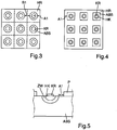
- the X-ray detector has three times three III-V semiconductor pixels, each pixel having a semiconductor contact region HK in the form of a mesa structure with an octagonal circumference and a top side covered by the respective rear connection contact KR.
- the semiconductor passivation layer HP completely encloses each semiconductor contact region HK at the minimum distance A1, so that a partial region of the top side of the absorption region is exposed around each semiconductor contact region HK.
- the semiconductor contact areas HK are each formed by implantation in the shape of a trough and with a circular top side in the common absorption area ABS.
- the rear connection contacts RK also have a circular circumference.
- the semiconductor passivation layer HP has a square recess in the area of each semiconductor contact region HK, the edge of the recess always having at least the minimum distance A1 from the respective semiconductor contact region.
- the III-V semiconductor pixel X-ray detector has an intermediate layer ZW between each semiconductor contact area HK and the common absorption area ABS, the intermediate layer having a conductivity type that corresponds to the semiconductor contact areas and a lower dopant concentration compared to the dopant concentration of the semiconductor contact areas.
- the semiconductor passivation layer HP has the minimum distance A1 from the intermediate layer ZW along the top side of the absorption region.
- the rear side connection contacts KR are each formed on a partial area of the top side of the respective semiconductor contact region HK.
- the x-ray detector does not have a further passivation layer P.
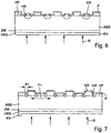
- the III-V semiconductor pixel X-ray detector has a highly doped semiconductor contact layer HKS of the first conductivity type between the absorption area ABS and the front-side connection contact KV, an upper side of the semiconductor contact layer HKS being materially connected to the underside of the absorption area ABS and an underside being materially connected to the front-side connection contact KV.
- An intermediate layer ZW of the first conductivity type is optionally (shown in dashed lines) between the semiconductor contact layer HKS and the absorption region, the top side of the semiconductor contact layer HKS being materially connected to the intermediate layer ZW and the intermediate layer ZW having a lower dopant concentration than the semiconductor contact layer HKS.
- the absorption area ABS has either the first or the second conductivity type, so that the pn junction is formed either between the semiconductor contact areas HK and the absorption area or between the semiconductor contact layer HKS and the absorption area.
Landscapes
- Physics & Mathematics (AREA)
- Health & Medical Sciences (AREA)
- Life Sciences & Earth Sciences (AREA)
- General Physics & Mathematics (AREA)
- High Energy & Nuclear Physics (AREA)
- Molecular Biology (AREA)
- Spectroscopy & Molecular Physics (AREA)
- Light Receiving Elements (AREA)
Abstract
Description
- Die Erfindung betrifft einen III-V-Halbleiterpixel-Röntgendetektor.
- Aus "A Method for Adjusting the Performance of Epitaxial GaAs X-ray Detectors", Sun, G.C. and Bourgoin, J.C., Nucl. Instrum. Methods Phys. Res., Sect. A, 2003, vol. 512, pp. 355-360, aus "GaAs Schottky versus p/i/n Diodes for Pixellated X-ray Detectors", Bourgoin, J.C. and Sun, G.C., Nucl. Instrum. Methods Phys. Res., Sect. A, 2002, vol. 487, pp. 47-49, ebenso aus der
DE 602 21 638 T2 , ist ein Verfahren und Gerät zur Herstellung eines GaAs-Detektors für eine Röntgenstrahl-Erfassung und eine Bildaufnahme bekannt. - Des Weiteren ist aus der
WO 2004 816 04 A2 - Als Pixel eines Röntgendetektors sind p-i-n Strukturen aus GaAs aus "GaAs Pixel-Detector Technology for X-ray Medical Imaging", Lezhneva et al.,a Russian Microelectronics, Vol. 34, No. 4, 2005, pp. 229-241, bekannt, wobei sowohl epitaktisch gewachsene als auch implantierte p+ Kontaktgebiet offenbart werden.
- Ein auf Schottky-Dioden basierender Röntgendetektor auf GaAs-Basis ist aus "GaAs X-Ray System Detectors for Medical Applications", Rizzi et al., https://www.researchgate.net/publication/237780321, bekannt.
- Nachteilig an den beschriebenen Strukturen sind die Rest- bzw. Leckströme, die bei einem Betrieb in Sperrrichtung, insbesondere über die Ränder der planaren p-n Übergänge bzw. der Mesa-Strukturen auftreten.
- Vor diesem Hintergrund besteht die Aufgabe der Erfindung darin, eine Vorrichtung anzugeben, die den Stand der Technik weiterbildet.
- Die Aufgabe wird durch einen III-V-Halbleiterpixel-Röntgendetektor mit den Merkmalen des Patentanspruchs 1 oder des Patentanspruchs 2 gelöst. Vorteilhafte Ausgestaltungen der Erfindung sind Gegenstand von Unteransprüchen.
- Gemäß dem Gegenstand der Erfindung wird ein III-V-Halbleiterpixel-Röntgendetektor bereitgestellt.
- In einer ersten alternativen Ausführungsform weist der III-V-Halbleiterpixel-Röntgendetektor ein Absorptionsgebiet eines ersten Leitfähigkeitstyps mit einer Oberseite und einer Unterseite sowie mindestens neun in einer Matrix entlang der Oberseite des Absorptionsgebiets angeordnete Halbleiterkontaktgebiete eines zweiten Leitfähigkeitstyps und mit einer ersten Energiebandlücke auf.
- Außerdem umfasst der III-V-Halbleiterpixel-Röntgendetektor einen unterhalb der Unterseite des Absorptionsgebiets angeordneten metallischen Vorderseitenanschlusskontakt und jeweils oberhalb jedes Halbleiterkontaktgebiets einen angeordneten metallischen Rückseitenanschlusskontakt.
- Des Weiteren weist der Röntgendetektor eine zu dem Absorptionsgebiet gitterangepasste Halbleiterpassivierungsschicht des ersten oder des zweiten Leitfähigkeitstyps und mit einer sich von der ersten Energiebandlücke der Halbleiterkontaktgebiete unterscheidenden Energiebandlücke auf.
- Die Halbleiterpassivierungsschicht ist gebietsweise auf der Oberseite des Absorptionsgebiets angeordnet und weist zu jedem hochdotierten Hableiterkontaktgebiet entlang der Oberseite des Absorptionsgebiets einen Mindestabstand von mindestens 2 µm oder von mindestens 10 µm oder von mindestens 20 µm oder von mindestens 40 µm auf.
- Eine zweite alternative Ausführungsform unterscheidet sich von der ersten Ausführungsform dahingehend, dass das Absorptionsgebiet den ersten Leitfähigkeitstyp oder den zweiten Leitfähigkeitstyp aufweist und der III-V-Halbleiterpixel-Röntgendetektor zusätzlich eine unterhalb der Unterseite des Absorptionsgebiets und oberhalb des metallischen Vorderseitenanschlusskontakts angeordnete Halbleiterkontaktschicht des ersten Leitfähigkeitstyps aufweist.
- Die Halbleiterkontaktschicht weist bevorzugt eine Dotierstoffkonzentration von mindestens 1•1017 cm-3 und eine Schichtdicke von 0,5 µm - 150 µm oder von 0,5 µm - 50 µm oder von 0,5 µm - 10 µm oder von 0,5 µm - 5 µm auf.
- Vorzugsweise beträgt der Mindestabstand der Halbleiterpassivierungsschicht zu jedem hochdotierten Halbleiterkontaktgebiet nicht mehr als eine Schichtdicke des Absorptionsgebiets.
- Es versteht sich, dass der Röntgendetektor dazu ausgelegt ist, insbesondere auf die Unterseite auftreffende Röntgenstrahlen zu detektieren.
- Das Absorptionsgebiet und die Halbleiterpassivierungsschicht sowie, wenn vorhanden die Halbleiterkontaktschicht, sind vorzugsweise epitaktisch erzeugt. Die Schichten werden vorzugsweise nacheinander auf einem Aufwachssubstrat aufgewachsen.
- Als Aufwachssubstrat eignet sich beispielsweise ein GaAs-Substrat oder ein Ge-Substrat, z.B. mit einer InGaAs-Schicht mit ca. 1 Prozent In zum Ausgleichen eines Gitterkonstantenunterschieds zwischen Germanium und Galliumarsenid. Das Aufwachssubstrat umfasst In einer anderen Ausführungsform eine Substratschicht sowie eine Pufferschicht.
- Die Pufferschicht dient zum Ausgleich eines Unterschieds zwischen den Gitterkonstanten von Substrat und aktiven Epitaxie-Schichten. Um GaAs-Schichten auf einem Ge-Substrat aufzuwachsen wird beispielsweise eine InGaAs-Pufferschicht mit einem sich schrittweise oder kontinuierlich Ändernden In Anteil verwendet.
- Das Aufwachssubstrat, also z.B. das GaAs-Substrat oder das Ge-Substrat und/oder eine Pufferschicht, wird anschließend durch Schleifen und / oder Ätzen und / oder andere Prozesse, z.B. Ablösen, bevorzugt vollständig gegebenenfalls auch nur teilweise entfernt.
- Beispielsweise wird in einem ersten Ätzschritt das Ge-Substrat entfernt, wobei die Pufferschicht als Ätzstoppschicht dient, und danach mittels eines weiteren Ätzprozesses, z.B. jeweils nasschemisches Ätzen, die Pufferschicht von dem photonischen GaAs-Bauelement entfernt.
- Alternativ wird das Aufwachssubstrat oder das Aufwachssubstrat sowie die Pufferschicht mittels eines kombinierten Schleif- und nachgeschalteten Ätzprozess entfernt. So kann der Großteil des Materialabtrags mittels Schleifen vorgenommen werden.
- In einer weiteren Ausführungsform wird während eines Herstellprozesses des stapelförmigen III-V-Halbleiterbauelements eine zusätzliche Ätzstoppschicht unterhalb des Absorptionsgebiets oder, wenn vorhanden, unterhalb der Halbleiterkontaktschicht eingefügt.
- Die Ätzstoppschicht wird beispielsweise zwischen dem Absorptionsgebiet und einer Pufferschicht oder einer Substratschicht oder zwischen der Halbleiterkontaktschicht und einer Pufferschicht oder einer Substratschicht oder zwischen einer Pufferschicht und einer Substratschicht erzeugt.
- Die Ätzstoppschicht ermöglicht ein sehr kontrolliertes Ablösen der Substratschicht und/oder der Pufferschicht oder nur der Substratschicht mittels eines Ätzprozesses, z.B. nasschemisches Ätzen.
- Insbesondere ermöglicht es die Ätzstoppschicht, Substrat und/oder Pufferschicht gegebenenfalls ganz ohne einen mechanischen Schleifprozess und sehr kontrolliert zu entfernen. Alternativ wird der Großteil des Substrats durch Schleifen entfernt und der verbleibende Rest durch nasschemisches Ätzen bis zu der Ätzstoppschicht.
- Die Ätzstoppschicht selbst kann danach auch entfernt werden. Die Ätzstoppschicht weist eine starke chemische Anisotropie gegenüber den angrenzenden Schichten auf, das heißt die Ätzrate für die Ätzstoppschicht und die anschließende Schicht unterscheiden sich mindestens um einen Faktor 10.
- Die Ätzstoppschicht besteht üblicherweise aus GaInP oder AlGaAs und die umgebenden Schichten aus GaAs oder GaInAs. Die entfernten Schichten sind in dem finalen Bauelement nicht mehr vorhanden.
- Alternativ zu dem vollständigen Entfernen des Aufwachssubstrats wird das Aufwachssubstrat, z.B. ein mit dem zweiten Leitfähigkeitstyp dotiertes GaAs-Substrat, nur teilweise entfernt, so dass eine verbleibende dünne Schicht hochdotierte Halbleiterkontaktschicht ausbildet.
- Die Halbleiterkontaktgebiete sind in einer ersten alternativen Ausführungsform als wannenförmige, in das Absorptionsgebiet hinein ragende Gebiete ausgebildet und beispielsweise durch eine Implantation erzeugt.
- In einer anderen alternativen Ausführungsform sind die Halbleiterkontaktgebiete jeweils als Mesa-Struktur ausgebildet. Vorzugsweise sind die Mesa-Strukturen oberhalb der Oberseite des Absorptionsgebiets angeordnet und beispielsweise mittels wenigstens eines Maskenprozesses sowie mittels Ätz- und Abscheideprozessen erzeugt sind.
- In einer Weiterbildung sind die Mesa-Strukturen auf dem Absorptionsgebiet angeordnet.
- In einer Weiterbildung sind die Mesa-Strukturen jeweils auf einer Zwischenschicht ausgebildet, wobei die jeweiligen Zwischenschichten die jeweiligen Halbleiterkontaktgebiete von dem gemeinsamen Absorptionsgebiet beabstanden.
- Es versteht sich auch, dass nur die Halbleitergebiete des Röntgendetektors, also insbesondere das Absorptionsgebiet, das Halbleiterkontaktgebiet und die Halbleiterpassivierungsschicht des Röntgendetektors sowie, wenn vorhanden die Halbleiterkontaktschicht, aus III-V-Materialien, z.B. GaAs, InGaP, InGaAs, AlGaAs oder InP, bestehen oder die vorgenannten III-V-Materialien umfassen.
- In einer ersten Ausführungsform weist der Röntgendetektor nur III-V-Halbleiterschichten auf. In einer Weiterbildung umfassen alle Halbleitergebiete GaAs oder InGaAs oder bestehen aus GaAs oder InGaAs.
- In einer weiteren Ausführungsform weist der Röntgendetektor zusätzliche Halbleiterschichten aus anderen Halbleitermaterialien oder zusätzliche Schichten aus anderen nicht-Halbleiter-Materialien, z.B. eine Nitridschicht und / oder eine Oxidschicht und / oder eine Oxynitridschicht und / oder eine Polyimidschicht als weitere Passivierungsschicht, auf.
- Es sei angemerkt, dass mit dem Ausdruck "besteht aus" eine Verbindung aus den genannten Stoffen ohne weitere III-V Elemente verstanden wird, jedoch Dotierstoffe, wie beispielsweise Zink oder Silizium oder Zinn oder Kohlenstoff, und auch gegebenenfalls Verunreinigungen und auch Störstellen umfasst sind. Folglich bedeutet beispielsweise "besteht aus GaAs", dass als III-V Elementen ausschließlich Gallium und Arsen jedoch nicht In oder Al oder P usw. eingebaut sind.
- Der Ausdruck "umfasst" bedeutet entsprechend, dass die genannten III-V Elemente, beispielsweise GaAs, enthalten sind und weitere III-V Elemente, wie beispielsweise Phosphor, Aluminium oder Indium, zusätzlich zu eventuellen Dotierstoffen und/oder Verunreinigungen und/oder Störstellen enthalten sein können.
- Die metallischen Anschlusskontakte bestehen in einer ersten alternativen Ausführungsform aus einer oder mehreren Metallschichten, z.B. Au und/oder Ag und/oder Pb und/oder Ge umfassende Schichten.
- Der metallische Vorderseitenanschlusskontakt ist in Ausführungsformen flächig oder fingerförmig oder punktförmig ausgebildet, wobei angemerkt wird, dass ein flächiger, beispielsweise schichtförmig die Unterseite des Absorptionsgebiets bedeckender Vorderseitenanschlusskontakt eine möglichst geringe Schichtdicke, insbesondere eine Schichtdicke von 5 nm - 2 µm oder von 10 nm - 1 µm aufweist, um eine Absorption von Röntgenstrahlen klein zu halten.
- Der Vorderseitenanschlusskontakt ist in einer anderen Ausführungsform stoffschlüssig mit der Unterseite des Absorptionsgebiets bzw., wenn vorhanden, stoffschlüssig mit der Unterseite der Halbleiterkontaktschicht verbunden.
- Alternativ ist der Vorderseitenanschlusskontakt stoffschlüssig mit einer zwischen dem Vorderseitenanschlusskontakt und dem Absorptionsgebiet angeordneten weiteren Halbleiterschicht verbunden.
- Die weitere Halbleiterschicht ist beispielsweise eine hochdotierte Halbleiterkontaktschicht mit Schichtdicken zwischen 1 µm bis 50 µm oder zwischen 1 µm - 20 µm.
- Es sei angemerkt, dass der matrixartige Röntgendetektor vorzugsweise einen kreisförmigen oder viereckigen, insbesondere rechteckigen oder quadratischen, Umfang aufweist, wobei ein Vereinzeln vorzugsweise durch Sägen erfolgt.
- Weiter versteht es sich, dass der erste Leitfähigkeitstyp n ist und der zweite Leitfähigkeitstyp p ist oder dass der erste Leitfähigkeitstyp p ist und der zweite Leitfähigkeitstyp n ist.
- Der III-V-Halbleiterpixel-Röntgendetektor Ist somit als n-auf-p oder als p-auf-n Struktur ausgebildet.
- Der Mindestabstand der Halbleiterpassivierungsschicht dient zusammen mit der Halbleiterpassivierungsschicht selbst der Unterdrückung von Leckströmen.
- Durch den bestehenden Abstand zwischen der Passivierungsschicht und dem Halbleiterkontaktgebiet, treten auch bei hohen Sperrspannungen oberhalb von 400 V nur besonders niedrige Sperrströme von kleiner 1 µA auf. Insbesondere liegen die Sperrströme in einem Bereich zwischen 0,5 nA und 50 nA oder unterhalb von 100 nA.
- Vorzugsweise beträgt der Mindestabstand zu den Halbleiterkontaktschichten mindestens 50% oder mindestens 75% der Schichtdicke des Absorptionsgebiets.
- Vorteile der erfindungsgemäßen Halbleiterdetektorstruktur sind ein besonders geringer Sperrstrom und eine hohe Durchbruchspannung. Insbesondere weist die Durchbruchkennlinie einen nahezu idealen Verlauf auf. Der besonders niedrige Sperrstrom ermöglicht das Anlegen hoher Rückwärtsspannungen, wodurch eine sehr hohe Empfindlichkeit erreicht wird.
- Untersuchungen haben gezeigt, dass die Durchbruchspannung auch von dem Mindestabstand zwischen der Halbleiterpassivierungsschicht und den Halbleiterkontaktgebieten bestimmt wird. Mit dem erfindungsgemäßen Röntgendetektor lassen sich Durchbruchfeldstärken von bis zu 40 V/µm und sehr zuverlässig Durchbruchfeldstärken von über 30 V/µm erreichen.
- III-V-Materialien, insbesondere GaAs, ermöglichen aufgrund einer hohen Ladungsträgerbeweglichkeit zusätzlich eine besonders empfindliche bzw. effiziente Detektion von Röntgenstrahlen, insbesondere von niederenergetischen Röntgenstrahlen.
- Ein Vorteil des erfindungsgemäßen Röntgendetektors ist daher die große Empfindlichkeit, wodurch eine Reduktion der notwenigen Dosis, der beispielsweise ein Patient ausgesetzt werden muss, möglich ist.
- Ebenso ist aufgrund der hohen Beweglichkeit der Ladungsträger nur eine sehr kurze Zeit pro Bildaufnahme nötig, was zu einer geringen Strahlenbelastung führt. Weiterhin ermöglicht die hohe Ladungsträgerbeweglichkeit farbiges Röntgen basierend auf "Photon Counting".
- Das erfindungsgemäße Bauelement ist außerdem in verhältnismäßig wenigen Prozessschritten und dadurch relativ kostengünstig oder zumindest mit vertretbaren Kosten herstellbar.
- In einer weiteren Ausführungsform ist zwischen dem Absorptionsgebiet und jedem Halbleiterkontaktgebiet jeweils eine Zwischenschicht des zweiten Leitfähigkeitstyps ausgebildet, wobei die Halbleiterpassivierungsschicht zu jeder Zwischenschicht entlang der Oberseite des Absorptionsgebiets den Mindestabstand aufweist.
- Ist die Halbleiterkontaktschicht unterhalb des Absorptionsgebiets vorhanden, so ist In einer anderen Weiterbildung zwischen dem Absorptionsgebiets und der Halbleiterkontaktschicht eine Zwischenschicht des ersten Leitfähigkeitstyps ausgebildet.
- Die Zwischenschichten weisen jeweils vorzugsweise eine geringere Dotierstoffkonzentration als der angrenzenden Halbleiterkontaktbereich, also das Halbleiterkontaktgebiets bzw. die Halbleiterschicht, auf.
- Außerdem werden die Zwischenschichten jeweils vorzugsweise auf dieselbe Weise erzeugt, wie das Halbleiterkontaktgebiet bzw. die Halbleiterkontaktschicht, also beispielsweise durch Implantation oder als Mesa-Struktur durch Abscheide- und Ätzprozesse bzw. als epitaktische Schicht.
- Es versteht sich, dass sich die Zwischenschichten nicht ausschließen. Der III-V-Halbleiterpixel-Röntgendetektor kann eine der beiden Zwischenschichten oder auch beide Zwischenschichten aufweisen.
- In einer anderen Ausführungsform weist das Absorptionsgebiet eine Dotierstoffkonzentration von 8•1011 - 1•1014 cm-3, also eine geringe Dotierung, und/oder eine Schichtdicke von 80 µm - 2000 µm oder von 500 µm - 2000 µm oder von 900 µm - 2000 µm auf.
- Mit dem besonders tiefen Absorptionsgebiet zur Absorption und der durch die beabstandete Halbleiterpassivierungsschicht besonders hohen Sperrspannung eignet sich die erfindungsgemäße Halbleiterstruktur besonders zur Strahlungsdetektion.
- Die Halbleiterkontaktgebiete weisen jeweils vorzugsweise eine Dotierstoffkonzentration von mindestens 5•1018 cm-3 auf, sind also hochdotiert.
- In einer Weiterbildung beträgt der Mindestabstand mindestens 50 µm oder mindestens 100 µm oder mindestens 1000 µm.
- In einer anderen Weiterbildung weisen die Halbleiterkontaktgebiete jeweils von Mitte zu Mitte einen Abstand von mindestens 20 µm oder von mindestens 50 µm auf.
- Es versteht sich, dass der Abstand der Halbleiterkontaktgebiete den Pixelabstand bzw. Bildpunktabstand bzw. Pixel-Pitch vorgibt. Vorzugsweise ist der Abstand auf eine Auswerteeinheit abgestimmt, insbesondere um mittels Flip-Chip-Technologie mit einer entsprechenden Auswerteeinheit verbunden werden zu können.
- In einer weiteren Ausführungsform weist die Halbleiterpassivierungsschicht eine Schichtdicke von 0,1 µm - 1 µm auf. Außerdem umfasst die Halbleiterpassivierungsschicht eine Verbindung aus InGaP und / oder AlGaAs und/oder InGaAsP auf oder besteht aus AlGaAs oder aus InGaP oder aus InGaAsP.
- In einer anderen Weiterbildung umschließt die Halbleiterpassivierungsschicht in einer Projektion senkrecht zu der Oberseite des Absorptionsgebiets die Halbleiterkontaktgebiete oder zumindest einige der Halbleiterkontaktgebiete jeweils vollständig.
- In einer weiteren Weiterbildung weisen die Halbleiterkontaktgebiete und das Absorptionsgebiet jeweils GaAs auf oder bestehen aus GaAs.
- Die Erfindung wird nachfolgend unter Bezugnahme auf die Zeichnungen näher erläutert. Hierbei werden gleichartige Teile mit identischen Bezeichnungen beschriftet.
- Die dargestellten Ausführungsformen sind stark schematisiert, d.h. die Abstände und die lateralen und die vertikalen Erstreckungen sind nicht maßstäblich und weisen, sofern nicht anders angegeben, auch keine ableitbaren geometrischen Relationen zueinander auf. Darin zeigen, die
- Figur 1
- einen Querschnitt einer ersten Ausführungsform eines III-V-Halbleiterpixel-Röntgendetektors,
- Figur 2
- einen Querschnitt einer zweiten Ausführungsform des III-V-Halbleiterpixel-Röntgendetektors,
- Figur 3
- eine Aufsicht auf eine weitere Ausführungsform des III-V-Halbleiterpixel-Röntgendetektors,
- Figur 4
- eine Aufsicht auf eine weitere Ausführungsform des III-V-Halbleiterpixel-Röntgendetektors,
- Figur 5
- einen Querschnitt einer weiteren Ausführungsform eines III-V-Halbleiterpixels des Röntgendetektors,
- Figur 6
- einen Querschnitt einer weiteren Ausführungsform des III-V-Halbleiterpixel-Röntgendetektors,
- Figur 7
- einen Querschnitt einer weiteren Ausführungsform des III-V-Halbleiterpixel-Röntgendetektors.
- Die Abbildung der
Figur 1 zeigt einen Querschnitt einer ersten erfindungsgemäßen Ausführungsform eines III-V-Halbleiterpixel-Röntgendetektors zur Detektion von Röntgenstrahlen R. - Der Röntgendetektor weist eine Matrix von vier mal vier III-V-Halbleiterpixel auf. Es sei angemerkt, dass die Matrix in einer nicht dargestellten Ausführungsform drei mal drei III-V-Halbleiterpixel aufweist. Es versteht sich, dass in einer anderen nicht dargestellten Ausführungsform der Röntgendetektor mehr als sechszehn III-V-Halbleiterpixel aufweist.
- Die Halbleiterpixel umfassen ein gemeinsames Absorptionsgebiet ABS mit einer Unterseite, einer Oberseite und einer Schichtdicke D1 sowie einen gemeinsamen Vorderseitenanschlusskontakt KV, wobei der Vorderseitenanschlusskontakt als Metallschicht mit möglichst geringer Schichtdicke D2 ausgebildet ist und die Unterseite des Absorptionsgebiets ABS bedeckt und mit der Unterseite des Absorptionsgebiets ABS stoffschlüssig verbunden ist.
- Jeder Halbleiterpixel umfasst außerdem ein Halbleiterkontaktgebiet HK, wobei die Halbleiterkontaktgebiete HK sich jeweils von einer Oberseite wannenförmig bis zu einer Tiefe T1 in das Absorptionsgebiet ABS hinein erstrecken. Benachbarte Halbeiterkontaktgebiete HK weisen von Mitte zu Mitte einen Abstand P1 auf, wobei der Abstand P1 dem Pixel Pitch bzw. dem Bildpunktabstand entspricht.
- Zwischen den Halbleiterkontaktgebieten HK ist auf der Oberseite des Absorptionsgebiets ABS jeweils eine Halbleiterpassivierungsschicht HP mit einer Schichtdicke D3 angeordnet, wobei die Halbleiterpassivierungsschicht HP mit der Oberseite des Absorptionsgebiets ABS stoffschlüssig verbunden Ist und zu jedem der Halbleiterkontaktgebiete jeweils einen Mindestabstand A1 von mindestens 2 µm aufweist.
- Eine Oberseite der Halbleiterpassivierungsschicht HP sowie ein zwischen der Halbleiterpassivierungsschicht HP und dem Halbleiterkontaktgebieten HK liegender Teilbereich der Oberseite des Absorptionsgebiets ABS und jeweils ein an die Oberseite des Absorptionsgebiets angrenzender Randbereich der Halbleiterkontaktgebiete HK ist optional von einer weiteren Passivierungsschicht P, z.B. einer dünnen Siliziumnitrid oder Oxidschicht bedeckt (gestrichelt dargestellt).
- Auf der Oberseite jedes Halbleiterkontaktgebiets HK ist jeweils ein Rückseitenanschlusskontakt KR angeordnet, wobei sich jeder Rückseitenanschlusskontakt KR jeweils auch über einen angrenzenden Bereich der weiteren Passivierungsschicht P erstreckt, wenn die weitere Passivierungsschicht P vorhanden ist und mit der jeweiligen Oberseite des Halbleiterkontaktgebiets HK und gegebenenfalls der weiteren Passivierungsschicht P stoffschlüssig verbunden ist.
- In der Abbildung der
Figur 2 ist eine weitere Ausführungsform dargestellt. Im Folgenden werden nur die Unterschiede zu der Abbildung derFigur 1 erläutert. - Die Halbleiterkontaktgebiete HK sind jeweils als Mesa-Struktur auf einem jeweiligen Teilbereich der Oberseite des Absorptionsgebiets ABS angeordnet, wobei die Rückseitenanschlusskontakte KR jeweils flächig auf eine Oberseite der jeweiligen Mesa-Struktur ausgebildet sind.
- Der Röntgendetektor weist keine weitere Passivierungsschicht P auf. Der gemeinsame Rückseitenanschlusskontakt RK ist punktförmig bzw. nur auf einem kleinen Teilbereich der Unterseite des Absorptionsgebiets ABS ausgebildet.
- In der Abbildung der
Figur 3 ist eine Aufsicht auf eine weitere Ausführungsform des Röntgendetektors ausgebildet. - Der Röntgendetektor weist dreimal drei III-V-Halbleiterpixel auf, wobei jeder Pixel ein als Mesa-Struktur ausgebildetes Halbleiterkontaktgebiet HK mit einem achteckigen Umfang und einer von dem jeweiligen Rückseitenanschlusskontakt KR bedeckten Oberseite aufweist.
- Die Halbleiterpassivierungsschicht HP umschließt jedes Halbleiterkontaktgebiet HK vollständig in dem Mindestabstand A1, so dass um jedes Halbleiterkontaktgebiet HK ein Teilbereich der Oberseite des Absorptionsgebiets frei liegt.
- In der Abbildung der
Figur 3 ist eine Aufsicht einer weiteren Ausführungsform dargestellt. Im Folgenden werden nur die Unterschiede zu der Abbildung derFigur 3 erläutert. - Die Halbleiterkontaktgebiet HK sind jeweils durch Implantation wannenförmig und mit kreisförmiger Oberseite in dem gemeinsamen Absorptionsgebiet ABS ausgebildet. Die Rückseitenanschlusskontakte RK weisen ebenfalls einen kreisförmigen Umfang auf.
- Die Halbleiterpassivierungsschicht HP weist im Bereich jedes Halbleiterkontaktgebiets HK eine quadratische Ausnehmung auf, wobei der Rand der Ausnehmung zu dem jeweiligen Halbleiterkontaktgebiet immer mindestens den Mindestabstand A1 aufweist.
- In der Abbildung der
Figur 5 ist eine weitere Ausführungsform eines Ausschnitts eines III-V-Halbleiterpixel-Röntgendetektors dargestellt. Im Folgenden werden nur die Unterschiede zu der Abbildung derFigur 1 erläutert. - Der III-V-Halbleiterpixel-Röntgendetektor weist zwischen jedem Halbleiterkontaktgebiet HK und dem gemeinsamen Absorptionsgebiet ABS jeweils eine Zwischenschicht ZW auf, wobei die Zwischenschicht einen mit den Halbleiterkontaktgebieten übereinstimmenden Leitfähigkeitstyp und eine im Vergleich zu der Dotierstoffkonzentration der Halbleiterkontaktgebiete geringeren Dotierstoffkonzentration aufweist.
- Die Halbleiterpassivierungsschicht HP weist zu der Zwischenschicht ZW entlang der Oberseite des Absorptionsgebiets den Mindestabstand A1 auf.
- Die Rückseitenanschlusskontakte KR sind jeweils auf einem Teilbereich der Oberseite des jeweiligen Halbleiterkontaktgebiets HK ausgebildet. Eine weitere Passivierungsschicht P weist der Röntgendetektor nicht auf.
- In den Abbildungen der
Figuren 6 ist jeweils eine weitere Ausführungsform eines Ausschnitts eines III-V-Halbleiterpixel-Röntgendetektors dargestellt. Im Folgenden werden nur die Unterschiede zu der Abbildung derFigur 1 bzw. der Abbildung derFigur 2 erläutert. - Der III-V-Halbleiterpixel-Röntgendetektor weist zwischen dem Absorptionsgebiet ABS und dem Vorderseitenanschlusskontakt KV eine hochdotierte Halbleiterkontaktschicht HKS des ersten Leitfähigkeitstyps auf, wobei eine Oberseite der Halbleiterkontaktschicht HKS stoffschlüssig mit der Unterseite des Absorptionsgebiets ABS und eine Unterseite stoffschlüssig mit dem Vorderseitenanschlusskontakt KV verbunden ist.
- Optional (jeweils gestrichelt eingezeichnet) ist zwischen der Halbleiterkontaktschicht HKS und dem Absorptionsgebiet eine Zwischenschicht ZW des ersten Leitfähigkeitstyps angeordnet, wobei die Oberseite der Halbleiterkontaktschicht HKS stoffschlüssig mit der Zwischenschicht ZW verbunden ist und die Zwischenschicht ZW eine niedrigere Dotierstoffkonzentration als die Halbleiterkontaktschicht HKS aufweist.
- In den Ausführungsbeispielen der
Figuren 6 und 7 weist das Absorptionsgebiet ABS entweder den ersten oder den zweiten Leitfähigkeitstyp auf, so dass sich der p-n Übergang entweder zwischen den Halbleiterkontaktgebieten HK und dem Absorptionsgebiet oder zwischen der Halbleiterkontaktschicht HKS und dem Absorptionsgebiet ausbildet.
Claims (15)
- III-V-Halbleiterpixel-Röntgendetektor, aufweisend- ein Absorptionsgebiet (ABS) eines ersten Leitfähigkeitstyps mit einer Oberseite und einer Unterseite,- mindestens neun in einer Matrix entlang der Oberseite des Absorptionsgebiets (ABS) angeordnete Halbleiterkontaktgebiete (HK) eines zweiten Leitfähigkeitstyps und mit einer ersten Energiebandlücke, wobei- ein metallischer Vorderseitenanschlusskontakt (KV) unterhalb der Unterseite des Absorptionsgebiets (ABS) angeordnet ist und- oberhalb jedes Halbleiterkontaktgebiets (HK) jeweils ein metallischer Rückseitenanschlusskontakt (KR) angeordnet ist,
der Röntgendetektor eine Halbleiterpassivierungsschicht (HP) des ersten oder des zweiten Leitfähigkeitstyps und mit einer sich von der ersten Energiebandlücke unterscheidenden zweiten Energiebandlücke aufweist, wobei- die Halbleiterpassivierungsschicht (HP) und das Absorptionsgebiet (ABS) zueinander gitterangepasst sind,- die Halbleiterpassivierungsschicht (HP) gebietsweise auf der Oberseite des Absorptionsgebiets (ABS) angeordnet ist und- die Halbleiterpassivierungsschicht (HP) zu jedem Halbeiterkontaktgebiet (HK) entlang der Oberseite des Absorptionsgebiets (ABS) einen Mindestabstand (A1) von mindestens 2 µm oder von mindestens 10 µm oder von mindestens 20 µm oder von mindestens 40 µm aufweist. - III-V-Halbleiterpixel-Röntgendetektor, aufweisend- ein Absorptionsgebiet (ABS) eines ersten oder eines zweiten Leitfähigkeitstyps mit einer Oberseite und einer Unterseite,- mindestens neun in einer Matrix entlang der Oberseite des Absorptionsgebiets (ABS) angeordnete Halbleiterkontaktgebiete (HKG) des zweiten Leitfähigkeitstyps und mit einer ersten Energiebandlücke,- eine Halbleiterkontaktschicht (HKS) des ersten Leitfähigkeitstyps, wobei- die Halbleiterkontaktschicht (HKS) unterhalb der Unterseite des Absorptionsgebiets (ABS) angeordnet ist,- ein metallischer Vorderseitenanschlusskontakt (KV) unterhalb einer Unterseite der Halbleiterkontaktschicht (HKS) angeordnet ist und- oberhalb jedes Halbleiterkontaktgebiets (HK) jeweils ein metallischer Rückseitenanschlusskontakt (KR) angeordnet ist,- der Röntgendetektor eine Halbleiterpassivierungsschicht (HP) des ersten oder des zweiten Leitfähigkeitstyps und mit einer sich von der ersten Energiebandlücke unterscheidenden zweiten Energiebandlücke aufweist, wobei- die Halbleiterpassivierungsschicht (HP) und das Absorptionsgebiet (ABS) zueinander gitterangepasst sind,- die Halbleiterpassivierungsschicht (HP) gebietsweise auf der Oberseite des Absorptionsgebiets (ABS) angeordnet ist und- die Halbleiterpassivierungsschicht (HP) zu jedem Halbeiterkontaktgebiet (HK) entlang der Oberseite des Absorptionsgebiets (ABS) einen Mindestabstand (A1) von mindestens 2 µm oder von mindestens 10 µm oder von mindestens 20 µm oder von mindestens 40 µm aufweist.
- III-V-Halbleiterpixel-Röntgendetektor nach Anspruch 2, dadurch gekennzeichnet, dass die Halbleiterkontaktschicht (HKS) eine Dotierstoffkonzentration von mindestens 1•1017 cm-3 und eine Schichtdicke von 0,5 µm - 150 µm oder von 0,5 µm - 50 µm oder von 0,5 µm - 10 µm oder von 0,5 µm - 5 µm aufweist.
- III-V-Halbleiterpixel-Röntgendetektor nach Anspruch 2 oder 3, dadurch gekennzeichnet, dass zwischen dem Absorptionsgebiet (ABS) und der Halbleiterkontaktschicht (HKS) eine Zwischenschicht (ZWS) des ersten Leitfähigkeitstyps ausgebildet ist.
- III-V-Halbleiterpixel-Röntgendetektor nach einem der vorstehenden Ansprüche, dadurch gekennzeichnet, dass zwischen dem Absorptionsgebiet (ABS) und jedem Halbleiterkontaktgebiet (HK) jeweils eine Zwischenschicht (ZW) des zweite Leitfähigkeitstyps ausgebildet ist, wobei die Halbleiterpassivierungsschicht (HP) zu jeder Zwischenschicht (ZW) entlang der Oberseite des Absorptionsgebiets (ABS) den Mindestabstand (A1) aufweist.
- III-V-Halbleiterpixel-Röntgendetektor nach einem der vorstehenden Ansprüche, dadurch gekennzeichnet, dass das Absorptionsgebiet (ABS) eine Dotierstoffkonzentration von 8•1011 - 1•1014 cm-3 und/oder eine Schichtdicke von 80 µm - 2000 µm oder von 500 µm - 2000 µm oder von 900 µm - 2000 µm aufweist.
- III-V-Halblelterpixel-Röntgendetektor nach einem der vorstehenden, dadurch gekennzeichnet, dass die Halbleiterkontaktgebiete (HK) jeweils eine Dotierstoffkonzentration von mindestens 5•1018 cm-3 aufweisen.
- III-V-Halbleiterpixel-Röntgendetektor nach einem der vorstehenden Ansprüche, dadurch gekennzeichnet, dass sich die Halbleiterkontaktgebiete (HK) jeweils von wannenförmig in das Absorptionsgebiet (ABS) hinein erstrecken.
- III-V-Halbleiterpixel-Röntgendetektor nach einem der Ansprüche 1 bis 7, dadurch gekennzeichnet, dass die Halbleiterkontaktgebiete (HK) jeweils als Mesa-Struktur oberhalb der Oberseite des Absorptionsgebiets (ABS) angeordnet sind.
- III-V-Halbleiterpixel-Röntgendetektor nach einem der vorstehenden Ansprüche, dadurch gekennzeichnet, dass der Mindestabstand (A1) mindestens 50 µm oder mindesten 100 µm oder mindestens 1000 µm beträgt.
- III-V-Halbleiterpixel-Röntgendetektor nach einem der vorstehenden Ansprüche, dadurch gekennzeichnet, dass die Halbleiterkontaktgebiete (HK) jeweils von Mitte zu Mitte einen Abstand von mindestens 20 µm oder von mindestens 50 µm aufweisen.
- III-V-Halbleiterpixel-Röntgendetektor nach einem der vorstehenden Ansprüche, dadurch gekennzeichnet, dass die Halbleiterpassivierungsschicht (HP) eine Schichtdicke (D3) von 0,1 µm - 1 µm aufweist.
- III-V-Halbleiterpixel-Röntgendetektor nach einem der vorstehenden Ansprüche, dadurch gekennzeichnet, dass die Halbleiterpassivierungsschicht (HP) InGaP und/oder AlGaAs und/oder InGaAsP aufweist oder aus InGaP oder AlGaAs oder InGaAsP besteht.
- III-V-Halbleiterpixel-Röntgendetektor nach einem der vorstehenden Ansprüche, dadurch gekennzeichnet, dass die Halbleiterpassivierungsschicht (HP) in einer Projektion senkrecht zu der Oberseite des Absorptionsgebiets (ABS) die Halbleiterkontaktgebiete (HK) oder zumindest einige der Halbleiterkontaktgebiete (HK) jeweils vollständig umschließt.
- III-V-Halbleiterpixel-Röntgendetektor nach einem der vorstehenden Ansprüche, dadurch gekennzeichnet, dass die Halbleiterkontaktgebiete (HK) und das Absorptionsgebiet (ABS) und so vorhanden die Halbleiterkontaktschicht (HKS) jeweils GaAs aufweisen oder aus GaAs bestehen.
Applications Claiming Priority (1)
| Application Number | Priority Date | Filing Date | Title |
|---|---|---|---|
| DE102020001839.4A DE102020001839B3 (de) | 2020-03-20 | 2020-03-20 | lll-V-Halbleiterpixel-Röntgendetektor |
Publications (2)
| Publication Number | Publication Date |
|---|---|
| EP3882671A1 true EP3882671A1 (de) | 2021-09-22 |
| EP3882671B1 EP3882671B1 (de) | 2025-09-24 |
Family
ID=74874612
Family Applications (1)
| Application Number | Title | Priority Date | Filing Date |
|---|---|---|---|
| EP21000068.3A Active EP3882671B1 (de) | 2020-03-20 | 2021-03-12 | Iii-v-halbleiterpixel-röntgendetektor |
Country Status (3)
| Country | Link |
|---|---|
| US (1) | US11594570B2 (de) |
| EP (1) | EP3882671B1 (de) |
| DE (1) | DE102020001839B3 (de) |
Families Citing this family (1)
| Publication number | Priority date | Publication date | Assignee | Title |
|---|---|---|---|---|
| CN114447149B (zh) * | 2022-01-11 | 2023-12-01 | 上海奕瑞光电子科技股份有限公司 | 一种边缘入射探测器及其制作方法 |
Citations (3)
| Publication number | Priority date | Publication date | Assignee | Title |
|---|---|---|---|---|
| WO2004081604A2 (fr) | 2003-03-04 | 2004-09-23 | Universite Pierre Et Marie Curie | Imageur x a conversion directe et son procede de fabrication |
| DE60221638T2 (de) | 2001-01-31 | 2008-05-08 | Universite Pierre Et Marie Curie | Verfahren und gerät zur herstellung eines gaas-detektors für röntgenstrahl- erfassung und bildaufnahme |
| US20150372047A1 (en) * | 2013-01-31 | 2015-12-24 | New Imaging Technologies | Photodiode array having a charge-absorbing doped region |
Family Cites Families (4)
| Publication number | Priority date | Publication date | Assignee | Title |
|---|---|---|---|---|
| US20080110489A1 (en) * | 2006-11-14 | 2008-05-15 | Fareed Sepehry-Fard | Very High Efficiency Multi-Junction Solar Spectrum Integrator Cells, and the Corresponding System and Method |
| US8237126B2 (en) * | 2007-08-17 | 2012-08-07 | Csem Centre Suisse D'electronique Et De Mictrotechnique Sa | X-ray imaging device and method for the manufacturing thereof |
| IL238368B (en) * | 2015-04-19 | 2019-08-29 | Semi Conductor Devices An Elbit Systems Rafael Partnership | light sensor |
| US10007007B2 (en) * | 2015-09-08 | 2018-06-26 | Shenzhen Xpectvision Technology Co., Ltd. | Methods for making an X-ray detector |
-
2020
- 2020-03-20 DE DE102020001839.4A patent/DE102020001839B3/de active Active
-
2021
- 2021-03-12 EP EP21000068.3A patent/EP3882671B1/de active Active
- 2021-03-22 US US17/209,144 patent/US11594570B2/en active Active
Patent Citations (3)
| Publication number | Priority date | Publication date | Assignee | Title |
|---|---|---|---|---|
| DE60221638T2 (de) | 2001-01-31 | 2008-05-08 | Universite Pierre Et Marie Curie | Verfahren und gerät zur herstellung eines gaas-detektors für röntgenstrahl- erfassung und bildaufnahme |
| WO2004081604A2 (fr) | 2003-03-04 | 2004-09-23 | Universite Pierre Et Marie Curie | Imageur x a conversion directe et son procede de fabrication |
| US20150372047A1 (en) * | 2013-01-31 | 2015-12-24 | New Imaging Technologies | Photodiode array having a charge-absorbing doped region |
Non-Patent Citations (5)
| Title |
|---|
| BOURGOIN, J.C.SUN, G.C.: "GaAs Schottky versus p/i/n Diodes for Pixellated X-ray Detectors", NUCL. INSTRUM. METHODS PHYS. RES., vol. 487, 2002, pages 47 - 49, XP004369000, DOI: 10.1016/S0168-9002(02)00943-9 |
| DVORYANKIN V F ET AL: "Multielement X-ray row detector on GaAs with spatial resolution of 108@mm", NUCLEAR INSTRUMENTS & METHODS IN PHYSICS RESEARCH. SECTION A, ELSEVIER BV * NORTH-HOLLAND, NL, vol. 531, no. 1-2, 21 September 2004 (2004-09-21), pages 87 - 88, XP004564749, ISSN: 0168-9002, DOI: 10.1016/J.NIMA.2004.05.097 * |
| LEZHNEVA ET AL.: "GaAs Pixel-Detector Technology for X-ray Medical Imaging", RUSSIAN MLCROELECTRONICS, vol. 34, no. 4, 2005, pages 229 - 241, XP019302363 |
| RIZZI ET AL., GAAS X-RAY SYSTEM DETECTORS FOR MEDICAL APPLICATIONS, Retrieved from the Internet <URL:https://www.researchgate.net/publication/237780321> |
| SUN, G.C.BOURGOIN, J.C.: "A Method for Adjusting the Performance of Epitaxial GaAs X-ray Detectors", NUCL. INSTRUM. METHODS PHYS. RES., vol. 512, 2003, pages 355 - 360 |
Also Published As
| Publication number | Publication date |
|---|---|
| US11594570B2 (en) | 2023-02-28 |
| US20210296391A1 (en) | 2021-09-23 |
| EP3882671B1 (de) | 2025-09-24 |
| DE102020001839B3 (de) | 2021-09-23 |
Similar Documents
| Publication | Publication Date | Title |
|---|---|---|
| DE112010005626B4 (de) | Halbleitervorrichtung | |
| DE102009038731B4 (de) | Halbleiterbauelement mit Ladungsträgerkompensationsstruktur und Verfahren zur Herstellung eines Halbleiterbauelements | |
| DE2711562C3 (de) | Halbleiterbauelement und Verfahren zu seiner Herstellung | |
| DE112013004533B4 (de) | Siliziumkarbid-Halbleitereinrichtung mit Sperrschicht-Schottky-Diode | |
| DE69601981T2 (de) | Herstellungsverfahren einer halbleiteranordnung aus siliziumkarbid | |
| DE69802739T2 (de) | Avalanche-Photodiode und Methode zu deren Herstellung | |
| DE102016108125B4 (de) | Halbleitervorrichtung und Herstellung davon | |
| DE102009017505B4 (de) | Strahlungsdetektor, Verwendung eines Strahlungsdetektors und Verfahren zur Herstellung eines Strahlungsdetektors | |
| DE102020001839B3 (de) | lll-V-Halbleiterpixel-Röntgendetektor | |
| DE102014116631B4 (de) | Junction-feldeffekttransistorzelle mit lateralem kanalbereich | |
| EP3734667B1 (de) | Stapelförmige hochsperrende iii-v-halbleiterleistungsdiode | |
| EP3734668B1 (de) | Stapelförmige hochsperrende ingaas-halbleiterleistungsdiode | |
| DE102019135490B4 (de) | Ionenstrahl-implantationsverfahren | |
| DE102015118315B4 (de) | Halbleitervorrichtung mit Tiefdiffusionsregion | |
| DE102021200828A1 (de) | Fotodiode mit orthogonalem Schichtaufbau | |
| DE102020001840B3 (de) | Stapelförmiges photonisches III-V-Halbleiterbauelement | |
| DE102016112111B4 (de) | Superjunction-halbleitervorrichtung | |
| DE102020001837B3 (de) | Stapelförmiges photonisches lll-V-Halbleiterbauelement | |
| DE102017106202A1 (de) | Verfahren zum herstellen einer halbleitervorrichtung, umfassend eine ätzung eines halbleitermaterials | |
| DE102020001844B3 (de) | Stapelförmiges photonisches lll-V-Halbleiterbauelement | |
| DE10308626B4 (de) | Verfahren zur Herstellung von Halbleiter-Strahlungsdetektoren und Halbleiter-Strahlungsdetektor | |
| EP3882982A1 (de) | Stapelförmiges photonisches iii-v-halbleiterbauelement | |
| DE102020001841B4 (de) | Stapelförmige hochsperrende III-V-Halbleiterleistungsdiode | |
| DE102019001459B3 (de) | Stapelförmige hochsperrende III-V-Leistungshalbleiterdiode | |
| DE102004047313B3 (de) | Halbleiteranordnung mit einem Tunnelkontakt und Verfahren zu deren Herstellung |
Legal Events
| Date | Code | Title | Description |
|---|---|---|---|
| PUAI | Public reference made under article 153(3) epc to a published international application that has entered the european phase |
Free format text: ORIGINAL CODE: 0009012 |
|
| STAA | Information on the status of an ep patent application or granted ep patent |
Free format text: STATUS: REQUEST FOR EXAMINATION WAS MADE |
|
| 17P | Request for examination filed |
Effective date: 20210713 |
|
| AK | Designated contracting states |
Kind code of ref document: A1 Designated state(s): AL AT BE BG CH CY CZ DE DK EE ES FI FR GB GR HR HU IE IS IT LI LT LU LV MC MK MT NL NO PL PT RO RS SE SI SK SM TR |
|
| STAA | Information on the status of an ep patent application or granted ep patent |
Free format text: STATUS: EXAMINATION IS IN PROGRESS |
|
| 17Q | First examination report despatched |
Effective date: 20220927 |
|
| GRAP | Despatch of communication of intention to grant a patent |
Free format text: ORIGINAL CODE: EPIDOSNIGR1 |
|
| STAA | Information on the status of an ep patent application or granted ep patent |
Free format text: STATUS: GRANT OF PATENT IS INTENDED |
|
| RIC1 | Information provided on ipc code assigned before grant |
Ipc: G01T 1/24 20060101AFI20250616BHEP |
|
| INTG | Intention to grant announced |
Effective date: 20250708 |
|
| GRAS | Grant fee paid |
Free format text: ORIGINAL CODE: EPIDOSNIGR3 |
|
| GRAA | (expected) grant |
Free format text: ORIGINAL CODE: 0009210 |
|
| STAA | Information on the status of an ep patent application or granted ep patent |
Free format text: STATUS: THE PATENT HAS BEEN GRANTED |
|
| AK | Designated contracting states |
Kind code of ref document: B1 Designated state(s): AL AT BE BG CH CY CZ DE DK EE ES FI FR GB GR HR HU IE IS IT LI LT LU LV MC MK MT NL NO PL PT RO RS SE SI SK SM TR |
|
| REG | Reference to a national code |
Ref country code: GB Ref legal event code: FG4D Free format text: NOT ENGLISH |
|
| REG | Reference to a national code |
Ref country code: CH Ref legal event code: EP |
|
| REG | Reference to a national code |
Ref country code: DE Ref legal event code: R096 Ref document number: 502021008756 Country of ref document: DE |
|
| REG | Reference to a national code |
Ref country code: IE Ref legal event code: FG4D Free format text: LANGUAGE OF EP DOCUMENT: GERMAN |
|
| PG25 | Lapsed in a contracting state [announced via postgrant information from national office to epo] |
Ref country code: NO Free format text: LAPSE BECAUSE OF FAILURE TO SUBMIT A TRANSLATION OF THE DESCRIPTION OR TO PAY THE FEE WITHIN THE PRESCRIBED TIME-LIMIT Effective date: 20251224 |
|
| REG | Reference to a national code |
Ref country code: LT Ref legal event code: MG9D |
|
| PG25 | Lapsed in a contracting state [announced via postgrant information from national office to epo] |
Ref country code: FI Free format text: LAPSE BECAUSE OF FAILURE TO SUBMIT A TRANSLATION OF THE DESCRIPTION OR TO PAY THE FEE WITHIN THE PRESCRIBED TIME-LIMIT Effective date: 20250924 |
|
| PG25 | Lapsed in a contracting state [announced via postgrant information from national office to epo] |
Ref country code: HR Free format text: LAPSE BECAUSE OF FAILURE TO SUBMIT A TRANSLATION OF THE DESCRIPTION OR TO PAY THE FEE WITHIN THE PRESCRIBED TIME-LIMIT Effective date: 20250924 |
|
| PG25 | Lapsed in a contracting state [announced via postgrant information from national office to epo] |
Ref country code: GR Free format text: LAPSE BECAUSE OF FAILURE TO SUBMIT A TRANSLATION OF THE DESCRIPTION OR TO PAY THE FEE WITHIN THE PRESCRIBED TIME-LIMIT Effective date: 20251225 |
|
| PG25 | Lapsed in a contracting state [announced via postgrant information from national office to epo] |
Ref country code: SE Free format text: LAPSE BECAUSE OF FAILURE TO SUBMIT A TRANSLATION OF THE DESCRIPTION OR TO PAY THE FEE WITHIN THE PRESCRIBED TIME-LIMIT Effective date: 20250924 |
|
| PG25 | Lapsed in a contracting state [announced via postgrant information from national office to epo] |
Ref country code: LV Free format text: LAPSE BECAUSE OF FAILURE TO SUBMIT A TRANSLATION OF THE DESCRIPTION OR TO PAY THE FEE WITHIN THE PRESCRIBED TIME-LIMIT Effective date: 20250924 |
|
| PG25 | Lapsed in a contracting state [announced via postgrant information from national office to epo] |
Ref country code: BG Free format text: LAPSE BECAUSE OF FAILURE TO SUBMIT A TRANSLATION OF THE DESCRIPTION OR TO PAY THE FEE WITHIN THE PRESCRIBED TIME-LIMIT Effective date: 20250924 |
|
| PG25 | Lapsed in a contracting state [announced via postgrant information from national office to epo] |
Ref country code: RS Free format text: LAPSE BECAUSE OF FAILURE TO SUBMIT A TRANSLATION OF THE DESCRIPTION OR TO PAY THE FEE WITHIN THE PRESCRIBED TIME-LIMIT Effective date: 20251224 |
|
| REG | Reference to a national code |
Ref country code: NL Ref legal event code: MP Effective date: 20250924 |
|
| PG25 | Lapsed in a contracting state [announced via postgrant information from national office to epo] |
Ref country code: NL Free format text: LAPSE BECAUSE OF FAILURE TO SUBMIT A TRANSLATION OF THE DESCRIPTION OR TO PAY THE FEE WITHIN THE PRESCRIBED TIME-LIMIT Effective date: 20250924 |
|
| P01 | Opt-out of the competence of the unified patent court (upc) registered |
Free format text: CASE NUMBER: UPC_APP_0005857_3882671/2026 Effective date: 20260217 |
|
| PG25 | Lapsed in a contracting state [announced via postgrant information from national office to epo] |
Ref country code: SM Free format text: LAPSE BECAUSE OF FAILURE TO SUBMIT A TRANSLATION OF THE DESCRIPTION OR TO PAY THE FEE WITHIN THE PRESCRIBED TIME-LIMIT Effective date: 20250924 |
|
| PG25 | Lapsed in a contracting state [announced via postgrant information from national office to epo] |
Ref country code: ES Free format text: LAPSE BECAUSE OF FAILURE TO SUBMIT A TRANSLATION OF THE DESCRIPTION OR TO PAY THE FEE WITHIN THE PRESCRIBED TIME-LIMIT Effective date: 20250924 |
|
| PGFP | Annual fee paid to national office [announced via postgrant information from national office to epo] |
Ref country code: DE Payment date: 20260319 Year of fee payment: 6 |
|
| PG25 | Lapsed in a contracting state [announced via postgrant information from national office to epo] |
Ref country code: IT Free format text: LAPSE BECAUSE OF FAILURE TO SUBMIT A TRANSLATION OF THE DESCRIPTION OR TO PAY THE FEE WITHIN THE PRESCRIBED TIME-LIMIT Effective date: 20250924 |
|
| PG25 | Lapsed in a contracting state [announced via postgrant information from national office to epo] |
Ref country code: IS Free format text: LAPSE BECAUSE OF FAILURE TO SUBMIT A TRANSLATION OF THE DESCRIPTION OR TO PAY THE FEE WITHIN THE PRESCRIBED TIME-LIMIT Effective date: 20260124 |
|
| PG25 | Lapsed in a contracting state [announced via postgrant information from national office to epo] |
Ref country code: PT Free format text: LAPSE BECAUSE OF FAILURE TO SUBMIT A TRANSLATION OF THE DESCRIPTION OR TO PAY THE FEE WITHIN THE PRESCRIBED TIME-LIMIT Effective date: 20260126 Ref country code: CZ Free format text: LAPSE BECAUSE OF FAILURE TO SUBMIT A TRANSLATION OF THE DESCRIPTION OR TO PAY THE FEE WITHIN THE PRESCRIBED TIME-LIMIT Effective date: 20250924 |
|
| PG25 | Lapsed in a contracting state [announced via postgrant information from national office to epo] |
Ref country code: PL Free format text: LAPSE BECAUSE OF FAILURE TO SUBMIT A TRANSLATION OF THE DESCRIPTION OR TO PAY THE FEE WITHIN THE PRESCRIBED TIME-LIMIT Effective date: 20250924 |
|
| PG25 | Lapsed in a contracting state [announced via postgrant information from national office to epo] |
Ref country code: SK Free format text: LAPSE BECAUSE OF FAILURE TO SUBMIT A TRANSLATION OF THE DESCRIPTION OR TO PAY THE FEE WITHIN THE PRESCRIBED TIME-LIMIT Effective date: 20250924 Ref country code: EE Free format text: LAPSE BECAUSE OF FAILURE TO SUBMIT A TRANSLATION OF THE DESCRIPTION OR TO PAY THE FEE WITHIN THE PRESCRIBED TIME-LIMIT Effective date: 20250924 |