EP3879574A1 - Display device - Google Patents
Display device Download PDFInfo
- Publication number
- EP3879574A1 EP3879574A1 EP19881294.3A EP19881294A EP3879574A1 EP 3879574 A1 EP3879574 A1 EP 3879574A1 EP 19881294 A EP19881294 A EP 19881294A EP 3879574 A1 EP3879574 A1 EP 3879574A1
- Authority
- EP
- European Patent Office
- Prior art keywords
- light emitting
- emitting part
- type semiconductor
- layer
- substrate
- Prior art date
- Legal status (The legal status is an assumption and is not a legal conclusion. Google has not performed a legal analysis and makes no representation as to the accuracy of the status listed.)
- Granted
Links
Images
















Classifications
-
- H—ELECTRICITY
- H10—SEMICONDUCTOR DEVICES; ELECTRIC SOLID-STATE DEVICES NOT OTHERWISE PROVIDED FOR
- H10W—GENERIC PACKAGES, INTERCONNECTIONS, CONNECTORS OR OTHER CONSTRUCTIONAL DETAILS OF DEVICES COVERED BY CLASS H10
- H10W90/00—Package configurations
-
- H—ELECTRICITY
- H10—SEMICONDUCTOR DEVICES; ELECTRIC SOLID-STATE DEVICES NOT OTHERWISE PROVIDED FOR
- H10H—INORGANIC LIGHT-EMITTING SEMICONDUCTOR DEVICES HAVING POTENTIAL BARRIERS
- H10H29/00—Integrated devices, or assemblies of multiple devices, comprising at least one light-emitting semiconductor element covered by group H10H20/00
- H10H29/80—Constructional details
- H10H29/962—Stacked configurations of light-emitting semiconductor components or devices, the components or devices emitting at different wavelengths
-
- H—ELECTRICITY
- H10—SEMICONDUCTOR DEVICES; ELECTRIC SOLID-STATE DEVICES NOT OTHERWISE PROVIDED FOR
- H10H—INORGANIC LIGHT-EMITTING SEMICONDUCTOR DEVICES HAVING POTENTIAL BARRIERS
- H10H29/00—Integrated devices, or assemblies of multiple devices, comprising at least one light-emitting semiconductor element covered by group H10H20/00
- H10H29/10—Integrated devices comprising at least one light-emitting semiconductor component covered by group H10H20/00
- H10H29/14—Integrated devices comprising at least one light-emitting semiconductor component covered by group H10H20/00 comprising multiple light-emitting semiconductor components
- H10H29/142—Two-dimensional arrangements, e.g. asymmetric LED layout
-
- G—PHYSICS
- G09—EDUCATION; CRYPTOGRAPHY; DISPLAY; ADVERTISING; SEALS
- G09F—DISPLAYING; ADVERTISING; SIGNS; LABELS OR NAME-PLATES; SEALS
- G09F9/00—Indicating arrangements for variable information in which the information is built-up on a support by selection or combination of individual elements
- G09F9/30—Indicating arrangements for variable information in which the information is built-up on a support by selection or combination of individual elements in which the desired character or characters are formed by combining individual elements
- G09F9/301—Indicating arrangements for variable information in which the information is built-up on a support by selection or combination of individual elements in which the desired character or characters are formed by combining individual elements flexible foldable or roll-able electronic displays, e.g. thin LCD, OLED
-
- H—ELECTRICITY
- H10—SEMICONDUCTOR DEVICES; ELECTRIC SOLID-STATE DEVICES NOT OTHERWISE PROVIDED FOR
- H10H—INORGANIC LIGHT-EMITTING SEMICONDUCTOR DEVICES HAVING POTENTIAL BARRIERS
- H10H20/00—Individual inorganic light-emitting semiconductor devices having potential barriers, e.g. light-emitting diodes [LED]
- H10H20/80—Constructional details
- H10H20/81—Bodies
- H10H20/813—Bodies having a plurality of light-emitting regions, e.g. multi-junction LEDs or light-emitting devices having photoluminescent regions within the bodies
-
- H—ELECTRICITY
- H10—SEMICONDUCTOR DEVICES; ELECTRIC SOLID-STATE DEVICES NOT OTHERWISE PROVIDED FOR
- H10H—INORGANIC LIGHT-EMITTING SEMICONDUCTOR DEVICES HAVING POTENTIAL BARRIERS
- H10H20/00—Individual inorganic light-emitting semiconductor devices having potential barriers, e.g. light-emitting diodes [LED]
- H10H20/80—Constructional details
- H10H20/81—Bodies
- H10H20/819—Bodies characterised by their shape, e.g. curved or truncated substrates
-
- H—ELECTRICITY
- H10—SEMICONDUCTOR DEVICES; ELECTRIC SOLID-STATE DEVICES NOT OTHERWISE PROVIDED FOR
- H10H—INORGANIC LIGHT-EMITTING SEMICONDUCTOR DEVICES HAVING POTENTIAL BARRIERS
- H10H20/00—Individual inorganic light-emitting semiconductor devices having potential barriers, e.g. light-emitting diodes [LED]
- H10H20/80—Constructional details
- H10H20/81—Bodies
- H10H20/822—Materials of the light-emitting regions
- H10H20/824—Materials of the light-emitting regions comprising only Group III-V materials, e.g. GaP
- H10H20/825—Materials of the light-emitting regions comprising only Group III-V materials, e.g. GaP containing nitrogen, e.g. GaN
-
- H—ELECTRICITY
- H10—SEMICONDUCTOR DEVICES; ELECTRIC SOLID-STATE DEVICES NOT OTHERWISE PROVIDED FOR
- H10H—INORGANIC LIGHT-EMITTING SEMICONDUCTOR DEVICES HAVING POTENTIAL BARRIERS
- H10H20/00—Individual inorganic light-emitting semiconductor devices having potential barriers, e.g. light-emitting diodes [LED]
- H10H20/80—Constructional details
- H10H20/84—Coatings, e.g. passivation layers or antireflective coatings
-
- H—ELECTRICITY
- H10—SEMICONDUCTOR DEVICES; ELECTRIC SOLID-STATE DEVICES NOT OTHERWISE PROVIDED FOR
- H10H—INORGANIC LIGHT-EMITTING SEMICONDUCTOR DEVICES HAVING POTENTIAL BARRIERS
- H10H20/00—Individual inorganic light-emitting semiconductor devices having potential barriers, e.g. light-emitting diodes [LED]
- H10H20/80—Constructional details
- H10H20/85—Packages
- H10H20/855—Optical field-shaping means, e.g. lenses
-
- H—ELECTRICITY
- H10—SEMICONDUCTOR DEVICES; ELECTRIC SOLID-STATE DEVICES NOT OTHERWISE PROVIDED FOR
- H10H—INORGANIC LIGHT-EMITTING SEMICONDUCTOR DEVICES HAVING POTENTIAL BARRIERS
- H10H20/00—Individual inorganic light-emitting semiconductor devices having potential barriers, e.g. light-emitting diodes [LED]
- H10H20/80—Constructional details
- H10H20/85—Packages
- H10H20/857—Interconnections, e.g. lead-frames, bond wires or solder balls
-
- H—ELECTRICITY
- H10—SEMICONDUCTOR DEVICES; ELECTRIC SOLID-STATE DEVICES NOT OTHERWISE PROVIDED FOR
- H10H—INORGANIC LIGHT-EMITTING SEMICONDUCTOR DEVICES HAVING POTENTIAL BARRIERS
- H10H29/00—Integrated devices, or assemblies of multiple devices, comprising at least one light-emitting semiconductor element covered by group H10H20/00
- H10H29/30—Active-matrix LED displays
- H10H29/37—Pixel-defining structures, e.g. banks between the LEDs
-
- H—ELECTRICITY
- H10—SEMICONDUCTOR DEVICES; ELECTRIC SOLID-STATE DEVICES NOT OTHERWISE PROVIDED FOR
- H10H—INORGANIC LIGHT-EMITTING SEMICONDUCTOR DEVICES HAVING POTENTIAL BARRIERS
- H10H29/00—Integrated devices, or assemblies of multiple devices, comprising at least one light-emitting semiconductor element covered by group H10H20/00
- H10H29/30—Active-matrix LED displays
- H10H29/49—Interconnections, e.g. wiring lines or terminals
-
- H—ELECTRICITY
- H10—SEMICONDUCTOR DEVICES; ELECTRIC SOLID-STATE DEVICES NOT OTHERWISE PROVIDED FOR
- H10H—INORGANIC LIGHT-EMITTING SEMICONDUCTOR DEVICES HAVING POTENTIAL BARRIERS
- H10H29/00—Integrated devices, or assemblies of multiple devices, comprising at least one light-emitting semiconductor element covered by group H10H20/00
- H10H29/80—Constructional details
- H10H29/832—Electrodes
- H10H29/8321—Electrodes characterised by their shape
-
- H—ELECTRICITY
- H10—SEMICONDUCTOR DEVICES; ELECTRIC SOLID-STATE DEVICES NOT OTHERWISE PROVIDED FOR
- H10H—INORGANIC LIGHT-EMITTING SEMICONDUCTOR DEVICES HAVING POTENTIAL BARRIERS
- H10H29/00—Integrated devices, or assemblies of multiple devices, comprising at least one light-emitting semiconductor element covered by group H10H20/00
- H10H29/80—Constructional details
- H10H29/842—Coatings, e.g. passivation layers or antireflective coatings
-
- H—ELECTRICITY
- H10—SEMICONDUCTOR DEVICES; ELECTRIC SOLID-STATE DEVICES NOT OTHERWISE PROVIDED FOR
- H10H—INORGANIC LIGHT-EMITTING SEMICONDUCTOR DEVICES HAVING POTENTIAL BARRIERS
- H10H29/00—Integrated devices, or assemblies of multiple devices, comprising at least one light-emitting semiconductor element covered by group H10H20/00
- H10H29/80—Constructional details
- H10H29/85—Packages
- H10H29/855—Optical field-shaping means, e.g. lenses
- H10H29/8552—Light absorbing arrangements, e.g. black matrix
-
- H—ELECTRICITY
- H10—SEMICONDUCTOR DEVICES; ELECTRIC SOLID-STATE DEVICES NOT OTHERWISE PROVIDED FOR
- H10H—INORGANIC LIGHT-EMITTING SEMICONDUCTOR DEVICES HAVING POTENTIAL BARRIERS
- H10H29/00—Integrated devices, or assemblies of multiple devices, comprising at least one light-emitting semiconductor element covered by group H10H20/00
- H10H29/80—Constructional details
- H10H29/85—Packages
- H10H29/857—Interconnections
-
- H—ELECTRICITY
- H10—SEMICONDUCTOR DEVICES; ELECTRIC SOLID-STATE DEVICES NOT OTHERWISE PROVIDED FOR
- H10H—INORGANIC LIGHT-EMITTING SEMICONDUCTOR DEVICES HAVING POTENTIAL BARRIERS
- H10H20/00—Individual inorganic light-emitting semiconductor devices having potential barriers, e.g. light-emitting diodes [LED]
- H10H20/01—Manufacture or treatment
- H10H20/011—Manufacture or treatment of bodies, e.g. forming semiconductor layers
- H10H20/018—Bonding of wafers
-
- H—ELECTRICITY
- H10—SEMICONDUCTOR DEVICES; ELECTRIC SOLID-STATE DEVICES NOT OTHERWISE PROVIDED FOR
- H10H—INORGANIC LIGHT-EMITTING SEMICONDUCTOR DEVICES HAVING POTENTIAL BARRIERS
- H10H20/00—Individual inorganic light-emitting semiconductor devices having potential barriers, e.g. light-emitting diodes [LED]
- H10H20/01—Manufacture or treatment
- H10H20/011—Manufacture or treatment of bodies, e.g. forming semiconductor layers
- H10H20/019—Removal of at least a part of a substrate on which semiconductor layers have been formed
-
- H—ELECTRICITY
- H10—SEMICONDUCTOR DEVICES; ELECTRIC SOLID-STATE DEVICES NOT OTHERWISE PROVIDED FOR
- H10H—INORGANIC LIGHT-EMITTING SEMICONDUCTOR DEVICES HAVING POTENTIAL BARRIERS
- H10H20/00—Individual inorganic light-emitting semiconductor devices having potential barriers, e.g. light-emitting diodes [LED]
- H10H20/80—Constructional details
- H10H20/83—Electrodes
- H10H20/831—Electrodes characterised by their shape
- H10H20/8312—Electrodes characterised by their shape extending at least partially through the bodies
-
- H—ELECTRICITY
- H10—SEMICONDUCTOR DEVICES; ELECTRIC SOLID-STATE DEVICES NOT OTHERWISE PROVIDED FOR
- H10H—INORGANIC LIGHT-EMITTING SEMICONDUCTOR DEVICES HAVING POTENTIAL BARRIERS
- H10H20/00—Individual inorganic light-emitting semiconductor devices having potential barriers, e.g. light-emitting diodes [LED]
- H10H20/80—Constructional details
- H10H20/83—Electrodes
- H10H20/831—Electrodes characterised by their shape
- H10H20/8314—Electrodes characterised by their shape extending at least partially onto an outer side surface of the bodies
-
- H—ELECTRICITY
- H10—SEMICONDUCTOR DEVICES; ELECTRIC SOLID-STATE DEVICES NOT OTHERWISE PROVIDED FOR
- H10H—INORGANIC LIGHT-EMITTING SEMICONDUCTOR DEVICES HAVING POTENTIAL BARRIERS
- H10H29/00—Integrated devices, or assemblies of multiple devices, comprising at least one light-emitting semiconductor element covered by group H10H20/00
- H10H29/01—Manufacture or treatment
- H10H29/012—Manufacture or treatment of active-matrix LED displays
-
- H—ELECTRICITY
- H10—SEMICONDUCTOR DEVICES; ELECTRIC SOLID-STATE DEVICES NOT OTHERWISE PROVIDED FOR
- H10H—INORGANIC LIGHT-EMITTING SEMICONDUCTOR DEVICES HAVING POTENTIAL BARRIERS
- H10H29/00—Integrated devices, or assemblies of multiple devices, comprising at least one light-emitting semiconductor element covered by group H10H20/00
- H10H29/01—Manufacture or treatment
- H10H29/036—Manufacture or treatment of packages
- H10H29/0364—Manufacture or treatment of packages of interconnections
-
- H—ELECTRICITY
- H10—SEMICONDUCTOR DEVICES; ELECTRIC SOLID-STATE DEVICES NOT OTHERWISE PROVIDED FOR
- H10H—INORGANIC LIGHT-EMITTING SEMICONDUCTOR DEVICES HAVING POTENTIAL BARRIERS
- H10H29/00—Integrated devices, or assemblies of multiple devices, comprising at least one light-emitting semiconductor element covered by group H10H20/00
- H10H29/80—Constructional details
- H10H29/85—Packages
- H10H29/8517—Colour filters
-
- H—ELECTRICITY
- H10—SEMICONDUCTOR DEVICES; ELECTRIC SOLID-STATE DEVICES NOT OTHERWISE PROVIDED FOR
- H10H—INORGANIC LIGHT-EMITTING SEMICONDUCTOR DEVICES HAVING POTENTIAL BARRIERS
- H10H29/00—Integrated devices, or assemblies of multiple devices, comprising at least one light-emitting semiconductor element covered by group H10H20/00
- H10H29/80—Constructional details
- H10H29/85—Packages
- H10H29/852—Encapsulations
- H10H29/853—Encapsulations characterised by their shape
-
- H—ELECTRICITY
- H10—SEMICONDUCTOR DEVICES; ELECTRIC SOLID-STATE DEVICES NOT OTHERWISE PROVIDED FOR
- H10H—INORGANIC LIGHT-EMITTING SEMICONDUCTOR DEVICES HAVING POTENTIAL BARRIERS
- H10H29/00—Integrated devices, or assemblies of multiple devices, comprising at least one light-emitting semiconductor element covered by group H10H20/00
- H10H29/80—Constructional details
- H10H29/85—Packages
- H10H29/852—Encapsulations
- H10H29/854—Encapsulations characterised by their material, e.g. epoxy or silicone resins
-
- H—ELECTRICITY
- H10—SEMICONDUCTOR DEVICES; ELECTRIC SOLID-STATE DEVICES NOT OTHERWISE PROVIDED FOR
- H10W—GENERIC PACKAGES, INTERCONNECTIONS, CONNECTORS OR OTHER CONSTRUCTIONAL DETAILS OF DEVICES COVERED BY CLASS H10
- H10W72/00—Interconnections or connectors in packages
- H10W72/071—Connecting or disconnecting
- H10W72/072—Connecting or disconnecting of bump connectors
- H10W72/07202—Connecting or disconnecting of bump connectors using auxiliary members
- H10W72/07204—Connecting or disconnecting of bump connectors using auxiliary members using temporary auxiliary members, e.g. sacrificial coatings
- H10W72/07207—Temporary substrates, e.g. removable substrates
-
- H—ELECTRICITY
- H10—SEMICONDUCTOR DEVICES; ELECTRIC SOLID-STATE DEVICES NOT OTHERWISE PROVIDED FOR
- H10W—GENERIC PACKAGES, INTERCONNECTIONS, CONNECTORS OR OTHER CONSTRUCTIONAL DETAILS OF DEVICES COVERED BY CLASS H10
- H10W72/00—Interconnections or connectors in packages
- H10W72/071—Connecting or disconnecting
- H10W72/072—Connecting or disconnecting of bump connectors
- H10W72/07231—Techniques
- H10W72/07235—Applying EM radiation, e.g. induction heating or using a laser
-
- H—ELECTRICITY
- H10—SEMICONDUCTOR DEVICES; ELECTRIC SOLID-STATE DEVICES NOT OTHERWISE PROVIDED FOR
- H10W—GENERIC PACKAGES, INTERCONNECTIONS, CONNECTORS OR OTHER CONSTRUCTIONAL DETAILS OF DEVICES COVERED BY CLASS H10
- H10W72/00—Interconnections or connectors in packages
- H10W72/071—Connecting or disconnecting
- H10W72/072—Connecting or disconnecting of bump connectors
- H10W72/07251—Connecting or disconnecting of bump connectors characterised by changes in properties of the bump connectors during connecting
- H10W72/07252—Connecting or disconnecting of bump connectors characterised by changes in properties of the bump connectors during connecting changes in structures or sizes
-
- H—ELECTRICITY
- H10—SEMICONDUCTOR DEVICES; ELECTRIC SOLID-STATE DEVICES NOT OTHERWISE PROVIDED FOR
- H10W—GENERIC PACKAGES, INTERCONNECTIONS, CONNECTORS OR OTHER CONSTRUCTIONAL DETAILS OF DEVICES COVERED BY CLASS H10
- H10W72/00—Interconnections or connectors in packages
- H10W72/20—Bump connectors, e.g. solder bumps or copper pillars; Dummy bumps; Thermal bumps
- H10W72/221—Structures or relative sizes
-
- H—ELECTRICITY
- H10—SEMICONDUCTOR DEVICES; ELECTRIC SOLID-STATE DEVICES NOT OTHERWISE PROVIDED FOR
- H10W—GENERIC PACKAGES, INTERCONNECTIONS, CONNECTORS OR OTHER CONSTRUCTIONAL DETAILS OF DEVICES COVERED BY CLASS H10
- H10W72/00—Interconnections or connectors in packages
- H10W72/20—Bump connectors, e.g. solder bumps or copper pillars; Dummy bumps; Thermal bumps
- H10W72/251—Materials
- H10W72/252—Materials comprising solid metals or solid metalloids, e.g. PbSn, Ag or Cu
-
- H—ELECTRICITY
- H10—SEMICONDUCTOR DEVICES; ELECTRIC SOLID-STATE DEVICES NOT OTHERWISE PROVIDED FOR
- H10W—GENERIC PACKAGES, INTERCONNECTIONS, CONNECTORS OR OTHER CONSTRUCTIONAL DETAILS OF DEVICES COVERED BY CLASS H10
- H10W72/00—Interconnections or connectors in packages
- H10W72/90—Bond pads, in general
- H10W72/921—Structures or relative sizes of bond pads
- H10W72/922—Bond pads being integral with underlying chip-level interconnections
- H10W72/9226—Bond pads being integral with underlying chip-level interconnections with via interconnections
-
- H—ELECTRICITY
- H10—SEMICONDUCTOR DEVICES; ELECTRIC SOLID-STATE DEVICES NOT OTHERWISE PROVIDED FOR
- H10W—GENERIC PACKAGES, INTERCONNECTIONS, CONNECTORS OR OTHER CONSTRUCTIONAL DETAILS OF DEVICES COVERED BY CLASS H10
- H10W72/00—Interconnections or connectors in packages
- H10W72/90—Bond pads, in general
- H10W72/921—Structures or relative sizes of bond pads
- H10W72/923—Bond pads having multiple stacked layers
-
- H—ELECTRICITY
- H10—SEMICONDUCTOR DEVICES; ELECTRIC SOLID-STATE DEVICES NOT OTHERWISE PROVIDED FOR
- H10W—GENERIC PACKAGES, INTERCONNECTIONS, CONNECTORS OR OTHER CONSTRUCTIONAL DETAILS OF DEVICES COVERED BY CLASS H10
- H10W72/00—Interconnections or connectors in packages
- H10W72/90—Bond pads, in general
- H10W72/921—Structures or relative sizes of bond pads
- H10W72/926—Multiple bond pads having different sizes
-
- H—ELECTRICITY
- H10—SEMICONDUCTOR DEVICES; ELECTRIC SOLID-STATE DEVICES NOT OTHERWISE PROVIDED FOR
- H10W—GENERIC PACKAGES, INTERCONNECTIONS, CONNECTORS OR OTHER CONSTRUCTIONAL DETAILS OF DEVICES COVERED BY CLASS H10
- H10W72/00—Interconnections or connectors in packages
- H10W72/90—Bond pads, in general
- H10W72/941—Dispositions of bond pads
- H10W72/9413—Dispositions of bond pads on encapsulations
-
- H—ELECTRICITY
- H10—SEMICONDUCTOR DEVICES; ELECTRIC SOLID-STATE DEVICES NOT OTHERWISE PROVIDED FOR
- H10W—GENERIC PACKAGES, INTERCONNECTIONS, CONNECTORS OR OTHER CONSTRUCTIONAL DETAILS OF DEVICES COVERED BY CLASS H10
- H10W72/00—Interconnections or connectors in packages
- H10W72/90—Bond pads, in general
- H10W72/941—Dispositions of bond pads
- H10W72/942—Dispositions of bond pads relative to underlying supporting features, e.g. bond pads, RDLs or vias
-
- H—ELECTRICITY
- H10—SEMICONDUCTOR DEVICES; ELECTRIC SOLID-STATE DEVICES NOT OTHERWISE PROVIDED FOR
- H10W—GENERIC PACKAGES, INTERCONNECTIONS, CONNECTORS OR OTHER CONSTRUCTIONAL DETAILS OF DEVICES COVERED BY CLASS H10
- H10W90/00—Package configurations
- H10W90/701—Package configurations characterised by the relative positions of pads or connectors relative to package parts
- H10W90/721—Package configurations characterised by the relative positions of pads or connectors relative to package parts of bump connectors
- H10W90/724—Package configurations characterised by the relative positions of pads or connectors relative to package parts of bump connectors between a chip and a stacked insulating package substrate, interposer or RDL
-
- H—ELECTRICITY
- H10—SEMICONDUCTOR DEVICES; ELECTRIC SOLID-STATE DEVICES NOT OTHERWISE PROVIDED FOR
- H10W—GENERIC PACKAGES, INTERCONNECTIONS, CONNECTORS OR OTHER CONSTRUCTIONAL DETAILS OF DEVICES COVERED BY CLASS H10
- H10W90/00—Package configurations
- H10W90/701—Package configurations characterised by the relative positions of pads or connectors relative to package parts
- H10W90/731—Package configurations characterised by the relative positions of pads or connectors relative to package parts of die-attach connectors
- H10W90/732—Package configurations characterised by the relative positions of pads or connectors relative to package parts of die-attach connectors between stacked chips
Definitions
- Exemplary embodiments of the invention relate generally to a display apparatus and, more specifically, to a flexible display apparatus.
- a display apparatus includes a display panel, which displays an image by using light, and a backlight unit, which provides light to the display panel.
- the display panel includes a plurality of pixel cells each including a switching element, a pixel electrode, a common electrode, and a color layer.
- a liquid crystal display panel is widely used.
- Light provided by the backlight unit passes through liquid crystals and the color layer, and the display apparatus may display a color image by mixture of colored lights.
- the color layer for displaying a color image includes, for example, a red color filter, a green color filter, and a blue color filter. By mixing of light having passed through the color filters, various colors may be displayed. As such, in order to realize light of various colors for displaying an image, the color filters are needed.
- liquid crystals may require polarization, and thus, a polarizing filter and various optical films are typically needed. As such, the display apparatus becomes thick and heavy.
- a display apparatus including a plurality of light emitting diodes constructed according to exemplary embodiments of the invention are capable of obviating the need of at least one or more components of a conventional display apparatus, such as liquid crystals, a backlight unit, a polarizing filter and, a color filter.
- a display apparatus includes a flexible substrate, a plurality of light emitting devices spaced apart from one another and disposed on the flexible substrate, and a light shielding layer disposed between the light emitting devices, and partially covering the light emitting devices to define light extraction surfaces, in which a distance between adjacent light extraction areas is the same.
- the light emitting devices may be spaced apart from one another by a first distance in a first direction, and by a second distance in a second direction perpendicular to the first direction, and the first distance may be equal to or greater than the second distance.
- the substrate may be configured to be rolled in the first direction.
- the first distance may be greater than the second distance, and a length of each light emitting device in the second direction may be greater than a length of a corresponding light extraction area in the second direction.
- the display apparatus may further include a common circuit electrically coupled in common with the light emitting devices, in which the common circuit may be disposed on the substrate and have a mesh structure.
- the display apparatus may further include a protection layer covering the light emitting devices on the substrate, the protection layer including a material that transmits visible light.
- a hardness of the substrate may be less than a hardness of each of the light emitting devices.
- Each of the light emitting devices may include a first light emitting part, a second light emitting part, and a third light emitting part horizontally spaced apart from one another on the substrate.
- Each of the light emitting devices may include a first light emitting part, a second light emitting part, and a third light emitting part, which are vertically stacked on the substrate.
- the third light emitting part may have a width less than that of the second light emitting part, and the second light emitting part has a width less than that of the first light emitting part.
- Each of the light emitting devices may have a width that gradually decreases in an upward direction from one surface of the substrate.
- the display apparatus in accordance with the embodiments of the disclosure, by displaying a plurality of light emitting devices each including a plurality of light emitting parts, on a flexible substrate, it is possible to extract light of high efficiency with small power consumption, whereby the display apparatus may be applied to various electronic apparatuses.
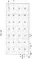
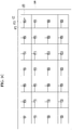
- FIGS. 1A , 1B , and 1C are top views of a display apparatus according to an exemplary embodiment.
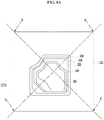
- FIG. 2A is a top view of a light emitting device according to an exemplary embodiment
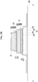
- FIG. 2B is a cross-sectional view taken along line A-A' of FIG. 2A
- FIG. 2C is a cross-sectional view taken along line B-B' of FIG. 2A .
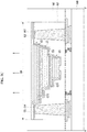
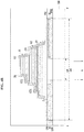
- FIGS. 3A and 3B are cross-sectional views of a light emitting device according to another exemplary embodiment.
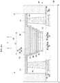
- FIGS. 4A and 4B are cross-sectional views of a light emitting device according to another exemplary embodiment.
- a display apparatus may include a substrate SUB and a plurality of light emitting devices LED disposed on the substrate SUB.
- FIGS. 1A and 1B are planar views of the display apparatus from a first surface of each of the plurality of light emitting devices LED.
- FIG. 1C is a planar view of the display apparatus from a second surface of each of the plurality of light emitting devices LED opposing the first surface.
- the substrate SUB may include a plastic substrate, which has flexibility and a visible light transmitting property.
- the plastic substrate may include at least one of a polyester resin, such as polyethylene terephthalate (PET) or polyethylene naphthalate (PEN), polyacrylonitrile resin, polyimide resin, polymethyl methacrylate resin, polycarbonate (PC) resin, polyethersulfone (PES) resin, polyamide resin, cycloolefin resin, polystyrene resin, polyamide imide resin, polyether imide resin, polydimethyl siloxane (PDMS) resin, polyetheretherketone (PEEK) resin, and polyvinylchloride resin.
- a polyester resin such as polyethylene terephthalate (PET) or polyethylene naphthalate (PEN)
- PET polyethylene naphthalate
- PES polyethersulfone
- PA polyamide resin
- cycloolefin resin polystyrene resin
- polyamide imide resin polyether
- the substrate SUB may be rolled in a first direction DR1.
- the plurality of light emitting devices LED may be disposed while being spaced apart from one another by a first distance DT1 in the first direction DR1, and by a second distance DT2 in a second direction DR2 perpendicular to the first direction DR1.
- the first distance DT1 may be greater than the second distance DT2.
- the substrate SUB may be easily rolled in the first direction DR1.
- the first distance DT1 may be substantially the same as the second distance DT2.
- Each of the first distance DT1 and the second distance DT2 between the light emitting devices LED may be about 8 to about 15 times the critical dimension (CD) of each light emitting device LED.
- the critical dimension (CD) of each light emitting device LED may be about 50 ⁇ m to about 80 ⁇ m.
- the substrate SUB may have a first hardness
- each of the light emitting devices LED may have a second hardness.
- the first hardness may be less than the second hardness. Since the light emitting devices LED, which have the small critical dimension of about 50 ⁇ m to about 80 ⁇ m, are sufficiently separated from each other by the first distance DT1 and the second distance DT2, even when the light emitting devices LED have a hardness greater than that of the substrate SUB, it is possible to prevent the light emitting devices LED from being damaged, such as being broken, when the substrate SUB is rolled or bent.
- the display apparatus may further include a protection layer PRT, which substantially fills between the light emitting devices LED and covers the light emitting devices LED on the substrate SUB.
- the protection layer PRT may include a material, which transmits visible light and is flexible.
- the protection layer PRT may include a silicon-based resin.
- the protection layer PRT may include a silicon-based resin, such as a siloxane-based resin or an epoxy resin.
- the protection layer PRT may include PDMS.
- a light emitting area LEA of each of the light emitting devices LED may be substantially the same as a light extraction area LEX.
- the light emitting area LEA may refer to an area, where each light emitting device LED emits light
- the light extraction area LEX may refer to an area, where light emitted in the light emitting area LEA is extracted to the outside.
- the light emitting area LEA and the light extraction area LEX may be defined based on one surface of the substrate SUB. For example, when the first distance DT1 and the second distance DT2 between the light emitting devices LED are the same, the distances between light extraction areas LEX may be the same. As another example, when the first distance DT1 between the light emitting devices LED is greater than the second distance DT2, the distances between light extraction areas LEX may be different from each other depending on the distance between the light emitting devices LED.
- the display apparatus may further include a light shielding layer LS, which substantially fills between the light emitting devices LED and partially covers the light emitting devices LED on the substrate SUB.
- the light shielding layer LS may include a material that has an insulating property and absorbs or shields light.
- the light shielding layer LS may include a photoresist or a black matrix. Portions of the light emitting devices LED where the light shielding layer LS is not formed may be protected by the protection layer PRT.
- the light extraction area LEX of each of the light emitting devices LED may be smaller than the light emitting area LEA. In this manner, it is possible to increase the contrast of light generated from each of the light emitting devices LED.
- a length of each light emitting device LED along the second direction DR2 may be greater than a length of each light emitting device LED, which is exposed by the light shielding layer LS (e.g., light extraction area LEX), along the second direction DR2. More particularly, the light shielding layer LS may partially cover each light emitting device LED along the second direction DR2, and thus, a length of the exposed light emitting device LED along the second direction may be less than a length of the light emitting device LED by the difference between the first distance DT1 and the second distance DT2.
- the light extraction areas LEX may be separated from one another by the same distance as the first distance DT1. In this manner, as the light extraction areas LEX are separated from one another by the same distance, the display apparatus including the light emitting devices LED may generate light uniformly throughout.
- each of the light emitting devices LED may include a first light emitting part LE1, a second light emitting part LE2, and a third light emitting part LE3, which are vertically stacked.
- the first light emitting part LE1 may generate light having the shortest wavelength
- the second light emitting part LE2 may generate light having a wavelength longer than the wavelength of light generated in the first light emitting part LE1 and shorter than the wavelength of light generated in the third light emitting part LE3
- the third light emitting part LE3 may generate light having the longest wavelength.
- the first light emitting part LE1 may emit blue light
- the second light emitting part LE2 may emit green light
- the third light emitting part LE3 may emit red light
- the color of light emitted from each of the first to third light emitting parts LE1, LE2, and LE3 is not limited thereto, and the colors may be variously changed.
- the first to third light emitting parts LE1, LE2, and LE3 may emit red light, blue light, and green light, respectively.
- each of the first to third light emitting parts LE1, LE2, and LE3 may emit light different from each other, or at least some of the light emitting parts may emit the same color light.
- the first light emitting part LE1 may include a first n-type semiconductor layer 102, a first active layer 104, a first p-type semiconductor layer 106, and a first ohmic layer 108.
- the second light emitting part LE2 may include a second n-type semiconductor layer 202, a second active layer 204, a second p-type semiconductor layer 206, and a second ohmic layer 208.
- the third light emitting part LE3 may include a third n-type semiconductor layer 302, a third active layer 304, a third p-type semiconductor layer 306, and a third ohmic layer 308.
- Each of the first n-type semiconductor layer 102, the second n-type semiconductor layer 202, and the third n-type semiconductor layer 302 may be a Si-doped gallium nitride-based semiconductor layer.
- Each of the first p-type semiconductor layer 106, the second p-type semiconductor layer 206, and the third p-type semiconductor layer 306 may be a Mg-doped gallium nitride-based semiconductor layer.
- Each of the first active layer 104, the second active layer 204, and the third active layer 304 may include a multi-quantum well (MQW), and the composition ratio thereof may be determined to emit light of a desired peak wavelength.
- MQW multi-quantum well
- TCO transparent conductive oxide
- ITO indium tin oxide
- ZITO zinc-doped indium tin oxide
- ZIO zinc indium oxide
- GIO gallium indium oxide
- ZTO zinc tin oxide
- FTO fluorine-doped t
- the first n-type semiconductor layer 102, the first active layer 104, the first p-type semiconductor layer 106, and the first ohmic layer 108 may be sequentially stacked in the first light emitting part LE1, the second ohmic layer 208, the second p-type semiconductor layer 206, the second active layer 204, and the second n-type semiconductor layer 202 may be sequentially stacked in the second light emitting part LE2, and the third ohmic layer 308, the third p-type semiconductor layer 306, the third active layer 304, and the third n-type semiconductor layer 302 may be sequentially stacked in the third light emitting part LE3.
- the second light emitting part LE2 may have a planar area smaller than that of the first light emitting part LE1
- the third light emitting part LE3 may have a planar area smaller than that of the second light emitting part LE2.
- the first light emitting part LE1 may have a structure, in which the first active layer 104, the first p-type semiconductor layer 106, and the first ohmic layer 108 are etched to expose a portion of the first n-type semiconductor layer 102.
- the second light emitting part LE2 may have a planar area smaller than that of the first light emitting part LE1 to expose the first ohmic layer 108, and may have a structure, in which the second p-type semiconductor layer 206, the second active layer 204, and the second n-type semiconductor layer 202 are etched to expose a portion of the second ohmic layer 208.
- the third light emitting part LE3 may have a planar area smaller than that of the second light emitting part LE2 to expose the second n-type semiconductor layer 202, and may have a structure, in which the third p-type semiconductor layer 306, the third active layer 304, and the third n-type semiconductor layer 302 are etched to expose a portion of the third ohmic layer 308.
- Each light emitting device LED may further include a first pad PD1 electrically coupled with the first n-type semiconductor layer 102, a second pad PD2 electrically coupled with the second n-type semiconductor layer 202, a third pad PD3 electrically coupled with the third n-type semiconductor layer 302, and a common pad CPD electrically coupled in common with the first ohmic layer 108, the second ohmic layer 208, and the third ohmic layer 308.
- Each of the first pad PD1, the second pad PD2, the third pad PD3, and the common pad CPD may include at least one of Au, Ag, Ni, Al, Rh, Pd, Ir, Ru, Mg, Zn, Pt, Hf, Cr, Ti, and Cu, or an alloy thereof.
- first ohmic layer 108, the second ohmic layer 208, and the third ohmic layer 308 are illustrated as being electrically coupled to the common pad CPD, however, the inventive concepts are not limited thereto.
- the first n-type semiconductor layer 102, the second n-type semiconductor layer 202, and the third n-type semiconductor layer 302 may be electrically coupled to the common pad CPD.
- the light emitting device LED may further include a first adhesion part AD1 disposed between the first light emitting part LE1 and the second light emitting part LE2 to bond the first light emitting part LE1 and the second light emitting part LE2, and a second adhesion part AD2 disposed between the second light emitting part LE2 and the third light emitting part LE3 to bond the second light emitting part LE2 and the third light emitting part LE3.
- Each of the first adhesion part AD1 and the second adhesion part AD2 may include a material, which has an insulating property, transmits visible light, and has a bonding characteristic.
- Each of the first adhesion part AD1 and the second adhesion part AD2 may include glass, a polymer, a resist, a polyimide, etc.
- each of the first adhesion part AD1 and the second adhesion part AD2 may include at least one of spin-on-glass (SOG), benzo cyclo butadiene (BCB), hydrogen silsesquioxanes (HSQ), and an SU-8 photoresist.
- SOG spin-on-glass
- BCB benzo cyclo butadiene
- HSQ hydrogen silsesquioxanes
- SU-8 photoresist an SU-8 photoresist
- the light emitting device LED may further include a first color filter CF1 disposed between the first light emitting part LE1 and the second light emitting part LE2, and a second color filter CF2 disposed between the second light emitting part LE2 and the third light emitting part LE3.
- the first color filter CF1 may reflect light emitted from the first light emitting part LE1 and pass light emitted from the second light emitting part LE2 and the third light emitting part LE3, so that light emitted from the first light emitting part LE1 does not exert an influence on each of the second light emitting part LE2 and the third light emitting part LE3.
- the second color filter CF2 may reflect light generated from each of the first light emitting part LE1 and the second light emitting part LE2 and pass light generated from the third light emitting part LE3, so that light generated from the first light emitting part LE1 and the second light emitting part LE2 does not exert an influence on the third light emitting part LE3.
- Each of the first color filter CF1 and the second color filter CF2 may include a distributed Bragg reflector (DBR), in which TiO 2 and SiO 2 are alternately stacked.
- DBR distributed Bragg reflector
- the alternation sequence or number of TiO 2 and SiO 2 in the second color filter CF2 may be different from the alternation sequence or number of TiO 2 and SiO 2 in the first color filter CF1.
- the light emitting device LED may further include a first contact pattern CT1, which is brought into electrical contact with the first n-type semiconductor layer 102, a first extended pattern EL1, which is brought into electrical contact with the first contact pattern CT1 and extends over the flat top surface of the first n-type semiconductor layer 102, and a first through pattern VA1, which electrically couples the first extended pattern EL1 and the first pad PD1.
- a first contact pattern CT1 which is brought into electrical contact with the first n-type semiconductor layer 102
- a first extended pattern EL1 which is brought into electrical contact with the first contact pattern CT1 and extends over the flat top surface of the first n-type semiconductor layer 102
- a first through pattern VA1 which electrically couples the first extended pattern EL1 and the first pad PD1.
- the light emitting device LED may further include a second contact pattern CT2, which is brought into electrical contact with the second n-type semiconductor layer 202, a second extended pattern EL2, which is brought into electrical contact with the second contact pattern CT2 and extends over the flat top surface of the first n-type semiconductor layer 102, and a second through pattern VA2, which electrically couples the second extended pattern EL2 and the second pad PD2.
- a second contact pattern CT2 which is brought into electrical contact with the second n-type semiconductor layer 202
- a second extended pattern EL2 which is brought into electrical contact with the second contact pattern CT2 and extends over the flat top surface of the first n-type semiconductor layer 102
- a second through pattern VA2 which electrically couples the second extended pattern EL2 and the second pad PD2.
- the light emitting device LED may further include a third contact pattern CT3, which is brought into electrical contact with the third n-type semiconductor layer 302, a third extended pattern EL3, which is brought into electrical contact with the third contact pattern CT3 and extends over the flat top surface of the first n-type semiconductor layer 102, and a third through pattern VA3, which electrically couples the third extended pattern EL3 and the third pad PD3.
- a third contact pattern CT3 which is brought into electrical contact with the third n-type semiconductor layer 302
- a third extended pattern EL3 which is brought into electrical contact with the third contact pattern CT3 and extends over the flat top surface of the first n-type semiconductor layer 102
- a third through pattern VA3 which electrically couples the third extended pattern EL3 and the third pad PD3.
- the light emitting device LED may further include a first common contact pattern CCT1, which is brought into electrical contact with the first ohmic layer 108 and the second ohmic layer 208, a second common contact pattern CCT2, which is brought into electrical contact with the third ohmic layer 308, a common extended pattern CEL, which is brought into electrical contact with the first common contact pattern CCT1 and the second common contact patter CCT2 and extends over the flat top surface of the first n-type semiconductor layer 102, and a common through pattern CVA, which electrically couples the common extended pattern CEL and the common pad CPD.
- each of the first pad PD1, the second pad PD2, the third pad PD3, and the common pad CPD may be disposed between the third light emitting part LE3 and the substrate SUB.
- the first through pattern VA1, the second through pattern VA2, the third through pattern VA3, and the common through pattern CVA may have substantially the same height as each being disposed on the first extended pattern EL1, the second extended pattern EL2, the third extended pattern EL3, and the common extended pattern CEL, respectively, which extend over the flat top surface of the first n-type semiconductor layer 102.
- each of the first pad PD1, the second pad PD2, the third pad PD3, and the common pad CPD may extend onto a passivation layer PVT, which covers the light emitting device LED.
- the first pad PD1, the second pad PD2, the third pad PD3, and the common pad CPD may be easily mounted to the substrate SUB as each of the first pad PD1, the second pad PD2, the third pad PD3, and the common pad CPD extend on the passivation layer PVT.
- each third light emitting part LE3 may be disposed to face the substrate SUB, and one surface of each first light emitting part LE1 may include the light emitting area LEA.
- the light emitting devices LED may be isolated from one another by the protection layer PRT.
- the display apparatus may further include the light shielding layer LS, which substantially fills between the light emitting devices LED and partially covers one surface of the first light emitting parts LE1 of the light emitting devices LED.
- the width of the first n-type semiconductor layer 102 of each first light emitting part LE1 may define the light emitting area LEA.
- the light shielding layer LS may partially cover the light emitting area LEA, and may define the light extraction area LEX. In this case, the light extraction area LEX may be smaller than the light emitting area LEA.
- the light shielding layer LS partially covers the first surface of each of the light emitting devices LED, the area of the first surface through which light is extracted is reduced, and thus, it is possible to increase the contrast of light generated from each of the light emitting devices LED.
- the light emitting device LED may further include a first contact pattern CT1, which is brought into electrical contact with the first n-type semiconductor layer 102, and a first extended pattern EL1, which is brought into electrical contact with the first contact pattern CT1 and extends from the third light emitting part LE3 of the light emitting device LED to the first light emitting part LE1.
- the light emitting device LED may further include a second contact pattern CT2, which is brought into electrical contact with the second n-type semiconductor layer 202, and a second extended pattern EL2, which is brought into electrical contact with the second contact pattern CT2 and extends from the third light emitting part LE3 of the light emitting device LED to the first light emitting part LE1.
- the light emitting device LED may further include a third contact pattern CT3, which is brought into electrical contact with the third n-type semiconductor layer 302, and a third extended pattern EL3, which is brought into electrical contact with the third contact pattern CT3 and extends from the third light emitting part LE3 of the light emitting device LED to the first light emitting part LE1.
- the light emitting device LED may further include a first common contact pattern CCT1, which is brought into electrical contact with the first ohmic layer 108 and the second ohmic layer 208, a second common contact pattern CCT2, which is brought into electrical contact with the third ohmic layer 308, and a common extended pattern CEL, which is brought into electrical contact with the first common contact pattern CCT1 and the second common contact patter CCT2 and extends from the third light emitting part LE3 of the light emitting device LED to the first light emitting part LE1.
- the first light emitting part LE1 may face the substrate SUB, and one surface of the substrate SUB facing away the first light emitting parts LE1 may include a light extraction surface.
- Each of the first extended pattern EL1, the second extended pattern EL2, the third extended pattern EL3, and the common extended pattern CEL illustrated in FIGS. 4A and 4B may include at least one of Au, Ag, Ni, Al, Rh, Pd, Ir, Ru, Mg, Zn, Pt, Hf, Cr, Ti, and Cu, or an alloy thereof.
- As the first extended pattern EL1, the second extended pattern EL2, the third extended pattern EL3, and the common extended pattern CEL including metal are disposed on the side surface of the light emitting device LED by extending from the third light emitting part LE3 of the light emitting device LED to the first light emitting part LE1, they may also function as a light shielding layer. Also, a width may gradually decrease from the first light emitting part LE1 toward the third light emitting part LE3. As such, it is possible to easily roll or bend the substrate SUB, on which the plurality of light emitting devices LED are disposed.
- the display apparatus may further include first substrate pads SPD1, second substrate pads SPD2, third substrate pads SPD3, and common substrate pads SCPD, which are electrically coupled with first pads PD1, second pads PD2, third pads PD3 and common pads CPD, respectively.
- the first substrate pads SPD1, the second substrate pads SPD2, the third substrate pads SPD3, and the common substrate pads SCPD may be disposed at positions corresponding to the first pads PD1, the second pads PD2, the third pads PD3, and the common pads CPD, and may be electrically bonded thereto by a conductive material, such as solder balls SD.
- the display apparatus may further include a common circuit CC (see FIG. 1C ), which is electrically coupled with the common substrate pads SCPD on one surface of the substrate SUB facing the light emitting devices LED.
- the common circuit CC may have a mesh structure, and electrically couple the plurality of common substrate pads SCPD.
- the common substrate pads SCPD of the light emitting devices LED may be electrically coupled with one another by the common circuit CC.
- the common circuit CC may include first extensions ET1 and second extensions ET2, which are electrically coupled with the common substrate pads SCPD.
- the common circuit CC which applies a predetermined voltage to the common substrate pads SCPD, electrically couples the common pads CPD of the plurality of light emitting devices LED by the mesh structure, even when the common circuit CC or some of the common substrate pads SCPD are damaged while the substrate SUB is rolled, the predetermined voltage may be applied to the common pads CPD.
- Each light emitting device of a display apparatus may be changed variously, which will be described in more detail below.
- FIG. 5A is a top view of a light emitting device according to another exemplary embodiment
- FIG. 5B is a cross-sectional view taken along line A-A' of FIG. 5A .
- a light emitting device may include a first light emitting part LE1, a second light emitting part LE2, and a third light emitting part LE3, which are horizontally spaced apart from one another on the same plane.
- the first light emitting part LE1 may include a first n-type semiconductor layer 102, a first active layer 104, a first p-type semiconductor layer 106, and a first ohmic layer 108.
- the first active layer 104, the first p-type semiconductor layer 106, and the first ohmic layer 108 may have a mesa structure, such that a portion of the first n-type semiconductor layer 102 is exposed.
- the second light emitting part LE2 may include a second n-type semiconductor layer 202, a second active layer 204, a second p-type semiconductor layer 206, and a second ohmic layer 208.
- the second active layer 204, the second p-type semiconductor layer 206, and the second ohmic layer 208 may have a mesa structure, such that a portion of the second n-type semiconductor layer 202 is exposed.
- the third light emitting part LE3 may include a third n-type semiconductor layer 302, a third active layer 304, a third p-type semiconductor layer 306, and a third ohmic layer 308.
- the third active layer 304, the third p-type semiconductor layer 306, and the third ohmic layer 308 may have a mesa structure, such that a portion of the third n-type semiconductor layer 302 is exposed.
- a first pad PD1 may be electrically coupled with the first ohmic layer 108 through a first contact pattern CT1
- a second pad PD2 may be electrically coupled with the second ohmic layer 208 through a second contact pattern CT2
- a third pad PD3 may be electrically coupled with the third ohmic layer 308 through a third contact pattern CT3.
- the first n-type semiconductor layer 102, the second n-type semiconductor layer 202, and the third n-type semiconductor layer 302 may be electrically coupled by a common pad CPD, which couples a first common contact pattern CCT1, a second common contact pattern CCT2, and a third common contact pattern.
- first n-type semiconductor layer 102, the second n-type semiconductor layer 202, and the third n-type semiconductor layer 302 are illustrated as being electrically coupled to the common pad CPD, however, the inventive concepts are not limited thereto.
- the first ohmic layer 108, the second ohmic layer 208, and the third ohmic layer 308 may be electrically coupled to the common pad CPD.
- FIGS. 5A and 5B Elements of the light emitting device shown in FIGS. 5A and 5B are substantially the same as those of the light emitting device show in FIGS. 1A , 1B , 2a , 2B , 2C , 3A , 3B , 4A , and 4B , and thus, repeated descriptions of the substantially the same elements will be omitted to avoid redundancy.
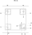
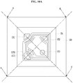
- FIG. 6A is a top view of a light emitting device according to another exemplary embodiment
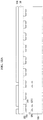
- FIG. 6B is a cross-sectional view taken along lines A-A' and B-B' of FIG. 6A .
- a light emitting device may include a first light emitting part LE1, a second light emitting part LE2, and a third light emitting part LE3, which are vertically stacked.
- the first light emitting part LE1 may include a first n-type semiconductor layer 102, a first active layer 104, a first p-type semiconductor layer 106, and a first ohmic layer 108, which are vertically stacked.
- the second light emitting part LE2 may include a second n-type semiconductor layer 202, a second active layer 204, a second p-type semiconductor layer 206, and a second ohmic layer 208, which are vertically stacked.
- the third light emitting part LE3 may include a third ohmic layer 308, a third p-type semiconductor layer 306, a third active layer 304, and a third n-type semiconductor layer 302, which are vertically stacked.
- a first pad PD1 may be electrically coupled with the first n-type semiconductor layer 102 through a first through pattern VA1, which passes through the first light emitting part LE1, the second light emitting part LE2, and the third light emitting part LE3.
- a second pad PD2 may be electrically coupled with the second n-type semiconductor layer 202 through a second through pattern VA2, which passes through the second light emitting part LE2 and the third light emitting part LE3.
- a third pad PD3 may be electrically coupled with the third n-type semiconductor layer 302 through a third through pattern VA3.
- a common pad CPD may be electrically coupled with the first ohmic layer 108, the second ohmic layer 208, and the third ohmic layer 308 through a fourth through pattern VA4, which is electrically coupled with the first ohmic layer 108 by passing through the second light emitting part LE2 and the third light emitting part LE3, a fifth through pattern VA5, which is electrically coupled with the second ohmic layer 208 by passing through the third light emitting part LE3, and a sixth through pattern VA6, which is electrically coupled with the third ohmic layer 308.
- the light emitting device may further include a first adhesion part AD1, a second adhesion part AD2, a first color filter CF1, and a second color filter CF2.
- FIGS. 6A and 6b Elements of the light emitting device shown in FIGS. 6A and 6b are substantially the same as those of the light emitting device shown in FIGS. 1A , 1B , 2A , 2B , 2C , 3A , 3B , 4A , and 4B , and thus, repeated descriptions of the substantially the same elements will be omitted to avoid redundancy.
- FIGS. 1A , 2A , 2B , and 2C a method for manufacturing the light emitting device shown in FIGS. 1A , 2A , 2B , and 2C will be exemplarily described.
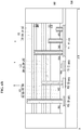
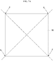
- FIGS. 7A to 12A are top views illustrating a method for manufacturing a light emitting device according to an exemplary embodiment
- FIGS. 7B to 12B are cross-sectional views taken along the lines A-A' of FIGS. 7A to 12A
- FIGS. 7C to 12C are cross-sectional views taken along the lines B-B' of FIGS. 7A to 12A , respectively.
- a first light emitting part LE1 may be formed.
- a first color filter CF1 may be additionally formed on the first ohmic layer 108. However, in some exemplary embodiments, the first color filter CF1 may be omitted.
- a second light emitting part LE2 may be formed.
- a third n-type semiconductor layer 302 a third active layer 304, a third p-type semiconductor layer 306, and a third ohmic layer 308 on a third substrate.
- a second color filter CF2 may be additionally formed on the third ohmic layer 308. However, in some exemplary embodiments, the second color filter CF2 may be omitted.
- the second substrate may be removed by using laser lift-off (LLO) or chemical lift-off (CLO).
- LLO laser lift-off
- CLO chemical lift-off
- the third substrate may be removed by using LLO or CLO.
- the third ohmic layer 308 may be exposed by etching the third n-type semiconductor layer 302, the third active layer 304, and the third p-type semiconductor layer 306 through using a first mask
- the second n-type semiconductor layer 202 may be exposed by etching the third ohmic layer 308 and the first adhesion part AD1 through using a second mask
- the second ohmic layer 208 may be exposed by etching the second n-type semiconductor layer 202, the second active layer 204, and the second p-type semiconductor layer 206 through using a third mask
- the first ohmic layer 108 may be exposed by etching the second ohmic layer 208 and the first adhesion part AD1 through using a fourth mask
- the first n-type semiconductor layer 102 may be exposed by etching the first ohmic layer 108, the first p-type semiconductor layer 106, and the first active layer 104 through using a
- a dielectric layer IDL covering the etched structure may be formed.
- the dielectric layer IDL may include one of SiO x , SiN x , Al x O y , and SiO x N y .
- openings that expose the first n-type semiconductor layer 102, the second n-type semiconductor layer 202, the third n-type semiconductor layer 302, the first ohmic layer 108, the second ohmic layer 208, and the third ohmic layer 308 may be formed.
- a first contact pattern CT1 that is brought into electrical contact with the first n-type semiconductor layer 102 exposed by the opening of the dielectric layer IDL, a second contact pattern CT2 that is brought into electrical contact with the second n-type semiconductor layer 202 exposed by the opening of the dielectric layer IDL, a third contact pattern CT3 that is brought into electrical contact with the third n-type semiconductor layer 302 exposed by the opening of the dielectric layer IDL, a first common contact pattern CCT1 that is brought into electrical contact with the first ohmic layer 108 and the second ohmic layer 208 exposed by the openings of the dielectric layer IDL, and a second common contact pattern CCT2 that is brought into electrical contact with the third ohmic layer 308 exposed by the opening of the dielectric layer IDL may be formed.
- a first extended pattern EL1 that is brought into electrical contact with the first contact pattern CT1 and extending along the side surfaces of the first light emitting part LE1, the second light emitting part LE2, and the third light emitting part LE3 and onto the dielectric layer IDL formed on the substantially flat surface of the first n-type semiconductor layer 102
- a second extended pattern EL2 that is brought into electrical contact with the second contact pattern CT2 and extending along the side surfaces of the first light emitting part LE1, the second light emitting part LE2, and the third light emitting part LE3 and onto the dielectric layer IDL formed on the substantially flat surface of the first n-type semiconductor layer 102
- a third extended pattern EL3 that is brought into electrical contact with the third contact pattern CT3 and extending along the side surfaces of the first light emitting part LE1, the second light emitting part LE2, and the third light emitting part LE3 and onto the dielectric layer IDL formed on the substantially flat surface of the first n-type semiconductor layer 102
- a passivation layer PVT which covers the first light emitting part LE1, the second light emitting part LE2, the third light emitting part LE3, the first extended pattern EL1, the second extended pattern EL2, the third extended pattern EL3, and the common extended pattern CEL may be formed.
- the passivation layer PVT may include at least one inorganic material or at least one organic material.
- the organic materials may include acryl, glass, polymer, resist, polyimide, polyamide, spin on glass (SOG), benzocyclobutene (BCG), benzocyclobutene (BCB), hydrogen silsesquioxane (HSQ), or SU-8 photoresist and the like, and the inorganic materials may include one of SiO x , SiN x , Al x O y , and SiO x N y .
- the passivation film PVT may be formed transparent without color, or may have various colors.
- the passivation layer PVT may be provided transparently or may be formed as black or white.
- a first through pattern VA1, a second through pattern VA2, a third through pattern VA3, and a common through pattern CVA may be respectively formed.
- a first pad PD1 electrically coupled with the first through pattern VA1, a second pad PD2 electrically coupled with the second through pattern VA2, a third pad PD3 electrically coupled with the third through pattern VA3, and a common pad CPD electrically coupled with the common through pattern CVA may be respectively formed.
- a plurality of light emitting devices may be formed on the first substrate SUB.
- FIGS. 13A and 13B are cross-sectional illustrating a method for mounting light emitting devices to a mounting substrate according to an exemplary embodiment.
- a first substrate 100 on which the light emitting devices LED are formed, may be turned over to face a target mounting substrate SUB. After forming a mask pattern MSK on one surface of the first substrate 100, light emitting device LED may be selectively separated from the substrate 100 in consideration of a separation distance, by performing selective laser lift-off (LLO) on the first substrate 100.
- LLO laser lift-off
- a first substrate pad SPD1, a second substrate pad SPD2, a third substrate pad SPD3, and a common substrate pad SCPD may be respectively formed.
- the light emitting devices LED may be mounted to the substrate SUB.
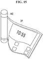
- FIGS. 14 and 15 are diagrams exemplarily illustrating electronic apparatuses, to which the display apparatus according to exemplary embodiments may be applied.
- an electronic apparatus may be a wristwatch.
- the electronic apparatus may include a housing HS, which surrounds the wrist, and a display part DP, which may be rolled to be moved into and out of the housing HS.
- the display part DP may include the display apparatus described above with reference to FIGS. 1A , 1B , 2A , 2B , 2C , 3A , 3B , 4A , and 4B .
- the area of the display part DP may be adjusted.
- the plurality of light emitting devices of the display part DP may be electrically coupled with individual driving circuits.
- an electronic apparatus may be a rollable screen.
- the electronic apparatus may include a housing HS and a display part DP, which may be rolled to be moved into and out of the housing HS.
- the display part DP may include the display apparatus described above with reference to FIGS. 1A to 4B .
- the wristwatch and the rollable screen are exemplarily described as the electronic apparatuses in the illustrated exemplary embodiments, however, the inventive concepts are not limited thereto.
- the display apparatus according to exemplary embodiments may be applied to various electronic apparatuses.
Landscapes
- Physics & Mathematics (AREA)
- General Physics & Mathematics (AREA)
- Engineering & Computer Science (AREA)
- Theoretical Computer Science (AREA)
- Led Device Packages (AREA)
- Devices For Indicating Variable Information By Combining Individual Elements (AREA)
- Led Devices (AREA)
Abstract


Description
- Exemplary embodiments of the invention relate generally to a display apparatus and, more specifically, to a flexible display apparatus.
- In general, a display apparatus includes a display panel, which displays an image by using light, and a backlight unit, which provides light to the display panel. The display panel includes a plurality of pixel cells each including a switching element, a pixel electrode, a common electrode, and a color layer. As the display panel, a liquid crystal display panel is widely used. Light provided by the backlight unit passes through liquid crystals and the color layer, and the display apparatus may display a color image by mixture of colored lights. The color layer for displaying a color image includes, for example, a red color filter, a green color filter, and a blue color filter. By mixing of light having passed through the color filters, various colors may be displayed. As such, in order to realize light of various colors for displaying an image, the color filters are needed.
- Moreover, liquid crystals may require polarization, and thus, a polarizing filter and various optical films are typically needed. As such, the display apparatus becomes thick and heavy.
- A display apparatus including a plurality of light emitting diodes constructed according to exemplary embodiments of the invention are capable of obviating the need of at least one or more components of a conventional display apparatus, such as liquid crystals, a backlight unit, a polarizing filter and, a color filter.
- Additional features of the inventive concepts will be set forth in the description which follows, and in part will be apparent from the description, or may be learned by practice of the inventive concepts.
- A display apparatus according to an exemplary embodiment includes a flexible substrate, a plurality of light emitting devices spaced apart from one another and disposed on the flexible substrate, and a light shielding layer disposed between the light emitting devices, and partially covering the light emitting devices to define light extraction surfaces, in which a distance between adjacent light extraction areas is the same.
- The light emitting devices may be spaced apart from one another by a first distance in a first direction, and by a second distance in a second direction perpendicular to the first direction, and the first distance may be equal to or greater than the second distance.
- The substrate may be configured to be rolled in the first direction.
- The first distance may be greater than the second distance, and a length of each light emitting device in the second direction may be greater than a length of a corresponding light extraction area in the second direction.
- The display apparatus may further include a common circuit electrically coupled in common with the light emitting devices, in which the common circuit may be disposed on the substrate and have a mesh structure.
- The display apparatus may further include a protection layer covering the light emitting devices on the substrate, the protection layer including a material that transmits visible light.
- A hardness of the substrate may be less than a hardness of each of the light emitting devices.
- Each of the light emitting devices may include a first light emitting part, a second light emitting part, and a third light emitting part horizontally spaced apart from one another on the substrate.
- Each of the light emitting devices may include a first light emitting part, a second light emitting part, and a third light emitting part, which are vertically stacked on the substrate.
- The third light emitting part may have a width less than that of the second light emitting part, and the second light emitting part has a width less than that of the first light emitting part.
- Each of the light emitting devices may have a width that gradually decreases in an upward direction from one surface of the substrate.
- The details of other embodiments are included in the detailed description and the drawings.
- In the display apparatus in accordance with the embodiments of the disclosure, by displaying a plurality of light emitting devices each including a plurality of light emitting parts, on a flexible substrate, it is possible to extract light of high efficiency with small power consumption, whereby the display apparatus may be applied to various electronic apparatuses.
-
-
FIGS. 1A ,1B , and1C are top views of a display apparatus according to an exemplary embodiment. -
FIG. 2A is a top view of a light emitting device according to an exemplary embodiment. -
FIG. 2B is a cross-sectional view taken along line A-A' ofFIG. 2A . -
FIG. 2C is a cross-sectional view taken along line B-B' ofFIG. 2A . -
FIGS. 3A and3B are cross-sectional views of a light emitting device according to another exemplary embodiment. -
FIGS. 4A and4B are cross-sectional views of a light emitting device according to another exemplary embodiment. -
FIG. 5A is a top view of a light emitting device according to another exemplary embodiment. -
FIG. 5B is a cross-sectional view taken along line A-A' ofFIG. 5A . -
FIG. 6A is a top view of a light emitting device according to another exemplary embodiment. -
FIG. 6B is a cross-sectional view taken along lines A-A' and B-B' of the light emitting device ofFIG. 6A . -
FIGS. 7A ,8A ,9A ,10A ,11A , and12A are top views illustrating a method for manufacturing a light emitting device according to an exemplary embodiment. -
FIGS. 7B ,8B ,9B ,10B ,11B , and12B are cross-sectional views taken along lines A-A' ofFIGS. 7A ,8A ,9A ,10A ,11A , and12A , respectively. -
FIGS. 7C ,8C ,9C ,10C ,11C , and12C are cross-sectional views taken along lines B-B' ofFIGS. 7A ,8A ,9A ,10A ,11A , and12A , respectively. -
FIGS. 13A and13B are cross-sectional views illustrating a method for mounting light emitting devices to a mounting substrate according to an exemplary embodiment. -
FIGS. 14 and15 are diagrams illustrating electronic apparatuses to which the display apparatus according to an exemplary embodiment is applied. - In order to understand the configuration and effect of the disclosure sufficiently, embodiments of the disclosure will be described with reference to the accompanying drawings. However, the disclosure is not limited to the embodiments set forth herein and may be implemented in various forms, and a variety of changes may be added.
- Hereinafter, a display apparatus will be described below with reference to the accompanying drawings through various examples of embodiments.
- As used in the embodiments of the disclosure, a technical term may be interpreted as a meaning conventionally known to those of ordinary skill in the art unless defined otherwise.
-
FIGS. 1A ,1B , and1C are top views of a display apparatus according to an exemplary embodiment.FIG. 2A is a top view of a light emitting device according to an exemplary embodiment,FIG. 2B is a cross-sectional view taken along line A-A' ofFIG. 2A , andFIG. 2C is a cross-sectional view taken along line B-B' ofFIG. 2A .FIGS. 3A and3B are cross-sectional views of a light emitting device according to another exemplary embodiment.FIGS. 4A and4B are cross-sectional views of a light emitting device according to another exemplary embodiment. - Referring to
FIGS. 1A ,1B ,1C ,2A ,2B ,2C ,3A ,3B ,4A , and4B , a display apparatus may include a substrate SUB and a plurality of light emitting devices LED disposed on the substrate SUB.FIGS. 1A and1B are planar views of the display apparatus from a first surface of each of the plurality of light emitting devices LED.FIG. 1C is a planar view of the display apparatus from a second surface of each of the plurality of light emitting devices LED opposing the first surface. - The substrate SUB may include a plastic substrate, which has flexibility and a visible light transmitting property. The plastic substrate may include at least one of a polyester resin, such as polyethylene terephthalate (PET) or polyethylene naphthalate (PEN), polyacrylonitrile resin, polyimide resin, polymethyl methacrylate resin, polycarbonate (PC) resin, polyethersulfone (PES) resin, polyamide resin, cycloolefin resin, polystyrene resin, polyamide imide resin, polyether imide resin, polydimethyl siloxane (PDMS) resin, polyetheretherketone (PEEK) resin, and polyvinylchloride resin. However, the inventive concepts are not limited thereto.
- According to an exemplary embodiment, the substrate SUB may be rolled in a first direction DR1.
- On a first surface of the substrate SUB, the plurality of light emitting devices LED may be disposed while being spaced apart from one another by a first distance DT1 in the first direction DR1, and by a second distance DT2 in a second direction DR2 perpendicular to the first direction DR1. According to an exemplary embodiment, the first distance DT1 may be greater than the second distance DT2. In this case, as the light emitting devices LED are separated from one another by a greater distance in the first direction DR1 than in the second direction DR2, the substrate SUB may be easily rolled in the first direction DR1. According to another exemplary embodiment, the first distance DT1 may be substantially the same as the second distance DT2.
- Each of the first distance DT1 and the second distance DT2 between the light emitting devices LED may be about 8 to about 15 times the critical dimension (CD) of each light emitting device LED. According to an exemplary embodiment, the critical dimension (CD) of each light emitting device LED may be about 50 µm to about 80 µm.
- According to an exemplary embodiment, the substrate SUB may have a first hardness, and each of the light emitting devices LED may have a second hardness. The first hardness may be less than the second hardness. Since the light emitting devices LED, which have the small critical dimension of about 50 µm to about 80 µm, are sufficiently separated from each other by the first distance DT1 and the second distance DT2, even when the light emitting devices LED have a hardness greater than that of the substrate SUB, it is possible to prevent the light emitting devices LED from being damaged, such as being broken, when the substrate SUB is rolled or bent.
- Referring to
FIG. 1A , the display apparatus according to the illustrated exemplary embodiment may further include a protection layer PRT, which substantially fills between the light emitting devices LED and covers the light emitting devices LED on the substrate SUB. The protection layer PRT may include a material, which transmits visible light and is flexible. The protection layer PRT may include a silicon-based resin. In particular, the protection layer PRT may include a silicon-based resin, such as a siloxane-based resin or an epoxy resin. For example, the protection layer PRT may include PDMS. In this case, a light emitting area LEA of each of the light emitting devices LED may be substantially the same as a light extraction area LEX. The light emitting area LEA may refer to an area, where each light emitting device LED emits light, and the light extraction area LEX may refer to an area, where light emitted in the light emitting area LEA is extracted to the outside. The light emitting area LEA and the light extraction area LEX may be defined based on one surface of the substrate SUB. For example, when the first distance DT1 and the second distance DT2 between the light emitting devices LED are the same, the distances between light extraction areas LEX may be the same. As another example, when the first distance DT1 between the light emitting devices LED is greater than the second distance DT2, the distances between light extraction areas LEX may be different from each other depending on the distance between the light emitting devices LED. - Referring to
FIG. 1B , the display apparatus according to another exemplary embodiment may further include a light shielding layer LS, which substantially fills between the light emitting devices LED and partially covers the light emitting devices LED on the substrate SUB. The light shielding layer LS may include a material that has an insulating property and absorbs or shields light. For example, the light shielding layer LS may include a photoresist or a black matrix. Portions of the light emitting devices LED where the light shielding layer LS is not formed may be protected by the protection layer PRT. In this case, due to the light shielding layer LS, the light extraction area LEX of each of the light emitting devices LED may be smaller than the light emitting area LEA. In this manner, it is possible to increase the contrast of light generated from each of the light emitting devices LED. - In the light emitting devices LED of
FIG. 1B , when the first distance DT1 is greater than the second distance DT2, and the light shielding layer LS partially covers each light emitting device LED along the first direction DR1, a length of each light emitting device LED along the second direction DR2 may be greater than a length of each light emitting device LED, which is exposed by the light shielding layer LS (e.g., light extraction area LEX), along the second direction DR2. More particularly, the light shielding layer LS may partially cover each light emitting device LED along the second direction DR2, and thus, a length of the exposed light emitting device LED along the second direction may be less than a length of the light emitting device LED by the difference between the first distance DT1 and the second distance DT2. As such, the light extraction areas LEX may be separated from one another by the same distance as the first distance DT1. In this manner, as the light extraction areas LEX are separated from one another by the same distance, the display apparatus including the light emitting devices LED may generate light uniformly throughout. - Referring to
FIGS. 2A ,2B ,2C ,3A , and3B , each of the light emitting devices LED may include a first light emitting part LE1, a second light emitting part LE2, and a third light emitting part LE3, which are vertically stacked. According to an exemplary embodiment, the first light emitting part LE1 may generate light having the shortest wavelength, the second light emitting part LE2 may generate light having a wavelength longer than the wavelength of light generated in the first light emitting part LE1 and shorter than the wavelength of light generated in the third light emitting part LE3, and the third light emitting part LE3 may generate light having the longest wavelength. For example, the first light emitting part LE1 may emit blue light, the second light emitting part LE2 may emit green light, and the third light emitting part LE3 may emit red light. However, the color of light emitted from each of the first to third light emitting parts LE1, LE2, and LE3 is not limited thereto, and the colors may be variously changed. For example, the first to third light emitting parts LE1, LE2, and LE3 may emit red light, blue light, and green light, respectively. Alternatively, each of the first to third light emitting parts LE1, LE2, and LE3 may emit light different from each other, or at least some of the light emitting parts may emit the same color light. - The first light emitting part LE1 may include a first n-
type semiconductor layer 102, a firstactive layer 104, a first p-type semiconductor layer 106, and a firstohmic layer 108. The second light emitting part LE2 may include a second n-type semiconductor layer 202, a secondactive layer 204, a second p-type semiconductor layer 206, and a secondohmic layer 208. The third light emitting part LE3 may include a third n-type semiconductor layer 302, a thirdactive layer 304, a third p-type semiconductor layer 306, and a thirdohmic layer 308. - Each of the first n-
type semiconductor layer 102, the second n-type semiconductor layer 202, and the third n-type semiconductor layer 302 may be a Si-doped gallium nitride-based semiconductor layer. Each of the first p-type semiconductor layer 106, the second p-type semiconductor layer 206, and the third p-type semiconductor layer 306 may be a Mg-doped gallium nitride-based semiconductor layer. Each of the firstactive layer 104, the secondactive layer 204, and the thirdactive layer 304 may include a multi-quantum well (MQW), and the composition ratio thereof may be determined to emit light of a desired peak wavelength. As each of the firstohmic layer 108, the secondohmic layer 208, and the thirdohmic layer 308, at least one of a transparent conductive oxide (TCO), such as indium tin oxide (ITO), zinc-doped indium tin oxide (ZITO), zinc indium oxide (ZIO), gallium indium oxide (GIO), zinc tin oxide (ZTO), fluorine-doped tin oxide (FTO), aluminum-doped zinc oxide (AZO), gallium-doped zinc oxide (GZO), indium tin oxide (In4Sn3O12), and zinc magnesium oxide (Zn(1-x)MgxO, 0≤x≤1) may be used. The first n-type semiconductor layer 102, the firstactive layer 104, the first p-type semiconductor layer 106, and the firstohmic layer 108 may be sequentially stacked in the first light emitting part LE1, the secondohmic layer 208, the second p-type semiconductor layer 206, the secondactive layer 204, and the second n-type semiconductor layer 202 may be sequentially stacked in the second light emitting part LE2, and the thirdohmic layer 308, the third p-type semiconductor layer 306, the thirdactive layer 304, and the third n-type semiconductor layer 302 may be sequentially stacked in the third light emitting part LE3. According to an exemplary embodiment, the second light emitting part LE2 may have a planar area smaller than that of the first light emitting part LE1, and the third light emitting part LE3 may have a planar area smaller than that of the second light emitting part LE2. For example, the first light emitting part LE1 may have a structure, in which the firstactive layer 104, the first p-type semiconductor layer 106, and the firstohmic layer 108 are etched to expose a portion of the first n-type semiconductor layer 102. The second light emitting part LE2 may have a planar area smaller than that of the first light emitting part LE1 to expose the firstohmic layer 108, and may have a structure, in which the second p-type semiconductor layer 206, the secondactive layer 204, and the second n-type semiconductor layer 202 are etched to expose a portion of the secondohmic layer 208. The third light emitting part LE3 may have a planar area smaller than that of the second light emitting part LE2 to expose the second n-type semiconductor layer 202, and may have a structure, in which the third p-type semiconductor layer 306, the thirdactive layer 304, and the third n-type semiconductor layer 302 are etched to expose a portion of the thirdohmic layer 308. - Each light emitting device LED may further include a first pad PD1 electrically coupled with the first n-
type semiconductor layer 102, a second pad PD2 electrically coupled with the second n-type semiconductor layer 202, a third pad PD3 electrically coupled with the third n-type semiconductor layer 302, and a common pad CPD electrically coupled in common with the firstohmic layer 108, the secondohmic layer 208, and the thirdohmic layer 308. Each of the first pad PD1, the second pad PD2, the third pad PD3, and the common pad CPD may include at least one of Au, Ag, Ni, Al, Rh, Pd, Ir, Ru, Mg, Zn, Pt, Hf, Cr, Ti, and Cu, or an alloy thereof. - While the first
ohmic layer 108, the secondohmic layer 208, and the thirdohmic layer 308 are illustrated as being electrically coupled to the common pad CPD, however, the inventive concepts are not limited thereto. For example, in some exemplary embodiments, the first n-type semiconductor layer 102, the second n-type semiconductor layer 202, and the third n-type semiconductor layer 302 may be electrically coupled to the common pad CPD. - The light emitting device LED may further include a first adhesion part AD1 disposed between the first light emitting part LE1 and the second light emitting part LE2 to bond the first light emitting part LE1 and the second light emitting part LE2, and a second adhesion part AD2 disposed between the second light emitting part LE2 and the third light emitting part LE3 to bond the second light emitting part LE2 and the third light emitting part LE3. Each of the first adhesion part AD1 and the second adhesion part AD2 may include a material, which has an insulating property, transmits visible light, and has a bonding characteristic. Each of the first adhesion part AD1 and the second adhesion part AD2 may include glass, a polymer, a resist, a polyimide, etc. For example, each of the first adhesion part AD1 and the second adhesion part AD2 may include at least one of spin-on-glass (SOG), benzo cyclo butadiene (BCB), hydrogen silsesquioxanes (HSQ), and an SU-8 photoresist.
- In some exemplary embodiments, the light emitting device LED may further include a first color filter CF1 disposed between the first light emitting part LE1 and the second light emitting part LE2, and a second color filter CF2 disposed between the second light emitting part LE2 and the third light emitting part LE3. The first color filter CF1 may reflect light emitted from the first light emitting part LE1 and pass light emitted from the second light emitting part LE2 and the third light emitting part LE3, so that light emitted from the first light emitting part LE1 does not exert an influence on each of the second light emitting part LE2 and the third light emitting part LE3. The second color filter CF2 may reflect light generated from each of the first light emitting part LE1 and the second light emitting part LE2 and pass light generated from the third light emitting part LE3, so that light generated from the first light emitting part LE1 and the second light emitting part LE2 does not exert an influence on the third light emitting part LE3. Each of the first color filter CF1 and the second color filter CF2 may include a distributed Bragg reflector (DBR), in which TiO2 and SiO2 are alternately stacked. For example, the alternation sequence or number of TiO2 and SiO2 in the second color filter CF2 may be different from the alternation sequence or number of TiO2 and SiO2 in the first color filter CF1.
- The light emitting device LED may further include a first contact pattern CT1, which is brought into electrical contact with the first n-
type semiconductor layer 102, a first extended pattern EL1, which is brought into electrical contact with the first contact pattern CT1 and extends over the flat top surface of the first n-type semiconductor layer 102, and a first through pattern VA1, which electrically couples the first extended pattern EL1 and the first pad PD1. The light emitting device LED may further include a second contact pattern CT2, which is brought into electrical contact with the second n-type semiconductor layer 202, a second extended pattern EL2, which is brought into electrical contact with the second contact pattern CT2 and extends over the flat top surface of the first n-type semiconductor layer 102, and a second through pattern VA2, which electrically couples the second extended pattern EL2 and the second pad PD2. The light emitting device LED may further include a third contact pattern CT3, which is brought into electrical contact with the third n-type semiconductor layer 302, a third extended pattern EL3, which is brought into electrical contact with the third contact pattern CT3 and extends over the flat top surface of the first n-type semiconductor layer 102, and a third through pattern VA3, which electrically couples the third extended pattern EL3 and the third pad PD3. The light emitting device LED may further include a first common contact pattern CCT1, which is brought into electrical contact with the firstohmic layer 108 and the secondohmic layer 208, a second common contact pattern CCT2, which is brought into electrical contact with the thirdohmic layer 308, a common extended pattern CEL, which is brought into electrical contact with the first common contact pattern CCT1 and the second common contact patter CCT2 and extends over the flat top surface of the first n-type semiconductor layer 102, and a common through pattern CVA, which electrically couples the common extended pattern CEL and the common pad CPD. In this case, each of the first pad PD1, the second pad PD2, the third pad PD3, and the common pad CPD may be disposed between the third light emitting part LE3 and the substrate SUB. - Referring to
FIGS. 2A ,2B ,2C ,3A , and3B , the first through pattern VA1, the second through pattern VA2, the third through pattern VA3, and the common through pattern CVA may have substantially the same height as each being disposed on the first extended pattern EL1, the second extended pattern EL2, the third extended pattern EL3, and the common extended pattern CEL, respectively, which extend over the flat top surface of the first n-type semiconductor layer 102. As such, through the first through pattern VA1, the second through pattern VA2, the third through pattern VA3, and the common through pattern CVA, currents may be more stably provided to the first n-type semiconductor layer 102, the second n-type semiconductor layer 202, and the third n-type semiconductor layer 302, and to the firstohmic layer 108, the secondohmic layer 208, and the thirdohmic layer 308. According to an exemplary embodiment, each of the first pad PD1, the second pad PD2, the third pad PD3, and the common pad CPD may extend onto a passivation layer PVT, which covers the light emitting device LED. In this manner, even when the size of the light emitting device LED is so small that would otherwise render the positions or sizes of the first pad PD1, the second pad PD2, the third pad PD3, and the common pad CPD not suitable for the substrate SUB, to which the pads are to be mounted, the first pad PD1, the second pad PD2, the third pad PD3, and the common pad CPD may be easily mounted to the substrate SUB as each of the first pad PD1, the second pad PD2, the third pad PD3, and the common pad CPD extend on the passivation layer PVT. - Referring to
FIGS. 1A ,1B ,2A ,2B ,2C ,3A , and3B , each third light emitting part LE3 may be disposed to face the substrate SUB, and one surface of each first light emitting part LE1 may include the light emitting area LEA. According to the illustrated exemplary embodiment shown inFIGS. 2A ,2B , and2C , the light emitting devices LED may be isolated from one another by the protection layer PRT. According to the illustrated exemplary embodiment shown inFIGS. 3A and3B , the display apparatus may further include the light shielding layer LS, which substantially fills between the light emitting devices LED and partially covers one surface of the first light emitting parts LE1 of the light emitting devices LED. The width of the first n-type semiconductor layer 102 of each first light emitting part LE1 may define the light emitting area LEA. The light shielding layer LS may partially cover the light emitting area LEA, and may define the light extraction area LEX. In this case, the light extraction area LEX may be smaller than the light emitting area LEA. As the light shielding layer LS partially covers the first surface of each of the light emitting devices LED, the area of the first surface through which light is extracted is reduced, and thus, it is possible to increase the contrast of light generated from each of the light emitting devices LED. - According to the illustrated exemplary embodiment shown in
FIGS. 4A and4B , the light emitting device LED may further include a first contact pattern CT1, which is brought into electrical contact with the first n-type semiconductor layer 102, and a first extended pattern EL1, which is brought into electrical contact with the first contact pattern CT1 and extends from the third light emitting part LE3 of the light emitting device LED to the first light emitting part LE1. The light emitting device LED may further include a second contact pattern CT2, which is brought into electrical contact with the second n-type semiconductor layer 202, and a second extended pattern EL2, which is brought into electrical contact with the second contact pattern CT2 and extends from the third light emitting part LE3 of the light emitting device LED to the first light emitting part LE1. The light emitting device LED may further include a third contact pattern CT3, which is brought into electrical contact with the third n-type semiconductor layer 302, and a third extended pattern EL3, which is brought into electrical contact with the third contact pattern CT3 and extends from the third light emitting part LE3 of the light emitting device LED to the first light emitting part LE1. The light emitting device LED may further include a first common contact pattern CCT1, which is brought into electrical contact with the firstohmic layer 108 and the secondohmic layer 208, a second common contact pattern CCT2, which is brought into electrical contact with the thirdohmic layer 308, and a common extended pattern CEL, which is brought into electrical contact with the first common contact pattern CCT1 and the second common contact patter CCT2 and extends from the third light emitting part LE3 of the light emitting device LED to the first light emitting part LE1. In this case, the first light emitting part LE1 may face the substrate SUB, and one surface of the substrate SUB facing away the first light emitting parts LE1 may include a light extraction surface. - Each of the first extended pattern EL1, the second extended pattern EL2, the third extended pattern EL3, and the common extended pattern CEL illustrated in
FIGS. 4A and4B may include at least one of Au, Ag, Ni, Al, Rh, Pd, Ir, Ru, Mg, Zn, Pt, Hf, Cr, Ti, and Cu, or an alloy thereof. As the first extended pattern EL1, the second extended pattern EL2, the third extended pattern EL3, and the common extended pattern CEL including metal are disposed on the side surface of the light emitting device LED by extending from the third light emitting part LE3 of the light emitting device LED to the first light emitting part LE1, they may also function as a light shielding layer. Also, a width may gradually decrease from the first light emitting part LE1 toward the third light emitting part LE3. As such, it is possible to easily roll or bend the substrate SUB, on which the plurality of light emitting devices LED are disposed. - The display apparatus may further include first substrate pads SPD1, second substrate pads SPD2, third substrate pads SPD3, and common substrate pads SCPD, which are electrically coupled with first pads PD1, second pads PD2, third pads PD3 and common pads CPD, respectively. The first substrate pads SPD1, the second substrate pads SPD2, the third substrate pads SPD3, and the common substrate pads SCPD may be disposed at positions corresponding to the first pads PD1, the second pads PD2, the third pads PD3, and the common pads CPD, and may be electrically bonded thereto by a conductive material, such as solder balls SD.
- The display apparatus may further include a common circuit CC (see
FIG. 1C ), which is electrically coupled with the common substrate pads SCPD on one surface of the substrate SUB facing the light emitting devices LED. The common circuit CC may have a mesh structure, and electrically couple the plurality of common substrate pads SCPD. The common substrate pads SCPD of the light emitting devices LED may be electrically coupled with one another by the common circuit CC. The common circuit CC may include first extensions ET1 and second extensions ET2, which are electrically coupled with the common substrate pads SCPD. In this manner, as the common circuit CC, which applies a predetermined voltage to the common substrate pads SCPD, electrically couples the common pads CPD of the plurality of light emitting devices LED by the mesh structure, even when the common circuit CC or some of the common substrate pads SCPD are damaged while the substrate SUB is rolled, the predetermined voltage may be applied to the common pads CPD. - Each light emitting device of a display apparatus may be changed variously, which will be described in more detail below.
-
FIG. 5A is a top view of a light emitting device according to another exemplary embodiment, andFIG. 5B is a cross-sectional view taken along line A-A' ofFIG. 5A . - Referring to
FIGS. 5A and5B , a light emitting device according to the illustrated exemplary embodiment may include a first light emitting part LE1, a second light emitting part LE2, and a third light emitting part LE3, which are horizontally spaced apart from one another on the same plane. - The first light emitting part LE1 may include a first n-
type semiconductor layer 102, a firstactive layer 104, a first p-type semiconductor layer 106, and a firstohmic layer 108. The firstactive layer 104, the first p-type semiconductor layer 106, and the firstohmic layer 108 may have a mesa structure, such that a portion of the first n-type semiconductor layer 102 is exposed. The second light emitting part LE2 may include a second n-type semiconductor layer 202, a secondactive layer 204, a second p-type semiconductor layer 206, and a secondohmic layer 208. The secondactive layer 204, the second p-type semiconductor layer 206, and the secondohmic layer 208 may have a mesa structure, such that a portion of the second n-type semiconductor layer 202 is exposed. The third light emitting part LE3 may include a third n-type semiconductor layer 302, a thirdactive layer 304, a third p-type semiconductor layer 306, and a thirdohmic layer 308. The thirdactive layer 304, the third p-type semiconductor layer 306, and the thirdohmic layer 308 may have a mesa structure, such that a portion of the third n-type semiconductor layer 302 is exposed. - A first pad PD1 may be electrically coupled with the first
ohmic layer 108 through a first contact pattern CT1, a second pad PD2 may be electrically coupled with the secondohmic layer 208 through a second contact pattern CT2, and a third pad PD3 may be electrically coupled with the thirdohmic layer 308 through a third contact pattern CT3. The first n-type semiconductor layer 102, the second n-type semiconductor layer 202, and the third n-type semiconductor layer 302 may be electrically coupled by a common pad CPD, which couples a first common contact pattern CCT1, a second common contact pattern CCT2, and a third common contact pattern. - While the first n-
type semiconductor layer 102, the second n-type semiconductor layer 202, and the third n-type semiconductor layer 302 are illustrated as being electrically coupled to the common pad CPD, however, the inventive concepts are not limited thereto. For example, in some exemplary embodiments, the firstohmic layer 108, the secondohmic layer 208, and the thirdohmic layer 308 may be electrically coupled to the common pad CPD. - Elements of the light emitting device shown in
FIGS. 5A and5B are substantially the same as those of the light emitting device show inFIGS. 1A ,1B ,2a ,2B ,2C ,3A ,3B ,4A , and4B , and thus, repeated descriptions of the substantially the same elements will be omitted to avoid redundancy. -
FIG. 6A is a top view of a light emitting device according to another exemplary embodiment, andFIG. 6B is a cross-sectional view taken along lines A-A' and B-B' ofFIG. 6A . - Referring to
FIGS. 6A and6B , a light emitting device may include a first light emitting part LE1, a second light emitting part LE2, and a third light emitting part LE3, which are vertically stacked. - The first light emitting part LE1 may include a first n-
type semiconductor layer 102, a firstactive layer 104, a first p-type semiconductor layer 106, and a firstohmic layer 108, which are vertically stacked. The second light emitting part LE2 may include a second n-type semiconductor layer 202, a secondactive layer 204, a second p-type semiconductor layer 206, and a secondohmic layer 208, which are vertically stacked. The third light emitting part LE3 may include a thirdohmic layer 308, a third p-type semiconductor layer 306, a thirdactive layer 304, and a third n-type semiconductor layer 302, which are vertically stacked. - A first pad PD1 may be electrically coupled with the first n-
type semiconductor layer 102 through a first through pattern VA1, which passes through the first light emitting part LE1, the second light emitting part LE2, and the third light emitting part LE3. A second pad PD2 may be electrically coupled with the second n-type semiconductor layer 202 through a second through pattern VA2, which passes through the second light emitting part LE2 and the third light emitting part LE3. A third pad PD3 may be electrically coupled with the third n-type semiconductor layer 302 through a third through pattern VA3. A common pad CPD may be electrically coupled with the firstohmic layer 108, the secondohmic layer 208, and the thirdohmic layer 308 through a fourth through pattern VA4, which is electrically coupled with the firstohmic layer 108 by passing through the second light emitting part LE2 and the third light emitting part LE3, a fifth through pattern VA5, which is electrically coupled with the secondohmic layer 208 by passing through the third light emitting part LE3, and a sixth through pattern VA6, which is electrically coupled with the thirdohmic layer 308. - The light emitting device may further include a first adhesion part AD1, a second adhesion part AD2, a first color filter CF1, and a second color filter CF2.
- Elements of the light emitting device shown in
FIGS. 6A and6b are substantially the same as those of the light emitting device shown inFIGS. 1A ,1B ,2A ,2B ,2C ,3A ,3B ,4A , and4B , and thus, repeated descriptions of the substantially the same elements will be omitted to avoid redundancy. - Hereinbelow, a method for manufacturing the light emitting device shown in
FIGS. 1A ,2A ,2B , and2C will be exemplarily described. -
FIGS. 7A to 12A are top views illustrating a method for manufacturing a light emitting device according to an exemplary embodiment,FIGS. 7B to 12B are cross-sectional views taken along the lines A-A' ofFIGS. 7A to 12A , andFIGS. 7C to 12C are cross-sectional views taken along the lines B-B' ofFIGS. 7A to 12A , respectively. - Referring to
FIGS. 7A ,7B , and7C , by sequentially forming a first n-type semiconductor layer 102, a firstactive layer 104, a first p-type semiconductor layer 106, and a firstohmic layer 108 on afirst substrate 100, a first light emitting part LE1 may be formed. A first color filter CF1 may be additionally formed on the firstohmic layer 108. However, in some exemplary embodiments, the first color filter CF1 may be omitted. By sequentially forming a second n-type semiconductor layer 202, a secondactive layer 204, a second p-type semiconductor layer 206, and a secondohmic layer 208 on a second substrate, a second light emitting part LE2 may be formed. By sequentially forming a third n-type semiconductor layer 302, a thirdactive layer 304, a third p-type semiconductor layer 306, and a thirdohmic layer 308 on a third substrate, a third light emitting part LE3 may be formed. A second color filter CF2 may be additionally formed on the thirdohmic layer 308. However, in some exemplary embodiments, the second color filter CF2 may be omitted. After forming a first adhesion part AD1 on the firstohmic layer 108 and bonding the second light emitting part LE2, such that the secondohmic layer 208 is bonded to the first adhesion part AD1, the second substrate may be removed by using laser lift-off (LLO) or chemical lift-off (CLO). After forming a second adhesion part AD2 on the second n-type semiconductor layer 202 and bonding the third light emitting part LE3, such that the thirdohmic layer 308 is bonded to the second adhesion part AD2, the third substrate may be removed by using LLO or CLO. - Referring to
FIGS. 8A ,8B , and8C , the thirdohmic layer 308 may be exposed by etching the third n-type semiconductor layer 302, the thirdactive layer 304, and the third p-type semiconductor layer 306 through using a first mask, the second n-type semiconductor layer 202 may be exposed by etching the thirdohmic layer 308 and the first adhesion part AD1 through using a second mask, the secondohmic layer 208 may be exposed by etching the second n-type semiconductor layer 202, the secondactive layer 204, and the second p-type semiconductor layer 206 through using a third mask, the firstohmic layer 108 may be exposed by etching the secondohmic layer 208 and the first adhesion part AD1 through using a fourth mask, and the first n-type semiconductor layer 102 may be exposed by etching the firstohmic layer 108, the first p-type semiconductor layer 106, and the firstactive layer 104 through using a fifth mask. - Referring to
FIGS. 9A ,9B , and9C , a dielectric layer IDL covering the etched structure may be formed. The dielectric layer IDL may include one of SiOx, SiNx, AlxOy, and SiOxNy. By etching the dielectric layer IDL, openings that expose the first n-type semiconductor layer 102, the second n-type semiconductor layer 202, the third n-type semiconductor layer 302, the firstohmic layer 108, the secondohmic layer 208, and the thirdohmic layer 308 may be formed. - Referring to
FIGS. 10A ,10B , and10C , a first contact pattern CT1 that is brought into electrical contact with the first n-type semiconductor layer 102 exposed by the opening of the dielectric layer IDL, a second contact pattern CT2 that is brought into electrical contact with the second n-type semiconductor layer 202 exposed by the opening of the dielectric layer IDL, a third contact pattern CT3 that is brought into electrical contact with the third n-type semiconductor layer 302 exposed by the opening of the dielectric layer IDL, a first common contact pattern CCT1 that is brought into electrical contact with the firstohmic layer 108 and the secondohmic layer 208 exposed by the openings of the dielectric layer IDL, and a second common contact pattern CCT2 that is brought into electrical contact with the thirdohmic layer 308 exposed by the opening of the dielectric layer IDL may be formed. - Referring to
FIGS. 11A ,11B , and11C , a first extended pattern EL1 that is brought into electrical contact with the first contact pattern CT1 and extending along the side surfaces of the first light emitting part LE1, the second light emitting part LE2, and the third light emitting part LE3 and onto the dielectric layer IDL formed on the substantially flat surface of the first n-type semiconductor layer 102, a second extended pattern EL2 that is brought into electrical contact with the second contact pattern CT2 and extending along the side surfaces of the first light emitting part LE1, the second light emitting part LE2, and the third light emitting part LE3 and onto the dielectric layer IDL formed on the substantially flat surface of the first n-type semiconductor layer 102, a third extended pattern EL3 that is brought into electrical contact with the third contact pattern CT3 and extending along the side surfaces of the first light emitting part LE1, the second light emitting part LE2, and the third light emitting part LE3 and onto the dielectric layer IDL formed on the substantially flat surface of the first n-type semiconductor layer 102, and a common extended pattern CEL that is brought into electrical contact with the first common contact pattern CCT1 and the second common contact pattern CCT2 and extending along the side surfaces of the first light emitting part LE1, the second light emitting part LE2, and the third light emitting part LE3 and onto the dielectric layer IDL formed on the substantially flat surface of the first n-type semiconductor layer 102 may be formed. - Referring to
FIGS. 12A ,12B , and12C , a passivation layer PVT which covers the first light emitting part LE1, the second light emitting part LE2, the third light emitting part LE3, the first extended pattern EL1, the second extended pattern EL2, the third extended pattern EL3, and the common extended pattern CEL may be formed. The passivation layer PVT may include at least one inorganic material or at least one organic material. The organic materials may include acryl, glass, polymer, resist, polyimide, polyamide, spin on glass (SOG), benzocyclobutene (BCG), benzocyclobutene (BCB), hydrogen silsesquioxane (HSQ), or SU-8 photoresist and the like, and the inorganic materials may include one of SiOx, SiNx, AlxOy, and SiOxNy. The passivation film PVT may be formed transparent without color, or may have various colors. For example, the passivation layer PVT may be provided transparently or may be formed as black or white. - By etching the passivation layer PVT, through holes exposing the first extended pattern EL1, the second extended pattern EL2, the third extended pattern EL3, and the common extended pattern CEL may be formed.
- By filling a conductive material in the through holes, a first through pattern VA1, a second through pattern VA2, a third through pattern VA3, and a common through pattern CVA may be respectively formed. Then, a first pad PD1 electrically coupled with the first through pattern VA1, a second pad PD2 electrically coupled with the second through pattern VA2, a third pad PD3 electrically coupled with the third through pattern VA3, and a common pad CPD electrically coupled with the common through pattern CVA may be respectively formed. In this manner, a plurality of light emitting devices may be formed on the first substrate SUB.
-
FIGS. 13A and13B are cross-sectional illustrating a method for mounting light emitting devices to a mounting substrate according to an exemplary embodiment. - Referring to
FIGS. 13A and13B , afirst substrate 100, on which the light emitting devices LED are formed, may be turned over to face a target mounting substrate SUB. After forming a mask pattern MSK on one surface of thefirst substrate 100, light emitting device LED may be selectively separated from thesubstrate 100 in consideration of a separation distance, by performing selective laser lift-off (LLO) on thefirst substrate 100. - At positions corresponding to a first pad PD1, a second pad PD2, a third pad PD3, and a common pad CPD of each of the separated light emitting devices LED, a first substrate pad SPD1, a second substrate pad SPD2, a third substrate pad SPD3, and a common substrate pad SCPD may be respectively formed.
- As each of the first pad PD1, the second pad PD2, the third pad PD3, and the common pad CPD is bonded with each of the first substrate pad SPD1, the second substrate pad SPD2, the third substrate pad SPD3, and the common substrate pad SCPD by a material which has an adhesion property and an electrical conductivity, such as a solder ball SD, the light emitting devices LED may be mounted to the substrate SUB.
-
FIGS. 14 and15 are diagrams exemplarily illustrating electronic apparatuses, to which the display apparatus according to exemplary embodiments may be applied. - Referring to
FIG. 14 , an electronic apparatus according to an exemplary embodiment may be a wristwatch. The electronic apparatus may include a housing HS, which surrounds the wrist, and a display part DP, which may be rolled to be moved into and out of the housing HS. The display part DP may include the display apparatus described above with reference toFIGS. 1A ,1B ,2A ,2B ,2C ,3A ,3B ,4A , and4B . - According to an exemplary embodiment, when the display part DP is dragged in an electrostatic manner or a piezoelectric manner, the area of the display part DP may be adjusted. As such, the plurality of light emitting devices of the display part DP may be electrically coupled with individual driving circuits.
- Referring to
FIG. 15 , an electronic apparatus according to an exemplary embodiment may be a rollable screen. The electronic apparatus may include a housing HS and a display part DP, which may be rolled to be moved into and out of the housing HS. The display part DP may include the display apparatus described above with reference toFIGS. 1A to 4B . - While the wristwatch and the rollable screen are exemplarily described as the electronic apparatuses in the illustrated exemplary embodiments, however, the inventive concepts are not limited thereto. For example, in some exemplary embodiments, the display apparatus according to exemplary embodiments may be applied to various electronic apparatuses.
- Although certain exemplary embodiments and implementations have been described herein, other embodiments and modifications will be apparent from this description. Accordingly, the inventive concepts are not limited to such embodiments, but rather to the broader scope of the appended claims and various obvious modifications and equivalent arrangements as would be apparent to a person of ordinary skill in the art.
Claims (11)
- A display apparatus comprising:a flexible substrate;a plurality of light emitting devices spaced apart from one another and disposed on the flexible substrate; anda light shielding layer disposed between the light emitting devices, and partially covering the light emitting devices to define light extraction surfaces,wherein a distance between adjacent light extraction areas is the same.
- The display apparatus according to claim 1, wherein:the light emitting devices are spaced apart from one another by a first distance in a first direction, and by a second distance in a second direction perpendicular to the first direction; andthe first distance is equal to or greater than the second distance.
- The display apparatus according to claim 2, wherein the substrate is configured to be rolled in the first direction.
- The display apparatus according to claim 2, wherein:the first distance is greater than the second distance; anda length of each light emitting device in the second direction is greater than a length of a corresponding light extraction area in the second direction.
- The display apparatus according to claim 1, further comprising a common circuit electrically coupled in common with the light emitting devices,
wherein the common circuit is disposed on the substrate and has a mesh structure. - The display apparatus according to claim 1, further comprising a protection layer covering the light emitting devices on the substrate, the protection layer including a material that transmits visible light.
- The display apparatus according to claim 1, wherein a hardness of the substrate is less than a hardness of each of the light emitting devices.
- The display apparatus according to claim 1, wherein each of the light emitting devices comprises a first light emitting part, a second light emitting part, and a third light emitting part horizontally spaced apart from one another on the substrate.
- The display apparatus according to claim 1, wherein each of the light emitting devices comprises a first light emitting part, a second light emitting part, and a third light emitting part, which are vertically stacked on the substrate.
- The display apparatus according to claim 9, wherein:the third light emitting part has a width less than that of the second light emitting part, andthe second light emitting part has a width less than that of the first light emitting part.
- The display apparatus according to claim 1, wherein each of the light emitting devices has a width that gradually decreases in an upward direction from one surface of the substrate.
Applications Claiming Priority (3)
| Application Number | Priority Date | Filing Date | Title |
|---|---|---|---|
| US201862756894P | 2018-11-07 | 2018-11-07 | |
| US16/674,016 US11476236B2 (en) | 2018-11-07 | 2019-11-05 | Display apparatus |
| PCT/KR2019/015087 WO2020096383A1 (en) | 2018-11-07 | 2019-11-07 | Display device |
Publications (3)
| Publication Number | Publication Date |
|---|---|
| EP3879574A1 true EP3879574A1 (en) | 2021-09-15 |
| EP3879574A4 EP3879574A4 (en) | 2022-08-03 |
| EP3879574B1 EP3879574B1 (en) | 2026-05-06 |
Family
ID=70458965
Family Applications (1)
| Application Number | Title | Priority Date | Filing Date |
|---|---|---|---|
| EP19881294.3A Active EP3879574B1 (en) | 2018-11-07 | 2019-11-07 | Electroluminescent display apparatus with flexible substrate |
Country Status (7)
| Country | Link |
|---|---|
| US (3) | US11476236B2 (en) |
| EP (1) | EP3879574B1 (en) |
| JP (2) | JP7447105B2 (en) |
| KR (2) | KR20250135328A (en) |
| CN (2) | CN210743949U (en) |
| MY (1) | MY207359A (en) |
| WO (1) | WO2020096383A1 (en) |
Families Citing this family (11)
| Publication number | Priority date | Publication date | Assignee | Title |
|---|---|---|---|---|
| US11476236B2 (en) * | 2018-11-07 | 2022-10-18 | Seoul Viosys Co., Ltd. | Display apparatus |
| JP7348520B2 (en) * | 2018-12-25 | 2023-09-21 | 日亜化学工業株式会社 | Light emitting device and display device |
| US11658275B2 (en) * | 2019-10-28 | 2023-05-23 | Seoul Viosys Co., Ltd. | Light emitting device for display and LED display apparatus having the same |
| EP4024479A4 (en) * | 2019-10-28 | 2023-10-11 | Seoul Viosys Co., Ltd | LIGHT EMITTING DEVICE FOR DISPLAY AND LED DISPLAY DEVICE COMPRISING THE SAME |
| US11489002B2 (en) * | 2019-10-29 | 2022-11-01 | Seoul Viosys Co., Ltd. | LED display apparatus |
| CN214672619U (en) * | 2020-05-28 | 2021-11-09 | 首尔伟傲世有限公司 | Light emitting element and display device having the same |
| US12040344B2 (en) * | 2020-05-28 | 2024-07-16 | Seoul Viosys Co., Ltd. | Light emitting device and display apparatus having the same |
| US20230106914A1 (en) * | 2021-10-06 | 2023-04-06 | Seoul Viosys Co., Ltd. | Pixel device for led display and led display apparatus having the same |
| KR102599275B1 (en) * | 2022-01-25 | 2023-11-07 | 주식회사 썬다이오드코리아 | Pixel for Micro Display having Vertically Stacked Sub-Pixels |
| KR102868328B1 (en) * | 2022-12-22 | 2025-10-14 | 엘지전자 주식회사 | Semiconductor light emitting device and display device |
| KR20260050723A (en) * | 2024-10-08 | 2026-04-15 | 삼성전자주식회사 | Light emitting device, display apparartus including the same and manufacturing method of the same |
Family Cites Families (39)
| Publication number | Priority date | Publication date | Assignee | Title |
|---|---|---|---|---|
| US5703436A (en) * | 1994-12-13 | 1997-12-30 | The Trustees Of Princeton University | Transparent contacts for organic devices |
| JP3210219B2 (en) | 1995-09-08 | 2001-09-17 | 松下電器産業株式会社 | Comb filter and transmitting / receiving device using the same |
| KR100298205B1 (en) * | 1998-05-21 | 2001-08-07 | 오길록 | Integrated tri-color light emitting diode and method for fabricating the same |
| US6198091B1 (en) * | 1998-08-19 | 2001-03-06 | The Trustees Of Princeton University | Stacked organic photosensitive optoelectronic devices with a mixed electrical configuration |
| DE102004004765A1 (en) | 2004-01-29 | 2005-09-01 | Rwe Space Solar Power Gmbh | Active Zones Semiconductor Structure |
| JP5167571B2 (en) * | 2004-02-18 | 2013-03-21 | ソニー株式会社 | Display element |
| US20070170444A1 (en) * | 2004-07-07 | 2007-07-26 | Cao Group, Inc. | Integrated LED Chip to Emit Multiple Colors and Method of Manufacturing the Same |
| US7417220B2 (en) * | 2004-09-09 | 2008-08-26 | Toyoda Gosei Co., Ltd. | Solid state device and light-emitting element |
| US20060082297A1 (en) * | 2004-10-19 | 2006-04-20 | Eastman Kodak Company | Method of preparing a lens-less LED |
| JP2007095844A (en) * | 2005-09-27 | 2007-04-12 | Oki Data Corp | Semiconductor light emitting composite device |
| US8089074B2 (en) * | 2005-09-30 | 2012-01-03 | Seoul Opto Device Co., Ltd. | Light emitting device having vertically stacked light emitting diodes |
| KR101393745B1 (en) * | 2007-06-21 | 2014-05-12 | 엘지이노텍 주식회사 | Semiconductor LED and fabrication method thereof |
| KR100900061B1 (en) | 2007-12-10 | 2009-05-28 | 주식회사 대한전광 | High resolution display device and its driving method |
| US7732803B2 (en) * | 2008-05-01 | 2010-06-08 | Bridgelux, Inc. | Light emitting device having stacked multiple LEDS |
| US20090273002A1 (en) * | 2008-05-05 | 2009-11-05 | Wen-Chih Chiou | LED Package Structure and Fabrication Method |
| US8981391B2 (en) * | 2012-06-22 | 2015-03-17 | Industrial Technology Research Institute | Display panel with high transparency |
| CN103855179A (en) * | 2012-12-03 | 2014-06-11 | 孙润光 | Inorganic light-emitting diode display device structure |
| KR101504331B1 (en) * | 2013-03-04 | 2015-03-19 | 삼성전자주식회사 | Light emitting device package and package substrate |
| US20150021634A1 (en) | 2013-07-22 | 2015-01-22 | Rohm Co., Ltd. | Display unit using led light sources |
| JP2015023221A (en) | 2013-07-22 | 2015-02-02 | ローム株式会社 | Display device |
| JP2016015474A (en) * | 2014-05-07 | 2016-01-28 | 新世紀光電股▲ふん▼有限公司Genesis Photonics Inc. | Light emitting device |
| US9831387B2 (en) * | 2014-06-14 | 2017-11-28 | Hiphoton Co., Ltd. | Light engine array |
| US9818725B2 (en) | 2015-06-01 | 2017-11-14 | X-Celeprint Limited | Inorganic-light-emitter display with integrated black matrix |
| KR102344331B1 (en) | 2015-01-15 | 2021-12-28 | 삼성디스플레이 주식회사 | Organic light emitting diode display device |
| TWI657597B (en) * | 2015-03-18 | 2019-04-21 | 新世紀光電股份有限公司 | Side-illuminated light-emitting diode structure and manufacturing method thereof |
| JP2017003751A (en) * | 2015-06-09 | 2017-01-05 | 大日本印刷株式会社 | LED mounting module and LED display device using the same |
| JP6604786B2 (en) * | 2015-09-11 | 2019-11-13 | 三星電子株式会社 | Semiconductor light emitting device and manufacturing method thereof |
| KR102406606B1 (en) * | 2015-10-08 | 2022-06-09 | 삼성디스플레이 주식회사 | Organic light emitting device, organic light emitting display device having the same and fabricating method of the same |
| KR102481524B1 (en) * | 2016-01-11 | 2022-12-26 | 엘지전자 주식회사 | Display device using semiconductor light emitting device |
| KR102524805B1 (en) | 2016-02-12 | 2023-04-25 | 삼성전자주식회사 | Lighting source module, display panel and display apparatus |
| TWI744296B (en) | 2016-03-24 | 2021-11-01 | 美商陶氏全球科技責任有限公司 | Optoelectronic device and methods of use |
| KR102513080B1 (en) * | 2016-04-04 | 2023-03-24 | 삼성전자주식회사 | Led lighting source module and display apparatus |
| CN107437551B (en) * | 2016-05-25 | 2020-03-24 | 群创光电股份有限公司 | Display device and method of manufacturing the same |
| KR102650341B1 (en) * | 2016-11-25 | 2024-03-22 | 엘지전자 주식회사 | Display device using semiconductor light emitting device and method for manufacturing |
| US10902770B2 (en) | 2016-12-22 | 2021-01-26 | Sharp Kabushiki Kaisha | Display device |
| JP3210219U (en) * | 2017-02-17 | 2017-05-11 | Its合同会社 | Signage equipment |
| JP7037278B2 (en) * | 2017-03-01 | 2022-03-16 | スタンレー電気株式会社 | Display device |
| JP6982287B2 (en) * | 2017-03-13 | 2021-12-17 | 株式会社K工房 | Image display panel |
| US11476236B2 (en) * | 2018-11-07 | 2022-10-18 | Seoul Viosys Co., Ltd. | Display apparatus |
-
2019
- 2019-11-05 US US16/674,016 patent/US11476236B2/en active Active
- 2019-11-07 KR KR1020257028590A patent/KR20250135328A/en active Pending
- 2019-11-07 JP JP2021521772A patent/JP7447105B2/en active Active
- 2019-11-07 KR KR1020217011684A patent/KR20210072007A/en not_active Ceased
- 2019-11-07 CN CN201921909604.2U patent/CN210743949U/en active Active
- 2019-11-07 CN CN201980073247.7A patent/CN113016072B/en active Active
- 2019-11-07 WO PCT/KR2019/015087 patent/WO2020096383A1/en not_active Ceased
- 2019-11-07 MY MYPI2021002475A patent/MY207359A/en unknown
- 2019-11-07 EP EP19881294.3A patent/EP3879574B1/en active Active
-
2022
- 2022-09-29 US US17/956,756 patent/US12456714B2/en active Active
-
2024
- 2024-02-28 JP JP2024028911A patent/JP2024063107A/en active Pending
-
2025
- 2025-10-02 US US19/347,790 patent/US20260033398A1/en active Pending
Also Published As
| Publication number | Publication date |
|---|---|
| JP2022505505A (en) | 2022-01-14 |
| CN113016072B (en) | 2024-12-17 |
| US12456714B2 (en) | 2025-10-28 |
| JP2024063107A (en) | 2024-05-10 |
| MY207359A (en) | 2025-02-22 |
| EP3879574B1 (en) | 2026-05-06 |
| CN113016072A (en) | 2021-06-22 |
| KR20250135328A (en) | 2025-09-12 |
| US20230013944A1 (en) | 2023-01-19 |
| JP7447105B2 (en) | 2024-03-11 |
| WO2020096383A1 (en) | 2020-05-14 |
| EP3879574A4 (en) | 2022-08-03 |
| BR112021008897A2 (en) | 2021-08-10 |
| US20200144233A1 (en) | 2020-05-07 |
| CN210743949U (en) | 2020-06-12 |
| US11476236B2 (en) | 2022-10-18 |
| KR20210072007A (en) | 2021-06-16 |
| US20260033398A1 (en) | 2026-01-29 |
Similar Documents
| Publication | Publication Date | Title |
|---|---|---|
| EP3879574B1 (en) | Electroluminescent display apparatus with flexible substrate | |
| KR102701800B1 (en) | Light-emitting element | |
| CN113078246B (en) | display screen | |
| KR102603494B1 (en) | Display device | |
| EP3882990A1 (en) | Light emitting element | |
| KR102549171B1 (en) | Led lighting device package and display apparatus using the same | |
| KR102860996B1 (en) | Light-emitting device and method for manufacturing the same | |
| US10186569B2 (en) | Display device having an auxiliary electrode on the substrate with an end surface contacting an electrode of the organic light emitting element | |
| CN114839803A (en) | Display device and method of manufacturing the same | |
| EP3588570A2 (en) | Display module, display device, and method of manufacturing the display module | |
| KR20110035145A (en) | Transverse electric field liquid crystal display device | |
| KR102328078B1 (en) | Display panel, display device and manufacturing method thereof | |
| KR20110055935A (en) | Liquid crystal display device and manufacturing method thereof | |
| US12256604B2 (en) | Display device | |
| KR20210027666A (en) | Display device and method for manufacturing the same | |
| KR102901946B1 (en) | Display device and method of fabricating the same | |
| US12223135B2 (en) | Display device including input sensor with multiple sensing areas | |
| KR20210012415A (en) | Light emitting display apparatus | |
| CN118676173A (en) | Display device and method of manufacturing the same | |
| CN116114070A (en) | Display device and manufacturing method for display device | |
| TWI908972B (en) | Light-emitting device and display device using the same | |
| KR20240124493A (en) | Display device and manufacturing method for display device | |
| KR102953820B1 (en) | Display device and method of fabricating the same | |
| BR112021008897B1 (en) | DISPLAY DEVICE | |
| KR20240091368A (en) | Appratus for fabricating display panel,fabricating method thereof, and display panel |
Legal Events
| Date | Code | Title | Description |
|---|---|---|---|
| STAA | Information on the status of an ep patent application or granted ep patent |
Free format text: STATUS: THE INTERNATIONAL PUBLICATION HAS BEEN MADE |
|
| PUAI | Public reference made under article 153(3) epc to a published international application that has entered the european phase |
Free format text: ORIGINAL CODE: 0009012 |
|
| STAA | Information on the status of an ep patent application or granted ep patent |
Free format text: STATUS: REQUEST FOR EXAMINATION WAS MADE |
|
| 17P | Request for examination filed |
Effective date: 20210604 |
|
| AK | Designated contracting states |
Kind code of ref document: A1 Designated state(s): AL AT BE BG CH CY CZ DE DK EE ES FI FR GB GR HR HU IE IS IT LI LT LU LV MC MK MT NL NO PL PT RO RS SE SI SK SM TR |
|
| DAV | Request for validation of the european patent (deleted) | ||
| DAX | Request for extension of the european patent (deleted) | ||
| A4 | Supplementary search report drawn up and despatched |
Effective date: 20220630 |
|
| RIC1 | Information provided on ipc code assigned before grant |
Ipc: H01L 33/62 20100101ALN20220624BHEP Ipc: H01L 33/38 20100101ALN20220624BHEP Ipc: H01L 33/20 20100101ALN20220624BHEP Ipc: H01L 33/00 20100101ALN20220624BHEP Ipc: G09F 9/33 20060101ALI20220624BHEP Ipc: G09F 9/30 20060101ALI20220624BHEP Ipc: H01L 33/56 20100101ALI20220624BHEP Ipc: H01L 33/54 20100101ALI20220624BHEP Ipc: H01L 25/075 20060101AFI20220624BHEP |
|
| REG | Reference to a national code |
Ref country code: DE Ref legal event code: R079 Free format text: PREVIOUS MAIN CLASS: H01L0027150000 Ipc: H10H0029370000 Ref document number: 602019084701 Country of ref document: DE |
|
| GRAP | Despatch of communication of intention to grant a patent |
Free format text: ORIGINAL CODE: EPIDOSNIGR1 |
|
| STAA | Information on the status of an ep patent application or granted ep patent |
Free format text: STATUS: GRANT OF PATENT IS INTENDED |
|
| RIC1 | Information provided on ipc code assigned before grant |
Ipc: H10H 29/37 20250101AFI20250704BHEP Ipc: H10H 29/49 20250101ALI20250704BHEP Ipc: H10H 29/80 20250101ALI20250704BHEP Ipc: H10H 29/855 20250101ALI20250704BHEP Ipc: H01L 23/00 20060101ALI20250704BHEP Ipc: H10H 20/01 20250101ALN20250704BHEP Ipc: H10H 29/01 20250101ALN20250704BHEP Ipc: H10H 29/853 20250101ALN20250704BHEP Ipc: H10H 20/819 20250101ALN20250704BHEP Ipc: H10H 20/831 20250101ALN20250704BHEP |
|
| INTG | Intention to grant announced |
Effective date: 20250801 |
|
| RAP3 | Party data changed (applicant data changed or rights of an application transferred) |
Owner name: SEOUL VIOSYS CO., LTD. |
|
| GRAJ | Information related to disapproval of communication of intention to grant by the applicant or resumption of examination proceedings by the epo deleted |
Free format text: ORIGINAL CODE: EPIDOSDIGR1 |
|
| STAA | Information on the status of an ep patent application or granted ep patent |
Free format text: STATUS: REQUEST FOR EXAMINATION WAS MADE |
|
| GRAP | Despatch of communication of intention to grant a patent |
Free format text: ORIGINAL CODE: EPIDOSNIGR1 |
|
| STAA | Information on the status of an ep patent application or granted ep patent |
Free format text: STATUS: GRANT OF PATENT IS INTENDED |
|
| INTC | Intention to grant announced (deleted) | ||
| RIC1 | Information provided on ipc code assigned before grant |
Ipc: H10H 29/37 20250101AFI20251031BHEP Ipc: H10H 29/49 20250101ALI20251031BHEP Ipc: H10H 29/80 20250101ALI20251031BHEP Ipc: H10H 29/855 20250101ALI20251031BHEP Ipc: H01L 23/00 20060101ALI20251031BHEP Ipc: H10H 20/01 20250101ALN20251031BHEP Ipc: H10H 29/01 20250101ALN20251031BHEP Ipc: H10H 29/853 20250101ALN20251031BHEP Ipc: H10H 20/819 20250101ALN20251031BHEP Ipc: H10H 20/831 20250101ALN20251031BHEP |
|
| INTG | Intention to grant announced |
Effective date: 20251127 |
|
| GRAS | Grant fee paid |
Free format text: ORIGINAL CODE: EPIDOSNIGR3 |
|
| GRAA | (expected) grant |
Free format text: ORIGINAL CODE: 0009210 |
|
| STAA | Information on the status of an ep patent application or granted ep patent |
Free format text: STATUS: THE PATENT HAS BEEN GRANTED |
|
| AK | Designated contracting states |
Kind code of ref document: B1 Designated state(s): AL AT BE BG CH CY CZ DE DK EE ES FI FR GB GR HR HU IE IS IT LI LT LU LV MC MK MT NL NO PL PT RO RS SE SI SK SM TR |
|
| REG | Reference to a national code |
Ref country code: CH Ref legal event code: F10 Free format text: ST27 STATUS EVENT CODE: U-0-0-F10-F00 (AS PROVIDED BY THE NATIONAL OFFICE) Effective date: 20260506 Ref country code: GB Ref legal event code: FG4D |