EP3879567A1 - Method for manufacturing conductive member - Google Patents
Method for manufacturing conductive member Download PDFInfo
- Publication number
- EP3879567A1 EP3879567A1 EP19881136.6A EP19881136A EP3879567A1 EP 3879567 A1 EP3879567 A1 EP 3879567A1 EP 19881136 A EP19881136 A EP 19881136A EP 3879567 A1 EP3879567 A1 EP 3879567A1
- Authority
- EP
- European Patent Office
- Prior art keywords
- conductive member
- glass substrate
- resin
- material layer
- electrode
- Prior art date
- Legal status (The legal status is an assumption and is not a legal conclusion. Google has not performed a legal analysis and makes no representation as to the accuracy of the status listed.)
- Withdrawn
Links
Images




Classifications
-
- H—ELECTRICITY
- H10—SEMICONDUCTOR DEVICES; ELECTRIC SOLID-STATE DEVICES NOT OTHERWISE PROVIDED FOR
- H10W—GENERIC PACKAGES, INTERCONNECTIONS, CONNECTORS OR OTHER CONSTRUCTIONAL DETAILS OF DEVICES COVERED BY CLASS H10
- H10W70/00—Package substrates; Interposers; Redistribution layers [RDL]
- H10W70/01—Manufacture or treatment
- H10W70/05—Manufacture or treatment of insulating or insulated package substrates, or of interposers, or of redistribution layers
- H10W70/095—Manufacture or treatment of insulating or insulated package substrates, or of interposers, or of redistribution layers of vias therein
-
- H—ELECTRICITY
- H05—ELECTRIC TECHNIQUES NOT OTHERWISE PROVIDED FOR
- H05K—PRINTED CIRCUITS; CASINGS OR CONSTRUCTIONAL DETAILS OF ELECTRIC APPARATUS; MANUFACTURE OF ASSEMBLAGES OF ELECTRICAL COMPONENTS
- H05K3/00—Apparatus or processes for manufacturing printed circuits
- H05K3/40—Forming printed elements for providing electric connections to or between printed circuits
- H05K3/4007—Surface contacts, e.g. bumps
-
- G—PHYSICS
- G01—MEASURING; TESTING
- G01R—MEASURING ELECTRIC VARIABLES; MEASURING MAGNETIC VARIABLES
- G01R27/00—Arrangements for measuring resistance, reactance, impedance, or electric characteristics derived therefrom
- G01R27/02—Measuring real or complex resistance, reactance, impedance, or other two-pole characteristics derived therefrom, e.g. time constant
-
- H—ELECTRICITY
- H01—ELECTRIC ELEMENTS
- H01B—CABLES; CONDUCTORS; INSULATORS; SELECTION OF MATERIALS FOR THEIR CONDUCTIVE, INSULATING OR DIELECTRIC PROPERTIES
- H01B13/00—Apparatus or processes specially adapted for manufacturing conductors or cables
-
- H—ELECTRICITY
- H01—ELECTRIC ELEMENTS
- H01R—ELECTRICALLY-CONDUCTIVE CONNECTIONS; STRUCTURAL ASSOCIATIONS OF A PLURALITY OF MUTUALLY-INSULATED ELECTRICAL CONNECTING ELEMENTS; COUPLING DEVICES; CURRENT COLLECTORS
- H01R11/00—Individual connecting elements providing two or more spaced connecting locations for conductive members which are, or may be, thereby interconnected, e.g. end pieces for wires or cables supported by the wire or cable and having means for facilitating electrical connection to some other wire, terminal, or conductive member, blocks of binding posts
- H01R11/01—Individual connecting elements providing two or more spaced connecting locations for conductive members which are, or may be, thereby interconnected, e.g. end pieces for wires or cables supported by the wire or cable and having means for facilitating electrical connection to some other wire, terminal, or conductive member, blocks of binding posts characterised by the form or arrangement of the conductive interconnection between the connecting locations
-
- H—ELECTRICITY
- H01—ELECTRIC ELEMENTS
- H01R—ELECTRICALLY-CONDUCTIVE CONNECTIONS; STRUCTURAL ASSOCIATIONS OF A PLURALITY OF MUTUALLY-INSULATED ELECTRICAL CONNECTING ELEMENTS; COUPLING DEVICES; CURRENT COLLECTORS
- H01R43/00—Apparatus or processes specially adapted for manufacturing, assembling, maintaining, or repairing of line connectors or current collectors or for joining electric conductors
-
- H—ELECTRICITY
- H05—ELECTRIC TECHNIQUES NOT OTHERWISE PROVIDED FOR
- H05K—PRINTED CIRCUITS; CASINGS OR CONSTRUCTIONAL DETAILS OF ELECTRIC APPARATUS; MANUFACTURE OF ASSEMBLAGES OF ELECTRICAL COMPONENTS
- H05K1/00—Printed circuits
- H05K1/02—Details
- H05K1/11—Printed elements for providing electric connections to or between printed circuits
-
- H—ELECTRICITY
- H05—ELECTRIC TECHNIQUES NOT OTHERWISE PROVIDED FOR
- H05K—PRINTED CIRCUITS; CASINGS OR CONSTRUCTIONAL DETAILS OF ELECTRIC APPARATUS; MANUFACTURE OF ASSEMBLAGES OF ELECTRICAL COMPONENTS
- H05K3/00—Apparatus or processes for manufacturing printed circuits
- H05K3/10—Apparatus or processes for manufacturing printed circuits in which conductive material is applied to the insulating support in such a manner as to form the desired conductive pattern
- H05K3/12—Apparatus or processes for manufacturing printed circuits in which conductive material is applied to the insulating support in such a manner as to form the desired conductive pattern using thick film techniques, e.g. printing techniques to apply the conductive material or similar techniques for applying conductive paste or ink patterns
- H05K3/1216—Apparatus or processes for manufacturing printed circuits in which conductive material is applied to the insulating support in such a manner as to form the desired conductive pattern using thick film techniques, e.g. printing techniques to apply the conductive material or similar techniques for applying conductive paste or ink patterns by screen printing or stencil printing
- H05K3/1233—Methods or means for supplying the conductive material and for forcing it through the screen or stencil
-
- H—ELECTRICITY
- H05—ELECTRIC TECHNIQUES NOT OTHERWISE PROVIDED FOR
- H05K—PRINTED CIRCUITS; CASINGS OR CONSTRUCTIONAL DETAILS OF ELECTRIC APPARATUS; MANUFACTURE OF ASSEMBLAGES OF ELECTRICAL COMPONENTS
- H05K3/00—Apparatus or processes for manufacturing printed circuits
- H05K3/10—Apparatus or processes for manufacturing printed circuits in which conductive material is applied to the insulating support in such a manner as to form the desired conductive pattern
- H05K3/12—Apparatus or processes for manufacturing printed circuits in which conductive material is applied to the insulating support in such a manner as to form the desired conductive pattern using thick film techniques, e.g. printing techniques to apply the conductive material or similar techniques for applying conductive paste or ink patterns
- H05K3/1258—Apparatus or processes for manufacturing printed circuits in which conductive material is applied to the insulating support in such a manner as to form the desired conductive pattern using thick film techniques, e.g. printing techniques to apply the conductive material or similar techniques for applying conductive paste or ink patterns by using a substrate provided with a shape pattern, e.g. grooves, banks, resist pattern
-
- H—ELECTRICITY
- H05—ELECTRIC TECHNIQUES NOT OTHERWISE PROVIDED FOR
- H05K—PRINTED CIRCUITS; CASINGS OR CONSTRUCTIONAL DETAILS OF ELECTRIC APPARATUS; MANUFACTURE OF ASSEMBLAGES OF ELECTRICAL COMPONENTS
- H05K3/00—Apparatus or processes for manufacturing printed circuits
- H05K3/10—Apparatus or processes for manufacturing printed circuits in which conductive material is applied to the insulating support in such a manner as to form the desired conductive pattern
- H05K3/12—Apparatus or processes for manufacturing printed circuits in which conductive material is applied to the insulating support in such a manner as to form the desired conductive pattern using thick film techniques, e.g. printing techniques to apply the conductive material or similar techniques for applying conductive paste or ink patterns
- H05K3/1283—After-treatment of the printed patterns, e.g. sintering or curing methods
-
- H—ELECTRICITY
- H05—ELECTRIC TECHNIQUES NOT OTHERWISE PROVIDED FOR
- H05K—PRINTED CIRCUITS; CASINGS OR CONSTRUCTIONAL DETAILS OF ELECTRIC APPARATUS; MANUFACTURE OF ASSEMBLAGES OF ELECTRICAL COMPONENTS
- H05K3/00—Apparatus or processes for manufacturing printed circuits
- H05K3/40—Forming printed elements for providing electric connections to or between printed circuits
-
- H—ELECTRICITY
- H10—SEMICONDUCTOR DEVICES; ELECTRIC SOLID-STATE DEVICES NOT OTHERWISE PROVIDED FOR
- H10W—GENERIC PACKAGES, INTERCONNECTIONS, CONNECTORS OR OTHER CONSTRUCTIONAL DETAILS OF DEVICES COVERED BY CLASS H10
- H10W70/00—Package substrates; Interposers; Redistribution layers [RDL]
- H10W70/60—Insulating or insulated package substrates; Interposers; Redistribution layers
- H10W70/62—Insulating or insulated package substrates; Interposers; Redistribution layers characterised by their interconnections
- H10W70/63—Vias, e.g. via plugs
- H10W70/635—Through-vias
-
- H—ELECTRICITY
- H10—SEMICONDUCTOR DEVICES; ELECTRIC SOLID-STATE DEVICES NOT OTHERWISE PROVIDED FOR
- H10W—GENERIC PACKAGES, INTERCONNECTIONS, CONNECTORS OR OTHER CONSTRUCTIONAL DETAILS OF DEVICES COVERED BY CLASS H10
- H10W70/00—Package substrates; Interposers; Redistribution layers [RDL]
- H10W70/60—Insulating or insulated package substrates; Interposers; Redistribution layers
- H10W70/67—Insulating or insulated package substrates; Interposers; Redistribution layers characterised by their insulating layers or insulating parts
- H10W70/69—Insulating materials thereof
- H10W70/692—Ceramics or glasses
-
- H—ELECTRICITY
- H10—SEMICONDUCTOR DEVICES; ELECTRIC SOLID-STATE DEVICES NOT OTHERWISE PROVIDED FOR
- H10W—GENERIC PACKAGES, INTERCONNECTIONS, CONNECTORS OR OTHER CONSTRUCTIONAL DETAILS OF DEVICES COVERED BY CLASS H10
- H10W78/00—Detachable holders for supporting packaged chips in operation
-
- H—ELECTRICITY
- H05—ELECTRIC TECHNIQUES NOT OTHERWISE PROVIDED FOR
- H05K—PRINTED CIRCUITS; CASINGS OR CONSTRUCTIONAL DETAILS OF ELECTRIC APPARATUS; MANUFACTURE OF ASSEMBLAGES OF ELECTRICAL COMPONENTS
- H05K3/00—Apparatus or processes for manufacturing printed circuits
- H05K3/40—Forming printed elements for providing electric connections to or between printed circuits
- H05K3/42—Plated through-holes or plated via connections
- H05K3/425—Plated through-holes or plated via connections characterised by the sequence of steps for plating the through-holes or via connections in relation to the conductive pattern
- H05K3/426—Plated through-holes or plated via connections characterised by the sequence of steps for plating the through-holes or via connections in relation to the conductive pattern initial plating of through-holes in substrates without metal
Definitions
- the present invention relates to a manufacturing method of a conductive member.
- An electrical test to check for a conducting state of an electrode of an electronic component such as a semiconductor integrated circuit is commonly known as bringing the above electrode into contact with a conducting portion of a testing device.
- a conductive member is commonly known as being interposed between the above electrode to be tested and the above conducting portion when an electrical test is carried out, in consideration of protecting the above electrode, and bringing this electrode into proper contact with the above conducting portion (For example, see Patent Literatures 1 and 2).
- Patent Literature 1 discloses a technique of an anisotropic conducting rubber sheet including a conducting portion within an electrically-insulating material, in which the conducting portion is electrically connectable to a terminal electrode of a tested object, and includes a connection portion provided with an engaged portion with which the terminal electrode of the tested object is engaged.
- Patent Literature 2 discloses a technique configured to include an elastic conducting sheet including a first conducting portion and an insulating support portion that supports the first conducting portion while insulating the first conducting portion from the adjacent first conducting portion, a support sheet affixed to the elastic conducting sheet and formed with a through hole at a position corresponding to a terminal of a tested device, and a second conducting portion located within the through hole on the support sheet with a large number of second conductive particles located in a thickness direction within an elastic material of the second conducting portion.
- a BGA (Ball grid array) package is commonly known, for example.
- a semiconductor chip is mounted on a package substrate, and hemispherical solders (solder balls) are provided to serve as electrodes at the bottom portion of the package substrate.
- solder-ball pitch that is, an electrode pitch can be set to, for example, approximately 500 ⁇ m, so that the connection area of the electrodes with an electronic circuit substrate can be relatively small.
- the present invention has been made in view of the above problems, and it is an object of the present invention to provide a manufacturing method of a conductive member for electrical test that can accommodate downsizing of an electronic component.
- a manufacturing method of a conductive member includes: an electrode-portion forming step of, on a glass substrate formed with a plurality of through holes at a predetermined pitch, forming an electrode portion in each of the through holes; a resin-material layer forming step of forming a resin-material layer on a topside of the glass substrate; a via-hole forming step of forming a via hole in a resin-material layer formed on the glass substrate at a position atop the electrode portion; a filling step of filling the via hole with a conductive elastic material; a semi-hardening step of semi-hardening the conductive elastic material; a separation step of separating the resin-material layer; an insulation-portion forming step of forming an insulation portion on a topside of the glass substrate by using an insulating elastic material; and a hardening step of hardening the insulation portion along with the conductive elastic material.
- the resin-material layer is formed of a resin material with photosensitivity, and in the via-hole forming step, the via hole is formed by performing a photolithography process on the resin-material layer at a position atop the electrode portion.
- the resin-material layer is separated from a topside of the glass substrate by an etching process.
- the insulating elastic material is a silicone rubber
- a step of applying a load to the conductive elastic material and the insulation portion, and a step of heating the conductive elastic material and the insulation portion at a predetermined temperature for a predetermined time are performed to harden the conductive elastic material and the insulation portion.
- a manufacturing method of a conductive member for electrical test can be provided, in which the conductive member can accommodate downsizing of an electronic component.
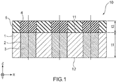
- Fig. 1 is a schematic cross-sectional view showing the configuration of a conductive member 10 according to the embodiment of the present invention.
- a horizontal direction in the cross-sectional view of the conductive member 10 shown in Fig. 1 is defined as an X-axis direction
- a direction perpendicular to the X-axis and extending through the drawing sheet is defined as a Y-axis direction
- a vertical direction perpendicular to the X-axis and the Y-axis is defined as a Z-axis direction.
- the cross-sectional view shown in Fig. 1 is a X-Z cross-sectional view of the conductive member 10 in accordance with the definitions described above.
- all the cross-sectional views of the conductive member 10 are X-Z cross-sectional views of the conductive member 10 unless otherwise specified.
- the conductive member 10 includes a glass substrate 1, a through hole 2 provided in the glass substrate 1, and an electrode portion 3 formed of a conductive material filled in the through hole 2.
- the conductive member 10 is formed of a conductive elastic material, and further includes a contact portion 4 and an insulation portion 5.
- the contact portion 4 is joined to an exposed part of the electrode portion 3 on a topside 11 of the glass substrate 1.
- the insulation portion 5 is formed of an insulating elastic material around the contact portion 4 on the topside 11 of the glass substrate 1.
- the configuration of the conductive member 10 is specifically described.
- the glass substrate 1 is a plate member made of hard glass.
- the glass substrate 1 secures a mechanical strength sufficient for the conductive member 10.
- through holes 2 are formed apart from each other at a predetermined pitch, and pass through the glass substrate 1 between the topside 11 and an underside 12 that are opposed to each other.
- the topside 11 of the glass substrate 1 refers to the surface closer to the contact surface of the conductive member 10 with an electrode of an electronic component to be tested.
- the underside 12 of the glass substrate 1 refers to the surface on which the conductive member 10 contacts a conducting portion of a testing device for electrical test.
- the electrode portion 3 is formed of a conductive material, for example, metal plating filled in the through hole 2.
- the electrode portion 3 is exposed to the outside of the glass substrate 1 from the topside 11 and the underside 12.
- the contact portion 4 is joined to the exposed part of the electrode portion 3 with conductive properties on the topside 11 of the glass substrate 1, so that the contact portion 4 is electrically connected to an exposed part of the electrode portion 3 on the underside 12.
- the insulation portion 5 insulates a plurality of contact portions 4 from each other, and prevents the contact portions 4 from electrically contacting each other.
- Fig. 2 is a schematic side view showing an example of arrangement of electrodes 101 of the electronic component 100 that is the tested object of an electrical test to be carried out using the conductive member 10.
- the electronic component 100 has a BGA package with hemispherical solders (solder balls) provided to serve as the electrodes 101 on the bottom portion of a package substrate.
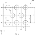
- Fig. 3 is a schematic plan view showing an example of arrangement of the electrodes 101 of the electronic component 100 that is the tested object of an electrical test to be carried out using the conductive member 10.
- a plurality of rows of the electrodes 101 arrayed at the predetermined pitch P1 in the X-axis direction are arranged as a first row R1, a second row R2, a third row R3, ... in the Y-axis direction.
- the rows of the electrodes 101 are arranged in a so-called staggered arrangement, in which the electrodes 101 on the second row R2 are alternately positioned in the middle between the electrodes 101 on the first row R1.
- a pitch P2 in the Y-axis direction between the electrodes 101 on the first row R1 and the electrodes 101 on the second row R2 is, for example, 48 ⁇ m.
- a pitch P3 in the X-axis direction between the electrodes 101 on the first row R1 and the electrodes 101 on the second row R2 is, for example, 27.5 ⁇ m.
- a pitch P4 in the Y-axis direction between the electrodes 101 on the first row R1 and the electrodes 101 on the third row R3 arrayed at the same pitch as those on the first row R1 is, for example, 96 ⁇ m.
- the conductive member 10 electrically connects the electrode 101 of the electronic component 100 with a conducting portion 201 of a testing device 200 to be described later through the electrode portion 3 formed in, and the contact portion 4 formed on, the glass substrate 1 which are described above.
- the conductive member 10 includes the contact portion 4 formed of a conductive elastic material, and can thus prevent the electrode 101 from being broken during an electrical test.
- the conductive member 10 includes the contact portion 4 and the insulation portion 5 on the glass substrate 1, and can thus bring the electrode 101 and the conducting portion 201 corresponding to each other into proper contact. Therefore, the conductive member 10 can accommodate downsizing of the electronic component 100 for an electrical test on the electronic component 100.
- the array of the electrodes 101, the numerical values of the pitch of the electrodes 101, and other factors in the electronic component 100 to be tested are not limited to those described above.
- the manufacturing method of a conductive member according to the present embodiment is performed by the following steps. First, in the present manufacturing method, on the glass substrate 1 formed with a plurality of through holes 2, an electrode-portion forming step of forming the electrode portion 3 in each of the through holes 2, and a resin-material layer forming step of forming a resin-material layer 6 on the topside 11 of the glass substrate 1 are performed.
- a via-hole forming step of forming a via hole 7 in the resin-material layer 6 formed on the glass substrate 1 at a location corresponding to the top of the electrode portion 3, a filling step of filling the via hole 7 with a conductive elastic material 40, and a semi-hardening step of semi-hardening the conductive elastic material 40 are performed.
- a separation step of separating the resin-material layer 6, an insulation-portion forming step of forming the insulation portion 5 on the topside 11 of the glass substrate 1 by using an insulating elastic material, and a hardening step of hardening the insulation portion 5 along with the conductive elastic material 40 are performed.
- the manufacturing method of the conductive member 10 is specifically described.
- the glass substrate 1 formed with the through holes 2 is prepared for manufacturing the conductive member 10.
- an alkali-free glass with the thickness t1 can be used, for example.
- the through holes 2 can be provided in the glass substrate 1 by using a CO 2 laser, a hydrogen fluoride laser, or other types of laser. Note that a specific method for forming the through holes 2 in the glass substrate 1 is not limited to the example described above.
- Fig. 4 is a schematic cross-sectional view showing an example of the glass substrate 1 of the conductive member 10.
- the through holes 2 are arrayed in a so-called staggered arrangement corresponding to the array of the electrodes 101 of the electronic component 100 described above, in which for example, the through holes 2 on the second row R2 are alternately positioned in the middle between the through holes 2 on the first row R1.
- the array of the through holes 2, and the pitch of the through holes 2 in the glass substrate 1 are not limited to the examples described above. That is, the array and other factors of the through holes 2 may not be the same as those of the electrodes 101 of the electronic component 100 as long as the array and other factors do not interfere with an electrical test on the electronic component 100.
- Fig. 5 is a schematic cross-sectional view for showing the manufacturing method of the conductive member, in which the electrode-portion forming step is shown.
- a process of filling the through hole 2 in the glass substrate 1 with a conductive material, for example, a plating process is performed on the conductive member 10 to form the electrode portion 3.
- the electrode portion 3 is formed from, for example, three plated layers including a first plated portion, a second plated portion, and a third plated portion.
- the first plated portion is formed to fill the inside of the through hole 2.
- the first plated portion is formed of, for example, copper plating.
- the second plated portion is formed on a part of the electrode portion 3 exposed from the through hole 2 on the topside 11 and the underside 12 of the glass substrate 1.
- the second plated portion is formed of, for example, electroless nickel plating.
- the second plated portion has a thickness of, for example, 2 ⁇ m.
- the third plated portion is formed on the surface of the second plated portion.
- the third plated portion is formed of, for example, electroless gold plating.
- the third plated portion has a thickness of, for example, 50 nm.
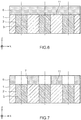
- Fig. 6 is a schematic cross-sectional view for showing the manufacturing method of the conductive member 10, in which the resin-material layer forming step is shown.
- the resin-material layer forming step the resin-material layer 6 is formed uniformly on the topside 11 of the glass substrate 1 having the electrode portion 3 formed in the through hole 2.
- the resin-material layer 6 is a resin film with photosensitivity that is, for example, a photosensitive polyimide film.
- the resin-material layer 6 has a thickness of, for example, 25 ⁇ m.
- the resin-material layer 6 is formed by laminating the photosensitive polyimide film described above on the topside 11 of the glass substrate 1, and then pressurizing and heating the laminated photosensitive polyimide film.
- Fig. 7 is a schematic cross-sectional view for showing the manufacturing method of the conductive member 10, in which the via-hole forming step is shown.
- the via hole 7 is formed in the resin-material layer 6 formed on the topside 11 of the glass substrate 1 at a location corresponding to the top of the electrode portion 3.
- the via hole 7 passes through the resin-material layer 6 between the topside of the resin-material layer 6 and the electrode portion 3.
- the via hole 7 is formed by performing a photolithography process on the resin-material layer 6 formed of the photosensitive polyimide film.
- the photolithography process in the via-hole forming step is performed in the following manner. First, by using a mask pattern through which the position of the via hole 7 to be formed is exposed to ultraviolet light, the resin-material layer 6 is exposed to the ultraviolet light to thereby form a latent image. After the exposure, the resin-material layer 6 undergoes thermal treatment. On the resin-material layer 6 having undergone the thermal treatment, a development process is performed using a developer, so that a portion with the latent image is removed and consequently the via hole 7 is formed.
- the photolithography process in the via-hole forming step is not limited to the example described above. Various methods can be used.
- Fig. 8 is a schematic cross-sectional view for showing the manufacturing method of the conductive member 10, in which the filling step is shown.
- the via hole 7 is filled with the conductive elastic material 40 to form the contact portion 4 within the via hole 7.
- the conductive elastic material 40 is formed by, for example, including particles with conductive properties (hereinafter, referred to as "conductive particles") in a silicone rubber serving as a binder.
- conductive particles particles with conductive properties
- the conductive elastic material 40 with respect to 100 parts-by-weight of the above silicone rubber, 900 parts-by-weight of the above conductive particles are combined and mixed with the silicone rubber into a paste.
- the conductive elastic material 40 is squeegeed by using a rubber blade, and thus filled in the via hole 7.
- the conductive elastic material 40 filled in the via hole 7 is semi-hardened by, for example, primary vulcanization at a temperature of 100°C for 30 minutes.
- Fig. 9 is a schematic cross-sectional view for showing the manufacturing method of the conductive member 10, in which the separation step is shown.
- Fig. 9 shows the glass substrate 1 after the resin-material layer 6 has been separated.
- the resin-material layer 6 shown in Fig. 8 and other drawings is separated from the topside 11 of the glass substrate 1 by an etching process.
- a specific etching process is performed by soaking the glass substrate 1 having the resin-material layer 6 affixed thereto in a solution with a concentration of tetramethylammonium hydroxide (TMAH) of 2.38% for 30 minutes.
- TMAH tetramethylammonium hydroxide
- the resin-material layer 6 is separated, and consequently the semi-hardened conductive elastic material 40 only remains at the position atop the electrode portion 3 on the topside 11 of the glass substrate 1.
- This semi-hardened conductive elastic material 40 becomes a conducting rubber pillar 41 that has a columnar or substantially columnar shape and that functions as the contact portion 4 after manufacturing of the conductive member 10 has been completed.
- Fig. 10 is a schematic cross-sectional view for showing the manufacturing method of the conductive member 10, in which the insulation-portion forming step is shown.
- the insulation-portion forming step on the topside 11 of the glass substrate 1 formed with the conducting rubber pillar 41, droplets of an insulating elastic material 50, such as a binder silicone rubber that does not include conductive particles or other conductive material, are dropped around the conducting rubber pillar 41 to form the insulation portion 5.
- an insulating elastic material 50 such as a binder silicone rubber that does not include conductive particles or other conductive material
- Fig. 11 is a schematic cross-sectional view for showing the manufacturing method of the conductive member 10, in which the hardening step is shown.
- a flat plate 20 is used, for example, to apply a load from above to the conducting rubber pillar 41 and the insulating elastic material 50 formed on the topside 11 of the glass substrate 1.
- a release film 21 is affixed to a contact surface of the flat plate 20 with the conducting rubber pillar 41 and the insulating elastic material 50.
- the conducting rubber pillar 41 and the insulating elastic material 50 are heated at a predetermined temperature (for example, 150°C) for a predetermined time (for example, two hours).
- a predetermined temperature for example, 150°C
- a predetermined time for example, two hours.
- the conducting rubber pillar 41 and the insulating elastic material 50 become hardened, and then the contact portion 4 that is electrically conducted with the electrode portion 3, and the insulation portion 5 that insulates the contact portions 4 from each other are formed on the topside 11 of the glass substrate 1.
- manufacturing of the conductive member 10 shown in Fig. 1 is completed.
- Fig. 12 is a schematic cross-sectional view showing an example of electrical test to be carried out on the electronic component 100 by using the conductive member 10.
- the conductive member 10 is interposed between the electrode 101 and the conducting portion 201. That is, in the conductive member 10, the contact portion 4 contacts the electrode 101, while the electrode portion 3 exposed on the underside 12 of the glass substrate 1 contacts the conducting portion 201.
- the value of electrical resistance of the conductive member 10 is measured using a gold-plated current-carrying probe needle as an equivalent to the electrode 101 of the electronic component 100 with an electrode diameter of 25 ⁇ m.
- the needle is applied with a load and brought into contact with the electrode portion 3 and the contact portion 4. This results in the value of electrical resistance of 100 m ⁇ relative to a load of 1 gf applied by the needle.
- a conductive member for electrical test that has a proper value of electrical resistance can be obtained.
- the conductive member 10 includes the contact portion 4 formed of a conductive elastic material on the topside 11 of the glass substrate 1 atop the electrode portion 3, and can thus protect the electrode 101 from being broken during an electrical test.
- the conductive member 10 includes the contact portion 4 formed of a conductive elastic material, and the insulation portion 5 formed of an insulating elastic material on the hard glass substrate 1. With this configuration, the conductive member 10 can obtain a mechanical strength (rigidity) sufficient for a pressing force applied by the testing device 200 during an electrical test.
- the conductive member 10 includes the electrode portion 3 in the through hole 2 provided in the glass substrate 1, and further includes the contact portion 4 formed by the photolithography process.
- the conductive member 10 can bring the electrode 101 and the conducting portion 201 into proper contact with each other even during an electrical test on the electronic component 100 that is downsized with a reduced pitch of the electrodes 101.
- the conductive member 10 for electrical test that can accommodate downsizing of the electronic component 100, and the manufacturing method of the conductive member 10 can be provided.
- the present invention is not limited to the manufacturing method of a conductive member, or the conductive member 10 according to the above embodiment of the present invention.
- the present invention includes various aspects within the concept and claims of the present invention.
- Each component may be appropriately and optionally combined to solve or provide at least part of the above-described problems or effects.
- the shape, material, arrangement, size, and other factors of each component according to the above embodiment may be appropriately changed depending on a specific use of the present invention.
Landscapes
- Engineering & Computer Science (AREA)
- Manufacturing & Machinery (AREA)
- Microelectronics & Electronic Packaging (AREA)
- Physics & Mathematics (AREA)
- General Physics & Mathematics (AREA)
- Measuring Leads Or Probes (AREA)
- Manufacturing Of Electrical Connectors (AREA)
- Structure Of Printed Boards (AREA)
Abstract
Description
- The present invention relates to a manufacturing method of a conductive member.
- An electrical test to check for a conducting state of an electrode of an electronic component such as a semiconductor integrated circuit is commonly known as bringing the above electrode into contact with a conducting portion of a testing device. A conductive member is commonly known as being interposed between the above electrode to be tested and the above conducting portion when an electrical test is carried out, in consideration of protecting the above electrode, and bringing this electrode into proper contact with the above conducting portion (For example, see
Patent Literatures 1 and 2). -
Patent Literature 1 discloses a technique of an anisotropic conducting rubber sheet including a conducting portion within an electrically-insulating material, in which the conducting portion is electrically connectable to a terminal electrode of a tested object, and includes a connection portion provided with an engaged portion with which the terminal electrode of the tested object is engaged. -
Patent Literature 2 discloses a technique configured to include an elastic conducting sheet including a first conducting portion and an insulating support portion that supports the first conducting portion while insulating the first conducting portion from the adjacent first conducting portion, a support sheet affixed to the elastic conducting sheet and formed with a through hole at a position corresponding to a terminal of a tested device, and a second conducting portion located within the through hole on the support sheet with a large number of second conductive particles located in a thickness direction within an elastic material of the second conducting portion. -
- Patent Literature 1:
Japanese Patent Application Publication No. H11-214594 - Patent Literature 2: National Publication of
International Patent Application No. 2015-501427 - Electronic components that are the object to be electrically tested have been increasingly downsized. As a technique to downsize the electronic components, a BGA (Ball grid array) package is commonly known, for example. In the BGA package, a semiconductor chip is mounted on a package substrate, and hemispherical solders (solder balls) are provided to serve as electrodes at the bottom portion of the package substrate. In an electronic component including the BGA package, a solder-ball pitch, that is, an electrode pitch can be set to, for example, approximately 500 µm, so that the connection area of the electrodes with an electronic circuit substrate can be relatively small.
- It is conceivable that as performance of the recent electronic components becomes more advanced, packages are further downsized with more highly-dense integration in the package, and accordingly the electrode pitch is further reduced to, for example, 55 µm.
- However, in a case where an electrical test is carried out on an electronic component with such a reduced electrode pitch as described above, it is difficult for the conventional techniques including those disclosed in
Patent Literatures - The present invention has been made in view of the above problems, and it is an object of the present invention to provide a manufacturing method of a conductive member for electrical test that can accommodate downsizing of an electronic component.
- To achieve the above object, a manufacturing method of a conductive member according to the present invention includes: an electrode-portion forming step of, on a glass substrate formed with a plurality of through holes at a predetermined pitch, forming an electrode portion in each of the through holes; a resin-material layer forming step of forming a resin-material layer on a topside of the glass substrate; a via-hole forming step of forming a via hole in a resin-material layer formed on the glass substrate at a position atop the electrode portion; a filling step of filling the via hole with a conductive elastic material; a semi-hardening step of semi-hardening the conductive elastic material; a separation step of separating the resin-material layer; an insulation-portion forming step of forming an insulation portion on a topside of the glass substrate by using an insulating elastic material; and a hardening step of hardening the insulation portion along with the conductive elastic material.
- In the manufacturing method of a conductive member according to one aspect of the present invention, the resin-material layer is formed of a resin material with photosensitivity, and in the via-hole forming step, the via hole is formed by performing a photolithography process on the resin-material layer at a position atop the electrode portion.
- In the manufacturing method of a conductive member according to one aspect of the present invention, the resin-material layer is separated from a topside of the glass substrate by an etching process.
- In the manufacturing method of a conductive member according to one aspect of the present invention, the insulating elastic material is a silicone rubber, and in the hardening step, a step of applying a load to the conductive elastic material and the insulation portion, and a step of heating the conductive elastic material and the insulation portion at a predetermined temperature for a predetermined time are performed to harden the conductive elastic material and the insulation portion.
- According to the present invention, a manufacturing method of a conductive member for electrical test can be provided, in which the conductive member can accommodate downsizing of an electronic component.
-
- [
Fig. 1 ] A schematic cross-sectional view showing the configuration of a conductive member according to an embodiment of the present invention. - [
Fig. 2 ] A schematic side view showing an example of arrangement of electrodes in an electronic component that is the tested object of an electrical test to be carried out using the conductive member shown inFig. 1 . - [
Fig. 3 ] A schematic plan view showing an example of arrangement of the electrodes in the electronic component that is the tested object of an electrical test to be carried out using the conductive member shown inFig. 1 . - [
Fig. 4 ] A schematic cross-sectional view showing an example of a glass substrate of the conductive member shown inFig. 1 . - [
Fig. 5 ] A schematic cross-sectional view for showing a manufacturing method of the conductive member shown inFig. 1 , in which an electrode-portion forming step is shown. - [
Fig. 6 ] A schematic cross-sectional view for showing the manufacturing method of the conductive member shown inFig. 1 , in which a resin-material layer forming step is shown. - [
Fig. 7 ] A schematic cross-sectional view for showing the manufacturing method of the conductive member shown inFig. 1 , in which a via-hole forming step is shown. - [
Fig. 8 ] A schematic cross-sectional view for showing the manufacturing method of the conductive member shown inFig. 1 , in which a filling step is shown. - [
Fig. 9 ] A schematic cross-sectional view for showing the manufacturing method of the conductive member shown inFig. 1 , in which a separation step is shown. - [
Fig. 10 ] A schematic cross-sectional view for showing the manufacturing method of the conductive member shown inFig. 1 , in which an insulation-portion forming step is shown. - [
Fig. 11 ] A schematic cross-sectional view for showing the manufacturing method of the conductive member shown inFig. 1 , in which a hardening step is shown. - [
Fig. 12 ] A schematic cross-sectional view showing an example of electrical test to be carried out on an electronic component by using the conductive member shown inFig. 1 . - Hereinafter, a manufacturing method of a conductive member according to an embodiment of the present invention, and the conductive member will be described with reference to the drawings.
- A conductive member according to one embodiment of the present invention is now described.
-
Fig. 1 is a schematic cross-sectional view showing the configuration of aconductive member 10 according to the embodiment of the present invention. In the following descriptions, a horizontal direction in the cross-sectional view of theconductive member 10 shown inFig. 1 is defined as an X-axis direction, a direction perpendicular to the X-axis and extending through the drawing sheet is defined as a Y-axis direction, and a vertical direction perpendicular to the X-axis and the Y-axis is defined as a Z-axis direction. That is, the cross-sectional view shown inFig. 1 is a X-Z cross-sectional view of theconductive member 10 in accordance with the definitions described above. In addition, in the following descriptions, all the cross-sectional views of theconductive member 10 are X-Z cross-sectional views of theconductive member 10 unless otherwise specified. - As shown in
Fig. 1 , theconductive member 10 includes aglass substrate 1, a throughhole 2 provided in theglass substrate 1, and anelectrode portion 3 formed of a conductive material filled in the throughhole 2. Theconductive member 10 is formed of a conductive elastic material, and further includes acontact portion 4 and aninsulation portion 5. Thecontact portion 4 is joined to an exposed part of theelectrode portion 3 on atopside 11 of theglass substrate 1. Theinsulation portion 5 is formed of an insulating elastic material around thecontact portion 4 on thetopside 11 of theglass substrate 1. Hereinafter, the configuration of theconductive member 10 is specifically described. - The
glass substrate 1 is a plate member made of hard glass. Theglass substrate 1 secures a mechanical strength sufficient for theconductive member 10. Theglass substrate 1 has a thickness t1, for example, t1 = 100 to 300 µm. In theglass substrate 1, throughholes 2 are formed apart from each other at a predetermined pitch, and pass through theglass substrate 1 between thetopside 11 and anunderside 12 that are opposed to each other. Thetopside 11 of theglass substrate 1 refers to the surface closer to the contact surface of theconductive member 10 with an electrode of an electronic component to be tested. Theunderside 12 of theglass substrate 1 refers to the surface on which theconductive member 10 contacts a conducting portion of a testing device for electrical test. - As described above, the
electrode portion 3 is formed of a conductive material, for example, metal plating filled in the throughhole 2. Theelectrode portion 3 is exposed to the outside of theglass substrate 1 from thetopside 11 and theunderside 12. An exposed part of theelectrode portion 3, exposed to the outside from theunderside 12, contacts the conducting portion of the testing device (not shown). - The
contact portion 4 is joined to the exposed part of theelectrode portion 3 with conductive properties on thetopside 11 of theglass substrate 1, so that thecontact portion 4 is electrically connected to an exposed part of theelectrode portion 3 on theunderside 12. Theinsulation portion 5 insulates a plurality ofcontact portions 4 from each other, and prevents thecontact portions 4 from electrically contacting each other. Thecontact portion 4 and theinsulation portion 5 have a thickness of, for example, t2 = 25 µm. - Next, an
electrode 101 of anelectronic component 100, to be contacted by theconductive member 10 during an electrical test, is described. -
Fig. 2 is a schematic side view showing an example of arrangement ofelectrodes 101 of theelectronic component 100 that is the tested object of an electrical test to be carried out using theconductive member 10. As shown inFig. 2 , in an array of theelectrodes 101, a predetermined pitch P1 (for example, P1 = 55 µm) is provided in the X-axis direction. Theelectronic component 100 has a BGA package with hemispherical solders (solder balls) provided to serve as theelectrodes 101 on the bottom portion of a package substrate. -
Fig. 3 is a schematic plan view showing an example of arrangement of theelectrodes 101 of theelectronic component 100 that is the tested object of an electrical test to be carried out using theconductive member 10. As shown inFig. 3 , in theelectronic component 100, a plurality of rows of theelectrodes 101 arrayed at the predetermined pitch P1 in the X-axis direction are arranged as a first row R1, a second row R2, a third row R3, ... in the Y-axis direction. For example, the rows of theelectrodes 101 are arranged in a so-called staggered arrangement, in which theelectrodes 101 on the second row R2 are alternately positioned in the middle between theelectrodes 101 on the first row R1. A pitch P2 in the Y-axis direction between theelectrodes 101 on the first row R1 and theelectrodes 101 on the second row R2 is, for example, 48 µm. A pitch P3 in the X-axis direction between theelectrodes 101 on the first row R1 and theelectrodes 101 on the second row R2 is, for example, 27.5 µm. A pitch P4 in the Y-axis direction between theelectrodes 101 on the first row R1 and theelectrodes 101 on the third row R3 arrayed at the same pitch as those on the first row R1 is, for example, 96 µm. - The
conductive member 10 electrically connects theelectrode 101 of theelectronic component 100 with a conductingportion 201 of atesting device 200 to be described later through theelectrode portion 3 formed in, and thecontact portion 4 formed on, theglass substrate 1 which are described above. Theconductive member 10 includes thecontact portion 4 formed of a conductive elastic material, and can thus prevent theelectrode 101 from being broken during an electrical test. Theconductive member 10 includes thecontact portion 4 and theinsulation portion 5 on theglass substrate 1, and can thus bring theelectrode 101 and the conductingportion 201 corresponding to each other into proper contact. Therefore, theconductive member 10 can accommodate downsizing of theelectronic component 100 for an electrical test on theelectronic component 100. - Note that in the present invention, the array of the
electrodes 101, the numerical values of the pitch of theelectrodes 101, and other factors in theelectronic component 100 to be tested are not limited to those described above. - A manufacturing method of the
conductive member 10 according to one embodiment of the present invention is now described. - The manufacturing method of a conductive member according to the present embodiment is performed by the following steps. First, in the present manufacturing method, on the
glass substrate 1 formed with a plurality of throughholes 2, an electrode-portion forming step of forming theelectrode portion 3 in each of the throughholes 2, and a resin-material layer forming step of forming a resin-material layer 6 on thetopside 11 of theglass substrate 1 are performed. In the present manufacturing method, after the resin-material layer forming step, a via-hole forming step of forming a viahole 7 in the resin-material layer 6 formed on theglass substrate 1 at a location corresponding to the top of theelectrode portion 3, a filling step of filling the viahole 7 with a conductiveelastic material 40, and a semi-hardening step of semi-hardening the conductiveelastic material 40 are performed. In the present manufacturing method, after the semi-hardening step, a separation step of separating the resin-material layer 6, an insulation-portion forming step of forming theinsulation portion 5 on thetopside 11 of theglass substrate 1 by using an insulating elastic material, and a hardening step of hardening theinsulation portion 5 along with the conductiveelastic material 40 are performed. Hereinafter, the manufacturing method of theconductive member 10 is specifically described. - In the present manufacturing method, the
glass substrate 1 formed with the throughholes 2 is prepared for manufacturing theconductive member 10. As theglass substrate 1, an alkali-free glass with the thickness t1 can be used, for example. The throughholes 2 can be provided in theglass substrate 1 by using a CO2 laser, a hydrogen fluoride laser, or other types of laser. Note that a specific method for forming the throughholes 2 in theglass substrate 1 is not limited to the example described above. -
Fig. 4 is a schematic cross-sectional view showing an example of theglass substrate 1 of theconductive member 10. As shown inFig. 4 , the throughholes 2 pass through theglass substrate 1 between the topside 11 and theunderside 12, and have a predetermined hole diameter d (for example, d = 28 µm). The throughholes 2 are formed corresponding to the array of theelectrodes 101 of theelectronic component 100 shown inFigs. 2 and3 as the object on which an electrical test is carried out using theconductive member 10. That is, in an array of the throughholes 2, the predetermined pitch P1 (for example, P1 = 55 µm) is provided in the X-axis direction in the same manner as theelectrodes 101 of theelectronic component 100. Also in the Y-axis direction, the throughholes 2 are arrayed in a so-called staggered arrangement corresponding to the array of theelectrodes 101 of theelectronic component 100 described above, in which for example, the throughholes 2 on the second row R2 are alternately positioned in the middle between the throughholes 2 on the first row R1. - Note that in the present invention, the array of the through
holes 2, and the pitch of the throughholes 2 in theglass substrate 1 are not limited to the examples described above. That is, the array and other factors of the throughholes 2 may not be the same as those of theelectrodes 101 of theelectronic component 100 as long as the array and other factors do not interfere with an electrical test on theelectronic component 100. - First, an electrode-portion forming step in the manufacturing method of the
conductive member 10 according to the present embodiment is described. -
Fig. 5 is a schematic cross-sectional view for showing the manufacturing method of the conductive member, in which the electrode-portion forming step is shown. As shown inFig. 5 , in the electrode-portion forming step, a process of filling the throughhole 2 in theglass substrate 1 with a conductive material, for example, a plating process is performed on theconductive member 10 to form theelectrode portion 3. Theelectrode portion 3 is formed from, for example, three plated layers including a first plated portion, a second plated portion, and a third plated portion. - The first plated portion is formed to fill the inside of the through
hole 2. The first plated portion is formed of, for example, copper plating. - The second plated portion is formed on a part of the
electrode portion 3 exposed from the throughhole 2 on the topside 11 and theunderside 12 of theglass substrate 1. The second plated portion is formed of, for example, electroless nickel plating. The second plated portion has a thickness of, for example, 2 µm. - The third plated portion is formed on the surface of the second plated portion. The third plated portion is formed of, for example, electroless gold plating. The third plated portion has a thickness of, for example, 50 nm.
- Next, a resin-material layer forming step in the manufacturing method of the
conductive member 10 according to the present embodiment is described. -
Fig. 6 is a schematic cross-sectional view for showing the manufacturing method of theconductive member 10, in which the resin-material layer forming step is shown. As shown inFig. 6 , in the resin-material layer forming step, the resin-material layer 6 is formed uniformly on thetopside 11 of theglass substrate 1 having theelectrode portion 3 formed in the throughhole 2. The resin-material layer 6 is a resin film with photosensitivity that is, for example, a photosensitive polyimide film. The resin-material layer 6 has a thickness of, for example, 25 µm. The resin-material layer 6 is formed by laminating the photosensitive polyimide film described above on thetopside 11 of theglass substrate 1, and then pressurizing and heating the laminated photosensitive polyimide film. - Next, a via-hole forming step in the manufacturing method of the
conductive member 10 according to the present embodiment is described. -
Fig. 7 is a schematic cross-sectional view for showing the manufacturing method of theconductive member 10, in which the via-hole forming step is shown. As shown inFig. 7 , in the via-hole forming step, the viahole 7 is formed in the resin-material layer 6 formed on thetopside 11 of theglass substrate 1 at a location corresponding to the top of theelectrode portion 3. The viahole 7 passes through the resin-material layer 6 between the topside of the resin-material layer 6 and theelectrode portion 3. In the via-hole forming step, the viahole 7 is formed by performing a photolithography process on the resin-material layer 6 formed of the photosensitive polyimide film. - For example, the photolithography process in the via-hole forming step is performed in the following manner. First, by using a mask pattern through which the position of the via
hole 7 to be formed is exposed to ultraviolet light, the resin-material layer 6 is exposed to the ultraviolet light to thereby form a latent image. After the exposure, the resin-material layer 6 undergoes thermal treatment. On the resin-material layer 6 having undergone the thermal treatment, a development process is performed using a developer, so that a portion with the latent image is removed and consequently the viahole 7 is formed. The photolithography process in the via-hole forming step is not limited to the example described above. Various methods can be used. - Next, a filling step in the manufacturing method of the
conductive member 10 according to the present embodiment is described. -
Fig. 8 is a schematic cross-sectional view for showing the manufacturing method of theconductive member 10, in which the filling step is shown. As shown inFig. 8 , in the filling step, the viahole 7 is filled with the conductiveelastic material 40 to form thecontact portion 4 within the viahole 7. The conductiveelastic material 40 is formed by, for example, including particles with conductive properties (hereinafter, referred to as "conductive particles") in a silicone rubber serving as a binder. For example, as the conductive particles, nickel particles with an average particle diameter of 2.5 µm, which are coated with gold plating at a weight ratio of 30% with a film thickness of 50 nm, are used. In the conductiveelastic material 40, with respect to 100 parts-by-weight of the above silicone rubber, 900 parts-by-weight of the above conductive particles are combined and mixed with the silicone rubber into a paste. The conductiveelastic material 40 is squeegeed by using a rubber blade, and thus filled in the viahole 7. - Next, a semi-hardening step in the manufacturing method of the
conductive member 10 according to the present embodiment is described. - The conductive
elastic material 40 filled in the viahole 7 is semi-hardened by, for example, primary vulcanization at a temperature of 100°C for 30 minutes. - Next, a separation step in the manufacturing method of the
conductive member 10 according to the present embodiment is described. -
Fig. 9 is a schematic cross-sectional view for showing the manufacturing method of theconductive member 10, in which the separation step is shown.Fig. 9 shows theglass substrate 1 after the resin-material layer 6 has been separated. In the separation step, the resin-material layer 6 shown inFig. 8 and other drawings is separated from thetopside 11 of theglass substrate 1 by an etching process. For example, a specific etching process is performed by soaking theglass substrate 1 having the resin-material layer 6 affixed thereto in a solution with a concentration of tetramethylammonium hydroxide (TMAH) of 2.38% for 30 minutes. The resin-material layer 6 is separated from thetopside 11 of theglass substrate 1 by performing the etching process. The resin-material layer 6 is separated, and consequently the semi-hardened conductiveelastic material 40 only remains at the position atop theelectrode portion 3 on thetopside 11 of theglass substrate 1. This semi-hardened conductiveelastic material 40 becomes a conductingrubber pillar 41 that has a columnar or substantially columnar shape and that functions as thecontact portion 4 after manufacturing of theconductive member 10 has been completed. - Next, an insulation-portion forming step in the manufacturing method of the
conductive member 10 according to the present embodiment is described. -
Fig. 10 is a schematic cross-sectional view for showing the manufacturing method of theconductive member 10, in which the insulation-portion forming step is shown. In the insulation-portion forming step, on thetopside 11 of theglass substrate 1 formed with the conductingrubber pillar 41, droplets of an insulatingelastic material 50, such as a binder silicone rubber that does not include conductive particles or other conductive material, are dropped around the conductingrubber pillar 41 to form theinsulation portion 5. - Lastly, a hardening step in the manufacturing method of the
conductive member 10 according to the present embodiment is described. -
Fig. 11 is a schematic cross-sectional view for showing the manufacturing method of theconductive member 10, in which the hardening step is shown. In the hardening step, a flat plate 20 is used, for example, to apply a load from above to the conductingrubber pillar 41 and the insulatingelastic material 50 formed on thetopside 11 of theglass substrate 1. Arelease film 21 is affixed to a contact surface of the flat plate 20 with the conductingrubber pillar 41 and the insulatingelastic material 50. In the hardening step, in a state where the conductingrubber pillar 41 and the insulatingelastic material 50 are applied with a load from above, the conductingrubber pillar 41 and the insulatingelastic material 50 are heated at a predetermined temperature (for example, 150°C) for a predetermined time (for example, two hours). The steps described above are performed, and consequently on thetopside 11 of theglass substrate 1, the insulatingelastic material 50 becomes hardened and theinsulation portion 5 is formed. Along with that, the semi-hardened conductingrubber pillar 41 becomes fully hardened and thereby thecontact portion 4 is formed. - Through the hardening step, the conducting
rubber pillar 41 and the insulatingelastic material 50 become hardened, and then thecontact portion 4 that is electrically conducted with theelectrode portion 3, and theinsulation portion 5 that insulates thecontact portions 4 from each other are formed on thetopside 11 of theglass substrate 1. Thus, manufacturing of theconductive member 10 shown inFig. 1 is completed. - Next, an example of electrical test using the
conductive member 10 explained above is described. -
Fig. 12 is a schematic cross-sectional view showing an example of electrical test to be carried out on theelectronic component 100 by using theconductive member 10. As shown inFig. 12 , when an electrical test is carried out to test a conducting state of theelectrode 101 of theelectronic component 100 such as a semiconductor integrated circuit by means of bringing theelectrode 101 into contact with the conductingportion 201 of thetesting device 200, theconductive member 10 is interposed between theelectrode 101 and the conductingportion 201. That is, in theconductive member 10, thecontact portion 4 contacts theelectrode 101, while theelectrode portion 3 exposed on theunderside 12 of theglass substrate 1 contacts the conductingportion 201. - For the purpose of evaluating the
conductive member 10 according to the present embodiment, the value of electrical resistance of theconductive member 10 is measured using a gold-plated current-carrying probe needle as an equivalent to theelectrode 101 of theelectronic component 100 with an electrode diameter of 25 µm. The needle is applied with a load and brought into contact with theelectrode portion 3 and thecontact portion 4. This results in the value of electrical resistance of 100 mΩ relative to a load of 1 gf applied by the needle. According to theconductive member 10, a conductive member for electrical test that has a proper value of electrical resistance can be obtained. - The
conductive member 10 includes thecontact portion 4 formed of a conductive elastic material on thetopside 11 of theglass substrate 1 atop theelectrode portion 3, and can thus protect theelectrode 101 from being broken during an electrical test. - The
conductive member 10 includes thecontact portion 4 formed of a conductive elastic material, and theinsulation portion 5 formed of an insulating elastic material on thehard glass substrate 1. With this configuration, theconductive member 10 can obtain a mechanical strength (rigidity) sufficient for a pressing force applied by thetesting device 200 during an electrical test. Theconductive member 10 includes theelectrode portion 3 in the throughhole 2 provided in theglass substrate 1, and further includes thecontact portion 4 formed by the photolithography process. Thus, even when the distance between theelectrode portions 3 adjacent to each other is minute, while the distance between thecontact portions 4 adjacent to each other is minute, the positional accuracy of both theelectrode portions 3 and thecontact portions 4 can still be obtained. That is, theconductive member 10 can bring theelectrode 101 and the conductingportion 201 into proper contact with each other even during an electrical test on theelectronic component 100 that is downsized with a reduced pitch of theelectrodes 101. - Therefore, according to the present embodiment, the
conductive member 10 for electrical test that can accommodate downsizing of theelectronic component 100, and the manufacturing method of theconductive member 10 can be provided. - While the embodiment of the present invention has been described above, the present invention is not limited to the manufacturing method of a conductive member, or the
conductive member 10 according to the above embodiment of the present invention. The present invention includes various aspects within the concept and claims of the present invention. Each component may be appropriately and optionally combined to solve or provide at least part of the above-described problems or effects. For example, the shape, material, arrangement, size, and other factors of each component according to the above embodiment may be appropriately changed depending on a specific use of the present invention. -
- 1
- glass substrate,
- 2
- through hole,
- 3
- electrode portion,
- 4
- contact portion,
- 5
- insulation portion,
- 6
- resin-material layer,
- 7
- via hole,
- 10
- conductive member,
- 11
- topside,
- 12
- underside,
- 20
- flat plate,
- 21
- release film,
- 40
- conductive elastic material,
- 41
- conducting rubber pillar,
- 100
- electronic component,
- 101
- electrode,
- 200
- testing device,
- 201
- conducting portion
Claims (4)
- A manufacturing method of a conductive member, the method comprising:an electrode-portion forming step of, on a glass substrate formed with a plurality of through holes, forming an electrode portion in each of the through holes;a resin-material layer forming step of forming a resin-material layer on a topside of the glass substrate;a via-hole forming step of forming a via hole in a resin-material layer formed on the glass substrate at a position atop the electrode portion;a filling step of filling the via hole with a conductive elastic material;a semi-hardening step of semi-hardening the conductive elastic material;a separation step of separating the resin-material layer;an insulation-portion forming step of forming an insulation portion on a topside of the glass substrate by using an insulating elastic material; anda hardening step of hardening the insulation portion along with the conductive elastic material.
- The manufacturing method of a conductive member according to claim 1, whereinthe resin-material layer is formed of a resin material with photosensitivity, andin the via-hole forming step, the via hole is formed by performing a photolithography process on the resin-material layer at a position atop the electrode portion.
- The manufacturing method of a conductive member according to claim 1 or 2, wherein in the separation step, the resin-material layer is separated from a topside of the glass substrate by an etching process.
- The manufacturing method of a conductive member according to any of claims 1 to 3, whereinthe insulating elastic material is a silicone rubber, andin the hardening step, a step of applying a load to the conductive elastic material and the insulation portion, and a step of heating the conductive elastic material and the insulation portion at a predetermined temperature for a predetermined time are performed to harden the conductive elastic material and the insulation portion.
Applications Claiming Priority (2)
| Application Number | Priority Date | Filing Date | Title |
|---|---|---|---|
| JP2018208166 | 2018-11-05 | ||
| PCT/JP2019/041140 WO2020095656A1 (en) | 2018-11-05 | 2019-10-18 | Method for manufacturing conductive member |
Publications (1)
| Publication Number | Publication Date |
|---|---|
| EP3879567A1 true EP3879567A1 (en) | 2021-09-15 |
Family
ID=70612385
Family Applications (1)
| Application Number | Title | Priority Date | Filing Date |
|---|---|---|---|
| EP19881136.6A Withdrawn EP3879567A1 (en) | 2018-11-05 | 2019-10-18 | Method for manufacturing conductive member |
Country Status (7)
| Country | Link |
|---|---|
| US (1) | US20210251086A1 (en) |
| EP (1) | EP3879567A1 (en) |
| JP (1) | JP6756996B1 (en) |
| KR (1) | KR20210032479A (en) |
| CN (1) | CN112585748A (en) |
| TW (1) | TWI721629B (en) |
| WO (1) | WO2020095656A1 (en) |
Families Citing this family (1)
| Publication number | Priority date | Publication date | Assignee | Title |
|---|---|---|---|---|
| KR102310726B1 (en) * | 2021-03-05 | 2021-10-12 | (주)위드멤스 | Flexible contactor and method for manufacturing the same |
Family Cites Families (13)
| Publication number | Priority date | Publication date | Assignee | Title |
|---|---|---|---|---|
| JP2890911B2 (en) * | 1991-07-25 | 1999-05-17 | ジェイエスアール株式会社 | Circuit board device |
| JPH05218149A (en) * | 1992-02-04 | 1993-08-27 | Tokyo Electron Ltd | Probe device |
| JPH11214594A (en) | 1998-01-20 | 1999-08-06 | Jsr Corp | Anisotropic conductive rubber sheet |
| JP3455442B2 (en) * | 1998-10-30 | 2003-10-14 | 日本電信電話株式会社 | Wiring structure manufacturing method |
| JP3978905B2 (en) * | 1998-11-19 | 2007-09-19 | Jsr株式会社 | Anisotropic conductive laminate and process for producing the same |
| KR20070046033A (en) * | 2004-08-31 | 2007-05-02 | 제이에스알 가부시끼가이샤 | Anisotropic Conductive Connector for Wafer Inspection and Manufacturing Method and Application thereof |
| US8120188B2 (en) * | 2006-11-28 | 2012-02-21 | Panasonic Corporation | Electronic component mounting structure and method for manufacturing the same |
| JP2009115524A (en) * | 2007-11-05 | 2009-05-28 | Tokyo Electron Ltd | Intermediate structure manufacturing method and inspection apparatus |
| JP4951018B2 (en) * | 2009-03-30 | 2012-06-13 | 株式会社東芝 | Manufacturing method of semiconductor device |
| JP2012217136A (en) * | 2011-03-30 | 2012-11-08 | Nippon Dempa Kogyo Co Ltd | Manufacturing method of piezoelectric device and the piezoelectric device manufactured by the manufacturing method |
| KR101266124B1 (en) | 2012-04-03 | 2013-05-27 | 주식회사 아이에스시 | Test socket with high density conduction section and fabrication method thereof |
| CN114221146B (en) * | 2016-11-30 | 2024-11-22 | 迪睿合株式会社 | Conductive particle arrangement film, manufacturing method thereof, inspection probe unit, and conduction inspection method |
| JP6918518B2 (en) * | 2017-02-27 | 2021-08-11 | デクセリアルズ株式会社 | Electrical property inspection jig |
-
2019
- 2019-10-18 CN CN201980054268.4A patent/CN112585748A/en active Pending
- 2019-10-18 US US17/270,752 patent/US20210251086A1/en not_active Abandoned
- 2019-10-18 EP EP19881136.6A patent/EP3879567A1/en not_active Withdrawn
- 2019-10-18 KR KR1020217004718A patent/KR20210032479A/en not_active Ceased
- 2019-10-18 WO PCT/JP2019/041140 patent/WO2020095656A1/en not_active Ceased
- 2019-10-18 JP JP2020529390A patent/JP6756996B1/en active Active
- 2019-11-04 TW TW108139862A patent/TWI721629B/en active
Also Published As
| Publication number | Publication date |
|---|---|
| TWI721629B (en) | 2021-03-11 |
| US20210251086A1 (en) | 2021-08-12 |
| WO2020095656A1 (en) | 2020-05-14 |
| JP6756996B1 (en) | 2020-09-16 |
| CN112585748A (en) | 2021-03-30 |
| TW202032143A (en) | 2020-09-01 |
| JPWO2020095656A1 (en) | 2021-02-15 |
| KR20210032479A (en) | 2021-03-24 |
Similar Documents
| Publication | Publication Date | Title |
|---|---|---|
| CN101584033B (en) | Compliant microelectronic assembly and method thereof | |
| JP4862017B2 (en) | Relay board, manufacturing method thereof, probe card | |
| US6242935B1 (en) | Interconnect for testing semiconductor components and method of fabrication | |
| US11099227B2 (en) | Multilayer wiring base plate and probe card using the same | |
| CN101510543B (en) | Integrated semiconductor device | |
| CN101673694A (en) | Method for manufacturing space transformer of semiconductor test probe card | |
| US20080180118A1 (en) | Substrate for probe card assembly, method of manufacturing substrate for probe card assembly and method of inspecting semiconductor wafer | |
| JPH0680713B2 (en) | Wafer test probe card and method of manufacturing the same | |
| WO2007000799A1 (en) | Contactor, contact structure with the contactor, probe card, testing device, contact structure producing method, and contact structure producing apparatus | |
| JP4343256B1 (en) | Manufacturing method of semiconductor device | |
| JP2018141652A (en) | Inspection jig of electrical characteristic | |
| US20070126459A1 (en) | Method for testing semiconductor components using bonded electrical connections | |
| KR20060130683A (en) | Manufacturing method of semiconductor integrated circuit device | |
| CN109585317A (en) | Test equipment and test method | |
| JP4944982B2 (en) | Semiconductor wafer inspection method and semiconductor device manufacturing method | |
| US20210251086A1 (en) | Manufacturing method of conductive member | |
| US20070222465A1 (en) | Probe head with vertical probes, method for manufacturing the probe head and probe card using the probe head | |
| US8088634B2 (en) | Methods of adding pads and one or more interconnect layers to the passivated topside of a wafer including connections to at least a portion of the integrated circuit pads thereon | |
| KR20110087437A (en) | Silicon rubber connector and its manufacturing method | |
| US20110097856A1 (en) | Method of manufacturing wafer level package | |
| JP4081309B2 (en) | ELECTRONIC COMPONENT SOCKET, MANUFACTURING METHOD THEREOF, AND MOUNTING STRUCTURE USING ELECTRONIC COMPONENT SOCKET | |
| JP4492976B2 (en) | Semiconductor device | |
| JP3596499B2 (en) | Method for manufacturing semiconductor inspection device, semiconductor inspection device, and method for inspecting semiconductor device | |
| JP2004245671A (en) | Probe card and method for manufacturing the same, probe device, probe test method, and method for manufacturing semiconductor device | |
| KR100947916B1 (en) | Printed Circuit Boards for Probe Cards |
Legal Events
| Date | Code | Title | Description |
|---|---|---|---|
| STAA | Information on the status of an ep patent application or granted ep patent |
Free format text: STATUS: THE INTERNATIONAL PUBLICATION HAS BEEN MADE |
|
| PUAI | Public reference made under article 153(3) epc to a published international application that has entered the european phase |
Free format text: ORIGINAL CODE: 0009012 |
|
| STAA | Information on the status of an ep patent application or granted ep patent |
Free format text: STATUS: REQUEST FOR EXAMINATION WAS MADE |
|
| STAA | Information on the status of an ep patent application or granted ep patent |
Free format text: STATUS: THE APPLICATION HAS BEEN WITHDRAWN |
|
| 17P | Request for examination filed |
Effective date: 20210224 |
|
| AK | Designated contracting states |
Kind code of ref document: A1 Designated state(s): AL AT BE BG CH CY CZ DE DK EE ES FI FR GB GR HR HU IE IS IT LI LT LU LV MC MK MT NL NO PL PT RO RS SE SI SK SM TR |
|
| 18W | Application withdrawn |
Effective date: 20210827 |