EP3876344A1 - Antenna, array antenna, wireless communication module, and wireless communication device - Google Patents
Antenna, array antenna, wireless communication module, and wireless communication device Download PDFInfo
- Publication number
- EP3876344A1 EP3876344A1 EP19879002.4A EP19879002A EP3876344A1 EP 3876344 A1 EP3876344 A1 EP 3876344A1 EP 19879002 A EP19879002 A EP 19879002A EP 3876344 A1 EP3876344 A1 EP 3876344A1
- Authority
- EP
- European Patent Office
- Prior art keywords
- conductor
- feeding line
- feeding
- circuit
- antenna
- Prior art date
- Legal status (The legal status is an assumption and is not a legal conclusion. Google has not performed a legal analysis and makes no representation as to the accuracy of the status listed.)
- Withdrawn
Links
- 238000004891 communication Methods 0.000 title claims abstract description 42
- 239000004020 conductor Substances 0.000 claims abstract description 638
- 230000005855 radiation Effects 0.000 claims abstract description 179
- 239000000758 substrate Substances 0.000 claims description 6
- 230000005540 biological transmission Effects 0.000 claims description 3
- 238000003475 lamination Methods 0.000 claims description 3
- 239000000463 material Substances 0.000 description 34
- 230000005284 excitation Effects 0.000 description 12
- 230000006870 function Effects 0.000 description 9
- 230000008878 coupling Effects 0.000 description 8
- 238000010168 coupling process Methods 0.000 description 8
- 238000005859 coupling reaction Methods 0.000 description 8
- 239000011347 resin Substances 0.000 description 6
- 229920005989 resin Polymers 0.000 description 6
- 239000000470 constituent Substances 0.000 description 5
- 238000010586 diagram Methods 0.000 description 5
- 238000002955 isolation Methods 0.000 description 4
- 230000009467 reduction Effects 0.000 description 4
- 238000005516 engineering process Methods 0.000 description 3
- 239000007769 metal material Substances 0.000 description 3
- PXHVJJICTQNCMI-UHFFFAOYSA-N Nickel Chemical compound [Ni] PXHVJJICTQNCMI-UHFFFAOYSA-N 0.000 description 2
- KDLHZDBZIXYQEI-UHFFFAOYSA-N Palladium Chemical compound [Pd] KDLHZDBZIXYQEI-UHFFFAOYSA-N 0.000 description 2
- 239000004962 Polyamide-imide Substances 0.000 description 2
- 239000004697 Polyetherimide Substances 0.000 description 2
- 239000011230 binding agent Substances 0.000 description 2
- 229910010293 ceramic material Inorganic materials 0.000 description 2
- 229920001940 conductive polymer Polymers 0.000 description 2
- 239000003822 epoxy resin Substances 0.000 description 2
- 239000011521 glass Substances 0.000 description 2
- 239000000203 mixture Substances 0.000 description 2
- BASFCYQUMIYNBI-UHFFFAOYSA-N platinum Chemical compound [Pt] BASFCYQUMIYNBI-UHFFFAOYSA-N 0.000 description 2
- 230000010287 polarization Effects 0.000 description 2
- 229920002312 polyamide-imide Polymers 0.000 description 2
- 229920000647 polyepoxide Polymers 0.000 description 2
- 229920001225 polyester resin Polymers 0.000 description 2
- 239000004645 polyester resin Substances 0.000 description 2
- 229920001601 polyetherimide Polymers 0.000 description 2
- 229920001721 polyimide Polymers 0.000 description 2
- 239000009719 polyimide resin Substances 0.000 description 2
- 229920000642 polymer Polymers 0.000 description 2
- 229910000505 Al2TiO5 Inorganic materials 0.000 description 1
- VYZAMTAEIAYCRO-UHFFFAOYSA-N Chromium Chemical compound [Cr] VYZAMTAEIAYCRO-UHFFFAOYSA-N 0.000 description 1
- RYGMFSIKBFXOCR-UHFFFAOYSA-N Copper Chemical compound [Cu] RYGMFSIKBFXOCR-UHFFFAOYSA-N 0.000 description 1
- 229920000106 Liquid crystal polymer Polymers 0.000 description 1
- 239000004977 Liquid-crystal polymers (LCPs) Substances 0.000 description 1
- WHXSMMKQMYFTQS-UHFFFAOYSA-N Lithium Chemical compound [Li] WHXSMMKQMYFTQS-UHFFFAOYSA-N 0.000 description 1
- BUGBHKTXTAQXES-UHFFFAOYSA-N Selenium Chemical compound [Se] BUGBHKTXTAQXES-UHFFFAOYSA-N 0.000 description 1
- BQCADISMDOOEFD-UHFFFAOYSA-N Silver Chemical compound [Ag] BQCADISMDOOEFD-UHFFFAOYSA-N 0.000 description 1
- ATJFFYVFTNAWJD-UHFFFAOYSA-N Tin Chemical compound [Sn] ATJFFYVFTNAWJD-UHFFFAOYSA-N 0.000 description 1
- RTAQQCXQSZGOHL-UHFFFAOYSA-N Titanium Chemical compound [Ti] RTAQQCXQSZGOHL-UHFFFAOYSA-N 0.000 description 1
- 229910045601 alloy Inorganic materials 0.000 description 1
- 239000000956 alloy Substances 0.000 description 1
- 229910052782 aluminium Inorganic materials 0.000 description 1
- XAGFODPZIPBFFR-UHFFFAOYSA-N aluminium Chemical compound [Al] XAGFODPZIPBFFR-UHFFFAOYSA-N 0.000 description 1
- 229940024548 aluminum oxide Drugs 0.000 description 1
- 230000008901 benefit Effects 0.000 description 1
- 229910052793 cadmium Inorganic materials 0.000 description 1
- BDOSMKKIYDKNTQ-UHFFFAOYSA-N cadmium atom Chemical compound [Cd] BDOSMKKIYDKNTQ-UHFFFAOYSA-N 0.000 description 1
- 230000008859 change Effects 0.000 description 1
- 229910052804 chromium Inorganic materials 0.000 description 1
- 239000011651 chromium Substances 0.000 description 1
- 229910017052 cobalt Inorganic materials 0.000 description 1
- 239000010941 cobalt Substances 0.000 description 1
- GUTLYIVDDKVIGB-UHFFFAOYSA-N cobalt atom Chemical compound [Co] GUTLYIVDDKVIGB-UHFFFAOYSA-N 0.000 description 1
- 229910052802 copper Inorganic materials 0.000 description 1
- 239000010949 copper Substances 0.000 description 1
- PMHQVHHXPFUNSP-UHFFFAOYSA-M copper(1+);methylsulfanylmethane;bromide Chemical compound Br[Cu].CSC PMHQVHHXPFUNSP-UHFFFAOYSA-M 0.000 description 1
- 230000001419 dependent effect Effects 0.000 description 1
- 238000000151 deposition Methods 0.000 description 1
- KZHJGOXRZJKJNY-UHFFFAOYSA-N dioxosilane;oxo(oxoalumanyloxy)alumane Chemical compound O=[Si]=O.O=[Si]=O.O=[Al]O[Al]=O.O=[Al]O[Al]=O.O=[Al]O[Al]=O KZHJGOXRZJKJNY-UHFFFAOYSA-N 0.000 description 1
- 230000001747 exhibiting effect Effects 0.000 description 1
- 239000002241 glass-ceramic Substances 0.000 description 1
- PCHJSUWPFVWCPO-UHFFFAOYSA-N gold Chemical compound [Au] PCHJSUWPFVWCPO-UHFFFAOYSA-N 0.000 description 1
- 229910052737 gold Inorganic materials 0.000 description 1
- 239000010931 gold Substances 0.000 description 1
- 238000004898 kneading Methods 0.000 description 1
- 239000011133 lead Substances 0.000 description 1
- 229910052744 lithium Inorganic materials 0.000 description 1
- WPBNNNQJVZRUHP-UHFFFAOYSA-L manganese(2+);methyl n-[[2-(methoxycarbonylcarbamothioylamino)phenyl]carbamothioyl]carbamate;n-[2-(sulfidocarbothioylamino)ethyl]carbamodithioate Chemical compound [Mn+2].[S-]C(=S)NCCNC([S-])=S.COC(=O)NC(=S)NC1=CC=CC=C1NC(=S)NC(=O)OC WPBNNNQJVZRUHP-UHFFFAOYSA-L 0.000 description 1
- 239000011159 matrix material Substances 0.000 description 1
- 229910052751 metal Inorganic materials 0.000 description 1
- 239000002184 metal Substances 0.000 description 1
- 229910001092 metal group alloy Inorganic materials 0.000 description 1
- 238000000034 method Methods 0.000 description 1
- 239000010445 mica Substances 0.000 description 1
- 229910052618 mica group Inorganic materials 0.000 description 1
- 238000012986 modification Methods 0.000 description 1
- 230000004048 modification Effects 0.000 description 1
- 229910052863 mullite Inorganic materials 0.000 description 1
- 229910052759 nickel Inorganic materials 0.000 description 1
- 239000003960 organic solvent Substances 0.000 description 1
- 230000010355 oscillation Effects 0.000 description 1
- TWNQGVIAIRXVLR-UHFFFAOYSA-N oxo(oxoalumanyloxy)alumane Chemical compound O=[Al]O[Al]=O TWNQGVIAIRXVLR-UHFFFAOYSA-N 0.000 description 1
- 229910052763 palladium Inorganic materials 0.000 description 1
- 229910052697 platinum Inorganic materials 0.000 description 1
- 229920001197 polyacetylene Polymers 0.000 description 1
- 229920000767 polyaniline Polymers 0.000 description 1
- 229920000128 polypyrrole Polymers 0.000 description 1
- 229920000123 polythiophene Polymers 0.000 description 1
- 239000000843 powder Substances 0.000 description 1
- 230000008569 process Effects 0.000 description 1
- AABBHSMFGKYLKE-SNAWJCMRSA-N propan-2-yl (e)-but-2-enoate Chemical compound C\C=C\C(=O)OC(C)C AABBHSMFGKYLKE-SNAWJCMRSA-N 0.000 description 1
- 229910052711 selenium Inorganic materials 0.000 description 1
- 239000011669 selenium Substances 0.000 description 1
- 229910052709 silver Inorganic materials 0.000 description 1
- 239000004332 silver Substances 0.000 description 1
- 229910052718 tin Inorganic materials 0.000 description 1
- 239000011135 tin Substances 0.000 description 1
- 239000010936 titanium Substances 0.000 description 1
- 229910052719 titanium Inorganic materials 0.000 description 1
- 229910052720 vanadium Inorganic materials 0.000 description 1
- LEONUFNNVUYDNQ-UHFFFAOYSA-N vanadium atom Chemical compound [V] LEONUFNNVUYDNQ-UHFFFAOYSA-N 0.000 description 1
Images






Classifications
-
- H—ELECTRICITY
- H01—ELECTRIC ELEMENTS
- H01Q—ANTENNAS, i.e. RADIO AERIALS
- H01Q1/00—Details of, or arrangements associated with, antennas
- H01Q1/52—Means for reducing coupling between antennas; Means for reducing coupling between an antenna and another structure
- H01Q1/521—Means for reducing coupling between antennas; Means for reducing coupling between an antenna and another structure reducing the coupling between adjacent antennas
- H01Q1/523—Means for reducing coupling between antennas; Means for reducing coupling between an antenna and another structure reducing the coupling between adjacent antennas between antennas of an array
-
- H—ELECTRICITY
- H01—ELECTRIC ELEMENTS
- H01Q—ANTENNAS, i.e. RADIO AERIALS
- H01Q9/00—Electrically-short antennas having dimensions not more than twice the operating wavelength and consisting of conductive active radiating elements
- H01Q9/04—Resonant antennas
- H01Q9/16—Resonant antennas with feed intermediate between the extremities of the antenna, e.g. centre-fed dipole
-
- H—ELECTRICITY
- H01—ELECTRIC ELEMENTS
- H01Q—ANTENNAS, i.e. RADIO AERIALS
- H01Q1/00—Details of, or arrangements associated with, antennas
- H01Q1/12—Supports; Mounting means
- H01Q1/22—Supports; Mounting means by structural association with other equipment or articles
- H01Q1/24—Supports; Mounting means by structural association with other equipment or articles with receiving set
- H01Q1/241—Supports; Mounting means by structural association with other equipment or articles with receiving set used in mobile communications, e.g. GSM
- H01Q1/242—Supports; Mounting means by structural association with other equipment or articles with receiving set used in mobile communications, e.g. GSM specially adapted for hand-held use
- H01Q1/243—Supports; Mounting means by structural association with other equipment or articles with receiving set used in mobile communications, e.g. GSM specially adapted for hand-held use with built-in antennas
-
- H—ELECTRICITY
- H01—ELECTRIC ELEMENTS
- H01Q—ANTENNAS, i.e. RADIO AERIALS
- H01Q13/00—Waveguide horns or mouths; Slot antennas; Leaky-waveguide antennas; Equivalent structures causing radiation along the transmission path of a guided wave
- H01Q13/08—Radiating ends of two-conductor microwave transmission lines, e.g. of coaxial lines, of microstrip lines
-
- H—ELECTRICITY
- H01—ELECTRIC ELEMENTS
- H01Q—ANTENNAS, i.e. RADIO AERIALS
- H01Q15/00—Devices for reflection, refraction, diffraction or polarisation of waves radiated from an antenna, e.g. quasi-optical devices
- H01Q15/0006—Devices acting selectively as reflecting surface, as diffracting or as refracting device, e.g. frequency filtering or angular spatial filtering devices
- H01Q15/006—Selective devices having photonic band gap materials or materials of which the material properties are frequency dependent, e.g. perforated substrates, high-impedance surfaces
-
- H—ELECTRICITY
- H01—ELECTRIC ELEMENTS
- H01Q—ANTENNAS, i.e. RADIO AERIALS
- H01Q21/00—Antenna arrays or systems
- H01Q21/06—Arrays of individually energised antenna units similarly polarised and spaced apart
- H01Q21/08—Arrays of individually energised antenna units similarly polarised and spaced apart the units being spaced along or adjacent to a rectilinear path
-
- H—ELECTRICITY
- H01—ELECTRIC ELEMENTS
- H01Q—ANTENNAS, i.e. RADIO AERIALS
- H01Q21/00—Antenna arrays or systems
- H01Q21/24—Combinations of antenna units polarised in different directions for transmitting or receiving circularly and elliptically polarised waves or waves linearly polarised in any direction
- H01Q21/26—Turnstile or like antennas comprising arrangements of three or more elongated elements disposed radially and symmetrically in a horizontal plane about a common centre
-
- H—ELECTRICITY
- H01—ELECTRIC ELEMENTS
- H01Q—ANTENNAS, i.e. RADIO AERIALS
- H01Q3/00—Arrangements for changing or varying the orientation or the shape of the directional pattern of the waves radiated from an antenna or antenna system
- H01Q3/24—Arrangements for changing or varying the orientation or the shape of the directional pattern of the waves radiated from an antenna or antenna system varying the orientation by switching energy from one active radiating element to another, e.g. for beam switching
-
- H—ELECTRICITY
- H01—ELECTRIC ELEMENTS
- H01Q—ANTENNAS, i.e. RADIO AERIALS
- H01Q9/00—Electrically-short antennas having dimensions not more than twice the operating wavelength and consisting of conductive active radiating elements
- H01Q9/04—Resonant antennas
- H01Q9/0407—Substantially flat resonant element parallel to ground plane, e.g. patch antenna
-
- H—ELECTRICITY
- H01—ELECTRIC ELEMENTS
- H01Q—ANTENNAS, i.e. RADIO AERIALS
- H01Q9/00—Electrically-short antennas having dimensions not more than twice the operating wavelength and consisting of conductive active radiating elements
- H01Q9/04—Resonant antennas
- H01Q9/0407—Substantially flat resonant element parallel to ground plane, e.g. patch antenna
- H01Q9/045—Substantially flat resonant element parallel to ground plane, e.g. patch antenna with particular feeding means
-
- H—ELECTRICITY
- H01—ELECTRIC ELEMENTS
- H01Q—ANTENNAS, i.e. RADIO AERIALS
- H01Q9/00—Electrically-short antennas having dimensions not more than twice the operating wavelength and consisting of conductive active radiating elements
- H01Q9/04—Resonant antennas
- H01Q9/0407—Substantially flat resonant element parallel to ground plane, e.g. patch antenna
- H01Q9/0478—Substantially flat resonant element parallel to ground plane, e.g. patch antenna with means for suppressing spurious modes, e.g. cross polarisation
-
- H—ELECTRICITY
- H01—ELECTRIC ELEMENTS
- H01Q—ANTENNAS, i.e. RADIO AERIALS
- H01Q9/00—Electrically-short antennas having dimensions not more than twice the operating wavelength and consisting of conductive active radiating elements
- H01Q9/04—Resonant antennas
- H01Q9/16—Resonant antennas with feed intermediate between the extremities of the antenna, e.g. centre-fed dipole
- H01Q9/28—Conical, cylindrical, cage, strip, gauze, or like elements having an extended radiating surface; Elements comprising two conical surfaces having collinear axes and adjacent apices and fed by two-conductor transmission lines
- H01Q9/285—Planar dipole
-
- H—ELECTRICITY
- H01—ELECTRIC ELEMENTS
- H01Q—ANTENNAS, i.e. RADIO AERIALS
- H01Q21/00—Antenna arrays or systems
- H01Q21/0006—Particular feeding systems
-
- H—ELECTRICITY
- H01—ELECTRIC ELEMENTS
- H01Q—ANTENNAS, i.e. RADIO AERIALS
- H01Q21/00—Antenna arrays or systems
- H01Q21/06—Arrays of individually energised antenna units similarly polarised and spaced apart
-
- H—ELECTRICITY
- H01—ELECTRIC ELEMENTS
- H01Q—ANTENNAS, i.e. RADIO AERIALS
- H01Q21/00—Antenna arrays or systems
- H01Q21/24—Combinations of antenna units polarised in different directions for transmitting or receiving circularly and elliptically polarised waves or waves linearly polarised in any direction
Definitions
- the present disclosure is related to an antenna, an array antenna, a radio communication module, and a radio communication device.
- Patent Literature 1 Japanese Patent Application Laid-open No. 2016-105583
- An antenna include a radiation conductor, a ground conductor, a first feeding line, a second feeding line, a third feeding line, a fourth feeding line, a first feeding circuit, and a second feeding circuit.
- the first feeding line is configured to be electromagnetically connected to the radiation conductor.
- the second feeding line is configured to be electromagnetically connected to the radiation conductor.
- the third feeding line is configured to be electromagnetically connected to the radiation conductor.
- the fourth feeding line is configured to be electromagnetically connected to the radiation conductor.
- the first feeding circuit is configured to feed reversed-phased signals, which have mutually opposite phases, to the first feeding line and the third feeding line.
- the second feeding circuit is configured to feed reversed-phased signals, which have mutually opposite phases, to the second feeding line and the fourth feeding line.
- the radiation conductor is configured to be excited in a first direction due to feed from the first feeding line and the third feeding line.
- the radiation conductor is configured to be excited in a second direction due to feed from the second feeding line and the fourth feeding line.
- the third feeding line is positioned on opposite side of the first feeding line in the first direction.
- the fourth feeding line is positioned on opposite side of the second feeding line in the second direction.
- An array antenna includes a plurality of antenna elements, each representing the above-described antenna.
- the plurality of antenna elements are arranged in the first direction.
- a radio communication module includes an antenna element representing the above-described antenna; and a driving circuit.
- the driving circuit is configured to be connected, directly or indirectly, to the first feeding circuit and the second feeding circuit.
- a radio communication module includes the above-described array antenna; and a driving circuit.
- the driving circuit is configured to be connected, directly or indirectly, to the first feeding circuit and the second feeding circuit.
- a radio communication device includes the above-described radio communication module; and a battery.
- the battery is configured to drive the driving circuit.
- the antenna configuration increases in size.
- the present disclosure is related to providing an antenna, an array antenna, a radio communication module, and a radio communication device of a new type.
- an antenna, an array antenna, a radio communication module, and a radio communication device of a new type can be provided.
- an antenna 10 includes a base 20, a radiation conductor 30, a ground conductor 40, feeding lines 50, and a circuit board 60.
- the base 20 makes contact with the radiation conductor 30, the ground conductor 40, and the feeding lines 50.
- the radiation conductor 30, the ground conductor 40, and the feeding lines 50 are configured to function as an antenna element 11.
- the antenna 10 is configured to oscillate at a predetermined resonance frequency and to radiate electromagnetic waves.
- the base 20 can include either a ceramic material or a resin material as its composition.
- a ceramic material can include an aluminum-oxide-based sintered compact, an aluminum-nitride-based sintered compact, a mullite-based sintered compact, a glass ceramic sintered compact, a crystalized glass formed by depositing crystalline components in a glass matrix, and a microcrystalline sintered compact such as mica or aluminum titanate.
- a resin material can include epoxy resin, polyester resin, polyimide resin, polyamide-imide resin, polyetherimide resin, and a hardened form of an uncured material such as liquid crystal polymer.
- the radiation conductor 30 and the ground conductor 40 can include, in its composition, a metallic material, or a metallic alloy, or a hardened material of metallic paste, or a conductive polymer.
- the radiation conductor 30 and the ground conductor 40 can be made of the same material.
- the radiation conductor 30 and the ground conductor 40 can be made of different materials. Still alternatively, some combinations of the radiation conductor 30 and the ground conductor 40 can be made of the same material.
- the metallic material can include copper, silver, palladium, gold, platinum, aluminum, chromium, nickel, cadmium, lead, selenium, manganese, tin, vanadium, lithium, cobalt, and titanium.
- An alloy includes a plurality of metallic materials.
- a metallic paste can be a paste formed by kneading the powder of a metallic metal along with an organic solvent and a binder.
- the binder can include epoxy resin, polyester resin, polyimide resin, polyamide-imide resin, and polyetherimide resin.
- the conductive polymer can include polythiophene polymer, polyacetylene polymer, polyaniline polymer, and polypyrrole polymer.
- the radiation conductor 30 is configured to function as a resonator.
- the radiation conductor 30 can be configured as a resonator of the patch type.
- the radiation conductor 30 is positioned on top of the base 20.
- the radiation conductor 30 is positioned at an end of the base 20 in the z direction.
- the radiation conductor 30 can be present within the base 20. Some part of the radiation conductor 30 can be present within the base 20 and some part can be present outside the base 20. Some surface of the radiation conductor 30 can face the outside of the base 20.
- the radiation conductor 30 extends in a first plane.
- the ends of the radiation conductor extend along a first direction and a second direction.
- the first direction (first axis) is treated as the y direction.
- a second direction (third axis) is treated as the x direction.
- the first direction is orthogonal to the second direction.
- the first direction need not be orthogonal to the second direction.
- the first direction only needs to intersect with the second direction.
- a third direction (second axis) is treated as the z direction.
- the third direction is orthogonal to the first direction and the second direction.
- the third direction need not be orthogonal to the first direction and the second direction.
- the third direction may intersect with the first direction and the second direction.
- the first plane is treated as the x-y plane.
- a second plane is treated as the y-z plane.
- a third plane is treated as the z-x plane.
- These planes are the planes present in the coordinate space, and do not indicate a specific plate or a specific surface.
- the surface integral in the x-y plane is sometimes called a first surface integral.
- the surface integral in the y-z plane is sometimes called a second surface integral.
- the surface integral in the z-x plane is sometimes called a third surface integral.
- the surface integral is measured in the unit of square meters.
- the length in the x direction is sometimes simply called the "length”.
- the length in the y direction is sometimes simply called the "width”.
- the length in the z direction is sometimes simply called the "height”.
- the radiation conductor 30 has a center O.
- the center O is the center of the radiation conductor 30 in the x and y directions.
- the radiation conductor 30 can include a first symmetrical axis S1 that extends in the x-y plane.
- the first symmetrical axis S1 passes through the center O and extends in the direction intersecting with the x and y directions.
- the first symmetrical axis S1 can extend in the direction that is inclined by 45° from the positive direction of the y axis toward the negative direction of the x axis.
- the radiation conductor 30 can include a second symmetrical axis S2 in the x-y plane.
- the second symmetrical axis S2 passes through the center O and extends in a direction intersecting with the first symmetrical axis S1.
- the second symmetrical axis S2 can extend in the direction inclined by 45° from the positive direction of the y axis toward the positive direction of the x axis.
- the radiation conductor 30 can be half the size of the operating wavelength.
- the operating wavelength represents the wavelength of electromagnetic waves in the operating frequency of the antenna 10.
- the operating wavelength can be same as the wavelength of the resonance frequency of the antenna 10.
- the operating wavelength can be different from the wavelength of the resonance frequency of the antenna 10.
- the lengths of the radiation conductor 30 in the x and y directions can be half of the operating wavelength.
- the ground conductor 40 can be configured to function as the ground of the antenna element 11.
- the ground conductor 40 extends in the x-y plane. As illustrated in FIG. 2 , the ground conductor 40 faces the radiation conductor 30 in the z direction.
- the feeding lines 50 can be configured to supply electrical signals from the outside to the antenna element 11.
- the feeding lines 50 can be configured to supply electrical signals from the antenna element 11 to the outside.
- the feeding lines 50 can be through-hole conductors or via conductors. As illustrated in FIG. 1 , the feeding lines 50 can include a first feeding line 51, a second feeding line 52, a third feeding line 53, and a fourth feeding line 54.
- Each of the first feeding line 51, the second feeding line 52, the third feeding line 53, and the fourth feeding line 54 is configured to be electrically connected to the radiation conductor 30.
- each of the first feeding line 51 to the fourth feeding line 54 only needs to be electromagnetically connected to the radiation conductor 30.
- electromagtic connection covers electric connection and magnetic connection.
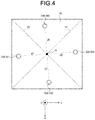
- the points at which the first feeding line 51, the second feeding line 52, the third feeding line 53, and the fourth feeding line 54 are connected to the radiation conductor 30 can be referred to as a feeding point 51A, a feeding point 52A, a feeding point 53A, and a feeding point 54A, respectively.
- the first feeding line 51, the second feeding line 52, the third feeding line 53, and the fourth feeding line 54 make contact with the radiation conductor 30 at mutually different positions.
- the ground conductor 40 has a plurality of openings 40a formed thereon.
- the first feeding line 51, the second feeding line 52, the third feeding line 53, and the fourth feeding line 54 are communicated to the outside via the openings 40a of the ground conductor 40.
- the first feeding line 51 to the fourth feeding line 54 can extend along the z direction.
- the first feeding line 51 is configured to contribute at least to supply, to the outside, the electrical signals generated at the time of resonance of the radiation conductor 30 in the y direction.
- the second feeding line 52 is configured to contribute at least to supply, to the outside, the electrical signals generated at the time of resonance of the radiation conductor 30 in the x direction.
- the third feeding line 53 is configured to contribute at least to supply, to the outside, the electrical signals generated at the time of resonance of the radiation conductor 30 in the y direction.
- the fourth feeding line 54 is configured to contribute at least to supply, to the outside, the electrical signals generated at the time of resonance of the radiation conductor 30 in the x direction.
- the pair of the first feeding line 51 and the third feeding line 53 and the pair of the second feeding line 52 and the fourth feeding line 54 are configured to excite the radiation conductor 30 in different directions.
- the first feeding line 51 and the third feeding line 53 are configured to excite the radiation conductor 30 in the y direction.
- the second feeding line 52 and the fourth feeding line 54 are configured to excite the radiation conductor 30 in the x direction.
- the antenna 10 enables reducing the excitation of the radiation conductor 30 in one direction during the excitation of the radiation conductor 30 in another direction.
- the first feeding line 51 and the third feeding line 53 are configured to excite the radiation conductor 30 using a differential voltage.
- the second feeding line 52 and the fourth feeding line 54 are configured to excite the radiation conductor 30 using a differential voltage.
- the antenna 10 enables achieving reduction in the fluctuation of the electric potential center at the time of excitation of the radiation conductor 30 from the center O of the radiation conductor 30.
- the position of the center O can be between the first feeding line 51 and the third feeding line 53.
- the third feeding line 53 is positioned on the substantially opposite side of the first feeding line 51 in the y direction.
- a first distance d1 between the first feeding line 51 and the center O is substantially equal to a third distance d3 between the third feeding line 53 and the center O.
- the position of the center O can be between the second feeding line 52 and the fourth feeding line 54.
- the fourth feeding line 54 is positioned on the substantially opposite side of the second feeding line 52 in the x direction.
- a second distance d2 between the second feeding line 52 and the center O is substantially equal to a fourth distance d4 between the fourth feeding line 54 and the center O.
- the second distance d2 can be substantially equal to the first distance d1.
- the second distance d2 can be different from the first distance d1.
- the first feeding line 51 and the second feeding line 52 can be symmetric across the first symmetrical axis S1.
- the third feeding line 53 and the fourth feeding line 54 can be symmetric across the first symmetrical axis S1.
- the feeding points 51A and 52A can be axisymmetric with respect to the first symmetrical axis S1 serving as the symmetrical axis.
- the feeding points 53A and 54A can be axisymmetric with respect to the first symmetrical axis S1 serving as the symmetrical axis.
- the first feeding line 51 and the fourth feeding line 54 can be symmetric across the second symmetrical axis S2.
- the second feeding line 52 and the third feeding line 53 can be symmetric across the second symmetrical axis S2.
- the feeding points 51A and 54A can be axisymmetric with respect to the second symmetrical axis S2 serving as the symmetrical axis.
- the feeding points 52A and 53A can be axisymmetric with respect to the second symmetrical axis S2 serving as the symmetrical axis.
- the direction connecting the first feeding line 51 and the third feeding line 53 is inclined with respect to the y direction. Because of the inclined arrangement of the first feeding line 51 and the third feeding line 53 with respect to the y direction, the first feeding line 51 and the third feeding line 53 become able to excite the radiation conductor 30 in the x direction too.
- the direction connecting the second feeding line 52 and the fourth feeding line 54 is inclined with respect to the x direction. Because of the inclined arrangement of the second feeding line 52 and the fourth feeding line 54 with respect to the x direction, the second feeding line 52 and the fourth feeding line 54 become able to excite the radiation conductor 30 in the y direction too.
- the pair of the first feeding line 51 and the third feeding line 53 and the pair of the second feeding line 52 and the fourth feeding line 54 enable excitation of the radiation conductor 30 in two excitation directions.
- the impedance components in the respective directions act on the feeding lines 50.
- the impedance at the time of input can be reduced.
- isolation of two polarization directions can be enhanced in the antenna 10.
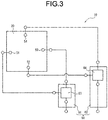
- the circuit board 60 includes a ground conductor 60A. As illustrated in FIG. 3 , the circuit board 60 includes a first feeding circuit 61 and a second feeding circuit 62. The circuit board 60 can include either the first feeding circuit 61 or the second feeding circuit 62.
- the ground conductor 60A is made of any electroconductive material.
- the ground conductor 60A can be made of the same material as the radiation conductor 30 and the ground conductor 40, or can be made of a different material from that of the radiation conductor 30 and the ground conductor 40. Some combination of the ground conductor 60A, the radiation conductor 30, and the ground conductor 40 can be made of the same material.
- the ground conductor 60A can be connected to a ground conductor 140.
- the ground conductor 60A can be integrated with the ground conductor 140.
- the first feeding circuit 61 is electrically connected to the first feeding line 51 and the third feeding line 53.
- the first feeding circuit 61 is configured to supply reversed-phase signals, which have mutually opposite phases, to the first feeding line 51 and the third feeding line 53.
- First feeding signals supplied to the first feeding line 51 are substantially opposite in phase to third feeding signals supplied to the third feeding line 53.
- the first feeding circuit 61 includes a first inverting circuit 63. Based on a single electrical signal input thereto, the first inverting circuit 63 is capable of outputting two electrical signals having mutually opposite phases.
- the first inverting circuit 63 can be a circuit for inverting the phase of a single input electrical signal in the resonance frequency band.
- the first inverting circuit 63 can be a circuit for outputting reversed-phase signals, which have substantially opposite phases to each other, from a single input electrical signal.
- the first inverting circuit 63 can be a balun, or a power divider circuit, or a delay line memory.
- the first inverting circuit 63 can include an inductance element connected to one of the first feeding line 51 and the third feeding line 53, and can include a capacitance element connected to the other of the first feeding line 51 and the third feeding line 53.
- the second feeding circuit 62 is configured to be electrically connected to the second feeding line 52 and the fourth feeding line 54.
- the second feeding circuit 62 is configured to supply reversed-phase signals, which have mutually opposite phases, to the second feeding line 52 and the fourth feeding line 54.
- Second feeding signals supplied to the second feeding line 52 are substantially opposite in phase to fourth feeding signals supplied to the fourth feeding line 54.
- the second feeding circuit 62 includes a second inverting circuit 64. Based on a single electrical signal input thereto, the second inverting circuit 64 is capable of outputting two electrical signals having mutually opposite phases.
- the second inverting circuit 64 can be a circuit for inverting the phase of a single input electrical signal in the resonance frequency band.
- the second inverting circuit 64 can be a circuit for outputting reversed-phase signals, which have substantially opposite phases to each other, from a single input electrical signal.
- the second inverting circuit 64 can be a balun, or a power divider circuit, or a delay line memory.
- the second inverting circuit 64 can include an inductance element connected to one of the second feeding line 52 and the fourth feeding line 54, and can include a capacitance element connected to the other feeding line.
- the antenna 10 In the antenna 10, electrical signals of opposite phases are fed to the first feeding line 51 and the third feeding line 53. In the antenna 10, when the radiation conductor 30 resonates along the y direction, there is a decrease in the potential variation in the vicinity of the center O of the radiation conductor 30.
- the antenna 10 is configured to resonate with the node in the vicinity of the center O. In the antenna 10, electrical signals of opposite phases are fed to the second feeding line 52 and the fourth feeding line 54. In the antenna 10, when the radiation conductor 30 resonates along the y direction, there is a decrease in the potential variation in the vicinity of the center O of the radiation conductor 30.
- FIG. 5 is a perspective view of an antenna 110 according to an embodiment.
- FIG. 6 is a cross-sectional view of the antenna 110 along L1-L1 line illustrated in FIG. 5 .
- FIG. 7 is an exploded perspective view of a portion of the antenna 110 illustrated in FIG. 5 .
- FIG. 8 is a block diagram of the antenna 110 illustrated in FIG. 5 .
- FIG. 9 is a planar view for explaining a configuration of a radiation conductor 130 illustrated in FIG. 5 .
- the antenna 110 includes a base 120, the radiation conductor 130, the ground conductor 140, first connecting conductors 155, second connecting conductors 156, third connecting conductors 157, and fourth connecting conductors 158.
- the antenna 110 includes feeding lines 150 and a circuit board 160.
- the radiation conductor 130, the ground conductor 140, and the feeding lines 150 function as an antenna element 111.
- the feeding lines 150 include a first feeding line 151, a second feeding line 152, a third feeding line 153, and a fourth feeding line 154.
- the numbers of the first connecting conductors 155 to the fourth connecting conductors 158 included in the antenna 110 illustrated in FIG. 5 are each two. However, the numbers of the first connecting conductor 155 to the fourth connecting conductor 158 included in the antenna 110 may be each one or three or more.
- the antenna element 111 is configured to oscillate at a predetermined resonance frequency.
- the antenna 110 can be configured to radiate electromagnetic waves.
- the antenna 110 can use at least one of one or more resonance frequency bands of the antenna element 111.
- the antenna 110 can radiate electromagnetic waves of the operating frequency.
- the wavelength of the operating frequency can be the operating wavelength that represents the wavelength of the electromagnetic waves in the operating frequency of the antenna 110.
- the antenna element 111 exhibits an artificial magnetic conductor character with respect to the electromagnetic waves of a predetermined frequency that are incident from the positive direction of the z axis on a surface substantially parallel to the x-y plane of the antenna element 111.
- the artificial magnetic conductor character implies the characteristics of a surface that has zero phase difference between the incident waves and the reflected waves in the operating frequency.
- a surface exhibiting the artificial magnetic conductor character has the phase difference between the incident waves and the reflected waves to be in the range from -90° to +90° in the operating frequency band.
- the operating frequency band includes the resonance frequency and the operating frequency that exhibit the artificial magnetic conductor character.
- the antenna element 111 exhibits the artificial magnetic conductor character, as illustrated in FIG. 5 , even when a ground conductor 165 (described later) of the circuit board 160 is positioned on the side of the negative direction of the z axis of the antenna 110, the radiation efficiency of the antenna 110 can be maintained.
- the base 120 is made of the same material or a similar material as the base 20 illustrated in FIG. 1 .
- the base 120 makes contact with the radiation conductor 130, the ground conductor 140, and the feeding lines 150.
- the base 120 can have the shape corresponding to the shape of the radiation conductor 130.
- the base 120 can have the shape of a substantially square prism.
- the base 120 has a top surface 121 and an under surface 122.
- the top surface 121 and the under surface 122 can be the top surface and the bottom surface, respectively, of the base 120 having the shape of a substantially square prism.
- the top surface 121 and the under surface 122 can be substantially parallel to the x-y plane.
- the top surface 121 and the under surface 122 can be substantially square in shape.
- top surface 121 and the under surface 122 that are substantially square in shape, one of the two diagonal lines runs along the x direction, while the other diagonal line runs along the y direction. As compared to the under surface 122, the top surface 121 is positioned more on the side of the positive direction of the z axis.
- the radiation conductor 130 is configured to function as a resonator.
- the radiation conductor 130 is made of the same material or a similar material as the radiation conductor 30 illustrated in FIG. 1 . As illustrated in FIG. 6 , the radiation conductor 130 can be positioned on the top surface 121 of the base 120.
- the radiation conductor 130 extends along the x-y plane.
- the radiation conductor 130 is configured to capacitively connect the connecting conductors from the first connecting conductor 155 to the fourth connecting conductor 158. In the x-y plane, the radiation conductor 130 is surrounded by the first connecting conductor 155 to the fourth connecting conductor 158.
- the radiation conductor 130 can be configured to resonate in the y direction when, for example, mutually reversed-phased electrical signals are supplied from the first feeding line 151 and the third feeding line 153.
- the first connecting conductor 155 is seen as an electrical conductor positioned on the side of the negative direction of the y axis
- the third connecting conductor 157 is seen as an electrical conductor positioned on the side of the positive direction of the y axis.
- the radiation conductor 130 resonates in the y direction; from the radiation conductor 130, the side in the positive direction the x axis is seen as magnetic conductor, and the side in the negative direction of the x axis is seen as magnetic conductor.
- the antenna 110 can be configured to exhibit the artificial magnetic conductor character with respect to the electromagnetic waves of a predetermined frequency that are incident from the positive direction of the z axis on the x-y plane included in the antenna 110.
- the radiation conductor 130 can be configured to resonate in the x direction when, for example, mutually reversed-phased electrical signals are supplied from the second feeding line 152 and the fourth feeding line 154.
- the second connecting conductor 156 is seen as an electrical conductor positioned on the side of the positive direction of the x axis
- the fourth connecting conductor 158 is seen as an electrical conductor positioned on the side of the negative direction of the x axis.
- the radiation conductor 130 resonates in the x direction; from the radiation conductor 130, the side on the positive direction of the y axis is seen as magnetic conductor, and the negative direction of the y axis is seen as magnetic conductor.
- the antenna 110 can be configured to exhibit the artificial magnetic conductor character with respect to the electromagnetic waves of a predetermined frequency that are incident from the positive direction of the z axis on the x-y plane included in the antenna 110.
- the radiation conductor 130 has a center O1.
- the center O1 is the center of the radiation conductor 130 in the x and y directions.
- the radiation conductor 130 can include a first symmetrical axis T1 that extends along the x-y plane.
- the first symmetrical axis T1 passes through the center O1 and extends in the direction intersecting with the x and y directions.
- the first symmetrical axis T1 can extend in the direction inclined by 45° from the positive direction of the y axis toward the negative direction of the x axis.
- the radiation conductor 130 can be half the size of the operating wavelength. For example, of the radiation conductor 130, the lengths in the x and y directions can be half of the operating wavelength.
- the radiation conductor 130 includes a first conductor 131, a second conductor 132, a third conductor 133, and a fourth conductor 134.
- the radiation conductor 130 can further include an internal conductor 135.
- the first conductor 131 to the fourth conductor 134, the internal conductor 135, the ground conductor 140, the first feeding line 151 to the fourth feeding line 154, and the first connecting conductor 155 to the fourth connecting conductor 158 can all be made of either the same material or different materials.
- Some combination of the first conductor 131 to the fourth conductor 134, the internal conductor 135, the ground conductor 140, the first feeding line 151 to the fourth feeding line 154, and the first connecting conductor 155 to the fourth connecting conductor 158 can be made of the same material.
- the first conductor 131 to the fourth conductor 134 can have the same shape, such as a substantially square shape.
- the two diagonal lines of the substantially square first conductor 131 and the two diagonal lines of the substantially square third conductor 133 run along the x and y directions.
- the length of that diagonal line of the first conductor 131 which runs along the y direction and the length of that diagonal line of the third conductor 133 which runs along the y direction can be about one-fourth of the operating wavelength.
- the two diagonal lines of the substantially square second conductor 132 and the two diagonal lines of the substantially square fourth conductor 134 run along the x and y directions.
- the length of that diagonal line of the second conductor 132 which runs along the x direction and the length of that diagonal line of the fourth conductor 134 which runs along the x direction can be about one-fourth of the operating wavelength.
- each of the first conductor 131 to the fourth conductor 134 can be exposed to the outside of the base 120. Some part of each of the first conductor 131 to the fourth conductor 134 can be positioned within the base 120. Each of the first conductor 131 to the fourth conductor 134 can be entirely positioned within the base 120.
- the first conductor 131 to the fourth conductor 134 extend along the top surface 121 of the base 120.
- the first conductor 131 to the fourth conductor 134 can be arranged in form of a square lattice on the top surface 121.
- the pair of the first conductor 131 and the fourth conductor 134 as well as the pair of the second conductor 132 and the third conductor 133 can be arranged along the first diagonal axis T1.
- the pair of the first conductor 131 and the second conductor 132 as well as the pair of the fourth conductor 134 and the third conductor 133 can be arranged along the second diagonal axis T2.
- the two diagonal directions run along the x and y directions. Of those two diagonal directions, the diagonal direction running along the y direction is referred to as a first diagonal direction. Of those two diagonal direction, the diagonal direction running along the x direction is referred to as a second diagonal direction.
- the first diagonal direction and the second diagonal direction can intersect at the center O1.
- the first conductor 131 to the fourth conductor 134 are positioned away from each other with predetermined spacing maintained therebetween.
- the first conductor 131 and the second conductor 132 are positioned away from each other with a spacing t1 maintained therebetween.
- the third conductor 133 and the fourth conductor 134 are positioned away from each other with the spacing t1 maintained therebetween.
- the first conductor 131 and the fourth conductor 134 are positioned away from each other with a spacing t2 maintained therebetween.
- the second conductor 132 and the third conductor 133 are positioned away from each other with the spacing t2 maintained therebetween.
- the internal conductor 135 faces the first conductor 131 to the fourth conductor 134 in the z direction. As compared to the first conductor 131 to the fourth conductor 134, the internal conductor 135 is positioned more in the negative direction of the z axis. As illustrated in FIG. 6 , the internal conductor 135 can be positioned within the base 120. However, when each of the first conductor 131 to the fourth conductor 134 is entirely positioned within the base 120, the internal conductor 135 can be positioned more in the positive direction of the z axis as compared to the first conductor 131 to the fourth conductor 134. In that case, at least some part of the internal conductor 135 can be exposed from the top surface 121 of the base 120.
- the internal conductor 135 is configured to be capacitively connected to each of the first conductor 131 to the fourth conductor 134.
- some part of the base 120 can be present between the internal conductor 135 and the first conductor 131 to the fourth conductor 134.
- the internal conductor 135 can be configured to be capacitively connected to each of the first conductor 131 to the fourth conductor 134.
- the surface integral in the x-y plane of the internal conductor 135 can be appropriately adjusted by taking into account the desired capacitive coupling strength between the internal conductor 135 and the first conductor 131 to the fourth conductor 134.
- the distances between the internal conductor 135 and the first conductor 131 to the fourth conductor 134 in the z direction can be appropriately adjusted by taking into account the desired capacitive coupling strength between the internal conductor 135 and the first conductor 131 to the fourth conductor 134.
- the internal conductor 135 can be substantially parallel to the x-y plane.
- the internal conductor 135 can be substantially square in shape.
- the center of the substantially square internal conductor 135 can substantially coincide with the center O1 in the first conductor 131 to the fourth conductor 134.
- one diagonal line can run along the first diagonal direction and the other diagonal line can run along the second diagonal direction.
- the ground conductor 140 is made of the same material or a similar material as the ground conductor 40 illustrated in FIG. 2 .
- the ground conductor 140 is configured to function as the ground conductor of the antenna element 111.
- the ground conductor 140 can be configured to be connected to the ground conductor 165 (described later) of the circuit board 160. In that case, the ground conductor 140 can be integrated with the ground conductor 165 of the circuit board 160.
- the ground conductor 140 can be a plate conductor.
- the ground conductor 140 is positioned on the under surface 122 of the base 120.
- the ground conductor 140 extends along the x-y plane. In the z direction, the ground conductor 140 faces the radiation conductor 130.
- the base 120 is present between the ground conductor 140 and the radiation conductor 130.
- the ground conductor 140 can have the shape corresponding to the shape of the radiation conductor 130. In the present embodiment, the ground conductor 140 is substantially square in shape corresponding to the substantially square shape of the radiation conductor 130. However, the ground conductor 140 can have an arbitrary shape according to the radiation conductor 130.
- the ground conductor 140 has openings 141, 142, 143, and 144 formed thereon. The positions of the openings 141 to 144 on the x-y plane can be appropriately adjusted according to the positions of the first feeding line 151 to the fourth feeding line 154, respectively, in the x-y plane.
- the feeding lines 150 are made of the same material or a similar material as the feeding lines 50 illustrated in FIG. 1 .
- the feeding lines 150 can be through-hole conductors or via conductors.
- the feeding lines 150 are configured to be able to supply electrical signals from the antenna element 111 to the circuit board 160 present on the outside.
- the first feeding line 151 to the fourth feeding line 154 make contact with the radiation conductor 130 at mutually different positions.
- the first feeding line 151 is configured to be electrically connected to the first conductor 131.
- the second feeding line 152 is configured to be electrically connected to the second conductor 132.
- the third feeding line 153 is configured to be electrically connected to the third conductor 133.
- the fourth feeding line 154 is configured to be electrically connected to the fourth conductor 134.
- the first feeding line 151 to the fourth feeding line 154 can be configured to be magnetically connected to the first conductor 131 to the fourth conductor 134, respectively.
- the points at which the first feeding line 151 to the fourth feeding line 154 are connected to the first conductor 131 to the fourth conductor 134, respectively, can be referred to as a feeding point 151A, a feeding point 152A, a feeding point 153A, and a feeding point 154A, respectively.
- the first feeding line 151 to the fourth feeding line 154 are communicated to the outside via the openings 141 to 144, respectively, of the ground conductor 140.
- the first feeding line 151 to the fourth feeding line 154 can extend along the z direction.
- the first feeding line 151 and the third feeding line 153 are configured to at least contribute in supplying, to the outside, the electrical signals generated at the time of resonance of the radiation conductor 130 in the y direction.
- the second feeding line 152 and the fourth feeding line 154 are configured to at least contribute in supplying, to the outside, the electrical signals generated at the time of resonance of the radiation conductor 130 in the x direction.
- the pair of the first feeding line 151 and the third feeding line 153 and the pair of the second feeding line 152 and the fourth feeding line 154 are configured to excite the radiation conductor 130 in different directions.
- the first feeding line 151 and the third feeding line 153 are configured to excite the radiation conductor 130 in the y direction.
- the second feeding line 152 and the fourth feeding line 154 are configured to excite the radiation conductor 130 in the x direction.
- the antenna 110 enables achieving reduction in the occurrence of a situation in which, at the time of exciting the radiation conductor 130 in one direction, it gets excited in another direction.
- the first feeding line 151 and the third feeding line 153 are configured to excite the radiation conductor 130 using a differential voltage.
- the second feeding line 152 and the fourth feeding line 154 are configured to excite the radiation conductor 130 using a differential voltage.
- the antenna 110 enables achieving reduction in the fluctuation of the electric potential center at the time of excitation of the radiation conductor 130 from the center O of the radiation conductor 130.
- the center O1 of the radiation conductor 130 is positioned between the first feeding line 151 and the third feeding line 153.
- a first distance D1 between the first feeding line 151 and the center O1 is substantially equal to a third distance D3 between the third feeding line 153 and the center O1.
- the center O1 of the radiation conductor 130 is positioned between the second feeding line 152 and the fourth feeding line 154.
- a second distance D2 between the second feeding line 152 and the center O1 is substantially equal to a fourth distance D4 between the fourth feeding line 154 and the center O1.
- the second distance D2 is substantially equal to the first distance D1.
- the second distance D2 can be different from the first distance D1.
- the first feeding line 151 and the second feeding line 152 can be symmetric across the first symmetrical axis T1.
- the third feeding line 153 and the fourth feeding line 154 can be symmetric across the first symmetrical axis T1.
- the feeding points 151A and 152A as well as the feeding points 153A and 154A can be axisymmetric with respect to the first symmetrical axis T1.
- the first feeding line 151 and the fourth feeding line 154 can be symmetric across the second symmetrical axis T2.
- the second feeding line 152 and the third feeding line 153 can be symmetric across the second symmetrical axis T2.
- the feeding points 151A and 154A as well as the feeding points 152A and 153A can be axisymmetric with respect to the second symmetrical axis T2.
- the direction connecting the first feeding line 151 and the third feeding line 153 runs along the y direction.
- the direction connecting the first feeding line 151 and the third feeding line 153 runs along the first diagonal direction.
- the direction connecting the second feeding line 152 and the fourth feeding line 154 runs along the x direction.
- the direction connecting the second feeding line 152 and the fourth feeding line 154 runs along the second diagonal direction.
- the direction connecting the first feeding line 151 and the third feeding line 153 can be inclined with respect to the first diagonal direction.
- the direction connecting the second feeding line 152 and the fourth feeding line 154 can be inclined with respect to the second diagonal direction.
- the circuit board 160 includes a first feeding circuit 61A and a second feeding circuit 62A. As illustrated in FIG. 6 , the circuit board 160 includes the ground conductor 165.
- the first feeding circuit 61A is configured to be electrically connected to the first feeding line 151 and the third feeding line 153.
- the first feeding circuit 61A includes the first inverting circuit 63, first wiring 161, and third wiring 163.
- the first inverting circuit 63 can include an inductance element connected to one of the first feeding line 151 and the third feeding line 153, and can include a capacitance element connected to the other feeding line.
- the first feeding circuit 61A is configured to supply reversed-phase signals, which have substantially opposite phases to each other, to the first feeding line 151 and the third feeding line 153. In the antenna 110, electrical signals having opposite phases are supplied to the first feeding line 151 and the third feeding line 153.
- the antenna 110 when the radiation conductor 130 resonates along the y direction, there is a decrease in the potential variation of the first conductor 131 to the fourth conductor 134 in the vicinity of the center O1.
- the antenna 110 is configured to resonate with a node in the vicinity of the center O1.
- the second feeding circuit 62A is configured to be electrically connected to the second feeding line 152 and the fourth feeding line 154.
- the second feeding circuit 62A includes the second inverting circuit 64, second wiring 162, and fourth wiring 164.
- the second inverting circuit 64 can include an inductance element connected to one of the second feeding line 152 and the fourth feeding line 154, and can include a capacitance element connected to the other feeding line.
- the second feeding circuit 62A is configured to supply reversed-phase signals, which have substantially opposite phases to each other, to the second feeding line 152 and the fourth feeding line 154. In the antenna 110, electrical signals having opposite phases are supplied to the second feeding line 152 and the fourth feeding line 154.
- the antenna 110 when the radiation conductor 130 resonates along the x direction, there is a decrease in the potential variation of the first conductor 131 to the fourth conductor 134 in the vicinity of the center O1.
- the antenna 110 is configured to resonate with a node in the vicinity of the center O1.
- the first wiring 161 to the fourth wiring 164 are made of an arbitrary electroconductive material. As described later, the first wiring 161 to the fourth wiring 164 are formed as wiring patterns.
- the first wiring 161 is configured to electrically connect the first inverting circuit 63 and the first feeding line 151.
- the second wiring 162 is configured to electrically connect the second inverting circuit 64 and the second feeding line 152.
- the third wiring 163 is configured to electrically connect the first inverting circuit 63 and the third feeding line 153.
- the fourth wiring 164 is configured to electrically connect the second inverting circuit 64 and the fourth feeding line 154.
- the wiring length and the width of the first wiring 161 can be substantially equal to the wiring length and the width of the third wiring 163.
- the impedance of the first wiring 161 can become substantially equal to the impedance of the third wiring 163.
- the wiring length and the width of the second wiring 162 can be substantially equal to the wiring length and the width of the fourth wiring 164.
- the impedance of the second wiring 162 can become substantially equal to the impedance of the fourth wiring 164.
- the ground conductor 165 can be made of an arbitrary electroconductive material.
- the ground conductor 165 can represent a conductor layer.
- the surface positioned on the side of the positive direction of the z axis has the ground conductor 165 installed thereon.
- FIG. 10 is a perspective view of an antenna 210 according to an embodiment.
- FIG. 11 is an exploded perspective view of a portion of the antenna 210 illustrated in FIG. 10 .
- the following explanation is given about the major differences between the antenna 210 illustrated in FIG. 10 and the antenna 110 illustrated in FIG. 5 .
- the antenna 210 includes the base 120, a radiation conductor 230, the ground conductor 140, and the first connecting conductor 155 to the fourth connecting conductor 158.
- the antenna 210 includes the first feeding line 151, the second feeding line 152, the third feeding line 153, the fourth feeding line 154, and the circuit board 160.
- the radiation conductor 230, the ground conductor 140, the first connecting conductor 155 to the fourth connecting conductor 158, and the feeding lines 150 are configured to function as an antenna element 211.
- the radiation conductor 230 includes the first conductor 131 to the fourth conductor 134 and an internal conductor 235.
- the internal conductor 235 can be made of the same material or a similar material as the internal conductor 135 illustrated in FIG. 7 .
- the internal conductor 235 includes a first branch portion 235a, a second branch portion 235b, a first internal conductor 236, a second internal conductor 237, a third internal conductor 238, and a fourth internal conductor 239.
- the first branch portion 235a, the second branch portion 235b, the first internal conductor 236, the second internal conductor 237, the third internal conductor 238, and the fourth internal conductor 239 can all be made of either the same material or different materials.
- the first internal conductor 236 faces the first conductor 131 in the z direction.
- the first internal conductor 236 is positioned away from the first conductor 131 in the z direction.
- the entire first internal conductor 236 can overlap with the first conductor 131.
- the surface integral in the x-y plane of the first internal conductor 236 can be smaller than the surface integral in the x-y plane of the first conductor 131. Since some part of the base 120 is present between the first internal conductor 236 and the first conductor 131, the first internal conductor 236 is configured to be capacitively connected to the first conductor 131.
- the position of the first internal conductor 236 in the x-y plane can be appropriately adjusted according to the position of the first conductor 131 in the x-y plane.
- the second internal conductor 237 faces the second conductor 132 in the z direction.
- the second internal conductor 237 is positioned away from the second conductor 132 in the z direction.
- the entire second internal conductor 237 can overlap with the second conductor 132.
- the surface integral in the x-y plane of the second internal conductor 237 can be smaller than the surface integral in the x-y plane of the second conductor 132. Since some part of the base 120 is present between the second internal conductor 237 and the second conductor 132, the second internal conductor 237 is configured to be capacitively connected to the second conductor 132.
- the position of the second internal conductor 237 in the x-y plane can be appropriately adjusted according to the position of the second conductor 132 in the x-y plane.
- the third internal conductor 238 faces the third conductor 133 in the z direction.
- the third internal conductor 238 is positioned away from the third conductor 133 in the z direction.
- the entire third internal conductor 238 can overlap with the third conductor 133.
- the surface integral in the x-y plane of the third internal conductor 238 can be smaller than the surface integral in the x-y plane of the third conductor 133. Since some part of the base 120 is present between the third internal conductor 238 and the third conductor 133, the third internal conductor 238 is configured to be capacitively connected to the third conductor 133.
- the position of the third internal conductor 238 in the x-y plane can be appropriately adjusted according to the position of the third conductor 133 in the x-y plane.
- the fourth internal conductor 239 faces the fourth conductor 134 in the z direction.
- the fourth internal conductor 239 is positioned away from the fourth conductor 134 in the z direction.
- the entire fourth internal conductor 239 can overlap with the fourth conductor 134.
- the surface integral in the x-y plane of the fourth internal conductor 239 can be smaller than the surface integral in the x-y plane of the fourth conductor 134. Since some part of the base 120 is present between the fourth internal conductor 239 and the fourth conductor 134, the fourth internal conductor 239 is configured to be capacitively connected to the fourth conductor 134.
- the position of the fourth internal conductor 239 in the x-y plane can be appropriately adjusted according to the position of the fourth conductor 134 in the x-y plane.
- Each of the first internal conductor 236 to the fourth internal conductor 239 can have the shape of a flat plate.
- Each of the first internal conductor 236 to the fourth internal conductor 239 can be substantially square in shape.
- the first internal conductor 236 to the fourth internal conductor 239 are not limited to have a square shape.
- the first internal conductor 236 to the fourth internal conductor 239 can be circular or elliptical in shape.
- the first internal conductor 236 to the fourth internal conductor 239 can all have either the same shape or different shapes.
- the first branch portion 235a is configured to electrically connect the first internal conductor 236 and the third internal conductor 238.
- One end of the first branch portion 235a is configured to be electrically connected to one of the four corners of the first internal conductor 236.
- the other end of the first branch portion 235a is configured to be electrically connected to one of the four corners of the third internal conductor 238.
- the first branch portion 235a can extend along the direction connecting the first feeding line 151 and the third feeding line 153.
- the first branch portion 235a can extend along the y direction.
- the width of the first branch portion 235a in the x direction can be thin enough to be able to maintain the mechanical connection or the electrical connection between the first internal conductor 236 and the third internal conductor 238.
- the second branch portion 235b is configured to electrically connect the second internal conductor 237 and the fourth internal conductor 239.
- One end of the second branch portion 235b is configured to be electrically connected to one of the four corners of the second internal conductor 237.
- the other end of the second branch portion 235b is configured to be electrically connected to one of the four corners of the fourth internal conductor 239.
- the second branch portion 235b can extend along the direction connecting the second feeding line 152 and the fourth feeding line 154.
- the second branch portion 235b can extend along the x direction.
- the width of the second branch portion 235b in the y direction can be thin enough to be able to maintain the mechanical connection or the electrical connection between the second internal conductor 237 and the fourth internal conductor 239.
- the first branch portion 235a and the second branch portion 235b can intersect with each other in the vicinity of the center O1 of the radiation conductor 230.
- the first branch portion 235a and the second branch portion 235b can have some common part in the vicinity of the center O1.
- the width of the first branch portion 235a in the x direction can be either same as or different from the width of the second branch portion 235b in the y direction.
- the capacitive coupling of the first internal conductor 236 to the fourth internal conductor 239 with the first conductor 131 to the fourth conductor 134, respectively, can be greater than the capacitive coupling of the first branch portion 235a and the second branch portion 235b with the first conductor 131 to the fourth conductor 134.
- the capacitive coupling of the first internal conductor 236 to the fourth internal conductor 239 with the first conductor 131 to the fourth conductor 134, respectively can be dominant.
- the positions of the first conductor 131 to the fourth conductor 134 in the x-y plane may be misaligned from the position of the internal conductor 235 in the x-y plane. Even if such misalignment occurs, there can be a decrease in the amount of misalignment of the first internal conductor 236 to the fourth internal conductor 239 with respect to the first conductor 131 to the fourth conductor 134, respectively.
- the decrease in that amount of misalignment enables achieving reduction in the probability that the capacitive coupling of the internal conductor 235 with the first conductor 131 to the fourth conductor 134 deviates from the design value. With such a configuration, in the antenna 210, the variability in the capacitive coupling of the internal conductor 235 with the first conductor 131 to the fourth conductor 134 can be reduced.
- FIG. 12 is a perspective view of an antenna 310 according to an embodiment.
- FIG. 13 is an exploded perspective view of a portion of a circuit board 360 illustrated in FIG. 12 .
- FIG. 14 is a cross-sectional view of the circuit board 360 along L2-L2 line illustrated in FIG. 13 .
- FIG. 15 is a planar view for explaining a configuration of a radiation conductor 330 illustrated in FIG. 12 . The following explanation is given about the major differences between the antenna 310 illustrated in FIG. 12 and the antenna 110 illustrated in FIG. 5 .
- the antenna 310 includes the base 120, the radiation conductor 330, the ground conductor 140, and the first connecting conductor 155 to the fourth connecting conductor 158.
- the antenna 310 includes the first feeding line 151, the second feeding line 152, the third feeding line 153, the fourth feeding line 154, and the circuit board 360 (a multi-layer wiring substrate).
- the radiation conductor 330, the ground conductor 140, the first connecting conductor 155 to the fourth connecting conductor 158, and the feeding lines 150 are configured to function as an antenna element 311.
- the radiation conductor 330 includes the first conductor 131, the second conductor 132, the third conductor 133, and the fourth conductor 134. As illustrated in FIG. 15 , the radiation conductor 330 includes the internal conductor 135. However, in place of including the internal conductor 135, the radiation conductor 330 can include the internal conductor 235 illustrated in FIG. 11 .
- the first conductor 131 to the fourth conductor 134 are arranged in form of a square lattice on the top surface 121.
- the first diagonal direction is inclined with respect to the y direction.
- the first diagonal direction can be inclined with respect to the direction connecting the first feeding line 151 and the third feeding line 153, e.g., with respect to the y direction.
- the first feeding line 151 and the third feeding line 153 can excite the radiation conductor 330 in the x direction too.
- the second diagonal direction is inclined with respect to the x direction.
- the second diagonal direction can be inclined with respect to the direction connecting the second feeding line 152 and the fourth feeding line 154, e.g., with respect to the x direction.
- the second feeding line 152 and the fourth feeding line 154 can excite the radiation conductor 330 in the y direction too.
- the pair of the first feeding line 151 and the third feeding line 153 and the pair of the second feeding line 152 and the fourth feeding line 154 enable excitation of the radiation conductor 330 in two excitation directions.
- the impedance component in each direction acts on the feeding lines 150.
- the antenna 310 by cancelling out the impedance component in each direction, the impedance at the time of input can be reduced.
- isolation in two polarization directions can be enhanced in the antenna 310.
- the angle of inclination of the first diagonal direction with respect to the y direction and the angle of inclination of the second diagonal direction with respect to the x direction can be appropriately adjusted by taking into account the desired gain of the antenna 310.
- one diagonal line can run along the first diagonal direction.
- one diagonal line can be inclined with respect to the y direction in the same manner as or in a similar manner to the first diagonal direction.
- the other diagonal line can run along the second diagonal direction.
- the other diagonal line can be inclined with respect to the x direction in the same manner as or in a similar manner to the second diagonal direction.
- the circuit board 360 has a structure in which the layers are laminated along the z direction.
- the lamination direction of the circuit board 360 can correspond to the z direction.
- the layer positioned on the opposite side of the antenna 310 is called the bottom layer.
- the layer positioned on the side of the antenna 310 is called the top layer.
- the circuit board 360 includes a first feeding circuit 61B and a second feeding circuit 62B.
- the first feeding circuit 61B includes a first inverting circuit 63A.
- the second feeding circuit 62B includes a second inverting circuit 64A.
- the first inverting circuit 63A and the second inverting circuit 64A are baluns.
- the first inverting circuit 63A can be positioned away from the center O1 of the radiation conductor 330 along the x direction. The distance from the center O1 of the radiation conductor 330 to the first inverting circuit 63A is referred to as a distance D5.
- the second inverting circuit 64A can be positioned away from the center O1 of the radiation conductor 330 along the y direction.
- the distance from the center O1 of the radiation conductor 330 to the second inverting circuit 64A is referred to as a distance D6.
- the distance D5 can be different from the distance D6.
- the circuit board 360 includes a first wiring pattern 361 and a dielectric layer 361A; a second wiring pattern 362 and a dielectric layer 362A; a third wiring pattern 363 and a dielectric layer 363A; and a fourth wiring pattern 364 and a dielectric layer 364A.
- the circuit board 360 includes a ground conductor layer 365, conductor layers 366 and 367, a first layer 368, and a second layer 369.
- the first wiring pattern 361 to the fourth wiring pattern 364 can be same as the first wiring 161 to the fourth wiring 164, respectively, illustrated in FIG. 8 .
- the first wiring pattern 361 is configured to electrically connect the first inverting circuit 63A and the first feeding line 151.
- the second wiring pattern 362 is configured to electrically connect the second inverting circuit 64A and the second feeding line 152.
- the third wiring pattern 363 is configured to electrically connect the first inverting circuit 63A and the third feeding line 153.
- the fourth wiring pattern 364 is configured to electrically connect the second inverting circuit 64A and the fourth feeding line 154.
- the points at which the first feeding line 151 to the fourth feeding line 154 are connected to the first wiring pattern 361 to the fourth wiring pattern 364, respectively, are referred to as connecting points 151B, 152B, 153B, and 154B, respectively.
- the first wiring pattern 361 and the third wiring pattern 363 are positioned in the first layer 368 illustrated in FIG. 14 .
- the first wiring pattern 361 and the third wiring pattern 363 can extend along the x-y plane.
- the first wiring pattern 361 and the third wiring pattern 363 can be axisymmetric with respect to the symmetrical axis along the direction connecting the center O1 of the radiation conductor 330 and the first inverting circuit 63A. Because of the axisymmetric nature of the first wiring pattern 361 and the third wiring pattern 363, the width and the wiring length of the first wiring pattern 361 can be equal to the width and the wiring length of the third wiring pattern 363.
- the wiring lengths of the first wiring pattern 361 and the third wiring pattern 363 can increase and decrease in proportion to the distance D5 illustrated in FIG. 15 .
- the second wiring pattern 362 and the fourth wiring pattern 364 are positioned in the second layer 369 illustrated in FIG. 14 .
- the second wiring pattern 362 and the fourth wiring pattern 364 can extend along the x-y plane.
- the second wiring pattern 362 and the fourth wiring pattern 364 can be axisymmetric with respect to the symmetrical axis along the direction connecting the center O1 of the radiation conductor 330 and the second inverting circuit 64A. Because of the axisymmetric nature of the second wiring pattern 362 and the fourth wiring pattern 364, the width and the wiring length of the second wiring pattern 362 can be equal to the width and the wiring length of the fourth wiring pattern 364.
- the wiring lengths of the second wiring pattern 362 and the fourth wiring pattern 364 can increase and decrease in proportion to the distance D6 illustrated in FIG. 15 .
- the wiring lengths of the first wiring pattern 361 and the third wiring pattern 363 either can be substantially equal to or can be different from the wiring lengths of the second wiring pattern 362 and the fourth wiring pattern 364. If the distances D5 and D6 illustrated in FIG. 15 are different, then the wiring lengths of the first wiring pattern 361 and the third wiring pattern 363 can be different from the wiring lengths of the second wiring pattern 362 and the fourth wiring pattern 364. In the present embodiment, by appropriately adjusting the distances D5 and D6, the relationship of the wiring lengths of the first wiring pattern 361 and the third wiring pattern 363 with the wiring lengths of the second wiring pattern 362 and the fourth wiring pattern 364 can be adjusted.
- the dielectric layers 361A to 364A are made of an arbitrary electroconductive material.
- the dielectric layers 361A to 364A surround the first wiring pattern 361 to the fourth wiring pattern 364, respectively.
- the dielectric layers 361A to 364A can have the shapes dependent on the shapes of the first wiring pattern 361 to the fourth wiring pattern 364, respectively.
- the dielectric layers 361A and 363A are positioned in the first layer 368.
- the dielectric layers 362A and 364A are positioned in the second layer 369.
- the ground conductor layer 365 can be made of the same or similar material as the ground conductor 165 illustrated in FIG. 6 .
- the ground conductor layer 365 can extend along the x-y plane.
- the ground conductor layer 365 can be the topmost layer of the circuit board 360.
- the ground conductor layer 365 faces the ground conductor 140 of the antenna 310.
- the ground conductor layer 365 can be integrated with the ground conductor 140 of the antenna 310.
- the conductor layers 366 and 367 can be made of the same or similar material as the ground conductor 165 illustrated in FIG. 6 .
- the conductor layer 366 is the lower layer of the first layer 366.
- the conductor layer 367 is positioned between the first layer 368 and the second layer 369.
- the conductor layers 366 and 367 can extend along the x-y plane.
- the conductor layers 366 and 367 can be configured to be electrically connected to the ground conductor layer 365 through via holes.
- the conductor layers 366 and 377 are configured to shield the first wiring pattern 361 and the third wiring pattern 363 in the z direction.
- the conductor layer 367 and the ground conductor layer 365 are configured to shield the second wiring pattern 362 and the fourth wiring pattern 364 in the z direction.
- the first layer 368 is a lower layer than the second layer 369. In the lamination direction of the circuit board 360, for example, in the z direction; the first layer 368 is positioned farther from the radiation conductor 330 than the second layer 369.
- the first layer 368 includes the first wiring pattern 361 and the dielectric layer 361A; the third wiring pattern 363 and the dielectric layer 363A; and a conductor layer 368A.
- the conductor layer 368A can be made of the same or similar material as the ground conductor 165 illustrated in FIG. 6 .
- the conductor layer 368A can be configured to be electrically connected, using via holes, to the conductor layer 366, which is the bottom layer of the first layer 368, and to the conductor layer 367, which is the top layer of the first layer 368.
- the conductor layer 368A can be configured to fill the places excluding the dielectric layers 361A and 363A.
- the conductor layer 368A is configured to shield the first wiring pattern 361 and the third wiring pattern 363 in the x and y directions.
- the second layer 369 includes the second wiring pattern 362 and the dielectric layer 362A; the fourth wiring pattern 364 and the dielectric layer 364A; and a conductor layer 369A.
- the conductor layer 369A can be made of the same or similar material as the ground conductor 165 illustrated in FIG. 6 .
- the conductor layer 369A can be configured to be electrically connected, using via holes, to the ground conductor layer 365, which is the top layer of the second layer 369, and to the conductor layer 367, which is the bottom layer of the second layer 369.
- the conductor layer 369A can be configured to fill the places excluding the dielectric layers 362A and 364A.
- the conductor layer 369A is configured to shield the second wiring pattern 362 and the fourth wiring pattern 364 in the x and y directions.
- the first feeding line 151 and the third feeding line 153 are configured to be electrically connected to the first wiring pattern 361 and the third wiring pattern 363, respectively.
- the first wiring pattern 361 and the third wiring pattern 363 are positioned in the same first layer 368. Since the first wiring pattern 361 and the third wiring pattern 363 are positioned in the same first layer 368, the positions of the connecting points 151B and 153B in the z direction can be substantial same. Because of the substantially same positions of the connecting points 151B and 153B in the z direction, the positions of the feeding points 151A and 153A in the z direction can be substantially equal. Consequently, the length of the first feeding line 151 in the z direction can be substantially equal to the length of the third feeding line 153 in the z direction.
- the second feeding line 152 and the fourth feeding line 154 are configured to be electrically connected to the second wiring pattern 362 and the fourth wiring pattern 364, respectively.
- the second wiring pattern 362 and the fourth wiring pattern 364 are positioned in the same second layer 369. Since the second wiring pattern 362 and the fourth wiring pattern 364 are positioned in the same second layer 369, the positions of the connecting points 152B and 154B in the z direction can be substantial same. Because of the substantially same positions of the connecting points 152B and 154B in the z direction, the positions of the feeding points 152A and 154A in the z direction can be substantially equal. Consequently, the length of the second feeding line 152 in the z direction can be substantially equal to the length of the fourth feeding line 154 in the z direction.
- the first layer 368 is a lower layer than the second layer 369. Because the first layer 368 is a lower layer than the second layer 369, the connecting points 151B and 153B positioned on the first layer 368 are positioned more on the side of the negative direction of the z axis than the connecting points 152B and 154B positioned on the second layer. As illustrated in FIG. 13 , the positions of the feeding points 151A, 152A, 153A, and 154A in the z direction can be substantially same. Hence, the lengths of the first feeding line 151 and the third feeding line 153 in the z direction can be longer than the lengths of the second feeding line 152 and the fourth feeding line 154 in the z direction. The resistance values of the first feeding line 151 and the third feeding line 153 can be higher than the resistance values of the second feeding line 152 and the fourth feeding line 154.
- the distance D6 can be greater than the distance D5 as illustrated in FIG. 15 . Since the distance D6 is greater than the distance D5, the wiring lengths of the second wiring pattern 362 and the fourth wiring pattern 364 can be greater than the wiring lengths of the first wiring pattern 361 and the third wiring pattern 363. The resistance values of the second wiring pattern 362 and the fourth wiring pattern 364 can be greater than the resistance values of the first wiring pattern 361 and the third wiring pattern 363.
- the resistance value from the first inverting circuit 63A to each of the feeding points 151A and 153A can be substantially equal to the resistance value from the second inverting circuit 64A to each of the feeding points 152A and 154A.
- the characteristics of the baluns of the first inverting circuit 63A and the second inverting circuit 64A may vary within the acceptable error range. In that case, the phase difference between two electrical signals output from the first inverting circuit 63A as well as the phase difference between two electrical signals output from the second inverting circuit 64A may shift from 180°.
- the degree of interference among the first wiring pattern 361 to the fourth wiring pattern 364 may change as compared to the case in which the phase difference of such two electrical signals has not shifted from 180°.
- the distances D5 and D6 can be appropriately adjusted by taking into account the desired gain of the antenna 310 in the desired frequency band.
- the direction connecting the center O1 of the radiation direction 330 and the first inverting circuit 63A can be inclined with respect to the x direction.
- the direction connecting the center O1 of the radiation direction 330 and the first inverting circuit 63A can be ensured to be inclined with respect to the x direction in such a way that the electrical signals at the feeding point 151A have the phase difference of 180° with respect to the electrical signals at the feeding point 153A.
- the direction connecting the center O1 of the radiation direction 330 and the second inverting circuit 64A can be inclined with respect to the y direction.
- the direction connecting the center O1 of the radiation direction 330 and the second inverting circuit 64A can be ensured to be inclined with respect to the y direction in such a way that the electrical signals at the feeding point 152A have the phase difference of 180° with respect to the electrical signals at the feeding point 154A.
- FIG. 16 is a planar diagram illustrating an array antenna 12 according to an embodiment.
- the array antenna 12 includes a plurality of antenna elements 11. However, instead of including the antenna elements 11, the array antenna 12 can include the antenna elements 111 illustrated in FIG. 5 , or the antenna elements 211 illustrated in FIG. 10 , or the antenna elements 311 illustrated in FIG. 12 .
- the antenna elements 11 can be lined along the y direction.
- the antenna elements 11 can be arranged in the y direction.
- the antenna elements 11 can be lined along the x direction.
- the antenna elements 11 can be arranged in the x direction.
- the array antenna 12 includes at least one circuit board 60.
- the circuit board 60 includes at least one first feeding circuit 61 and at least one second feeding circuit 62.
- the array antenna 12 includes at least one first feeding circuit 61 and at least one second feeding circuit 62.
- the first feeding circuit 61 can be configured to be connected to one or more antenna elements 11. At the time of feeding power to a plurality of antenna elements 11, the first feeding circuit 61 can be configured to supply the same signal to all antenna elements 11. At the time of feeding power to a plurality of antenna elements 11, the first feeding circuit 61 can be configured to supply the same signal to the first feeding line 51 of each antenna element 11. At the time of feeding power to a plurality of antenna elements 11, the first feeding circuit 61 can be configured to supply a signal having a different phase to the first feeding line 51 of each antenna element 11. At the time of feeding power to a plurality of antenna elements 11, the first feeding circuit 61 can be configured to supply the same signal to the third feeding line 53 of each antenna element 11. At the time of feeding power to a plurality of antenna elements 11, the first feeding circuit 61 can be configured to supply a signal having a different phase to the third feeding line 53 of each antenna element 11.
- the second feeding circuit 62 can be configured to be connected to one or more antenna elements 11. At the time of feeding power to a plurality of antenna elements 11, the second feeding circuit 62 can be configured to supply the same signal to all antenna elements 11. At the time of feeding power to a plurality of antenna elements 11, the second feeding circuit 62 can be configured to supply the same signal to the second feeding line 52 of each antenna element 11. At the time of feeding power to a plurality of antenna elements 11, the second feeding circuit 62 can be configured to supply a signal having a different phase to the second feeding line 52 of each antenna element 11. At the time of feeding power to a plurality of antenna elements 11, the second feeding circuit 62 can be configured to supply the same signal to the fourth feeding line 54 of each antenna element 11. At the time of feeding power to a plurality of antenna elements 11, the second feeding circuit 62 can be configured to supply a signal having a different phase to the fourth feeding line 54 of each antenna element 11.
- FIG. 17 is a planar view of a radio communication module 70 according to an embodiment.
- the radio communication module 70 includes a driving circuit 71, which is configured to drive the antenna element 11.
- the driving circuit 71 can be configured to drive the antenna element 111 illustrated in FIG. 5 , or to drive the antenna element 211 illustrated in FIG. 10 , or to drive the antenna element 311 illustrated in FIG. 12 .
- the driving circuit 71 is configured to be connected, directly or indirectly, to the first feeding circuit 61 and the second feeding circuit 62.
- the driving circuit 71 can be configured to feed transmission signals to at least one of the first feeding circuit 61 and the second feeding circuit 62.
- the driving circuit 71 can be configured to receive the feed of reception signals from at least one of the first feeding circuit 61 and the second feeding circuit 62.
- FIG. 18 is a planar view of a radio communication device 80 according to an embodiment.
- the radio communication device 80 can include the radio communication module 70, a sensor 81, and a battery 82.
- the sensor 81 performs sensing operations.
- the battery 82 is configured to supply electric power to the parts of the radio communication device 80.
- the driving circuit 71 can be configured to perform driving when supplied with electrical power from the battery 82.
- FIG. 19 is a planar view of a radio communication system 90 according to an embodiment.
- the radio communication system 90 includes the radio communication device 80 and a second radio communication device 91.
- the second radio communication device 91 is configured to perform radio communication with the radio communication device 80.
- the antenna 10, 110, 210, 310; the array antenna 12; the radio communication module 70; and the radio communication device 80 of a new type can be provided.
- the configuration according to the present disclosure is not limited to embodiments described above, and it is possible to have a number of modifications and variations.
- the functions included in the constituent elements can be rearranged without causing any logical contradiction.
- a plurality of constituent elements can be combined into a single constituent elements, or constituent elements can be divided.
- a patch-type antenna is used as the antenna element 11.
- the antenna element 11 is not limited to a patch-type antenna. Some other type of antenna can be used as the antenna element 11.
- a plurality of antenna elements 11 can be lined with the same orientation.
- two neighboring antenna elements 11 can have different orientations.
- the antenna element 11 is excited in one direction.
- the terms “first”, “second”, “third”, and so on are examples of identifiers meant to distinguish the configurations from each other.
- the respective identifying numbers can be reciprocally exchanged.
- the identifiers “first” and “second” can be reciprocally exchanged. The exchange of identifiers is performed in a simultaneous manner. Even after the identifiers are exchanged, the configurations remain distinguished from each other. Identifiers can be removed too. The configurations from which the identifiers are removed are still distinguishable by the reference numerals.
- the first feeding line 51 can be referred to as the feeding line 51.
- the terms "first”, “second”, and so on of the identifiers should not be used in the interpretation of the ranking of the configurations, or should not be used as the basis for having identifiers with low numbers, or should not be used as the basis for having identifiers with high numbers.
- a configuration in which the circuit board 60 includes the second feeding circuit 62 but does not include the first feeding circuit 61 is included.
Landscapes
- Engineering & Computer Science (AREA)
- Computer Networks & Wireless Communication (AREA)
- Physics & Mathematics (AREA)
- Optics & Photonics (AREA)
- Waveguide Aerials (AREA)
- Details Of Aerials (AREA)
- Variable-Direction Aerials And Aerial Arrays (AREA)
Abstract
Description
- This application is based upon and claims the benefit of priority from the prior
Japanese Patent Application No. 2018-207477, filed on September 2, 2018 Japanese Patent Application No. 2019-148850, filed on August 14, 2019 - The present disclosure is related to an antenna, an array antenna, a radio communication module, and a radio communication device.
- If two antennas are moved close to each other, then isolation can no more be secured. In order to secure isolation of antennas, there is a technology for separating two antennas and inserting a structure between them. That technology is disclosed in, for example,
Patent Literature 1. - Patent Literature 1:
Japanese Patent Application Laid-open No. 2016-105583 - An antenna according to an example of embodiments of the present disclosure include a radiation conductor, a ground conductor, a first feeding line, a second feeding line, a third feeding line, a fourth feeding line, a first feeding circuit, and a second feeding circuit. The first feeding line is configured to be electromagnetically connected to the radiation conductor. The second feeding line is configured to be electromagnetically connected to the radiation conductor. The third feeding line is configured to be electromagnetically connected to the radiation conductor. The fourth feeding line is configured to be electromagnetically connected to the radiation conductor. The first feeding circuit is configured to feed reversed-phased signals, which have mutually opposite phases, to the first feeding line and the third feeding line. The second feeding circuit is configured to feed reversed-phased signals, which have mutually opposite phases, to the second feeding line and the fourth feeding line. The radiation conductor is configured to be excited in a first direction due to feed from the first feeding line and the third feeding line. The radiation conductor is configured to be excited in a second direction due to feed from the second feeding line and the fourth feeding line. When seen from a center of the radiation conductor, the third feeding line is positioned on opposite side of the first feeding line in the first direction. When seen from a center of the radiation conductor, the fourth feeding line is positioned on opposite side of the second feeding line in the second direction.
- An array antenna according to an example of embodiments of the present disclosure includes a plurality of antenna elements, each representing the above-described antenna. The plurality of antenna elements are arranged in the first direction.
- A radio communication module according to an example of embodiments of the present disclosure includes an antenna element representing the above-described antenna; and a driving circuit. The driving circuit is configured to be connected, directly or indirectly, to the first feeding circuit and the second feeding circuit.
- A radio communication module according to an example of embodiments of the present disclosure includes the above-described array antenna; and a driving circuit. The driving circuit is configured to be connected, directly or indirectly, to the first feeding circuit and the second feeding circuit.
- A radio communication device according to an example of embodiments of the present disclosure includes the above-described radio communication module; and a battery. The battery is configured to drive the driving circuit.
-
-
FIG. 1 is a perspective view of an antenna according to an embodiment. -
FIG. 2 is a cross-sectional view of the antenna according to an embodiment. -
FIG. 3 is a block diagram of the antenna according to an embodiment. -
FIG. 4 is a planar view of a radiation conductor according to an embodiment. -
FIG. 5 is a perspective view of an antenna according to an embodiment. -
FIG. 6 is a cross-sectional view of the antenna along L1-L1 line illustrated inFIG. 5 . -
FIG. 7 is an exploded perspective view of a portion of the antenna illustrated inFIG. 5 . -
FIG. 8 is a block diagram of the antenna illustrated inFIG. 5 . -
FIG. 9 is a planar view for explaining a configuration of a radiation conductor illustrated inFIG. 5 . -
FIG. 10 is a perspective view of an antenna according to an embodiment. -
FIG. 11 is an exploded perspective view of a portion of the antenna illustrated inFIG. 10 . -
FIG. 12 is a perspective view of an antenna according to an embodiment. -
FIG. 13 is an exploded perspective view of a portion of a circuit board illustrated inFIG. 12 . -
FIG. 14 is a cross-sectional view of the circuit board along L2-L2 line illustrated inFIG. 13 . -
FIG. 15 is a planar view for explaining a configuration of a radiation conductor illustrated inFIG. 12 . -
FIG. 16 is a planar diagram illustrating an array antenna according to an embodiment. -
FIG. 17 is a planar view of a radio communication module according to an embodiment. -
FIG. 18 is a planar view of a radio communication device according to an embodiment. -
FIG. 19 is a planar view of a radio communication system according to an embodiment. - In the conventional technology, as a result of inserting a structure, the antenna configuration increases in size.
- The present disclosure is related to providing an antenna, an array antenna, a radio communication module, and a radio communication device of a new type.
- According to the present disclosure, an antenna, an array antenna, a radio communication module, and a radio communication device of a new type can be provided.
- A plurality of embodiments of the present disclosure are described below. In the drawings, identical constituent elements are referred to by the same reference numerals.
- As illustrated in
FIGS. 1 and2 , anantenna 10 includes abase 20, aradiation conductor 30, aground conductor 40,feeding lines 50, and acircuit board 60. Thebase 20 makes contact with theradiation conductor 30, theground conductor 40, and thefeeding lines 50. Theradiation conductor 30, theground conductor 40, and thefeeding lines 50 are configured to function as anantenna element 11. Theantenna 10 is configured to oscillate at a predetermined resonance frequency and to radiate electromagnetic waves. - The
base 20 can include either a ceramic material or a resin material as its composition. A ceramic material can include an aluminum-oxide-based sintered compact, an aluminum-nitride-based sintered compact, a mullite-based sintered compact, a glass ceramic sintered compact, a crystalized glass formed by depositing crystalline components in a glass matrix, and a microcrystalline sintered compact such as mica or aluminum titanate. A resin material can include epoxy resin, polyester resin, polyimide resin, polyamide-imide resin, polyetherimide resin, and a hardened form of an uncured material such as liquid crystal polymer. - The
radiation conductor 30 and theground conductor 40 can include, in its composition, a metallic material, or a metallic alloy, or a hardened material of metallic paste, or a conductive polymer. Theradiation conductor 30 and theground conductor 40 can be made of the same material. Alternatively, theradiation conductor 30 and theground conductor 40 can be made of different materials. Still alternatively, some combinations of theradiation conductor 30 and theground conductor 40 can be made of the same material. The metallic material can include copper, silver, palladium, gold, platinum, aluminum, chromium, nickel, cadmium, lead, selenium, manganese, tin, vanadium, lithium, cobalt, and titanium. An alloy includes a plurality of metallic materials. A metallic paste can be a paste formed by kneading the powder of a metallic metal along with an organic solvent and a binder. The binder can include epoxy resin, polyester resin, polyimide resin, polyamide-imide resin, and polyetherimide resin. The conductive polymer can include polythiophene polymer, polyacetylene polymer, polyaniline polymer, and polypyrrole polymer. - The
radiation conductor 30 is configured to function as a resonator. Theradiation conductor 30 can be configured as a resonator of the patch type. As an example, theradiation conductor 30 is positioned on top of thebase 20. As an example, theradiation conductor 30 is positioned at an end of the base 20 in the z direction. As an example, theradiation conductor 30 can be present within thebase 20. Some part of theradiation conductor 30 can be present within thebase 20 and some part can be present outside thebase 20. Some surface of theradiation conductor 30 can face the outside of thebase 20. - As an example according to a plurality of embodiments, the
radiation conductor 30 extends in a first plane. The ends of the radiation conductor extend along a first direction and a second direction. In the present embodiment, the first direction (first axis) is treated as the y direction. In the present embodiment, a second direction (third axis) is treated as the x direction. In the present embodiment, the first direction is orthogonal to the second direction. However, in the present disclosure, the first direction need not be orthogonal to the second direction. In the present disclosure, the first direction only needs to intersect with the second direction. In the present embodiment, a third direction (second axis) is treated as the z direction. In the present embodiment, the third direction is orthogonal to the first direction and the second direction. However, in the present disclosure, the third direction need not be orthogonal to the first direction and the second direction. In the present disclosure, the third direction may intersect with the first direction and the second direction. In the present embodiment, the first plane is treated as the x-y plane. In the present embodiment, a second plane is treated as the y-z plane. In the present embodiment, a third plane is treated as the z-x plane. These planes are the planes present in the coordinate space, and do not indicate a specific plate or a specific surface. In the present disclosure, the surface integral in the x-y plane is sometimes called a first surface integral. In the present disclosure, the surface integral in the y-z plane is sometimes called a second surface integral. In the present disclosure, the surface integral in the z-x plane is sometimes called a third surface integral. The surface integral is measured in the unit of square meters. In the present disclosure, the length in the x direction is sometimes simply called the "length". In the present disclosure, the length in the y direction is sometimes simply called the "width". In the present disclosure, the length in the z direction is sometimes simply called the "height". - As illustrated in
FIG. 4 , theradiation conductor 30 has a center O. The center O is the center of theradiation conductor 30 in the x and y directions. Theradiation conductor 30 can include a first symmetrical axis S1 that extends in the x-y plane. The first symmetrical axis S1 passes through the center O and extends in the direction intersecting with the x and y directions. The first symmetrical axis S1 can extend in the direction that is inclined by 45° from the positive direction of the y axis toward the negative direction of the x axis. Theradiation conductor 30 can include a second symmetrical axis S2 in the x-y plane. The second symmetrical axis S2 passes through the center O and extends in a direction intersecting with the first symmetrical axis S1. The second symmetrical axis S2 can extend in the direction inclined by 45° from the positive direction of the y axis toward the positive direction of the x axis. Theradiation conductor 30 can be half the size of the operating wavelength. The operating wavelength represents the wavelength of electromagnetic waves in the operating frequency of theantenna 10. The operating wavelength can be same as the wavelength of the resonance frequency of theantenna 10. The operating wavelength can be different from the wavelength of the resonance frequency of theantenna 10. For example, the lengths of theradiation conductor 30 in the x and y directions can be half of the operating wavelength. - According to an example of a plurality of embodiments, the
ground conductor 40 can be configured to function as the ground of theantenna element 11. As an example according to a plurality of embodiments, theground conductor 40 extends in the x-y plane. As illustrated inFIG. 2 , theground conductor 40 faces theradiation conductor 30 in the z direction. - The feeding lines 50 can be configured to supply electrical signals from the outside to the
antenna element 11. The feeding lines 50 can be configured to supply electrical signals from theantenna element 11 to the outside. The feeding lines 50 can be through-hole conductors or via conductors. As illustrated inFIG. 1 , thefeeding lines 50 can include afirst feeding line 51, asecond feeding line 52, athird feeding line 53, and afourth feeding line 54. - Each of the
first feeding line 51, thesecond feeding line 52, thethird feeding line 53, and thefourth feeding line 54 is configured to be electrically connected to theradiation conductor 30. However, in the present disclosure, each of thefirst feeding line 51 to thefourth feeding line 54 only needs to be electromagnetically connected to theradiation conductor 30. In the present disclosure, "electromagnetic connection" covers electric connection and magnetic connection. As illustrated inFIG. 4 , the points at which thefirst feeding line 51, thesecond feeding line 52, thethird feeding line 53, and thefourth feeding line 54 are connected to theradiation conductor 30 can be referred to as afeeding point 51A, afeeding point 52A, afeeding point 53A, and afeeding point 54A, respectively. Thefirst feeding line 51, thesecond feeding line 52, thethird feeding line 53, and thefourth feeding line 54 make contact with theradiation conductor 30 at mutually different positions. As illustrated inFIG. 2 , theground conductor 40 has a plurality ofopenings 40a formed thereon. Thefirst feeding line 51, thesecond feeding line 52, thethird feeding line 53, and thefourth feeding line 54 are communicated to the outside via theopenings 40a of theground conductor 40. Thefirst feeding line 51 to thefourth feeding line 54 can extend along the z direction. - The
first feeding line 51 is configured to contribute at least to supply, to the outside, the electrical signals generated at the time of resonance of theradiation conductor 30 in the y direction. Thesecond feeding line 52 is configured to contribute at least to supply, to the outside, the electrical signals generated at the time of resonance of theradiation conductor 30 in the x direction. Thethird feeding line 53 is configured to contribute at least to supply, to the outside, the electrical signals generated at the time of resonance of theradiation conductor 30 in the y direction. Thefourth feeding line 54 is configured to contribute at least to supply, to the outside, the electrical signals generated at the time of resonance of theradiation conductor 30 in the x direction. - The pair of the
first feeding line 51 and thethird feeding line 53 and the pair of thesecond feeding line 52 and thefourth feeding line 54 are configured to excite theradiation conductor 30 in different directions. For example, thefirst feeding line 51 and thethird feeding line 53 are configured to excite theradiation conductor 30 in the y direction. Thesecond feeding line 52 and thefourth feeding line 54 are configured to excite theradiation conductor 30 in the x direction. As a result of having the feeding lines 50, theantenna 10 enables reducing the excitation of theradiation conductor 30 in one direction during the excitation of theradiation conductor 30 in another direction. - The
first feeding line 51 and thethird feeding line 53 are configured to excite theradiation conductor 30 using a differential voltage. Thesecond feeding line 52 and thefourth feeding line 54 are configured to excite theradiation conductor 30 using a differential voltage. As a result of exciting theradiation conductor 30 using differential voltages, theantenna 10 enables achieving reduction in the fluctuation of the electric potential center at the time of excitation of theradiation conductor 30 from the center O of theradiation conductor 30. - As illustrated in
FIG. 4 , in theradiation conductor 30, the position of the center O can be between thefirst feeding line 51 and thethird feeding line 53. Thus, when viewed from the center O of theradiation conductor 30, thethird feeding line 53 is positioned on the substantially opposite side of thefirst feeding line 51 in the y direction. A first distance d1 between thefirst feeding line 51 and the center O is substantially equal to a third distance d3 between thethird feeding line 53 and the center O. - As illustrated in
FIG. 4 , in theradiation conductor 30, the position of the center O can be between thesecond feeding line 52 and thefourth feeding line 54. When viewed from the center O of theradiation conductor 30, thefourth feeding line 54 is positioned on the substantially opposite side of thesecond feeding line 52 in the x direction. A second distance d2 between thesecond feeding line 52 and the center O is substantially equal to a fourth distance d4 between thefourth feeding line 54 and the center O. The second distance d2 can be substantially equal to the first distance d1. The second distance d2 can be different from the first distance d1. - The
first feeding line 51 and thesecond feeding line 52 can be symmetric across the first symmetrical axis S1. Thethird feeding line 53 and thefourth feeding line 54 can be symmetric across the first symmetrical axis S1. For example, the feeding points 51A and 52A can be axisymmetric with respect to the first symmetrical axis S1 serving as the symmetrical axis. For example, the feeding points 53A and 54A can be axisymmetric with respect to the first symmetrical axis S1 serving as the symmetrical axis. Thefirst feeding line 51 and thefourth feeding line 54 can be symmetric across the second symmetrical axis S2. Thesecond feeding line 52 and thethird feeding line 53 can be symmetric across the second symmetrical axis S2. For example, the feeding points 51A and 54A can be axisymmetric with respect to the second symmetrical axis S2 serving as the symmetrical axis. For example, the feeding points 52A and 53A can be axisymmetric with respect to the second symmetrical axis S2 serving as the symmetrical axis. - The direction connecting the
first feeding line 51 and thethird feeding line 53 is inclined with respect to the y direction. Because of the inclined arrangement of thefirst feeding line 51 and thethird feeding line 53 with respect to the y direction, thefirst feeding line 51 and thethird feeding line 53 become able to excite theradiation conductor 30 in the x direction too. The direction connecting thesecond feeding line 52 and thefourth feeding line 54 is inclined with respect to the x direction. Because of the inclined arrangement of thesecond feeding line 52 and thefourth feeding line 54 with respect to the x direction, thesecond feeding line 52 and thefourth feeding line 54 become able to excite theradiation conductor 30 in the y direction too. The pair of thefirst feeding line 51 and thethird feeding line 53 and the pair of thesecond feeding line 52 and thefourth feeding line 54 enable excitation of theradiation conductor 30 in two excitation directions. In theantenna 10, because of the excitation of theradiation conductor 30 in two excitation directions, the impedance components in the respective directions act on the feeding lines 50. In theantenna 10, by cancelling out the impedance components in the respective directions, the impedance at the time of input can be reduced. As a result of a decrease in the impedance at the time of input, isolation of two polarization directions can be enhanced in theantenna 10. - As illustrated in
FIG. 2 , thecircuit board 60 includes aground conductor 60A. As illustrated inFIG. 3 , thecircuit board 60 includes afirst feeding circuit 61 and asecond feeding circuit 62. Thecircuit board 60 can include either thefirst feeding circuit 61 or thesecond feeding circuit 62. - The
ground conductor 60A is made of any electroconductive material. Theground conductor 60A can be made of the same material as theradiation conductor 30 and theground conductor 40, or can be made of a different material from that of theradiation conductor 30 and theground conductor 40. Some combination of theground conductor 60A, theradiation conductor 30, and theground conductor 40 can be made of the same material. Theground conductor 60A can be connected to aground conductor 140. Theground conductor 60A can be integrated with theground conductor 140. - The
first feeding circuit 61 is electrically connected to thefirst feeding line 51 and thethird feeding line 53. Thefirst feeding circuit 61 is configured to supply reversed-phase signals, which have mutually opposite phases, to thefirst feeding line 51 and thethird feeding line 53. First feeding signals supplied to thefirst feeding line 51 are substantially opposite in phase to third feeding signals supplied to thethird feeding line 53. - The
first feeding circuit 61 includes afirst inverting circuit 63. Based on a single electrical signal input thereto, thefirst inverting circuit 63 is capable of outputting two electrical signals having mutually opposite phases. Thefirst inverting circuit 63 can be a circuit for inverting the phase of a single input electrical signal in the resonance frequency band. Thefirst inverting circuit 63 can be a circuit for outputting reversed-phase signals, which have substantially opposite phases to each other, from a single input electrical signal. Thefirst inverting circuit 63 can be a balun, or a power divider circuit, or a delay line memory. Thefirst inverting circuit 63 can include an inductance element connected to one of thefirst feeding line 51 and thethird feeding line 53, and can include a capacitance element connected to the other of thefirst feeding line 51 and thethird feeding line 53. - The
second feeding circuit 62 is configured to be electrically connected to thesecond feeding line 52 and thefourth feeding line 54. Thesecond feeding circuit 62 is configured to supply reversed-phase signals, which have mutually opposite phases, to thesecond feeding line 52 and thefourth feeding line 54. Second feeding signals supplied to thesecond feeding line 52 are substantially opposite in phase to fourth feeding signals supplied to thefourth feeding line 54. - The
second feeding circuit 62 includes asecond inverting circuit 64. Based on a single electrical signal input thereto, thesecond inverting circuit 64 is capable of outputting two electrical signals having mutually opposite phases. Thesecond inverting circuit 64 can be a circuit for inverting the phase of a single input electrical signal in the resonance frequency band. Thesecond inverting circuit 64 can be a circuit for outputting reversed-phase signals, which have substantially opposite phases to each other, from a single input electrical signal. Thesecond inverting circuit 64 can be a balun, or a power divider circuit, or a delay line memory. Thesecond inverting circuit 64 can include an inductance element connected to one of thesecond feeding line 52 and thefourth feeding line 54, and can include a capacitance element connected to the other feeding line. - In the
antenna 10, electrical signals of opposite phases are fed to thefirst feeding line 51 and thethird feeding line 53. In theantenna 10, when theradiation conductor 30 resonates along the y direction, there is a decrease in the potential variation in the vicinity of the center O of theradiation conductor 30. Theantenna 10 is configured to resonate with the node in the vicinity of the center O. In theantenna 10, electrical signals of opposite phases are fed to thesecond feeding line 52 and thefourth feeding line 54. In theantenna 10, when theradiation conductor 30 resonates along the y direction, there is a decrease in the potential variation in the vicinity of the center O of theradiation conductor 30. -
FIG. 5 is a perspective view of anantenna 110 according to an embodiment.FIG. 6 is a cross-sectional view of theantenna 110 along L1-L1 line illustrated inFIG. 5 .FIG. 7 is an exploded perspective view of a portion of theantenna 110 illustrated inFIG. 5 .FIG. 8 is a block diagram of theantenna 110 illustrated inFIG. 5 .FIG. 9 is a planar view for explaining a configuration of aradiation conductor 130 illustrated inFIG. 5 . - As illustrated in
FIGS. 5 and6 , theantenna 110 includes abase 120, theradiation conductor 130, theground conductor 140, first connectingconductors 155, second connectingconductors 156, third connectingconductors 157, and fourth connectingconductors 158. Theantenna 110 includes feedinglines 150 and acircuit board 160. Theradiation conductor 130, theground conductor 140, and thefeeding lines 150 function as anantenna element 111. The feeding lines 150 include afirst feeding line 151, asecond feeding line 152, athird feeding line 153, and afourth feeding line 154. The numbers of the first connectingconductors 155 to the fourth connectingconductors 158 included in theantenna 110 illustrated inFIG. 5 are each two. However, the numbers of the first connectingconductor 155 to the fourth connectingconductor 158 included in theantenna 110 may be each one or three or more. - The
antenna element 111 is configured to oscillate at a predetermined resonance frequency. As a result of oscillation of theantenna element 111 at a predetermined resonance frequency, theantenna 110 can be configured to radiate electromagnetic waves. As the operating frequency thereof, theantenna 110 can use at least one of one or more resonance frequency bands of theantenna element 111. Theantenna 110 can radiate electromagnetic waves of the operating frequency. The wavelength of the operating frequency can be the operating wavelength that represents the wavelength of the electromagnetic waves in the operating frequency of theantenna 110. - As explained later, the
antenna element 111 exhibits an artificial magnetic conductor character with respect to the electromagnetic waves of a predetermined frequency that are incident from the positive direction of the z axis on a surface substantially parallel to the x-y plane of theantenna element 111. In the present disclosure, the artificial magnetic conductor character implies the characteristics of a surface that has zero phase difference between the incident waves and the reflected waves in the operating frequency. A surface exhibiting the artificial magnetic conductor character has the phase difference between the incident waves and the reflected waves to be in the range from -90° to +90° in the operating frequency band. The operating frequency band includes the resonance frequency and the operating frequency that exhibit the artificial magnetic conductor character. - Since the
antenna element 111 exhibits the artificial magnetic conductor character, as illustrated inFIG. 5 , even when a ground conductor 165 (described later) of thecircuit board 160 is positioned on the side of the negative direction of the z axis of theantenna 110, the radiation efficiency of theantenna 110 can be maintained. - The
base 120 is made of the same material or a similar material as the base 20 illustrated inFIG. 1 . Thebase 120 makes contact with theradiation conductor 130, theground conductor 140, and the feeding lines 150. The base 120 can have the shape corresponding to the shape of theradiation conductor 130. The base 120 can have the shape of a substantially square prism. Thebase 120 has atop surface 121 and an undersurface 122. Thetop surface 121 and theunder surface 122 can be the top surface and the bottom surface, respectively, of the base 120 having the shape of a substantially square prism. Thetop surface 121 and theunder surface 122 can be substantially parallel to the x-y plane. Thetop surface 121 and theunder surface 122 can be substantially square in shape. In thetop surface 121 and theunder surface 122 that are substantially square in shape, one of the two diagonal lines runs along the x direction, while the other diagonal line runs along the y direction. As compared to the undersurface 122, thetop surface 121 is positioned more on the side of the positive direction of the z axis. - The
radiation conductor 130 is configured to function as a resonator. Theradiation conductor 130 is made of the same material or a similar material as theradiation conductor 30 illustrated inFIG. 1 . As illustrated inFIG. 6 , theradiation conductor 130 can be positioned on thetop surface 121 of thebase 120. Theradiation conductor 130 extends along the x-y plane. Theradiation conductor 130 is configured to capacitively connect the connecting conductors from the first connectingconductor 155 to the fourth connectingconductor 158. In the x-y plane, theradiation conductor 130 is surrounded by the first connectingconductor 155 to the fourth connectingconductor 158. - The
radiation conductor 130 can be configured to resonate in the y direction when, for example, mutually reversed-phased electrical signals are supplied from thefirst feeding line 151 and thethird feeding line 153. When theradiation conductor 130 resonates in the y direction; from theradiation conductor 130, the first connectingconductor 155 is seen as an electrical conductor positioned on the side of the negative direction of the y axis, and the third connectingconductor 157 is seen as an electrical conductor positioned on the side of the positive direction of the y axis. When theradiation conductor 130 resonates in the y direction; from theradiation conductor 130, the side in the positive direction the x axis is seen as magnetic conductor, and the side in the negative direction of the x axis is seen as magnetic conductor. When theradiation conductor 130 resonates in the y direction, theradiation conductor 130 is surrounded by two electrical conductors and two magnetic conductors. Hence, theantenna 110 can be configured to exhibit the artificial magnetic conductor character with respect to the electromagnetic waves of a predetermined frequency that are incident from the positive direction of the z axis on the x-y plane included in theantenna 110. - The
radiation conductor 130 can be configured to resonate in the x direction when, for example, mutually reversed-phased electrical signals are supplied from thesecond feeding line 152 and thefourth feeding line 154. When theradiation conductor 130 resonates in the x direction; from theradiation conductor 130, the second connectingconductor 156 is seen as an electrical conductor positioned on the side of the positive direction of the x axis, and the fourth connectingconductor 158 is seen as an electrical conductor positioned on the side of the negative direction of the x axis. When theradiation conductor 130 resonates in the x direction; from theradiation conductor 130, the side on the positive direction of the y axis is seen as magnetic conductor, and the negative direction of the y axis is seen as magnetic conductor. When theradiation conductor 130 resonates in the x direction, theradiation conductor 130 is surrounded by two electrical conductors and two magnetic conductors. Hence, theantenna 110 can be configured to exhibit the artificial magnetic conductor character with respect to the electromagnetic waves of a predetermined frequency that are incident from the positive direction of the z axis on the x-y plane included in theantenna 110. - As illustrated in
FIG. 9 , theradiation conductor 130 has a center O1. The center O1 is the center of theradiation conductor 130 in the x and y directions. Theradiation conductor 130 can include a first symmetrical axis T1 that extends along the x-y plane. The first symmetrical axis T1 passes through the center O1 and extends in the direction intersecting with the x and y directions. The first symmetrical axis T1 can extend in the direction inclined by 45° from the positive direction of the y axis toward the negative direction of the x axis. Theradiation conductor 130 can be half the size of the operating wavelength. For example, of theradiation conductor 130, the lengths in the x and y directions can be half of the operating wavelength. - As illustrated in
FIG. 7 , theradiation conductor 130 includes afirst conductor 131, asecond conductor 132, athird conductor 133, and afourth conductor 134. Theradiation conductor 130 can further include aninternal conductor 135. Thefirst conductor 131 to thefourth conductor 134, theinternal conductor 135, theground conductor 140, thefirst feeding line 151 to thefourth feeding line 154, and the first connectingconductor 155 to the fourth connectingconductor 158 can all be made of either the same material or different materials. Some combination of thefirst conductor 131 to thefourth conductor 134, theinternal conductor 135, theground conductor 140, thefirst feeding line 151 to thefourth feeding line 154, and the first connectingconductor 155 to the fourth connectingconductor 158 can be made of the same material. - The
first conductor 131 to thefourth conductor 134 can have the same shape, such as a substantially square shape. The two diagonal lines of the substantially squarefirst conductor 131 and the two diagonal lines of the substantially squarethird conductor 133 run along the x and y directions. The length of that diagonal line of thefirst conductor 131 which runs along the y direction and the length of that diagonal line of thethird conductor 133 which runs along the y direction can be about one-fourth of the operating wavelength. The two diagonal lines of the substantially squaresecond conductor 132 and the two diagonal lines of the substantially squarefourth conductor 134 run along the x and y directions. The length of that diagonal line of thesecond conductor 132 which runs along the x direction and the length of that diagonal line of thefourth conductor 134 which runs along the x direction can be about one-fourth of the operating wavelength. - At least some part of each of the
first conductor 131 to thefourth conductor 134 can be exposed to the outside of thebase 120. Some part of each of thefirst conductor 131 to thefourth conductor 134 can be positioned within thebase 120. Each of thefirst conductor 131 to thefourth conductor 134 can be entirely positioned within thebase 120. - The
first conductor 131 to thefourth conductor 134 extend along thetop surface 121 of thebase 120. As an example, thefirst conductor 131 to thefourth conductor 134 can be arranged in form of a square lattice on thetop surface 121. In that case, the pair of thefirst conductor 131 and thefourth conductor 134 as well as the pair of thesecond conductor 132 and thethird conductor 133 can be arranged along the first diagonal axis T1. The pair of thefirst conductor 131 and thesecond conductor 132 as well as the pair of thefourth conductor 134 and thethird conductor 133 can be arranged along the second diagonal axis T2. In the square lattice in which thefirst conductor 131 to thefourth conductor 134 are arranged, the two diagonal directions run along the x and y directions. Of those two diagonal directions, the diagonal direction running along the y direction is referred to as a first diagonal direction. Of those two diagonal direction, the diagonal direction running along the x direction is referred to as a second diagonal direction. The first diagonal direction and the second diagonal direction can intersect at the center O1. - The
first conductor 131 to thefourth conductor 134 are positioned away from each other with predetermined spacing maintained therebetween. For example, as illustrated inFIG. 5 , thefirst conductor 131 and thesecond conductor 132 are positioned away from each other with a spacing t1 maintained therebetween. Thethird conductor 133 and thefourth conductor 134 are positioned away from each other with the spacing t1 maintained therebetween. Thefirst conductor 131 and thefourth conductor 134 are positioned away from each other with a spacing t2 maintained therebetween. Thesecond conductor 132 and thethird conductor 133 are positioned away from each other with the spacing t2 maintained therebetween. By positioning thefirst conductor 131 to thefourth conductor 134 away from each other with predetermined spacing maintained therebetween, they are configured to be capacitively connected to each other. - As illustrated in
FIG. 7 , theinternal conductor 135 faces thefirst conductor 131 to thefourth conductor 134 in the z direction. As compared to thefirst conductor 131 to thefourth conductor 134, theinternal conductor 135 is positioned more in the negative direction of the z axis. As illustrated inFIG. 6 , theinternal conductor 135 can be positioned within thebase 120. However, when each of thefirst conductor 131 to thefourth conductor 134 is entirely positioned within thebase 120, theinternal conductor 135 can be positioned more in the positive direction of the z axis as compared to thefirst conductor 131 to thefourth conductor 134. In that case, at least some part of theinternal conductor 135 can be exposed from thetop surface 121 of thebase 120. - The
internal conductor 135 is configured to be capacitively connected to each of thefirst conductor 131 to thefourth conductor 134. For example, some part of the base 120 can be present between theinternal conductor 135 and thefirst conductor 131 to thefourth conductor 134. Because of the presence of some part of the base 120 between theinternal conductor 135 and thefirst conductor 131 to thefourth conductor 134, theinternal conductor 135 can be configured to be capacitively connected to each of thefirst conductor 131 to thefourth conductor 134. The surface integral in the x-y plane of theinternal conductor 135 can be appropriately adjusted by taking into account the desired capacitive coupling strength between theinternal conductor 135 and thefirst conductor 131 to thefourth conductor 134. The distances between theinternal conductor 135 and thefirst conductor 131 to thefourth conductor 134 in the z direction can be appropriately adjusted by taking into account the desired capacitive coupling strength between theinternal conductor 135 and thefirst conductor 131 to thefourth conductor 134. - The
internal conductor 135 can be substantially parallel to the x-y plane. Theinternal conductor 135 can be substantially square in shape. The center of the substantially squareinternal conductor 135 can substantially coincide with the center O1 in thefirst conductor 131 to thefourth conductor 134. Of the two diagonal lines of the substantially squareinternal conductor 135, one diagonal line can run along the first diagonal direction and the other diagonal line can run along the second diagonal direction. - The
ground conductor 140 is made of the same material or a similar material as theground conductor 40 illustrated inFIG. 2 . Theground conductor 140 is configured to function as the ground conductor of theantenna element 111. As illustrated inFIG. 6 , theground conductor 140 can be configured to be connected to the ground conductor 165 (described later) of thecircuit board 160. In that case, theground conductor 140 can be integrated with theground conductor 165 of thecircuit board 160. Theground conductor 140 can be a plate conductor. Theground conductor 140 is positioned on theunder surface 122 of thebase 120. - As illustrated in
FIG. 7 , theground conductor 140 extends along the x-y plane. In the z direction, theground conductor 140 faces theradiation conductor 130. Thebase 120 is present between theground conductor 140 and theradiation conductor 130. Theground conductor 140 can have the shape corresponding to the shape of theradiation conductor 130. In the present embodiment, theground conductor 140 is substantially square in shape corresponding to the substantially square shape of theradiation conductor 130. However, theground conductor 140 can have an arbitrary shape according to theradiation conductor 130. Theground conductor 140 hasopenings openings 141 to 144 on the x-y plane can be appropriately adjusted according to the positions of thefirst feeding line 151 to thefourth feeding line 154, respectively, in the x-y plane. - The feeding lines 150 are made of the same material or a similar material as the
feeding lines 50 illustrated inFIG. 1 . The feeding lines 150 can be through-hole conductors or via conductors. The feeding lines 150 are configured to be able to supply electrical signals from theantenna element 111 to thecircuit board 160 present on the outside. Thefirst feeding line 151 to thefourth feeding line 154 make contact with theradiation conductor 130 at mutually different positions. For example, as illustrated inFIG. 5 , thefirst feeding line 151 is configured to be electrically connected to thefirst conductor 131. Thesecond feeding line 152 is configured to be electrically connected to thesecond conductor 132. Thethird feeding line 153 is configured to be electrically connected to thethird conductor 133. Thefourth feeding line 154 is configured to be electrically connected to thefourth conductor 134. However, thefirst feeding line 151 to thefourth feeding line 154 can be configured to be magnetically connected to thefirst conductor 131 to thefourth conductor 134, respectively. The points at which thefirst feeding line 151 to thefourth feeding line 154 are connected to thefirst conductor 131 to thefourth conductor 134, respectively, can be referred to as afeeding point 151A, afeeding point 152A, afeeding point 153A, and afeeding point 154A, respectively. As illustrated inFIG. 6 , thefirst feeding line 151 to thefourth feeding line 154 are communicated to the outside via theopenings 141 to 144, respectively, of theground conductor 140. Thefirst feeding line 151 to thefourth feeding line 154 can extend along the z direction. - The
first feeding line 151 and thethird feeding line 153 are configured to at least contribute in supplying, to the outside, the electrical signals generated at the time of resonance of theradiation conductor 130 in the y direction. Thesecond feeding line 152 and thefourth feeding line 154 are configured to at least contribute in supplying, to the outside, the electrical signals generated at the time of resonance of theradiation conductor 130 in the x direction. - The pair of the
first feeding line 151 and thethird feeding line 153 and the pair of thesecond feeding line 152 and thefourth feeding line 154 are configured to excite theradiation conductor 130 in different directions. For example, thefirst feeding line 151 and thethird feeding line 153 are configured to excite theradiation conductor 130 in the y direction. Thesecond feeding line 152 and thefourth feeding line 154 are configured to excite theradiation conductor 130 in the x direction. As a result of having thefeeding lines 150, theantenna 110 enables achieving reduction in the occurrence of a situation in which, at the time of exciting theradiation conductor 130 in one direction, it gets excited in another direction. - The
first feeding line 151 and thethird feeding line 153 are configured to excite theradiation conductor 130 using a differential voltage. Thesecond feeding line 152 and thefourth feeding line 154 are configured to excite theradiation conductor 130 using a differential voltage. As a result of exciting theradiation conductor 130 using differential voltages, theantenna 110 enables achieving reduction in the fluctuation of the electric potential center at the time of excitation of theradiation conductor 130 from the center O of theradiation conductor 130. - As illustrated in
FIG. 9 , in the y direction, the center O1 of theradiation conductor 130 is positioned between thefirst feeding line 151 and thethird feeding line 153. A first distance D1 between thefirst feeding line 151 and the center O1 is substantially equal to a third distance D3 between thethird feeding line 153 and the center O1. - As illustrated in
FIG. 9 , in the x direction, the center O1 of theradiation conductor 130 is positioned between thesecond feeding line 152 and thefourth feeding line 154. A second distance D2 between thesecond feeding line 152 and the center O1 is substantially equal to a fourth distance D4 between thefourth feeding line 154 and the center O1. In the present embodiment, the second distance D2 is substantially equal to the first distance D1. However, the second distance D2 can be different from the first distance D1. - The
first feeding line 151 and thesecond feeding line 152 can be symmetric across the first symmetrical axis T1. Thethird feeding line 153 and thefourth feeding line 154 can be symmetric across the first symmetrical axis T1. For example, the feeding points 151A and 152A as well as the feeding points 153A and 154A can be axisymmetric with respect to the first symmetrical axis T1. - The
first feeding line 151 and thefourth feeding line 154 can be symmetric across the second symmetrical axis T2. Thesecond feeding line 152 and thethird feeding line 153 can be symmetric across the second symmetrical axis T2. For example, the feeding points 151A and 154A as well as the feeding points 152A and 153A can be axisymmetric with respect to the second symmetrical axis T2. - The direction connecting the
first feeding line 151 and thethird feeding line 153 runs along the y direction. The direction connecting thefirst feeding line 151 and thethird feeding line 153 runs along the first diagonal direction. The direction connecting thesecond feeding line 152 and thefourth feeding line 154 runs along the x direction. The direction connecting thesecond feeding line 152 and thefourth feeding line 154 runs along the second diagonal direction. However, as explained later with reference toFIG. 15 , the direction connecting thefirst feeding line 151 and thethird feeding line 153 can be inclined with respect to the first diagonal direction. The direction connecting thesecond feeding line 152 and thefourth feeding line 154 can be inclined with respect to the second diagonal direction. - As illustrated in
FIG. 8 , thecircuit board 160 includes afirst feeding circuit 61A and asecond feeding circuit 62A. As illustrated inFIG. 6 , thecircuit board 160 includes theground conductor 165. - The
first feeding circuit 61A is configured to be electrically connected to thefirst feeding line 151 and thethird feeding line 153. Thefirst feeding circuit 61A includes thefirst inverting circuit 63,first wiring 161, andthird wiring 163. In the present embodiment, thefirst inverting circuit 63 can include an inductance element connected to one of thefirst feeding line 151 and thethird feeding line 153, and can include a capacitance element connected to the other feeding line. Thefirst feeding circuit 61A is configured to supply reversed-phase signals, which have substantially opposite phases to each other, to thefirst feeding line 151 and thethird feeding line 153. In theantenna 110, electrical signals having opposite phases are supplied to thefirst feeding line 151 and thethird feeding line 153. In theantenna 110, when theradiation conductor 130 resonates along the y direction, there is a decrease in the potential variation of thefirst conductor 131 to thefourth conductor 134 in the vicinity of the center O1. When theradiation conductor 130 resonates along the y direction, theantenna 110 is configured to resonate with a node in the vicinity of the center O1. - The
second feeding circuit 62A is configured to be electrically connected to thesecond feeding line 152 and thefourth feeding line 154. Thesecond feeding circuit 62A includes thesecond inverting circuit 64,second wiring 162, andfourth wiring 164. In the present embodiment, thesecond inverting circuit 64 can include an inductance element connected to one of thesecond feeding line 152 and thefourth feeding line 154, and can include a capacitance element connected to the other feeding line. Thesecond feeding circuit 62A is configured to supply reversed-phase signals, which have substantially opposite phases to each other, to thesecond feeding line 152 and thefourth feeding line 154. In theantenna 110, electrical signals having opposite phases are supplied to thesecond feeding line 152 and thefourth feeding line 154. In theantenna 110, when theradiation conductor 130 resonates along the x direction, there is a decrease in the potential variation of thefirst conductor 131 to thefourth conductor 134 in the vicinity of the center O1. When theradiation conductor 130 resonates along the x direction, theantenna 110 is configured to resonate with a node in the vicinity of the center O1. - The
first wiring 161 to thefourth wiring 164 are made of an arbitrary electroconductive material. As described later, thefirst wiring 161 to thefourth wiring 164 are formed as wiring patterns. - As illustrated in
FIG. 8 , thefirst wiring 161 is configured to electrically connect thefirst inverting circuit 63 and thefirst feeding line 151. Thesecond wiring 162 is configured to electrically connect thesecond inverting circuit 64 and thesecond feeding line 152. Thethird wiring 163 is configured to electrically connect thefirst inverting circuit 63 and thethird feeding line 153. Thefourth wiring 164 is configured to electrically connect thesecond inverting circuit 64 and thefourth feeding line 154. - The wiring length and the width of the
first wiring 161 can be substantially equal to the wiring length and the width of thethird wiring 163. When the wiring length and the width of thefirst wiring 161 is substantially equal to the wiring length and the width of thethird wiring 163, then the impedance of thefirst wiring 161 can become substantially equal to the impedance of thethird wiring 163. - The wiring length and the width of the
second wiring 162 can be substantially equal to the wiring length and the width of thefourth wiring 164. When the wiring length and the width of thesecond wiring 162 is substantially equal to the wiring length and the width of thefourth wiring 164, then the impedance of thesecond wiring 162 can become substantially equal to the impedance of thefourth wiring 164. - The
ground conductor 165 can be made of an arbitrary electroconductive material. Theground conductor 165 can represent a conductor layer. Of the two surfaces of thecircuit board 160 that are substantially parallel to the x-y plane, the surface positioned on the side of the positive direction of the z axis has theground conductor 165 installed thereon. -
FIG. 10 is a perspective view of anantenna 210 according to an embodiment.FIG. 11 is an exploded perspective view of a portion of theantenna 210 illustrated inFIG. 10 . The following explanation is given about the major differences between theantenna 210 illustrated inFIG. 10 and theantenna 110 illustrated inFIG. 5 . - As illustrated in
FIGS. 10 and11 , theantenna 210 includes thebase 120, aradiation conductor 230, theground conductor 140, and the first connectingconductor 155 to the fourth connectingconductor 158. Theantenna 210 includes thefirst feeding line 151, thesecond feeding line 152, thethird feeding line 153, thefourth feeding line 154, and thecircuit board 160. Theradiation conductor 230, theground conductor 140, the first connectingconductor 155 to the fourth connectingconductor 158, and thefeeding lines 150 are configured to function as an antenna element 211. - As illustrated in
FIG. 11 , theradiation conductor 230 includes thefirst conductor 131 to thefourth conductor 134 and aninternal conductor 235. Theinternal conductor 235 can be made of the same material or a similar material as theinternal conductor 135 illustrated inFIG. 7 . Theinternal conductor 235 includes afirst branch portion 235a, asecond branch portion 235b, a firstinternal conductor 236, a secondinternal conductor 237, a thirdinternal conductor 238, and a fourthinternal conductor 239. Thefirst branch portion 235a, thesecond branch portion 235b, the firstinternal conductor 236, the secondinternal conductor 237, the thirdinternal conductor 238, and the fourthinternal conductor 239 can all be made of either the same material or different materials. Some combination of thefirst branch portion 235a, thesecond branch portion 235b, the firstinternal conductor 236, the secondinternal conductor 237, the thirdinternal conductor 238, and the fourthinternal conductor 239 can be made of the same material. - The first
internal conductor 236 faces thefirst conductor 131 in the z direction. The firstinternal conductor 236 is positioned away from thefirst conductor 131 in the z direction. In the x-y plane, the entire firstinternal conductor 236 can overlap with thefirst conductor 131. The surface integral in the x-y plane of the firstinternal conductor 236 can be smaller than the surface integral in the x-y plane of thefirst conductor 131. Since some part of thebase 120 is present between the firstinternal conductor 236 and thefirst conductor 131, the firstinternal conductor 236 is configured to be capacitively connected to thefirst conductor 131. The position of the firstinternal conductor 236 in the x-y plane can be appropriately adjusted according to the position of thefirst conductor 131 in the x-y plane. - The second
internal conductor 237 faces thesecond conductor 132 in the z direction. The secondinternal conductor 237 is positioned away from thesecond conductor 132 in the z direction. In the x-y plane, the entire secondinternal conductor 237 can overlap with thesecond conductor 132. The surface integral in the x-y plane of the secondinternal conductor 237 can be smaller than the surface integral in the x-y plane of thesecond conductor 132. Since some part of thebase 120 is present between the secondinternal conductor 237 and thesecond conductor 132, the secondinternal conductor 237 is configured to be capacitively connected to thesecond conductor 132. The position of the secondinternal conductor 237 in the x-y plane can be appropriately adjusted according to the position of thesecond conductor 132 in the x-y plane. - The third
internal conductor 238 faces thethird conductor 133 in the z direction. The thirdinternal conductor 238 is positioned away from thethird conductor 133 in the z direction. In the x-y plane, the entire thirdinternal conductor 238 can overlap with thethird conductor 133. The surface integral in the x-y plane of the thirdinternal conductor 238 can be smaller than the surface integral in the x-y plane of thethird conductor 133. Since some part of thebase 120 is present between the thirdinternal conductor 238 and thethird conductor 133, the thirdinternal conductor 238 is configured to be capacitively connected to thethird conductor 133. The position of the thirdinternal conductor 238 in the x-y plane can be appropriately adjusted according to the position of thethird conductor 133 in the x-y plane. - The fourth
internal conductor 239 faces thefourth conductor 134 in the z direction. The fourthinternal conductor 239 is positioned away from thefourth conductor 134 in the z direction. In the x-y plane, the entire fourthinternal conductor 239 can overlap with thefourth conductor 134. The surface integral in the x-y plane of the fourthinternal conductor 239 can be smaller than the surface integral in the x-y plane of thefourth conductor 134. Since some part of thebase 120 is present between the fourthinternal conductor 239 and thefourth conductor 134, the fourthinternal conductor 239 is configured to be capacitively connected to thefourth conductor 134. The position of the fourthinternal conductor 239 in the x-y plane can be appropriately adjusted according to the position of thefourth conductor 134 in the x-y plane. - Each of the first
internal conductor 236 to the fourthinternal conductor 239 can have the shape of a flat plate. Each of the firstinternal conductor 236 to the fourthinternal conductor 239 can be substantially square in shape. However, the firstinternal conductor 236 to the fourthinternal conductor 239 are not limited to have a square shape. For example, the firstinternal conductor 236 to the fourthinternal conductor 239 can be circular or elliptical in shape. The firstinternal conductor 236 to the fourthinternal conductor 239 can all have either the same shape or different shapes. - The
first branch portion 235a is configured to electrically connect the firstinternal conductor 236 and the thirdinternal conductor 238. One end of thefirst branch portion 235a is configured to be electrically connected to one of the four corners of the firstinternal conductor 236. The other end of thefirst branch portion 235a is configured to be electrically connected to one of the four corners of the thirdinternal conductor 238. Thefirst branch portion 235a can extend along the direction connecting thefirst feeding line 151 and thethird feeding line 153. Thefirst branch portion 235a can extend along the y direction. The width of thefirst branch portion 235a in the x direction can be thin enough to be able to maintain the mechanical connection or the electrical connection between the firstinternal conductor 236 and the thirdinternal conductor 238. - The
second branch portion 235b is configured to electrically connect the secondinternal conductor 237 and the fourthinternal conductor 239. One end of thesecond branch portion 235b is configured to be electrically connected to one of the four corners of the secondinternal conductor 237. The other end of thesecond branch portion 235b is configured to be electrically connected to one of the four corners of the fourthinternal conductor 239. Thesecond branch portion 235b can extend along the direction connecting thesecond feeding line 152 and thefourth feeding line 154. Thesecond branch portion 235b can extend along the x direction. The width of thesecond branch portion 235b in the y direction can be thin enough to be able to maintain the mechanical connection or the electrical connection between the secondinternal conductor 237 and the fourthinternal conductor 239. - The
first branch portion 235a and thesecond branch portion 235b can intersect with each other in the vicinity of the center O1 of theradiation conductor 230. Thefirst branch portion 235a and thesecond branch portion 235b can have some common part in the vicinity of the center O1. The width of thefirst branch portion 235a in the x direction can be either same as or different from the width of thesecond branch portion 235b in the y direction. - In the
internal conductor 235, the capacitive coupling of the firstinternal conductor 236 to the fourthinternal conductor 239 with thefirst conductor 131 to thefourth conductor 134, respectively, can be greater than the capacitive coupling of thefirst branch portion 235a and thesecond branch portion 235b with thefirst conductor 131 to thefourth conductor 134. In the capacitive coupling of theinternal conductor 235 with thefirst conductor 131 to thefourth conductor 134, the capacitive coupling of the firstinternal conductor 236 to the fourthinternal conductor 239 with thefirst conductor 131 to thefourth conductor 134, respectively, can be dominant. - For example, in the assembly process of the
antenna 210, the positions of thefirst conductor 131 to thefourth conductor 134 in the x-y plane may be misaligned from the position of theinternal conductor 235 in the x-y plane. Even if such misalignment occurs, there can be a decrease in the amount of misalignment of the firstinternal conductor 236 to the fourthinternal conductor 239 with respect to thefirst conductor 131 to thefourth conductor 134, respectively. The decrease in that amount of misalignment enables achieving reduction in the probability that the capacitive coupling of theinternal conductor 235 with thefirst conductor 131 to thefourth conductor 134 deviates from the design value. With such a configuration, in theantenna 210, the variability in the capacitive coupling of theinternal conductor 235 with thefirst conductor 131 to thefourth conductor 134 can be reduced. -
FIG. 12 is a perspective view of anantenna 310 according to an embodiment.FIG. 13 is an exploded perspective view of a portion of acircuit board 360 illustrated inFIG. 12 .FIG. 14 is a cross-sectional view of thecircuit board 360 along L2-L2 line illustrated inFIG. 13 .FIG. 15 is a planar view for explaining a configuration of aradiation conductor 330 illustrated inFIG. 12 . The following explanation is given about the major differences between theantenna 310 illustrated inFIG. 12 and theantenna 110 illustrated inFIG. 5 . - As illustrated in
FIGS. 12 and14 , theantenna 310 includes thebase 120, theradiation conductor 330, theground conductor 140, and the first connectingconductor 155 to the fourth connectingconductor 158. As illustrated inFIG. 13 , theantenna 310 includes thefirst feeding line 151, thesecond feeding line 152, thethird feeding line 153, thefourth feeding line 154, and the circuit board 360 (a multi-layer wiring substrate). Theradiation conductor 330, theground conductor 140, the first connectingconductor 155 to the fourth connectingconductor 158, and thefeeding lines 150 are configured to function as anantenna element 311. - As illustrated in
FIG. 12 , theradiation conductor 330 includes thefirst conductor 131, thesecond conductor 132, thethird conductor 133, and thefourth conductor 134. As illustrated inFIG. 15 , theradiation conductor 330 includes theinternal conductor 135. However, in place of including theinternal conductor 135, theradiation conductor 330 can include theinternal conductor 235 illustrated inFIG. 11 . - As illustrated in
FIG. 15 , in the same manner as or in a similar manner to the configuration illustrated inFIG. 9 , thefirst conductor 131 to thefourth conductor 134 are arranged in form of a square lattice on thetop surface 121. However, in the configuration illustrated inFIG. 15 , in the square lattice in which thefirst conductor 131 to thefourth conductor 134 are arranged, the first diagonal direction is inclined with respect to the y direction. As a result of being inclined with respect to the y direction, the first diagonal direction can be inclined with respect to the direction connecting thefirst feeding line 151 and thethird feeding line 153, e.g., with respect to the y direction. Since the direction connecting thefirst feeding line 151 and thethird feeding line 153 is inclined with respect to the first diagonal direction, thefirst feeding line 151 and thethird feeding line 153 can excite theradiation conductor 330 in the x direction too. In the configuration illustrated inFIG. 15 , in the square lattice in which thefirst conductor 131 to thefourth conductor 134 are arranged, the second diagonal direction is inclined with respect to the x direction. As a result of being inclined with respect to the x direction, the second diagonal direction can be inclined with respect to the direction connecting thesecond feeding line 152 and thefourth feeding line 154, e.g., with respect to the x direction. Since the direction connecting thesecond feeding line 152 and thefourth feeding line 154 is inclined with respect to the second diagonal direction, thesecond feeding line 152 and thefourth feeding line 154 can excite theradiation conductor 330 in the y direction too. The pair of thefirst feeding line 151 and thethird feeding line 153 and the pair of thesecond feeding line 152 and thefourth feeding line 154 enable excitation of theradiation conductor 330 in two excitation directions. In theantenna 10, because of the excitation of theradiation conductor 30 in two excitation directions, the impedance component in each direction acts on the feeding lines 150. In theantenna 310, by cancelling out the impedance component in each direction, the impedance at the time of input can be reduced. As a result of a decrease in the impedance at the time of input, isolation in two polarization directions can be enhanced in theantenna 310. The angle of inclination of the first diagonal direction with respect to the y direction and the angle of inclination of the second diagonal direction with respect to the x direction can be appropriately adjusted by taking into account the desired gain of theantenna 310. - As illustrated in
FIG. 15 , of the two diagonal lines of theinternal conductor 135 having a substantially square shape, one diagonal line can run along the first diagonal direction. Of the two diagonal lines of theinternal conductor 135 having a substantially square shape, one diagonal line can be inclined with respect to the y direction in the same manner as or in a similar manner to the first diagonal direction. Of the two diagonal lines of theinternal conductor 135 having a substantially square shape, the other diagonal line can run along the second diagonal direction. Of the two diagonal lines of theinternal conductor 135 having a substantially square shape, the other diagonal line can be inclined with respect to the x direction in the same manner as or in a similar manner to the second diagonal direction. - As illustrated in
FIG. 14 , thecircuit board 360 has a structure in which the layers are laminated along the z direction. The lamination direction of thecircuit board 360 can correspond to the z direction. Among the layers of thecircuit board 360, the layer positioned on the opposite side of theantenna 310 is called the bottom layer. Among the layers of thecircuit board 360, the layer positioned on the side of theantenna 310 is called the top layer. - As illustrated in
FIG. 12 , thecircuit board 360 includes afirst feeding circuit 61B and asecond feeding circuit 62B. Thefirst feeding circuit 61B includes afirst inverting circuit 63A. Thesecond feeding circuit 62B includes asecond inverting circuit 64A. Thefirst inverting circuit 63A and thesecond inverting circuit 64A are baluns. As illustrated inFIG. 15 , thefirst inverting circuit 63A can be positioned away from the center O1 of theradiation conductor 330 along the x direction. The distance from the center O1 of theradiation conductor 330 to thefirst inverting circuit 63A is referred to as a distance D5. Thesecond inverting circuit 64A can be positioned away from the center O1 of theradiation conductor 330 along the y direction. The distance from the center O1 of theradiation conductor 330 to thesecond inverting circuit 64A is referred to as a distance D6. As described later, the distance D5 can be different from the distance D6. - As illustrated in
FIG. 13 , thecircuit board 360 includes afirst wiring pattern 361 and adielectric layer 361A; asecond wiring pattern 362 and adielectric layer 362A; athird wiring pattern 363 and adielectric layer 363A; and afourth wiring pattern 364 and adielectric layer 364A. As illustrated inFIG. 14 , thecircuit board 360 includes aground conductor layer 365, conductor layers 366 and 367, afirst layer 368, and asecond layer 369. - The
first wiring pattern 361 to thefourth wiring pattern 364 can be same as thefirst wiring 161 to thefourth wiring 164, respectively, illustrated inFIG. 8 . Thefirst wiring pattern 361 is configured to electrically connect thefirst inverting circuit 63A and thefirst feeding line 151. Thesecond wiring pattern 362 is configured to electrically connect thesecond inverting circuit 64A and thesecond feeding line 152. Thethird wiring pattern 363 is configured to electrically connect thefirst inverting circuit 63A and thethird feeding line 153. Thefourth wiring pattern 364 is configured to electrically connect thesecond inverting circuit 64A and thefourth feeding line 154. The points at which thefirst feeding line 151 to thefourth feeding line 154 are connected to thefirst wiring pattern 361 to thefourth wiring pattern 364, respectively, are referred to as connectingpoints - The
first wiring pattern 361 and thethird wiring pattern 363 are positioned in thefirst layer 368 illustrated inFIG. 14 . Within thefirst layer 368, thefirst wiring pattern 361 and thethird wiring pattern 363 can extend along the x-y plane. As illustrated inFIG. 15 , thefirst wiring pattern 361 and thethird wiring pattern 363 can be axisymmetric with respect to the symmetrical axis along the direction connecting the center O1 of theradiation conductor 330 and thefirst inverting circuit 63A. Because of the axisymmetric nature of thefirst wiring pattern 361 and thethird wiring pattern 363, the width and the wiring length of thefirst wiring pattern 361 can be equal to the width and the wiring length of thethird wiring pattern 363. The wiring lengths of thefirst wiring pattern 361 and thethird wiring pattern 363 can increase and decrease in proportion to the distance D5 illustrated inFIG. 15 . - The
second wiring pattern 362 and thefourth wiring pattern 364 are positioned in thesecond layer 369 illustrated inFIG. 14 . Within thesecond layer 369, thesecond wiring pattern 362 and thefourth wiring pattern 364 can extend along the x-y plane. As illustrated inFIG. 15 , thesecond wiring pattern 362 and thefourth wiring pattern 364 can be axisymmetric with respect to the symmetrical axis along the direction connecting the center O1 of theradiation conductor 330 and thesecond inverting circuit 64A. Because of the axisymmetric nature of thesecond wiring pattern 362 and thefourth wiring pattern 364, the width and the wiring length of thesecond wiring pattern 362 can be equal to the width and the wiring length of thefourth wiring pattern 364. The wiring lengths of thesecond wiring pattern 362 and thefourth wiring pattern 364 can increase and decrease in proportion to the distance D6 illustrated inFIG. 15 . - The wiring lengths of the
first wiring pattern 361 and thethird wiring pattern 363 either can be substantially equal to or can be different from the wiring lengths of thesecond wiring pattern 362 and thefourth wiring pattern 364. If the distances D5 and D6 illustrated inFIG. 15 are different, then the wiring lengths of thefirst wiring pattern 361 and thethird wiring pattern 363 can be different from the wiring lengths of thesecond wiring pattern 362 and thefourth wiring pattern 364. In the present embodiment, by appropriately adjusting the distances D5 and D6, the relationship of the wiring lengths of thefirst wiring pattern 361 and thethird wiring pattern 363 with the wiring lengths of thesecond wiring pattern 362 and thefourth wiring pattern 364 can be adjusted. - The
dielectric layers 361A to 364A are made of an arbitrary electroconductive material. Thedielectric layers 361A to 364A surround thefirst wiring pattern 361 to thefourth wiring pattern 364, respectively. Thedielectric layers 361A to 364A can have the shapes dependent on the shapes of thefirst wiring pattern 361 to thefourth wiring pattern 364, respectively. In the same manner as or in a similar manner to thefirst wiring pattern 361 and thethird wiring pattern 363, thedielectric layers first layer 368. In the same manner as or in a similar manner to thesecond wiring pattern 362 and thefourth wiring pattern 364, thedielectric layers second layer 369. - The
ground conductor layer 365 can be made of the same or similar material as theground conductor 165 illustrated inFIG. 6 . Theground conductor layer 365 can extend along the x-y plane. Theground conductor layer 365 can be the topmost layer of thecircuit board 360. Theground conductor layer 365 faces theground conductor 140 of theantenna 310. Theground conductor layer 365 can be integrated with theground conductor 140 of theantenna 310. - The conductor layers 366 and 367 can be made of the same or similar material as the
ground conductor 165 illustrated inFIG. 6 . Theconductor layer 366 is the lower layer of thefirst layer 366. Theconductor layer 367 is positioned between thefirst layer 368 and thesecond layer 369. The conductor layers 366 and 367 can extend along the x-y plane. The conductor layers 366 and 367 can be configured to be electrically connected to theground conductor layer 365 through via holes. - The conductor layers 366 and 377 are configured to shield the
first wiring pattern 361 and thethird wiring pattern 363 in the z direction. Theconductor layer 367 and theground conductor layer 365 are configured to shield thesecond wiring pattern 362 and thefourth wiring pattern 364 in the z direction. - The
first layer 368 is a lower layer than thesecond layer 369. In the lamination direction of thecircuit board 360, for example, in the z direction; thefirst layer 368 is positioned farther from theradiation conductor 330 than thesecond layer 369. - The
first layer 368 includes thefirst wiring pattern 361 and thedielectric layer 361A; thethird wiring pattern 363 and thedielectric layer 363A; and aconductor layer 368A. Theconductor layer 368A can be made of the same or similar material as theground conductor 165 illustrated inFIG. 6 . Theconductor layer 368A can be configured to be electrically connected, using via holes, to theconductor layer 366, which is the bottom layer of thefirst layer 368, and to theconductor layer 367, which is the top layer of thefirst layer 368. In thefirst layer 368, theconductor layer 368A can be configured to fill the places excluding thedielectric layers conductor layer 368A is configured to shield thefirst wiring pattern 361 and thethird wiring pattern 363 in the x and y directions. - The
second layer 369 includes thesecond wiring pattern 362 and thedielectric layer 362A; thefourth wiring pattern 364 and thedielectric layer 364A; and aconductor layer 369A. Theconductor layer 369A can be made of the same or similar material as theground conductor 165 illustrated inFIG. 6 . Theconductor layer 369A can be configured to be electrically connected, using via holes, to theground conductor layer 365, which is the top layer of thesecond layer 369, and to theconductor layer 367, which is the bottom layer of thesecond layer 369. In thesecond layer 369, theconductor layer 369A can be configured to fill the places excluding thedielectric layers conductor layer 369A is configured to shield thesecond wiring pattern 362 and thefourth wiring pattern 364 in the x and y directions. - As illustrated in
FIG. 13 , thefirst feeding line 151 and thethird feeding line 153 are configured to be electrically connected to thefirst wiring pattern 361 and thethird wiring pattern 363, respectively. As explained earlier, thefirst wiring pattern 361 and thethird wiring pattern 363 are positioned in the samefirst layer 368. Since thefirst wiring pattern 361 and thethird wiring pattern 363 are positioned in the samefirst layer 368, the positions of the connectingpoints 151B and 153B in the z direction can be substantial same. Because of the substantially same positions of the connectingpoints 151B and 153B in the z direction, the positions of the feeding points 151A and 153A in the z direction can be substantially equal. Consequently, the length of thefirst feeding line 151 in the z direction can be substantially equal to the length of thethird feeding line 153 in the z direction. - As illustrated in
FIG. 13 , thesecond feeding line 152 and thefourth feeding line 154 are configured to be electrically connected to thesecond wiring pattern 362 and thefourth wiring pattern 364, respectively. As explained earlier, thesecond wiring pattern 362 and thefourth wiring pattern 364 are positioned in the samesecond layer 369. Since thesecond wiring pattern 362 and thefourth wiring pattern 364 are positioned in the samesecond layer 369, the positions of the connectingpoints 152B and 154B in the z direction can be substantial same. Because of the substantially same positions of the connectingpoints 152B and 154B in the z direction, the positions of the feeding points 152A and 154A in the z direction can be substantially equal. Consequently, the length of thesecond feeding line 152 in the z direction can be substantially equal to the length of thefourth feeding line 154 in the z direction. - As explained above, the
first layer 368 is a lower layer than thesecond layer 369. Because thefirst layer 368 is a lower layer than thesecond layer 369, the connectingpoints 151B and 153B positioned on thefirst layer 368 are positioned more on the side of the negative direction of the z axis than the connectingpoints 152B and 154B positioned on the second layer. As illustrated inFIG. 13 , the positions of the feeding points 151A, 152A, 153A, and 154A in the z direction can be substantially same. Hence, the lengths of thefirst feeding line 151 and thethird feeding line 153 in the z direction can be longer than the lengths of thesecond feeding line 152 and thefourth feeding line 154 in the z direction. The resistance values of thefirst feeding line 151 and thethird feeding line 153 can be higher than the resistance values of thesecond feeding line 152 and thefourth feeding line 154. - When the resistance values of the
first feeding line 151 and thethird feeding line 153 are higher than the resistance values of thesecond feeding line 152 and thefourth feeding line 154, the distance D6 can be greater than the distance D5 as illustrated inFIG. 15 . Since the distance D6 is greater than the distance D5, the wiring lengths of thesecond wiring pattern 362 and thefourth wiring pattern 364 can be greater than the wiring lengths of thefirst wiring pattern 361 and thethird wiring pattern 363. The resistance values of thesecond wiring pattern 362 and thefourth wiring pattern 364 can be greater than the resistance values of thefirst wiring pattern 361 and thethird wiring pattern 363. With such a configuration, the resistance value from thefirst inverting circuit 63A to each of the feeding points 151A and 153A can be substantially equal to the resistance value from thesecond inverting circuit 64A to each of the feeding points 152A and 154A. However, the characteristics of the baluns of thefirst inverting circuit 63A and thesecond inverting circuit 64A may vary within the acceptable error range. In that case, the phase difference between two electrical signals output from thefirst inverting circuit 63A as well as the phase difference between two electrical signals output from thesecond inverting circuit 64A may shift from 180°. If the phase difference of such two electrical signals has shifted from 180°, then the degree of interference among thefirst wiring pattern 361 to thefourth wiring pattern 364 may change as compared to the case in which the phase difference of such two electrical signals has not shifted from 180°. In that case, the distances D5 and D6 can be appropriately adjusted by taking into account the desired gain of theantenna 310 in the desired frequency band. - Depending on the phase difference between two electrical signals output from the
first inverting circuit 63A, the direction connecting the center O1 of theradiation direction 330 and thefirst inverting circuit 63A can be inclined with respect to the x direction. For example, the direction connecting the center O1 of theradiation direction 330 and thefirst inverting circuit 63A can be ensured to be inclined with respect to the x direction in such a way that the electrical signals at thefeeding point 151A have the phase difference of 180° with respect to the electrical signals at thefeeding point 153A. - Depending on the phase difference between two electrical signals output from the
second inverting circuit 64A, the direction connecting the center O1 of theradiation direction 330 and thesecond inverting circuit 64A can be inclined with respect to the y direction. For example, the direction connecting the center O1 of theradiation direction 330 and thesecond inverting circuit 64A can be ensured to be inclined with respect to the y direction in such a way that the electrical signals at thefeeding point 152A have the phase difference of 180° with respect to the electrical signals at thefeeding point 154A. -
FIG. 16 is a planar diagram illustrating anarray antenna 12 according to an embodiment. Thearray antenna 12 includes a plurality ofantenna elements 11. However, instead of including theantenna elements 11, thearray antenna 12 can include theantenna elements 111 illustrated inFIG. 5 , or the antenna elements 211 illustrated inFIG. 10 , or theantenna elements 311 illustrated inFIG. 12 . Theantenna elements 11 can be lined along the y direction. Theantenna elements 11 can be arranged in the y direction. Theantenna elements 11 can be lined along the x direction. Theantenna elements 11 can be arranged in the x direction. Thearray antenna 12 includes at least onecircuit board 60. Thecircuit board 60 includes at least onefirst feeding circuit 61 and at least onesecond feeding circuit 62. Thearray antenna 12 includes at least onefirst feeding circuit 61 and at least onesecond feeding circuit 62. - The
first feeding circuit 61 can be configured to be connected to one ormore antenna elements 11. At the time of feeding power to a plurality ofantenna elements 11, thefirst feeding circuit 61 can be configured to supply the same signal to allantenna elements 11. At the time of feeding power to a plurality ofantenna elements 11, thefirst feeding circuit 61 can be configured to supply the same signal to thefirst feeding line 51 of eachantenna element 11. At the time of feeding power to a plurality ofantenna elements 11, thefirst feeding circuit 61 can be configured to supply a signal having a different phase to thefirst feeding line 51 of eachantenna element 11. At the time of feeding power to a plurality ofantenna elements 11, thefirst feeding circuit 61 can be configured to supply the same signal to thethird feeding line 53 of eachantenna element 11. At the time of feeding power to a plurality ofantenna elements 11, thefirst feeding circuit 61 can be configured to supply a signal having a different phase to thethird feeding line 53 of eachantenna element 11. - The
second feeding circuit 62 can be configured to be connected to one ormore antenna elements 11. At the time of feeding power to a plurality ofantenna elements 11, thesecond feeding circuit 62 can be configured to supply the same signal to allantenna elements 11. At the time of feeding power to a plurality ofantenna elements 11, thesecond feeding circuit 62 can be configured to supply the same signal to thesecond feeding line 52 of eachantenna element 11. At the time of feeding power to a plurality ofantenna elements 11, thesecond feeding circuit 62 can be configured to supply a signal having a different phase to thesecond feeding line 52 of eachantenna element 11. At the time of feeding power to a plurality ofantenna elements 11, thesecond feeding circuit 62 can be configured to supply the same signal to thefourth feeding line 54 of eachantenna element 11. At the time of feeding power to a plurality ofantenna elements 11, thesecond feeding circuit 62 can be configured to supply a signal having a different phase to thefourth feeding line 54 of eachantenna element 11. -
FIG. 17 is a planar view of aradio communication module 70 according to an embodiment. Theradio communication module 70 includes a drivingcircuit 71, which is configured to drive theantenna element 11. Alternatively, the drivingcircuit 71 can be configured to drive theantenna element 111 illustrated inFIG. 5 , or to drive the antenna element 211 illustrated inFIG. 10 , or to drive theantenna element 311 illustrated inFIG. 12 . The drivingcircuit 71 is configured to be connected, directly or indirectly, to thefirst feeding circuit 61 and thesecond feeding circuit 62. The drivingcircuit 71 can be configured to feed transmission signals to at least one of thefirst feeding circuit 61 and thesecond feeding circuit 62. The drivingcircuit 71 can be configured to receive the feed of reception signals from at least one of thefirst feeding circuit 61 and thesecond feeding circuit 62. -
FIG. 18 is a planar view of aradio communication device 80 according to an embodiment. Theradio communication device 80 can include theradio communication module 70, asensor 81, and abattery 82. Thesensor 81 performs sensing operations. Thebattery 82 is configured to supply electric power to the parts of theradio communication device 80. The drivingcircuit 71 can be configured to perform driving when supplied with electrical power from thebattery 82. -
FIG. 19 is a planar view of aradio communication system 90 according to an embodiment. Theradio communication system 90 includes theradio communication device 80 and a secondradio communication device 91. The secondradio communication device 91 is configured to perform radio communication with theradio communication device 80. - In this way, according to the present disclosure, the
antenna array antenna 12; theradio communication module 70; and theradio communication device 80 of a new type can be provided. - The configuration according to the present disclosure is not limited to embodiments described above, and it is possible to have a number of modifications and variations. For example, the functions included in the constituent elements can be rearranged without causing any logical contradiction. Thus, a plurality of constituent elements can be combined into a single constituent elements, or constituent elements can be divided.
- The drawings used for explaining the configurations according to the present disclosure are schematic in nature. That is, the dimensions and the proportions in the drawings do not necessarily match with the actual dimensions and proportions.
- According to the embodiment as illustrated in
FIG. 1 , a patch-type antenna is used as theantenna element 11. However, theantenna element 11 is not limited to a patch-type antenna. Some other type of antenna can be used as theantenna element 11. - According to the embodiment as illustrated in
FIG. 16 , in thearray antenna 12, a plurality ofantenna elements 11 can be lined with the same orientation. In thearray antenna 12, two neighboringantenna elements 11 can have different orientations. When two neighboringantenna elements 11 have different orientations, theantenna element 11 is excited in one direction. - In the present disclosure, the terms "first", "second", "third", and so on are examples of identifiers meant to distinguish the configurations from each other. In the present disclosure, regarding the configurations distinguished by the terms "first" and "second", the respective identifying numbers can be reciprocally exchanged. For example, regarding a first frequency and a second frequency, the identifiers "first" and "second" can be reciprocally exchanged. The exchange of identifiers is performed in a simultaneous manner. Even after the identifiers are exchanged, the configurations remain distinguished from each other. Identifiers can be removed too. The configurations from which the identifiers are removed are still distinguishable by the reference numerals. For example, the
first feeding line 51 can be referred to as thefeeding line 51. In the present disclosure, the terms "first", "second", and so on of the identifiers should not be used in the interpretation of the ranking of the configurations, or should not be used as the basis for having identifiers with low numbers, or should not be used as the basis for having identifiers with high numbers. In the present disclosure, a configuration in which thecircuit board 60 includes thesecond feeding circuit 62 but does not include thefirst feeding circuit 61 is included. -
- 10, 110, 210, 310 antenna
- 11, 111, 211, 311 antenna element
- 12 array antenna
- 20, 120 base
- 30, 130, 230, 330 radiation conductor
- 40, 140 ground conductor
- 40a, 141, 142, 143, 144 opening
- 50, 150 feeding line
- 51, 151 first feeding line
- 52, 152 second feeding line
- 53, 153 third feeding line
- 54, 154 fourth feeding line
- 51A, 52A, 53A, 54A, 151A, 152A, 153A, 154A feeding point
- 60, 160, 360 circuit board
- 60A ground conductor
- 61, 61A, 61B first feeding circuit
- 62, 62A, 62B second feeding circuit
- 63, 63A first inverting circuit
- 64, 64A second inverting circuit
- 70 radio communication module
- 71 driving circuit
- 80 radio communication device
- 81 sensor
- 82 battery
- 90 radio communication system
- 91 second radio communication device
- 121 top surface
- 122 under surface
- 131 first conductor
- 132 second conductor
- 133 third conductor
- 134 fourth conductor
- 135, 235 internal conductor
- 151B, 152B, 153B, 154B connecting point
- 155 first connecting conductor
- 156 second connecting conductor
- 157 third connecting conductor
- 158 fourth connecting conductor
- 161 first wiring
- 162 second wiring
- 163 third wiring
- 164 fourth wiring
- 165 ground conductor
- 235a first branch portion
- 235b second branch portion
- 236 first internal conductor
- 237 second internal conductor
- 238 third internal conductor
- 239 fourth internal conductor
- 361 first wiring pattern
- 362 second wiring pattern
- 363 third wiring pattern
- 364 fourth wiring pattern
- 361A, 362A, 363A, 364A dielectric layer
- 365 ground conductor layer
- 366, 367, 368A, 369A conductor layer
- 368 first layer
- 369 second layer
Claims (27)
- An antenna comprising:a radiation conductor;a ground conductor;a first feeding line that is configured to be electromagnetically connected to the radiation conductor;a second feeding line that is configured to be electromagnetically connected to the radiation conductor;a third feeding line that is configured to be electromagnetically connected to the radiation conductor;a fourth feeding line that is configured to be electromagnetically connected to the radiation conductor;a first feeding circuit that is configured to feed reversed-phased signals, which have mutually opposite phases, to the first feeding line and the third feeding line; anda second feeding circuit that is configured to feed reversed-phased signals, which have mutually opposite phases, to the second feeding line and the fourth feeding line, whereinthe radiation conductor is configured to be excited in a first direction due to feed from the first feeding line and the third feeding line,the radiation conductor is configured to be excited in a second direction due to feed from the second feeding line and the fourth feeding line,when seen from a center of the radiation conductor, the third feeding line is positioned on opposite side of the first feeding line in the first direction, andwhen seen from a center of the radiation conductor, the fourth feeding line is positioned on opposite side of the second feeding line in the second direction.
- The antenna according to claim 1, whereina direction connecting the first feeding line and the third feeding line is inclined with respect to the first direction, anddirection connecting the second feeding line and the fourth feeding line is inclined with respect to the second direction.
- The antenna according to claim 1, whereinthe radiation conductor includes a first conductor, a second conductor, a third conductor, and a fourth conductor,the antenna further comprisesa first connecting conductor that is configured to electrically connect the first conductor and the ground conductor,a second connecting conductor that is configured to electrically connect the second conductor and the ground conductor,a third connecting conductor that is configured to electrically connect the third conductor and the ground conductor, anda fourth connecting conductor that is configured to electrically connect the fourth conductor and the ground conductor,the first feeding line is configured to be electromagnetically connected to the first conductor,the second feeding line is configured to be electromagnetically connected to the second conductor,the third feeding line is configured to be electromagnetically connected to the third conductor, andthe fourth feeding line is configured to be electromagnetically connected to the fourth conductor.
- The antenna according to claim 3, whereinthe radiation conductor further includes an internal conductor,in a third direction that intersects with a first plane which includes the first direction and the second direction, the internal conductor is positioned away from the first conductor, the second conductor, the third conductor, and the fourth conductor, andthe internal conductor is configured to capacitively connect the first conductor, the second conductor, the third conductor, and the fourth conductor.
- The antenna according to claim 4, wherein the internal conductor includesa first internal conductor that faces the first conductor in the third direction,a second internal conductor that faces the second conductor in the third direction,a third internal conductor that faces the third conductor in the third direction,a fourth internal conductor that faces the fourth conductor in the third direction,a first branch portion that is configured to electrically connect the first internal conductor and the third internal conductor, anda second branch portion that is configured to electrically connect the second internal conductor and the fourth internal conductor.
- The antenna according to any one of claims 3 to 5, whereinthe first conductor, the second conductor, the third conductor, and the fourth conductor are arranged in a form of a square lattice,the first conductor and the third conductor are arranged in the first diagonal direction of the square lattice,the second conductor and the fourth conductor are arranged in the second diagonal direction of the square lattice,the first diagonal direction is inclined with respect to the first direction, andthe second diagonal direction is inclined with respect to the second direction.
- The antenna according to any one of claims 1 to 6, whereinthe first feeding circuit includesa first inverting circuit that includes a balun,first wiring that is configured to electrically connect the first inverting circuit and the first feeding line, andthird wiring that is configured to electrically connect the first inverting circuit and the third feeding line,the first feeding circuit is configured to feed, from the first wiring and the third wiring to the first feeding line and the third feeding line, reversed-phased signals having phases inverted in a resonance frequency band,the second feeding circuit includesa second inverting circuit that includes a balun,second wiring that is configured to electrically connect the second inverting circuit and second first feeding line, andfourth wiring that is configured to electrically connect the second inverting circuit and the fourth feeding line, andthe second feeding circuit is configured to feed, from the second wiring and the fourth wiring to the second feeding line and the fourth feeding line, reversed-phased signals having phases inverted in the resonance frequency band.
- The antenna according to claim 7, further comprising a multi-layer wiring substrate, whereinthe multi-layer wiring substrate includesthe first wiring as a first wiring pattern,the second wiring as a second wiring pattern,the third wiring as a third wiring pattern,the fourth wiring as a fourth wiring pattern,the first wiring pattern and the third wiring patternare positioned in a first layer of the multi-layer wiring substrate, andare axisymmetric with respect to a symmetrical axis along a direction connecting the center of the radiation conductor and the first inverting circuit,the second wiring pattern and the fourth wiring patternare positioned in a second layer of the multi-layer wiring substrate that is different from the first layer, andare axisymmetric with respect to a symmetrical axis along a direction connecting the center of the radiation conductor and the second inverting circuit, anda distance between the center of the radiation conductor and the first inverting circuit is different from a distance between the center of the radiation conductor and the second inverting circuit.
- The antenna according to claim 8, whereinin a lamination direction of the multi-layer wiring substrate, the first layer is positioned farther from the radiation conductor than the second layer,the first inverting circuit is positioned away from the center of the radiation conductor in the second direction,the second inverting circuit is positioned away from the center of the radiation conductor in the first direction, anda distance between the center of the radiation conductor and the second inverting circuit in the first direction is longer than a distance between the center of the radiation conductor and the first inverting circuit in the second direction.
- The antenna according to any one of claims 1 to 6, wherein the first feeding circuit includes a first inverting circuit that inverts phase in a resonance frequency band.
- The antenna according to claim 10, wherein the first inverting circuit is either a balun or a delay line.
- The antenna according to claim 10 or 11, wherein the second feeding circuit includes a second inverting circuit that inverts phase in the resonance frequency band.
- The antenna according to claim 12, wherein the second inverting circuit is either a balun or a delay line.
- The antenna according to any one of claims 1 to 13, wherein the first feeding circuit includesan inductance element that is connected to the first feeding line, anda capacitance element that is connected to the third feeding line.
- The antenna according to any one of claims 1 to 14, wherein the second feeding circuit includesan inductance element that is connected to the second feeding line, anda capacitance element that is connected to the fourth feeding line.
- The antenna according to any one of claims 1 to 15, wherein the antenna is configured to resonate with a node in vicinity of the center of the radiation conductor.
- The antenna according to any one of claims 1 to 16, whereinthe first feeding line and the second feeding line are symmetric across a first symmetrical axis passing through the center of the radiation conductor, andthe third feeding line and the fourth feeding line are symmetric across the first symmetrical axis.
- The antenna according to any one of claims 1 to 17, whereinthe first feeding line and the fourth feeding line are symmetric across a second symmetrical axis passing through the center of the radiation conductor, andthe second feeding line and the third feeding line are symmetric across the second symmetrical axis.
- The antenna according to any one of claims 1 to 18, wherein the first direction is orthogonal to the second direction.
- The antenna according to any one of claims 1 to 19, wherein the radiation conductor is half the size of an operating wavelength.
- An array antenna comprising a plurality of antenna elements, each representing the antenna according to any one of claims 1 to 20, wherein
the plurality of antenna elements are arranged in the first direction. - The array antenna according to claim 21, wherein the plurality of antenna elements are arranged in the first direction and the second direction.
- A radio communication module comprising:an antenna element representing the antenna according to any one of claims 1 to 20; anda driving circuit that is configured to be connected, directly or indirectly, to the first feeding circuit and the second feeding circuit.
- The radio communication module according to claim 23, wherein the driving circuit is configured tofeed a transmission signal to the first feeding circuit, andreceive feed of a reception signal from the second feeding circuit.
- A radio communication module comprising:the array antenna according to claim 21 or 22; anda driving circuit that is configured to be connected, directly or indirectly, to the first feeding circuit and the second feeding circuit.
- The radio communication module according to claim 25, wherein the driving circuit is configured tofeed a transmission signal to at least one of the first feeding circuit and the second feeding circuit, andreceive feed of a reception signal from at least one of the first feeding circuit and the second feeding circuit.
- A radio communication device comprising:the radio communication module according to any one of claims 23 to 26; anda battery that is configured to drive the driving circuit.
Applications Claiming Priority (3)
| Application Number | Priority Date | Filing Date | Title |
|---|---|---|---|
| JP2018207477 | 2018-11-02 | ||
| JP2019148850A JP7328070B2 (en) | 2018-11-02 | 2019-08-14 | Antennas, array antennas, wireless communication modules, and wireless communication equipment |
| PCT/JP2019/042426 WO2020090838A1 (en) | 2018-11-02 | 2019-10-29 | Antenna, array antenna, wireless communication module, and wireless communication device |
Publications (2)
| Publication Number | Publication Date |
|---|---|
| EP3876344A1 true EP3876344A1 (en) | 2021-09-08 |
| EP3876344A4 EP3876344A4 (en) | 2022-07-27 |
Family
ID=70724516
Family Applications (1)
| Application Number | Title | Priority Date | Filing Date |
|---|---|---|---|
| EP19879002.4A Withdrawn EP3876344A4 (en) | 2018-11-02 | 2019-10-29 | ANTENNA, ARRAY ANTENNA, WIRELESS COMMUNICATIONS MODULE AND WIRELESS COMMUNICATIONS DEVICE |
Country Status (4)
| Country | Link |
|---|---|
| US (1) | US11862878B2 (en) |
| EP (1) | EP3876344A4 (en) |
| JP (1) | JP7328070B2 (en) |
| CN (1) | CN112997358A (en) |
Families Citing this family (7)
| Publication number | Priority date | Publication date | Assignee | Title |
|---|---|---|---|---|
| EP3993161A4 (en) * | 2019-06-25 | 2023-07-26 | Kyocera Corporation | Antenna, wireless communication module, and wireless communication device |
| JP7368291B2 (en) * | 2020-03-27 | 2023-10-24 | 京セラ株式会社 | Communication module, communication system, and communication module control method |
| KR102723705B1 (en) * | 2020-07-08 | 2024-10-29 | 삼성전기주식회사 | Antenna apparatus |
| CN112086748B (en) * | 2020-09-25 | 2025-05-27 | 深圳迈睿智能科技有限公司 | Transmitting and receiving same element anti-phase microwave detection module |
| US11582865B2 (en) * | 2020-11-26 | 2023-02-14 | Innolux Corporation | Package device |
| US11454662B1 (en) * | 2021-09-10 | 2022-09-27 | Litepoint Corporation | System and method for over-the-air (OTA) testing to detect faulty elements in an active array antenna of an extremely high frequency (EHF) wireless communication device |
| US20250158293A1 (en) * | 2022-02-03 | 2025-05-15 | Kyocera Corporation | Antenna |
Family Cites Families (18)
| Publication number | Priority date | Publication date | Assignee | Title |
|---|---|---|---|---|
| JPS5859605A (en) * | 1981-10-05 | 1983-04-08 | Toshiba Corp | Microstrip antenna |
| JP4031253B2 (en) * | 2002-01-31 | 2008-01-09 | 三菱電機株式会社 | Antenna device |
| JP4709601B2 (en) * | 2005-07-19 | 2011-06-22 | 日本無線株式会社 | Waveguide slot array antenna |
| US9785485B2 (en) * | 2005-07-27 | 2017-10-10 | Intel Corporation | Virtualization event processing in a layered virtualization architecture |
| US7952526B2 (en) * | 2006-08-30 | 2011-05-31 | The Regents Of The University Of California | Compact dual-band resonator using anisotropic metamaterial |
| JP5147637B2 (en) * | 2008-10-20 | 2013-02-20 | 古野電気株式会社 | Antenna device |
| US8325093B2 (en) * | 2009-07-31 | 2012-12-04 | University Of Massachusetts | Planar ultrawideband modular antenna array |
| EP2849278B1 (en) * | 2010-01-29 | 2017-03-01 | Orban Microwave Products (OMP) N.V. | 180° coupler |
| US10629999B2 (en) * | 2012-03-12 | 2020-04-21 | John Howard | Method and apparatus that isolate polarizations in phased array and dish feed antennas |
| JP6083141B2 (en) * | 2012-07-25 | 2017-02-22 | 株式会社デンソーウェーブ | Antenna device |
| US10122074B2 (en) | 2014-11-19 | 2018-11-06 | Panasonic Intellectual Property Management Co., Ltd. | Antenna device using EBG structure, wireless communication device, and radar device |
| JP6562628B2 (en) * | 2014-12-11 | 2019-08-21 | 日本無線株式会社 | Target identification system |
| WO2017047396A1 (en) * | 2015-09-17 | 2017-03-23 | 株式会社村田製作所 | Antenna-integrated communication module and method for manufacturing same |
| KR101766216B1 (en) * | 2016-02-05 | 2017-08-09 | 한국과학기술원 | Array antenna using artificial magnetic conductor |
| JP2018056937A (en) * | 2016-09-30 | 2018-04-05 | 沖電気工業株式会社 | Patch antenna assembly and patch antenna |
| JP6624020B2 (en) * | 2016-11-15 | 2019-12-25 | 株式会社Soken | Antenna device |
| JP7077587B2 (en) * | 2017-11-17 | 2022-05-31 | Tdk株式会社 | Dual band patch antenna |
| CN108336491B (en) * | 2018-04-02 | 2023-05-26 | 安徽大学 | Dual-frequency dual-polarization stacked patch antenna and its design method based on microstrip balun feed |
-
2019
- 2019-08-14 JP JP2019148850A patent/JP7328070B2/en active Active
- 2019-10-29 US US17/290,776 patent/US11862878B2/en active Active
- 2019-10-29 EP EP19879002.4A patent/EP3876344A4/en not_active Withdrawn
- 2019-10-29 CN CN201980073047.1A patent/CN112997358A/en active Pending
Also Published As
| Publication number | Publication date |
|---|---|
| JP2020078045A (en) | 2020-05-21 |
| JP7328070B2 (en) | 2023-08-16 |
| US20210384634A1 (en) | 2021-12-09 |
| EP3876344A4 (en) | 2022-07-27 |
| US11862878B2 (en) | 2024-01-02 |
| CN112997358A (en) | 2021-06-18 |
Similar Documents
| Publication | Publication Date | Title |
|---|---|---|
| US11862878B2 (en) | Antenna, array antenna, radio communication module, and radio communication device | |
| US11831076B2 (en) | Antenna, wireless communication module, and wireless communication device | |
| WO2020090838A1 (en) | Antenna, array antenna, wireless communication module, and wireless communication device | |
| US11509063B2 (en) | Structure, antenna, wireless communication module, and wireless communication device | |
| US11611155B2 (en) | Structure, antenna, wireless communication module, and wireless communication device | |
| US11876297B2 (en) | Structure, antenna, wireless communication module, and wireless communication device | |
| US11831082B2 (en) | Structure, antenna, wireless communication module, and wireless communication device | |
| US11909131B2 (en) | Structure, antenna, communication module, and wireless communication device | |
| JP7309033B2 (en) | antenna | |
| JP7122389B2 (en) | Antennas, array antennas, wireless communication modules, and wireless communication equipment | |
| US11509068B2 (en) | Structure, antenna, wireless communication module, and wireless communication device | |
| US11637383B2 (en) | Structure, antenna, wireless communication module, and wireless communication device | |
| US11431108B2 (en) | Resonance structure and antenna | |
| US20220006181A1 (en) | Antenna, wireless communication module, and wireless communication device | |
| US12160055B2 (en) | Antenna, wireless communication module, and wireless communication device | |
| WO2026033974A1 (en) | Antenna device and electronic apparatus | |
| CN116896825A (en) | Edge-enabled void structure |
Legal Events
| Date | Code | Title | Description |
|---|---|---|---|
| STAA | Information on the status of an ep patent application or granted ep patent |
Free format text: STATUS: THE INTERNATIONAL PUBLICATION HAS BEEN MADE |
|
| PUAI | Public reference made under article 153(3) epc to a published international application that has entered the european phase |
Free format text: ORIGINAL CODE: 0009012 |
|
| STAA | Information on the status of an ep patent application or granted ep patent |
Free format text: STATUS: REQUEST FOR EXAMINATION WAS MADE |
|
| 17P | Request for examination filed |
Effective date: 20210503 |
|
| AK | Designated contracting states |
Kind code of ref document: A1 Designated state(s): AL AT BE BG CH CY CZ DE DK EE ES FI FR GB GR HR HU IE IS IT LI LT LU LV MC MK MT NL NO PL PT RO RS SE SI SK SM TR |
|
| DAV | Request for validation of the european patent (deleted) | ||
| DAX | Request for extension of the european patent (deleted) | ||
| REG | Reference to a national code |
Ref country code: DE Ref legal event code: R079 Free format text: PREVIOUS MAIN CLASS: H01Q0001240000 Ipc: H01Q0009040000 |
|
| A4 | Supplementary search report drawn up and despatched |
Effective date: 20220629 |
|
| RIC1 | Information provided on ipc code assigned before grant |
Ipc: H01Q 9/28 20060101ALI20220623BHEP Ipc: H01Q 21/26 20060101ALI20220623BHEP Ipc: H01Q 15/00 20060101ALI20220623BHEP Ipc: H01Q 21/24 20060101ALI20220623BHEP Ipc: H01Q 21/08 20060101ALI20220623BHEP Ipc: H01Q 1/52 20060101ALI20220623BHEP Ipc: H01Q 9/04 20060101AFI20220623BHEP |
|
| P01 | Opt-out of the competence of the unified patent court (upc) registered |
Effective date: 20230505 |
|
| STAA | Information on the status of an ep patent application or granted ep patent |
Free format text: STATUS: THE APPLICATION HAS BEEN WITHDRAWN |
|
| 18W | Application withdrawn |
Effective date: 20240709 |