EP3872974A1 - Chopper circuit - Google Patents
Chopper circuit Download PDFInfo
- Publication number
- EP3872974A1 EP3872974A1 EP19876152.0A EP19876152A EP3872974A1 EP 3872974 A1 EP3872974 A1 EP 3872974A1 EP 19876152 A EP19876152 A EP 19876152A EP 3872974 A1 EP3872974 A1 EP 3872974A1
- Authority
- EP
- European Patent Office
- Prior art keywords
- switch unit
- power converter
- semiconductor power
- voltage
- switch
- Prior art date
- Legal status (The legal status is an assumption and is not a legal conclusion. Google has not performed a legal analysis and makes no representation as to the accuracy of the status listed.)
- Withdrawn
Links
Images









Classifications
-
- H—ELECTRICITY
- H02—GENERATION; CONVERSION OR DISTRIBUTION OF ELECTRIC POWER
- H02M—APPARATUS FOR CONVERSION BETWEEN AC AND AC, BETWEEN AC AND DC, OR BETWEEN DC AND DC, AND FOR USE WITH MAINS OR SIMILAR POWER SUPPLY SYSTEMS; CONVERSION OF DC OR AC INPUT POWER INTO SURGE OUTPUT POWER; CONTROL OR REGULATION THEREOF
- H02M3/00—Conversion of DC power input into DC power output
- H02M3/02—Conversion of DC power input into DC power output without intermediate conversion into AC
- H02M3/04—Conversion of DC power input into DC power output without intermediate conversion into AC by static converters
- H02M3/10—Conversion of DC power input into DC power output without intermediate conversion into AC by static converters using discharge tubes with control electrode or semiconductor devices with control electrode
- H02M3/145—Conversion of DC power input into DC power output without intermediate conversion into AC by static converters using discharge tubes with control electrode or semiconductor devices with control electrode using devices of a triode or transistor type requiring continuous application of a control signal
- H02M3/155—Conversion of DC power input into DC power output without intermediate conversion into AC by static converters using discharge tubes with control electrode or semiconductor devices with control electrode using devices of a triode or transistor type requiring continuous application of a control signal using semiconductor devices only
- H02M3/156—Conversion of DC power input into DC power output without intermediate conversion into AC by static converters using discharge tubes with control electrode or semiconductor devices with control electrode using devices of a triode or transistor type requiring continuous application of a control signal using semiconductor devices only with automatic control of output voltage or current, e.g. switching regulators
- H02M3/158—Conversion of DC power input into DC power output without intermediate conversion into AC by static converters using discharge tubes with control electrode or semiconductor devices with control electrode using devices of a triode or transistor type requiring continuous application of a control signal using semiconductor devices only with automatic control of output voltage or current, e.g. switching regulators including plural semiconductor devices as final control devices for a single load
-
- H—ELECTRICITY
- H02—GENERATION; CONVERSION OR DISTRIBUTION OF ELECTRIC POWER
- H02M—APPARATUS FOR CONVERSION BETWEEN AC AND AC, BETWEEN AC AND DC, OR BETWEEN DC AND DC, AND FOR USE WITH MAINS OR SIMILAR POWER SUPPLY SYSTEMS; CONVERSION OF DC OR AC INPUT POWER INTO SURGE OUTPUT POWER; CONTROL OR REGULATION THEREOF
- H02M1/00—Details of apparatus for conversion
- H02M1/0048—Circuits or arrangements for reducing losses
- H02M1/0054—Transistor switching losses
-
- H—ELECTRICITY
- H02—GENERATION; CONVERSION OR DISTRIBUTION OF ELECTRIC POWER
- H02M—APPARATUS FOR CONVERSION BETWEEN AC AND AC, BETWEEN AC AND DC, OR BETWEEN DC AND DC, AND FOR USE WITH MAINS OR SIMILAR POWER SUPPLY SYSTEMS; CONVERSION OF DC OR AC INPUT POWER INTO SURGE OUTPUT POWER; CONTROL OR REGULATION THEREOF
- H02M1/00—Details of apparatus for conversion
- H02M1/0067—Converter structures employing plural converter units, other than for parallel operation of the units on a single load
- H02M1/007—Plural converter units in cascade
-
- H—ELECTRICITY
- H02—GENERATION; CONVERSION OR DISTRIBUTION OF ELECTRIC POWER
- H02M—APPARATUS FOR CONVERSION BETWEEN AC AND AC, BETWEEN AC AND DC, OR BETWEEN DC AND DC, AND FOR USE WITH MAINS OR SIMILAR POWER SUPPLY SYSTEMS; CONVERSION OF DC OR AC INPUT POWER INTO SURGE OUTPUT POWER; CONTROL OR REGULATION THEREOF
- H02M1/00—Details of apparatus for conversion
- H02M1/0095—Hybrid converter topologies, e.g. NPC mixed with flying capacitor, thyristor converter mixed with MMC or charge pump mixed with buck
-
- H—ELECTRICITY
- H02—GENERATION; CONVERSION OR DISTRIBUTION OF ELECTRIC POWER
- H02M—APPARATUS FOR CONVERSION BETWEEN AC AND AC, BETWEEN AC AND DC, OR BETWEEN DC AND DC, AND FOR USE WITH MAINS OR SIMILAR POWER SUPPLY SYSTEMS; CONVERSION OF DC OR AC INPUT POWER INTO SURGE OUTPUT POWER; CONTROL OR REGULATION THEREOF
- H02M1/00—Details of apparatus for conversion
- H02M1/08—Circuits specially adapted for the generation of control voltages for semiconductor devices incorporated in static converters
- H02M1/088—Circuits specially adapted for the generation of control voltages for semiconductor devices incorporated in static converters for the simultaneous control of series or parallel connected semiconductor devices
-
- H—ELECTRICITY
- H02—GENERATION; CONVERSION OR DISTRIBUTION OF ELECTRIC POWER
- H02M—APPARATUS FOR CONVERSION BETWEEN AC AND AC, BETWEEN AC AND DC, OR BETWEEN DC AND DC, AND FOR USE WITH MAINS OR SIMILAR POWER SUPPLY SYSTEMS; CONVERSION OF DC OR AC INPUT POWER INTO SURGE OUTPUT POWER; CONTROL OR REGULATION THEREOF
- H02M3/00—Conversion of DC power input into DC power output
- H02M3/02—Conversion of DC power input into DC power output without intermediate conversion into AC
- H02M3/04—Conversion of DC power input into DC power output without intermediate conversion into AC by static converters
- H02M3/10—Conversion of DC power input into DC power output without intermediate conversion into AC by static converters using discharge tubes with control electrode or semiconductor devices with control electrode
- H02M3/145—Conversion of DC power input into DC power output without intermediate conversion into AC by static converters using discharge tubes with control electrode or semiconductor devices with control electrode using devices of a triode or transistor type requiring continuous application of a control signal
- H02M3/155—Conversion of DC power input into DC power output without intermediate conversion into AC by static converters using discharge tubes with control electrode or semiconductor devices with control electrode using devices of a triode or transistor type requiring continuous application of a control signal using semiconductor devices only
- H02M3/156—Conversion of DC power input into DC power output without intermediate conversion into AC by static converters using discharge tubes with control electrode or semiconductor devices with control electrode using devices of a triode or transistor type requiring continuous application of a control signal using semiconductor devices only with automatic control of output voltage or current, e.g. switching regulators
- H02M3/158—Conversion of DC power input into DC power output without intermediate conversion into AC by static converters using discharge tubes with control electrode or semiconductor devices with control electrode using devices of a triode or transistor type requiring continuous application of a control signal using semiconductor devices only with automatic control of output voltage or current, e.g. switching regulators including plural semiconductor devices as final control devices for a single load
- H02M3/1584—Conversion of DC power input into DC power output without intermediate conversion into AC by static converters using discharge tubes with control electrode or semiconductor devices with control electrode using devices of a triode or transistor type requiring continuous application of a control signal using semiconductor devices only with automatic control of output voltage or current, e.g. switching regulators including plural semiconductor devices as final control devices for a single load with a plurality of power processing stages connected in parallel
-
- H—ELECTRICITY
- H02—GENERATION; CONVERSION OR DISTRIBUTION OF ELECTRIC POWER
- H02M—APPARATUS FOR CONVERSION BETWEEN AC AND AC, BETWEEN AC AND DC, OR BETWEEN DC AND DC, AND FOR USE WITH MAINS OR SIMILAR POWER SUPPLY SYSTEMS; CONVERSION OF DC OR AC INPUT POWER INTO SURGE OUTPUT POWER; CONTROL OR REGULATION THEREOF
- H02M7/00—Conversion of AC power input into DC power output; Conversion of DC power input into AC power output
- H02M7/42—Conversion of DC power input into AC power output without possibility of reversal
- H02M7/44—Conversion of DC power input into AC power output without possibility of reversal by static converters
- H02M7/48—Conversion of DC power input into AC power output without possibility of reversal by static converters using discharge tubes with control electrode or semiconductor devices with control electrode
- H02M7/483—Converters with outputs that each can have more than two voltages levels
- H02M7/4835—Converters with outputs that each can have more than two voltages levels comprising two or more cells, each including a switchable capacitor, the capacitors having a nominal charge voltage which corresponds to a given fraction of the input voltage, and the capacitors being selectively connected in series to determine the instantaneous output voltage
-
- Y—GENERAL TAGGING OF NEW TECHNOLOGICAL DEVELOPMENTS; GENERAL TAGGING OF CROSS-SECTIONAL TECHNOLOGIES SPANNING OVER SEVERAL SECTIONS OF THE IPC; TECHNICAL SUBJECTS COVERED BY FORMER USPC CROSS-REFERENCE ART COLLECTIONS [XRACs] AND DIGESTS
- Y02—TECHNOLOGIES OR APPLICATIONS FOR MITIGATION OR ADAPTATION AGAINST CLIMATE CHANGE
- Y02B—CLIMATE CHANGE MITIGATION TECHNOLOGIES RELATED TO BUILDINGS, e.g. HOUSING, HOUSE APPLIANCES OR RELATED END-USER APPLICATIONS
- Y02B70/00—Technologies for an efficient end-user side electric power management and consumption
- Y02B70/10—Technologies improving the efficiency by using switched-mode power supplies [SMPS], i.e. efficient power electronics conversion e.g. power factor correction or reduction of losses in power supplies or efficient standby modes
Definitions
- the present disclosure relates to a chopper circuit which converts a voltage between a first DC voltage across first external connection terminals and a second DC voltage across second external connection terminals.
- FIG. 28 is a circuit diagram illustrating a general bidirectional chopper circuit.
- a bidirectional chopper circuit 101 includes a first switch unit (positive valve device) 121-1 and a second switch unit (negative valve device) 121-2 which are connected in series with each other to conduct electricity in the same direction in the ON state, and one of which is turned on when the other switch unit is turned off, and an inductor 113 connected to the connection point between the first switch unit 121-1 and the second switch unit 121-2.
- Each of the first switch unit 121-1 and the second switch unit 121-2 is formed by a semiconductor switching element which conducts electricity in one direction in the ON state, and a feedback diode connected in antiparallel with the semiconductor switching element.
- a high-voltage side DC voltage V dc1 corresponds to the overhead line voltage
- a low-voltage side DC voltage V dc2 corresponds to the operating voltage of an energy storage element.
- V dc1 1,500 [V]
- V dc2 is set to about 600 [V] to 700 [V].
- a high-capacity bidirectional chopper having a converter capacity of 500 [kW] when used alone has been developed.
- a DC component of an inductor current i L has a current of 500 [A] or more.
- a bidirectional chopper circuit which bidirectionally converts a voltage between a first DC voltage across a pair of first external connection terminals and a second DC voltage across a pair of second external connection terminals
- a main power converter including first and second switch units which are connected in series with each other to conduct electricity in the same direction in an ON state, and one of which is turned on when the other switch unit is turned off, the main power converter having, as the pair of first external connection terminals, two side terminals on a side opposite to a side on which the first switch unit is connected to the second switch unit, one single-phase full-bridge power converter or a plurality of single-phase full-bridge power converters cascaded to each other, provided on wiring branching from wiring connecting the first switch unit to the second switch unit, and an inductor connected in series with the single-phase full-bridge power converter on the wiring branching from the wiring connecting the first switch unit to the second switch unit, wherein the pair of second external connection terminals are provided at any position on the wiring that branches from the wiring
- miniaturization and lightweight design of the inductor are posed as significant challenges, and are especially important when the inductor is mounted on a movable body such as a DC electric railway. Since the weight and the volume of the inductor are proportional to the stored energy of the inductor, the miniaturization and lightweight design of the inductor can be achieved by reducing the inductance of the inductor. The reduction in inductance, however, increases ripple currents contained in a current flowing through the inductor, and may therefore result in degradation in power quality or an unstable operation of the converter.
- the inductor 113 acts as a main factor making the system heavier in weight and larger in volume.
- DC circuit breakers 114 and 115 may be preferably placed on the high- and low-voltage sides, respectively, resulting in a higher cost and a lower reliability.
- the inductor current i L is implemented as a direct current
- a square wave current which changes stepwise flows as a high-voltage side current i dc1 .
- overvoltages may occur due to the influence of a wiring inductance on the high-voltage side.
- a chopper circuit which converts a voltage between a first direct-current voltage on a first external connection terminal and a second direct-current voltage on a second external connection terminal may include a first switch unit including a first external connection terminal, a second switch unit connected in series with the first switch unit to conduct electricity in a direction identical to a direction in which the first switch unit conducts electricity in an ON state, and including a second external connection terminal on a side opposite to a side on which the first switch unit is connected to the second switch unit, at least one semiconductor power converter including one of a single semiconductor power converter and a plurality of semiconductor power converters cascaded to each other, provided on wiring branching from wiring connecting the first switch unit to the second switch unit, and an inductor connected in series with the at least one semiconductor power converter, on wiring branching from wiring connecting the first switch unit to the second switch unit, wherein the first switch unit may include two first switch units, and the second switch unit may include two second switch units.
- the chopper circuit may further include a semiconductor power converter control unit configured to control a power conversion operation of the at least one semiconductor power converter to output a current containing a direct-current component and an alternating-current component having a predetermined period, and a switch control unit configured to control one of the first switch unit and the second switch unit to be ON and control the other switch unit to be OFF, the switch control unit being configured to perform switching from ON to OFF and switching from OFF to ON for the first switch unit and the second switch unit when a value of a current output from the at least one semiconductor power converter is controlled to be not more than a predetermined value by the semiconductor power converter control unit.
- a chopper circuit which converts a voltage between a first direct-current voltage across a pair of first external connection terminals and a second direct-current voltage across a pair of second external connection terminals includes a first switch unit, a second switch unit, a third switch unit, and a fourth switch unit connected in series with each other to conduct electricity in an identical direction in an ON state, at least one semiconductor power converter including one of a single semiconductor power converter and a plurality of semiconductor power converters cascaded to each other, provided on wiring connecting a connection point between the first switch unit and the second switch unit to a connection point between the third switch unit and the fourth switch unit, an inductor connected in series with the at least one semiconductor power converter, on wiring connecting a connection point between the first switch unit and the second switch unit to a connection point between the third switch unit and the fourth switch unit, a semiconductor power converter control unit configured to control a power conversion operation of the at least one semiconductor power converter to output a current containing a direct-current component and an
- a chopper circuit which converts a voltage between a first direct-current voltage across a pair of first external connection terminals and a second direct-current voltage across a pair of second external connection terminals includes a first main power converter including a first switch unit and a second switch unit which are connected in series with each other to conduct electricity in an identical direction in an ON state, and one of which is turned on when the other switch unit is turned off, the first main power converter having, as the pair of first external connection terminals, two side terminals on a side opposite to a side on which the first switch unit is connected to the second switch unit, at least one semiconductor power converter including one of a single semiconductor power converter and a plurality of semiconductor power converters cascaded to each other, provided on wiring branching from wiring connecting the first switch unit to the second switch unit, an inductor connected in series with the at least one semiconductor power converter, on wiring branching from wiring connecting the first switch unit to the second switch unit, and a second main power converter including a third switch unit and
- the chopper circuit may further include a semiconductor power converter control unit configured to control a power conversion operation of the at least one semiconductor power converter to output a current containing a direct-current component and an alternating-current component having a predetermined period, and a switch control unit configured to control one of a set of the first switch unit and the third switch unit and a set of the second switch unit and the fourth switch unit to be ON and control the other set of switch units to be OFF, the switch control unit being configured to perform switching from ON to OFF and switching from OFF to ON for each of a set of the first switch unit and the third switch unit and a set of the second switch unit and the fourth switch unit when a value of a current output from the at least one semiconductor power converter is controlled to be not more than a predetermined value by the semiconductor power converter control unit.
- a semiconductor power converter control unit configured to control a power conversion operation of the at least one semiconductor power converter to output a current containing a direct-current component and an alternating-current component having a predetermined period
- the above-mentioned predetermined value may be set to zero.
- the at least one semiconductor power converter circuit may be implemented as a chopper cell formed by two series-connected semiconductor switches and a direct-current capacitor connected in parallel with the two semiconductor switches, and having, as an output terminal, each terminal of one semiconductor switch of the two semiconductor switches.
- each of the semiconductor switches may include a semiconductor switching element configured to conduct a current in one direction in an ON state, and a feedback diode connected in antiparallel with the semiconductor switching element.
- Fig. 1 is a circuit diagram illustrating a chopper circuit according to a first embodiment of the present disclosure.
- Fig. 2 is a circuit diagram for explaining a semiconductor power converter in the chopper circuit or a chopper circuit according to each of the first embodiment to a third embodiment of the present disclosure.
- a chopper circuit 1 bidirectionally converts a voltage between a first DC voltage v dc1 across a pair of first external connection terminals T 1 and G 1 and a second DC voltage v dc2 across a pair of second external connection terminals T 2 and G 2 .
- a DC power supply is connected to one of a set of the first external connection terminals T 1 and G 1 and a set of the second external connection terminals T 2 and G 2 , and a load or another DC power supply is connected to the other set of external connection terminals.
- the chopper circuit 1 When, for example, a DC power supply is connected to the first external connection terminals T 1 and G 1 , and a load is connected to the second external connection terminals T 2 and G 2 , the chopper circuit 1 operates as a step-down chopper.
- a voltage output from the DC power supply is used as the first DC voltage v dc1
- a voltage applied to the load is used as the second DC voltage v dc2 .
- the chopper circuit 1 When, as another example, a load is connected to the first external connection terminals T 1 and G 1 , and a DC power supply is connected to the second external connection terminals T 2 and G 2 , the chopper circuit 1 operates as a step-up chopper.
- a voltage applied to the load is used as the first DC voltage v dc1
- a voltage output from the DC power supply is used as the second DC voltage v dc2 .
- a DC power supply may be connected to the first external connection terminals T 1 and G 1 , and another DC power supply may be connected to the second external connection terminals T 2 and G 2 .
- the chopper circuit 1 includes a first switch unit 11, a second switch unit 12, a semiconductor power converter 13, and an inductor 14.
- the chopper circuit 1 further includes a semiconductor power converter control unit 15 and a switch control unit 16 as its control system.
- the first switch unit 11 is implemented as a semiconductor valve device capable of unidirectional current cutoff.
- the first switch unit 11 is formed by a semiconductor switching element which conducts electricity in one direction in the ON state, and a feedback diode connected in antiparallel with the semiconductor switching element.
- the semiconductor switching element may include an IGBT, an SiC (Silicon Carbide)-MOSFET (Metal-Oxide-Semiconductor Field-Effect Transistor), a thyristor, a GTO (Gate Turn-OFF Thyristor), and a transistor, but the type of semiconductor switching element itself does not limit the present invention, and other types of semiconductor elements may also be used.
- the first switch unit 11 includes the first external connection terminal T 1 .
- the connection point between the first switch unit 11 and the second switch unit 12 is represented by P 1 .
- the connection point P 1 is located on the side of the first switch unit 11 opposite to that of the first switch unit 11 on which the first external connection terminal T 1 is provided.
- the forward voltage (i.e., the potential difference between the first external connection terminal T 1 and the connection point P 1 ) of the first switch unit 11 is represented by v S1u .
- the second switch unit 12 is implemented as a semiconductor valve device capable of unidirectional current cutoff.
- the first switch unit 11 is formed by a semiconductor switching element which conducts electricity in one direction in the ON state, and a feedback diode connected in antiparallel with the semiconductor switching element.
- the semiconductor switching element may include an IGBT, an SiC (Silicon Carbide)-MOSFET (Metal-Oxide-Semiconductor Field-Effect Transistor), a thyristor, a GTO (Gate Turn-OFF Thyristor), and a transistor, but the type of semiconductor switching element itself does not limit the present invention, and other types of semiconductor elements may also be used.
- the second switch unit 12 is connected in series with the first switch unit 11 at the connection point P 1 to conduct electricity in the same direction as that in which the first switch unit 11 conducts electricity in the ON state.
- the second switch unit 12 includes the second external connection terminal T 2 on the side opposite to the side (connection point P 1 ) on which the first switch unit 11 is connected to the second switch unit 12.
- the forward voltage (i.e., the potential difference between the connection point P 1 and the second external connection terminal T 2 ) of the second switch unit 12 is represented by v S2u .
- a set of power converters formed by the first switch unit 11 and the second switch unit 12 will be referred to as a main power converter 10 hereinafter. While one of the first switch unit 11 and the second switch unit 12 is controlled to be ON, the other switch unit is controlled to be OFF, as will be described later.
- the inductor 14 and a variable controlled voltage source which uses the semiconductor power converter 13 are provided on wiring branching from the connection point P 1 between the first switch unit 11 and the second switch unit 12.
- the semiconductor power converter 13 is provided as one semiconductor power converter 13 alone or a plurality of semiconductor power converters 13 cascaded to each other, on the wiring branching from the connection point P 1 between the first switch unit 11 and the second switch unit 12.
- one or more semiconductor power converters 13 will be referred to as an auxiliary power converter 19 hereinafter.
- first DC side the side on which the inductor 14 (to be described later) is connected to it
- second DC side the side on which another semiconductor power converter 13 different from the semiconductor power converter 13 connected to the inductor 14 is connected to the latter semiconductor power converter 13
- first DC side the side on which another semiconductor power converter 13 different from the semiconductor power converter 13 connected to the inductor 14 is connected to the latter semiconductor power converter 13
- first DC side the side on which another semiconductor power converter 13 different from the semiconductor power converter 13 connected to the inductor 14 is connected to the latter semiconductor power converter 13
- second DC side the DC side opposite to the "first DC side”
- the semiconductor power converter 13 is implemented as a bidirectional chopper cell including a DC/DC converter 131 and a capacitor 132.
- the semiconductor power converter 13 is implemented as a chopper cell formed by two series-connected semiconductor switches and a DC capacitor connected in parallel with the two semiconductor switches, and having, as an output terminal, each terminal of one semiconductor switch of the two semiconductor switches.
- the DC/DC converter 131 is formed by two semiconductor switching elements S connected in series with each other, and a feedback diode D connected in antiparallel with each of the semiconductor switching elements S.
- each semiconductor switching element S may include an IGBT, an SiC (Silicon Carbide)-MOSFET (Metal-Oxide-Semiconductor Field-Effect Transistor), a thyristor, a GTO (Gate Turn-OFF Thyristor), and a transistor, but the type of semiconductor switching element itself does not limit the present invention, and other types of semiconductor elements may also be used.
- the capacitor 132 is provided on the second DC side of the semiconductor power converter 13. In operating the chopper circuit 1, the DC/DC converter 131 is operated to initially charge the capacitor 132.
- the voltage of the DC capacitor of each semiconductor power converter 13 is defined as v Cju
- the voltage on the first DC side of the auxiliary power converter 19 is defined as v u .
- the inductor 14 and the auxiliary power converter 19 operate as a controlled current source by controlling an inductor current i u using the auxiliary power converter 19.
- an auxiliary power converter is implemented by cascading the semiconductor power converters 13 (chopper cells) to each other, but any arbitrary semiconductor power converter having the same functions can also be substituted for the auxiliary power converter.
- the inductor 14 is connected in series with the semiconductor power converter 13 on the wiring branching from the connection point P 1 located on wiring connecting the first switch unit 11 to the second switch unit 12.
- An inductor current flowing through the inductor 14 interposed between the connection point P 1 and a connection point P 2 is defined as i u .
- the semiconductor power converter 13 and the inductor 14 are, therefore, provided on the same wiring branching from the connection point P 1 located on the wiring connecting the first switch unit 11 to the second switch unit 12 in the main power converter 10.
- the inductor 14 is interposed between the connection point P 1 and the semiconductor power converter 13, and the second external connection terminals T 2 and G 2 are placed at the connection point P 2 (i.e., on the side of the set of the semiconductor power converters 13 opposite to that of the set of the semiconductor power converters 13 on which the inductor 14 is connected to the semiconductor power converter 13) on the side of the auxiliary power converter 19 opposite to that of the auxiliary power converter 19 on which the inductor 14 is connected to the auxiliary power converter 19, but the order of placement of the semiconductor power converter 13 and the inductor 14 can be freely designed on the wiring between the connection points P 1 and P 2 .
- Fig. 3 illustrates circuit diagrams each depicting an exemplary arrangement of semiconductor power converters and an inductor in the chopper circuit according to each of the first to third embodiments of the present disclosure.
- capacitors C capacitors 132 in the semiconductor power converters 13 illustrated in Figs. 1 and 2 are illustrated as located outside the semiconductor power converters 13.
- N (where N is a natural number) semiconductor power converters 13 are respectively represented as cell 1, ..., cell j, ..., cell N.
- the inductor 14 is interposed between the connection point P 1 and cell 1 of the semiconductor power converter 13.
- Fig. 3 illustrates circuit diagrams each depicting an exemplary arrangement of semiconductor power converters and an inductor in the chopper circuit according to each of the first to third embodiments of the present disclosure.
- capacitors C capacitors 132
- N (where N is a natural number) semiconductor power converters 13 are respectively represented as cell 1, ..., cell j, ..., cell N.
- the inductor 14 is interposed between the connection point P 1
- the inductor 14 is interposed between cell N of the semiconductor power converter 13 and the connection point P 2 .
- the inductor 14 is placed on the opposite side of cell N of the semiconductor power converter 13 with respect to the connection point P 2 .
- the semiconductor power converter control unit 15 controls the power conversion operation of the semiconductor power converter 13 to output a current containing a DC component and an AC component having a predetermined period.
- the switch control unit 16 controls one of the first switch unit 11 and the second switch unit 12 to be ON and controls the other switch unit to be OFF.
- the switch control unit 16 performs switching from ON to OFF and switching from OFF to ON for the first switch unit 11 and the second switch unit 12 when the value of the current output from the semiconductor power converter 13 is controlled to be equal to or smaller than a predetermined value by the semiconductor power converter control unit 15.
- the predetermined value means herein a value sufficiently smaller than the rated current of the semiconductor power converter 13.
- the predetermined value is set to a value of, e.g., about 0% to 10% of the rated current of the semiconductor power converter 13, but it may be set to a value larger than 10% of the rated current of the semiconductor power converter 13, depending on the environment under which the chopper circuit 1 is applied.
- the semiconductor power converter control unit 15 and the switch control unit 16 may be constructed in, e.g., software program form, or may be constructed as a combination of various electronic circuits and a software program. When, for example, these units are constructed in software program form, the function of each of the above-mentioned units can be implemented by causing an arithmetic processing unit to operate in accordance with the software program.
- the semiconductor power converter control unit 15 and the switch control unit 16 may be implemented as a semiconductor integrated circuit in which a software program for implementing the function of each of these units is written. The operations of the semiconductor power converter control unit 15 and the switch control unit 16 will be described in detail later.
- the chopper circuit 1 can bidirectionally convert a voltage between the first DC voltage v dc1 across the pair of first external connection terminals T 1 and G 1 and the second DC voltage v dc2 across the pair of second external connection terminals T 2 and G 2 .
- the chopper circuit 1 including two semiconductor valve devices, i.e., the first switch unit 11 and the second switch unit 12 as the main power converter 10, as illustrated in Fig. 1 may preferably have a relationship "v dc1 > v dc2 " in which the first DC voltage v dc1 is higher than the second DC voltage v dc2 . While one of the first switch unit 11 and the second switch unit 12 is controlled to be ON, the other switch unit is controlled to be OFF.
- four semiconductor valve devices capable of unidirectional current cutoff, or two semiconductor valve devices capable of bidirectional current cutoff may be preferably provided as a main power converter.
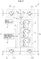
- Fig. 4 is a circuit diagram illustrating a first modification of the chopper circuit according to the first embodiment of the present disclosure.
- four semiconductor valve devices i.e., first switch units 11-1 and 11-2 and second switch units 12-1 and 12-2 are provided as a main power converter 10.
- Each of the first switch units 11-1 and 11-2 and the second switch units 12-1 and 12-2 is implemented as a semiconductor valve device capable of unidirectional current cutoff, and is formed by a semiconductor switching element which conducts electricity in one direction in the ON state, and a feedback diode connected in antiparallel with the semiconductor switching element.
- the first switch unit 11-1 is interposed between a first external connection terminal T 1 and a connection point P 1 .
- the first switch unit 11-2 is interposed between a ground terminal G 1 in a first external connection terminal and a connection point P 2 .
- the second switch unit 12-1 is interposed between the connection point P 1 and a second external connection terminal T 2 .
- the second switch unit 12-2 is interposed between the connection point P 2 and a ground terminal G 2 in a second external connection terminal.
- the second switch unit 12-1 is connected in series with the first switch unit 11-1 at the connection point P 1 to conduct electricity in the same direction as that in which the first switch unit 11-1 conducts electricity in the ON state.
- the second switch unit 12-2 is connected in series with the first switch unit 11-2 at the connection point P 2 to conduct electricity in the same direction as that in which the first switch unit 11-2 conducts electricity in the ON state.
- the first switch unit 11-2 and the second switch unit 12-2 are always set ON, and while one of the first switch unit 11-1 and the second switch unit 12-1 is controlled to be ON, the other switch unit is controlled to be OFF.
- the chopper circuit 1 illustrated in Fig. 4 is equivalent to the chopper circuit illustrated in Fig. 1 .
- the first switch unit 11-1 and the second switch unit 12-1 are always set ON, and while one of the first switch unit 11-2 and the second switch unit 12-2 is controlled to be ON, the other switch unit is controlled to be OFF.
- Fig. 5 is a circuit diagram illustrating a second modification of the chopper circuit according to the first embodiment of the present disclosure.
- four semiconductor valve devices i.e., first switch units 11-1 and 11-2 and second switch units 12-1 and 12-2 are provided as a main power converter 10.
- Each of the first switch units 11-1 and 11-2 and the second switch units 12-1 and 12-2 is implemented as a semiconductor valve device capable of unidirectional current cutoff, and is formed by a semiconductor switching element which conducts electricity in one direction in the ON state, and a feedback diode connected in antiparallel with the semiconductor switching element.
- the first switch units 11-1 and 11-2 are interposed between a first external connection terminal T 1 and a connection point P 1 .
- the first switch unit 11-1 is provided to conduct electricity in the direction opposite to that in which the first switch unit 11-2 conducts electricity in the ON state.
- the first switch units 11-1 and 11-2 may be interchanged with each other.
- the second switch units 12-1 and 12-2 are interposed between the connection point P 1 and a second external connection terminal T 2 .
- the second switch unit 12-1 is provided to conduct electricity in the direction opposite to that in which the second switch unit 12-2 conducts electricity in the ON state.
- the second switch units 12-1 and 12-2 may be interchanged with each other.
- the second switch unit 12-1 is provided to conduct electricity in the same direction as that in which the first switch unit 11-1 conducts electricity in the ON state.
- the second switch unit 12-2 is provided to conduct electricity in the same direction as that in which the first switch unit 11-2 conducts electricity in the ON state.
- the first switch unit 11-1 and the second switch unit 12-1 are always set ON, and while one of the first switch unit 11-2 and the second switch unit 12-2 is controlled to be ON, the other switch unit is controlled to be OFF.
- each of the first switch unit 11 and the second switch unit 12 as a semiconductor valve device capable of bidirectional current cutoff, in the chopper circuit 1 illustrated in Fig. 1 .
- a snubber circuit for suppressing overvoltages may be connected in parallel with the semiconductor valve device of each of the first switch unit 11 and the second switch unit 12 in the chopper circuit 1 illustrated in Fig. 1 , and the semiconductor valve device of each of the first switch units 11-1 and 11-2 and the second switch units 12-1 and 12-2 in the chopper circuits 1 illustrated in Figs. 4 and 5 .
- FIG. 6 illustrates graphs of ideal waveforms in respective portions of the chopper circuit according to the first embodiment of the present disclosure, and depicts in (A), the relationship between a triangular wave and a modulation wave used in a switch control unit; in (B), a voltage appearing across the two ends of a first switch unit; in (C), a voltage appearing across the two ends of a second switch unit; in (D), a voltage output from an auxiliary power converter; in (E), an inductor current; and in (F), currents flowing through the first switch unit and the second switch unit.
- a triangular wave v tri is indicated by a solid line
- a modulation wave d is indicated by an alternate long and short dashed line.
- a current i u1 flowing through the first switch unit is indicated by a solid line
- a current i u2 flowing through the second switch unit is indicated by a broken line.
- ON and OFF of the first switch unit 11 and the second switch unit 12 are determined by the switch control unit 16, based on the result of comparison between the modulation wave d and the triangular wave v tri that takes a minimum value of 0 and a maximum value of 1.
- the modulation wave d is determined by the relationship between the first DC voltage v dc1 and the second DC voltage v dc2 .
- the switch control unit 16 controls one of the first switch unit 11 and the second switch unit 12 to be ON and controls the other switch unit to be OFF. For example, when, as illustrated in Fig.
- the triangular wave v tri is smaller than the modulation wave d
- the switch control unit 16 controls the first switch unit 11 to be ON and controls the second switch unit 12 to be OFF.
- Fig. 6(C) the voltage appearing across the two ends of the first switch unit 11
- v S2u v dc1 - v dc2
- the triangular wave v tri is larger than the modulation wave d
- the switch control unit 16 controls the first switch unit 11 to be OFF and controls the second switch unit 12 to be ON.
- the semiconductor power converter control unit 15 controls the power conversion operation of the semiconductor power converter 13 (auxiliary power converter 19) so that an inductor current i u containing a DC component and an AC component having a predetermined period flows through the inductor 14.
- I dc for I dc > 0
- I ac for I ac > 0
- f SM be the carrier frequency of the triangular wave v tri
- the voltage v u output from the auxiliary power converter 19 contains a voltage term v fu which outputs v dc1 when the first switch unit 11 is ON and outputs v dc2 when the second switch unit 12 is ON, as presented in equation (2) as feedforward control ( Fig. 6(D) ).
- the voltage term v fu is higher than the remaining voltage terms contained in the voltage v u output from the auxiliary power converter 19, and the voltage v u output from the auxiliary power converter 19, therefore, can be regarded to be nearly equal to the voltage term v fu (v u ⁇ v fu ).
- the voltage term v fu equivalently contains a DC voltage and an AC voltage having the same frequency as the carrier frequency f SM .
- the auxiliary power converter 19 may be preferably controlled to adjust the power "v fu ⁇ i u " of the auxiliary power converter 19 to zero on average.
- the semiconductor power converter control unit 15 controls the power conversion operation of each semiconductor power converter 13 (auxiliary power converter 19) so that a current having the DC component I dc superimposed on the AC component I ac flows through the inductor 14 as the inductor current i u .
- the AC component contained in the inductor current i u is 180° out of phase with that when power flow is directed from the side of the first DC voltage v dc1 to that of the second DC voltage v dc2 .
- both the current i u1 flowing through the first switch unit 11 and the current i u2 flowing through the second switch unit 12 upon a change in voltage are zero. This means that the first switch unit 11 and the second switch unit 12 in an ideal state cause no switching losses.
- the phase ⁇ is determined by the first DC voltage v dc1 and the second DC voltage v dc2 , and is independent of the AC component I ac of the inductor current i u . This means that the phase ⁇ takes a value independent of the amount of power transmission.
- Equation (11) represents a quadratic equation for the phase ⁇ , and solving equation (11) for the phase ⁇ yields the following equation: [Math.
- ⁇ ⁇ 2 V dc 1 + V dc 2 V dc 1 ⁇ V dc 2 ⁇ 1 2 ⁇ 2 V dc 1 + V dc 2 V dc 1 ⁇ V dc 2 2 ⁇ 8
- the modulation wave d is determined based on equation (14), and the phase ⁇ is determined based on equation (13).
- the switch control unit 16 controls the first switch unit 11 to be ON and controls the second switch unit 12 to be OFF.
- the switch control unit 16 controls the first switch unit 11 to be OFF and controls the second switch unit 12 to be ON.
- the switch control unit 16 performs switching from ON to OFF and switching from OFF to ON for the first switch unit 11 and the second switch unit 12, at the phases ⁇ and ⁇ - ⁇ in which the current output from the semiconductor power converter 13 is controlled to be zero by the semiconductor power converter control unit 15.
- the above-mentioned method for determining the phase ⁇ assumes an ideal state in which each converter has zero loss. In the ideal state, when the phase of the current output from the semiconductor power converter 13 by the semiconductor power converter control unit 15 is ⁇ and ⁇ - ⁇ , this current output from the semiconductor power converter 13 is zero. In an actual chopper circuit 1, however, since each converter in the chopper circuit 1 has any loss, even when the phase of the current output from the semiconductor power converter 13 by the semiconductor power converter control unit 15 is ⁇ and ⁇ - ⁇ , this current output from the semiconductor power converter 13 is not zero, and a minute current flows.
- the switch control unit 16 performs switching from ON to OFF and switching from OFF to ON for the first switch unit 11 and the second switch unit 12, at the phases ⁇ and ⁇ - ⁇ in which the current output from the semiconductor power converter 13 is controlled to be equal to or lower than a predetermined value by the semiconductor power converter control unit 15.
- the predetermined value means herein a value sufficiently smaller than the rated current of the semiconductor power converter 13.
- the predetermined value is set to a value of, e.g., about 0% to 10% of the rated current of the semiconductor power converter 13, but it may be set to a value larger than 10% of the rated current of the semiconductor power converter 13, depending on the environment under which the chopper circuit 1 is applied.
- Fig. 7 is a circuit diagram illustrating a chopper circuit system formed by parallel-connected chopper circuits according to the first embodiment of the present disclosure.
- a chopper circuit system 1000 is formed by chopper circuits 1 connected in parallel with each other.
- the number of chopper circuits 1 is represented by the number of units M (where M is a natural number), and the respective chopper circuits 1 are represented as a first unit, a second unit, ..., an Mth unit.
- the auxiliary power converter 19 in each chopper circuit 1 is represented as an equivalent controlled voltage source v u .
- Each unit (chopper circuit 1) is connected in parallel with a common DC power supply v dc1 on the high-voltage side, and connected in parallel with a common DC power supply v dc2 on the low-voltage side.
- the triangular wave initial phase of the main power converter 10 in each unit is shifted by 180/M degrees for each unit.
- the phase of each inductor current i u is similarly shifted by 180/M degrees.
- the number of units M is other than three as well, a control system can be similarly formed, i.e., the following description is applicable.
- the first unit of the chopper circuit 1 will be referred to as a u-phase power converter hereinafter
- the second unit of the chopper circuit 1 will be referred to as a v-phase power converter hereinafter
- the third unit of the chopper circuit 1 will be referred to as a w-phase power converter hereinafter, for the sake of convenience.
- the u, v, and w phases of the chopper circuit system 1000 are different in meaning from the original u, v, and w phases of the three-phase power converter.
- the control system of the chopper circuit system 1000 is formed by an inductor current control system (power control system) and a DC capacitor voltage control system.
- the configuration of the inductor current control system (power control system) of the chopper circuit system 1000 will be described first.
- the inductor current control system of the chopper circuit system 1000 can employ a current control system based on coordinate transformation generally applied in a power conversion system. Let i u , i v , and i w be the inductor currents of the respective phases.
- the inductor currents i u , i v , and i w of the respective phases are formed by a positive-phase-sequence current and a negative-phase-sequence current which are 120° out of phase with each other, and an in-phase, zero-phase-sequence current.
- a d-axis current i d and a q-axis current i q can be calculated by applying d-q coordinate transformation to the inductor currents i u , i v , and i w of the respective phases.
- the calculation of the d-axis current i d and the q-axis current i q uses a reference sinusoidal wave having the same frequency f SM as that of the triangular wave v tri applied to the first switch unit 11 and the second switch unit 12 in the chopper circuit 1. More specifically, a sinusoidal current having a frequency of 50 [Hz] or 60 [Hz] is controlled in a general power conversion system, while a sinusoidal current having the carrier frequency f SM (e.g., on the order of several hundred hertz or more) is controlled in the chopper circuit system 1000.
- f SM carrier frequency
- the d-axis current i d represents a current component contributing to power transmission between the first DC voltage v dc1 and the second DC voltage v dc2
- the q-axis current i q represents a current component which does not contribute to power transmission between the first DC voltage v dc1 and the second DC voltage v dc2
- the d-axis current i d of the chopper circuit system 1000 corresponds to an active current in the general power conversion system
- the q-axis current i q of the chopper circuit system 1000 corresponds to a reactive current in the general power conversion system.
- Fig. 8 is a block diagram illustrating a positive-phase-sequence current control system in a chopper circuit system formed by three parallel-connected chopper circuits according to the first embodiment of the present disclosure.
- a command value i d * for the d-axis current i d contributing to power transmission between the first DC voltage v dc1 and the second DC voltage v dc2 is determined by a power flow command value p* issued from the side of the first DC voltage v dc1 to that of the second DC voltage v dc2 .
- the average power on the side of the first DC voltage v dc1 is given by the following equation: [Math.
- the auxiliary power converter 19 absorbs power from the side of the first DC voltage v dc1 when the first switch unit 11 is ON and the second switch unit 12 is OFF, and the auxiliary power converter 19 emits power to the side of the second DC voltage v dc2 when the first switch unit 11 is OFF and the second switch unit 12 is ON.
- the one-period average of the power flowing into and out of the auxiliary power converter 19 is zero.
- DC capacitor voltage control may be preferably applied to the capacitor in each semiconductor power converter 13 (chopper cell).
- the DC capacitor voltage control system of the chopper circuit system 1000 is formed by a DC voltage collective control system, an interphase balance control system, a zero-phase-sequence current control system, and an intercell balance control system.
- Fig. 9 is a block diagram illustrating a DC voltage collective control system within a DC capacitor voltage control system in the chopper circuit system formed by the three parallel-connected chopper circuits according to the first embodiment of the present disclosure.
- the DC voltage collective control system forms a feedback loop which allows an arithmetic mean v Cave of DC capacitor voltages used for all the semiconductor power converters 13 (chopper cells) in the chopper circuit system 1000 to follow a command value v C *. More specifically, this configuration is implemented by adjusting a DC component i 0dc contained in a zero-phase-sequence current i 0 .
- v Cave is given by the following equation: [Math.
- v Cave 1 3 v Cuave + v Cvave + v CWave
- Fig. 10 is a block diagram illustrating an interphase balance control system within the DC capacitor voltage control system in the chopper circuit system formed by the three parallel-connected chopper circuits according to the first embodiment of the present disclosure.
- the interphase balance control system is implemented using a carrier frequency component i 0ac contained in the zero-phase-sequence current i 0 . Referring to Fig.
- sincot represents a component in phase with the inductor current i u in the chopper circuit 1 of the first unit
- sin( ⁇ t - 2 ⁇ /3) represents a component in phase with the inductor current i v in the chopper circuit 1 of the second unit
- sin( ⁇ t - 4 ⁇ /3) represents a component in phase with the inductor current i w in the chopper circuit 1 of the third unit.
- a command value i 0ac * for the carrier frequency component i 0ac contained in the zero-phase-sequence current i 0 generates a component in phase with the inductor current i u in the chopper circuit 1 of the first unit, as is obvious from Fig. 10 .
- v Cave increases as the carrier frequency component i 0ac contained in the zero-phase-sequence current i 0 forms a positive active power with the AC component contained in the voltage term v fu in Fig. 6 .
- the remaining phases the chopper circuits 1 of the remaining units).
- Fig. 11 is a block diagram illustrating a zero-phase-sequence current control system within the DC capacitor voltage control system in the chopper circuit system formed by the three parallel-connected chopper circuits according to the first embodiment of the present disclosure.
- the zero-phase-sequence current control system forms a feedback loop which allows the zero-phase-sequence current i 0 to follow a command value "i 0dc * + i 0ac *," and generates a voltage command value v 0 * common to each phase (each unit).
- Fig. 12 is a block diagram illustrating an individual balance control system within the DC capacitor voltage control system in the chopper circuit system formed by the three parallel-connected chopper circuits according to the first embodiment of the present disclosure.
- the individual balance control system achieves a voltage balance by forming an active power between the inductor current and the voltage output from each semiconductor power converter 13 (chopper cell).
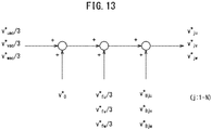
- Fig. 13 is a block diagram illustrating a voltage command value issued to each semiconductor power converter (chopper cell) in the chopper circuit system formed by the three parallel-connected chopper circuits according to the first embodiment of the present disclosure.
- v fu *, v fv *, and v fw * represent the voltage command values of a feedforward term, and v fu *, for example, is given by the following equation: [Math. 21]
- v fu ⁇ ⁇ v dc 1 First Switch Unit : ON
- Second Switch Unit OFF v dc 2 First Switch Unit : OFF
- Second Switch Unit ON
- Each of chopper cell voltage command values v ju *, v jv *, and v jw * (j: 1 - N) is normalized by the DC capacitor voltage and then compared with a triangular wave having a carrier frequency f SA and taking a maximum value of 1 and a minimum value of 0.
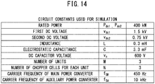
- Fig. 14 is a table illustrating circuit constants used for simulation of the chopper circuit system formed by the three parallel-connected chopper circuits according to the first embodiment of the present disclosure, in which the simulation used "PSCAD/EMTDC.”
- the number of units M of the chopper circuit system 1000 was three, and the number (the number of chopper cells) N of semiconductor power converters 13 provided in the chopper circuit 1 serving as each unit was set to three.
- the first DC voltage v dc1 was set to 1.5 [kV]
- the second DC voltage v dc2 was set to 0.75 [kV]
- the DC capacitor voltage V C of the capacitor in each semiconductor power converter 13 (chopper cell) was set to 0.6 [kV].
- the carrier frequency f SM of the main power converter 10 in each unit was set to 450 [Hz]
- This simulation aims to confirm the principle, and therefore assumes an ideal state. In other words, assuming an analog control system having zero control delay, ideal switches having zero dead time were used.
- Fig. 15 illustrates graphs of simulated waveforms when a power of 400 [kW] is transmitted from a first DC voltage side to a second DC voltage side in the chopper circuit system formed by the three parallel-connected chopper circuits according to the first embodiment of the present disclosure, and depicts in (A), inductor currents for respective units; in (B), voltages respectively appearing across the two ends of a first switch unit and the two ends of a second switch unit in a first unit; in (C), currents respectively flowing through the first switch unit and the second switch unit in the first unit; in (D), currents respectively flowing on the first DC voltage side and the second DC voltage side in the chopper circuit system; and in (E), DC capacitor voltages for capacitors in the semiconductor power converters (chopper cells).
- each of the DC capacitor voltages v C1u , v C1v , and v C1w of the capacitors in the semiconductor power converters 13 (chopper cells) illustrated in Fig. 15(E) contains DC and AC components, and the DC component of these components satisfactorily follows 600 [V] that is the command value.
- the AC component an AC component having a frequency of 450 [Hz] is present, but its magnitude is sufficiently lower than that of the DC component.
- Fig. 16 illustrates graphs of simulated waveforms when a power of 400 [kW] is transmitted from the second DC voltage side to the first DC voltage side in the chopper circuit system formed by the three parallel-connected chopper circuits according to the first embodiment of the present disclosure, and depicts in (A), inductor currents for the respective units; in (B), voltages respectively appearing across the two ends of the first switch unit and the two ends of the second switch unit in the first unit; in (C), currents respectively flowing through the first switch unit and the second switch unit in the first unit; in (D), currents respectively flowing on the first DC voltage side and the second DC voltage side in the chopper circuit system; and in (E), DC capacitor voltages for the capacitors in the semiconductor power converters (chopper cells).
- Fig. 16 illustrates a simulation result obtained when power is transmitted in the direction (from the second DC voltage side to the first DC voltage side) opposite to that in the above-mentioned simulation of Fig. 15 .
- Fig. 17 illustrates graphs of simulated waveforms when the direction to transmit a power of 400 [kW] is reversed between the first DC voltage side and the second DC voltage side at a time instant of 5 ms in the chopper circuit system formed by the three parallel-connected chopper circuits according to the first embodiment of the present disclosure, and depicts in (A), inductor currents for the respective units; in (B), voltages respectively appearing across the two ends of the first switch unit and the two ends of the second switch unit in the first unit; in (C), currents respectively flowing through the first switch unit and the second switch unit in the first unit; in (D), currents respectively flowing on the first DC voltage side and the second DC voltage side in the chopper circuit system; and in (E), DC capacitor voltages for the capacitors in the semiconductor power converters (chopper cells).
- the chopper circuit according to the first embodiment of the present disclosure has been described above.
- a chopper circuit according to a second embodiment of the present disclosure will be described subsequently.
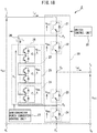
- Fig. 18 is a circuit diagram illustrating a chopper circuit according to a second embodiment of the present disclosure.
- a chopper circuit 2 bidirectionally converts a voltage between a first DC voltage v dc1 across a pair of first external connection terminals T 1 and G 1 and a second DC voltage v dc2 across a pair of second external connection terminals T 2 and G 2 .
- a DC power supply is connected to one of a set of the first external connection terminals T 1 and G 1 and a set of the second external connection terminals T 2 and G 2 , and a load or another DC power supply is connected to the other set of external connection terminals.
- the chopper circuit 2 When, for example, a DC power supply is connected to the first external connection terminals T 1 and G 1 , and a load is connected to the second external connection terminals T 2 and G 2 , the chopper circuit 2 operates as a step-down chopper.
- a voltage output from the DC power supply is used as the first DC voltage v dc1
- a voltage applied to the load is used as the second DC voltage v dc2 .
- the chopper circuit 2 When, as another example, a load is connected to the first external connection terminals T 1 and G 1 , and a DC power supply is connected to the second external connection terminals T 2 and G 2 , the chopper circuit 2 operates as a step-up chopper.
- a voltage applied to the load is used as the first DC voltage v dc1
- a voltage output from the DC power supply is used as the second DC voltage v dc2 .
- a DC power supply may be connected to the first external connection terminals T 1 and G 1 , and another DC power supply may be connected to the second external connection terminals T 2 and G 2 .
- the chopper circuit 2 includes a first switch unit 21, a second switch unit 22, a third switch unit 23, a fourth switch unit 24, a semiconductor power converter 25, and an inductor 26.
- the chopper circuit 2 further includes a semiconductor power converter control unit 27 and a switch control unit 28 as its control system.
- the first switch unit 21, the second switch unit 22, the third switch unit 23, and the fourth switch unit 24 are implemented as semiconductor valve devices capable of unidirectional current cutoff.
- Each of the first switch unit 21, the second switch unit 22, the third switch unit 23, and the fourth switch unit 24 is formed by a semiconductor switching element which conducts electricity in one direction in the ON state, and a feedback diode connected in antiparallel with the semiconductor switching element.
- Examples of the semiconductor switching element may include an IGBT, an SiC (Silicon Carbide)-MOSFET (Metal-Oxide-Semiconductor Field-Effect Transistor), a thyristor, a GTO (Gate Turn-OFF Thyristor), and a transistor, but the type of semiconductor switching element itself does not limit the present invention, and other types of semiconductor elements may also be used.
- a snubber circuit for suppressing overvoltages may be connected in parallel with the semiconductor valve device of each of the first switch unit 21, the second switch unit 22, the third switch unit 23, and the fourth switch unit 24.
- the first switch unit 21, the second switch unit 22, the third switch unit 23, and the fourth switch unit 24 are connected in series with each other to conduct electricity in the same direction in the ON state.
- the connection point between the first switch unit 21 and the second switch unit 22 is represented by P 3
- the connection point between the second switch unit 22 and the third switch unit 23 is represented by P 4
- the connection point between the third switch unit 23 and the fourth switch unit 24 is represented by P 5
- the connection point on the side of the fourth switch unit 24 opposite to that of the fourth switch unit 24 on which the third switch unit 23 is connected to the fourth switch unit 24 is represented by P 6 .
- a terminal on the side opposite to the connection point P 3 between the first switch unit 21 and the second switch unit 22 is used as a positive electrode terminal T 1 of the first external connection terminals.
- a terminal on the side opposite to the connection point P 5 between the third switch unit 23 and the fourth switch unit 24 is used as a ground terminal G 1 of the first external connection terminals.
- the positive electrode terminal T 1 and the ground terminal G 1 form a pair of first external connection terminals.
- a positive electrode terminal T 2 of the second external connection terminals is provided on wiring extending from the connection point P 4 between the second switch unit 22 and the third switch unit 23.
- a ground terminal G 2 of the second external connection terminals is provided on wiring extending from the connection point P 6 on the side of the fourth switch unit 24 opposite to that of the fourth switch unit 24 on which the third switch unit 23 is connected to the fourth switch unit 24.
- the positive electrode terminal T 2 and the ground terminal G 2 form a pair of second external connection terminals.
- the forward voltage (i.e., the potential difference between the positive electrode terminal T 1 of the first external connection terminals and the connection point P 3 ) of the first switch unit 21 is represented by v S1u .
- the forward voltage (i.e., the potential difference between the connection points P 3 and P 4 ) of the second switch unit 22 is represented by v S2u .
- the forward voltage (i.e., the potential difference between the connection points P 4 and P 5 ) of the third switch unit 23 is represented by v S3u .
- the forward voltage (i.e., the potential difference between the connection points P 5 and P 6 ) of the fourth switch unit 24 is represented by v S4u .
- the current flowing between the positive electrode terminal T 1 of the first external connection terminals and the connection point P 3 is represented by i u1
- the current flowing between the connection point P 4 and the positive electrode terminal T 2 of the second external connection terminals is represented by i u2 .
- a set of power converters formed by the first switch unit 21, the second switch unit 22, the third switch unit 23, and the fourth switch unit 24 will be referred to as a main power converter 20 hereinafter. While one of a set of the first switch unit 21 and the third switch unit 23 and a set of the second switch unit 22 and the fourth switch unit 24 is controlled to be ON, the other set of switch units is controlled to be OFF, as will be described later.
- the inductor 26 and a variable controlled voltage source which uses the semiconductor power converter 25 are provided on wiring connecting the connection point P 3 between the first switch unit 21 and the second switch unit 22 to the connection point P 5 between the third switch unit 23 and the fourth switch unit 24.
- the semiconductor power converter 25 is provided as one semiconductor power converter 25 alone or a plurality of semiconductor power converters 25 cascaded to each other, on the wiring connecting the connection point P 3 to the connection point P 5 .
- one or more semiconductor power converters 25 will be referred to as an auxiliary power converter 29 hereinafter.
- first DC side the side on which the inductor 26 (to be described later) is connected to it
- second DC side the side on which another semiconductor power converter 25 different from the semiconductor power converter 25 connected to the inductor 26 is connected to the latter semiconductor power converter 25
- first DC side the side on which another semiconductor power converter 25 different from the semiconductor power converter 25 connected to the inductor 26 is connected to the latter semiconductor power converter 25
- first DC side the side on which another semiconductor power converter 25 different from the semiconductor power converter 25 connected to the inductor 26 is connected to the latter semiconductor power converter 25
- second DC side the DC side opposite to the "first DC side”
- the semiconductor power converter 25 is implemented as a bidirectional chopper cell including a DC/DC converter 131 and a capacitor 132, as illustrated in Fig. 2 .
- the semiconductor power converter 25 is implemented as a chopper cell formed by two series-connected semiconductor switches and a DC capacitor connected in parallel with the two semiconductor switches, and having, as an output terminal, each terminal of one semiconductor switch of the two semiconductor switches.
- the DC/DC converter 131 and the capacitor 132 are the same as those described with reference to Fig. 2 .
- the DC/DC converter 131 is operated to initially charge the capacitor 132.
- the voltage of the DC capacitor of each semiconductor power converter 25 is defined as v Cju
- the voltage on the first DC side of the auxiliary power converter 29 is defined as v u .
- the inductor 26 and the auxiliary power converter 29 operate as a controlled current source by controlling an inductor current i u using the auxiliary power converter 29.
- an auxiliary power converter is implemented by cascading the semiconductor power converters 25 (chopper cells) to each other, but any arbitrary semiconductor power converter having the same functions can also be substituted for the auxiliary power converter.
- the inductor 26 is connected in series with the semiconductor power converter 25 on the wiring connecting the connection point P 3 between the first switch unit 21 and the second switch unit 22 to the connection point P 5 between the third switch unit 23 and the fourth switch unit 24.
- An inductor current flowing through the inductor 26 is defined as i u .
- the semiconductor power converter 25 and the inductor 26 are, therefore, provided on the same wiring branching from the connection point P 3 located on wiring connecting the first switch unit 21 to the second switch unit 22 in the main power converter 20.
- the inductor 26 is interposed between the connection point P 3 and the semiconductor power converter 25, and the second external connection terminals T 2 and G 2 are placed at the connection point P 6 (i.e., on the side of the set of the semiconductor power converters 25 opposite to that of the set of the semiconductor power converters 25 on which the inductor 26 is connected to the semiconductor power converter 25) on the side of the auxiliary power converter 29 opposite to that of the auxiliary power converter 29 on which the inductor 26 is connected to the auxiliary power converter 29, but the order of placement of the semiconductor power converter 25 and the inductor 26 can be freely designed, as illustrated in Fig. 3 , on the wiring provided with the semiconductor power converters 25 between the connection points P 3 and P 5 , as in the above-described first embodiment.
- the semiconductor power converter control unit 27 controls the power conversion operation of the semiconductor power converter 25 to output a current containing a DC component and an AC component having a predetermined period.
- the switch control unit 28 controls one of the set of the first switch unit 21 and the third switch unit 23 and the set of the second switch unit 22 and the fourth switch unit 24 to be ON and controls the other set of switch units to be OFF.
- the switch control unit 28 performs switching from ON to OFF and switching from OFF to ON for each of the set of the first switch unit 21 and the third switch unit 23 and the set of the second switch unit 22 and the fourth switch unit 24 when the value of the current output from the semiconductor power converter 25 is controlled to be equal to or smaller than a predetermined value by the semiconductor power converter control unit 27.
- the predetermined value means herein a value sufficiently smaller than the rated current of the semiconductor power converter 25.
- the predetermined value is set to a value of, e.g., about 0% to 10% of the rated current of the semiconductor power converter 25, but it may be set to a value larger than 10% of the rated current of the semiconductor power converter 25, depending on the environment under which the chopper circuit 2 is applied.
- the semiconductor power converter control unit 27 and the switch control unit 28 may be constructed in, e.g., software program form, or may be constructed as a combination of various electronic circuits and a software program. When, for example, these units are constructed in software program form, the function of each of the above-mentioned units can be implemented by causing an arithmetic processing unit to operate in accordance with the software program. Alternatively, the semiconductor power converter control unit 27 and the switch control unit 28 may be implemented as a semiconductor integrated circuit in which a software program for implementing the function of each of these units is written.
- the operation principle of the chopper circuit 2 according to the second embodiment of the present disclosure will be described subsequently.
- the operation principles of the semiconductor power converter control unit 27 and the switch control unit 28 are similar to those of the semiconductor power converter control unit 15 and the switch control unit 16 in the first embodiment.
- the chopper circuit 2 according to the second embodiment can bidirectionally convert a voltage between the first DC voltage v dc1 across the pair of first external connection terminals T 1 and G 1 and the second DC voltage v dc2 across the pair of second external connection terminals T 2 and G 2 .
- the chopper circuit 2 according to the second embodiment may preferably have a relationship "v dc1 > v dc2 " in which the first DC voltage v dc1 is higher than the second DC voltage v dc2 .
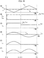
- Fig. 19 illustrates graphs of ideal waveforms in respective portions of the chopper circuit according to the second embodiment of the present disclosure, and depicts in (A), the relationship between a triangular wave and a modulation wave used in a switch control unit; in (B), voltages respectively appearing across the two ends of a first switch unit and the two ends of a second switch unit; in (C), a voltage output from an auxiliary power converter; in (D), an inductor current; in (E), a current flowing through the first switch unit; and in (F), a current flowing through the second switch unit.
- a triangular wave v tri is indicated by a solid line
- a modulation wave d is indicated by an alternate long and short dashed line.
- the operation of the chopper circuit 2 according to the second embodiment differs between the case where the second DC voltage v dc2 is lower than 1/2 of the first DC voltage v dc1 (v dc2 ⁇ 0.5v dc1 ) and the case where the second DC voltage v dc2 is higher than 1/2 of the first DC voltage v dc1 (v dc2 > 0.5v dc1 ), but the same operation principle is applicable to both cases.
- the case where the second DC voltage v dc2 is lower than 1/2 of the first DC voltage v dc1 (v dc2 ⁇ 0.5v dc1 ) will be described hereinafter.
- ON and OFF of the first switch unit 21 and the second switch unit 22 are determined by the switch control unit 28, based on the result of comparison between the modulation wave d and the triangular wave v tri that takes a minimum value of 0 and a maximum value of 1.
- the modulation wave d is determined by the relationship between the first DC voltage v dc1 and the second DC voltage v dc2 .
- the switch control unit 28 controls one of the set of the first switch unit 21 and the third switch unit 23 and the set of the second switch unit 22 and the fourth switch unit 24 to be ON and controls the other set of switch units to be OFF. For example, when, as illustrated in Fig.
- the triangular wave v tri is smaller than the modulation wave d
- the switch control unit 28 controls the set of the first switch unit 21 and the third switch unit 23 to be ON and controls the set of the second switch unit 22 and the fourth switch unit 24 to be OFF.
- Fig. 19(B) the voltage appearing across the two ends of the first switch unit 21
- v S2u v dc1 - v dc2
- the triangular wave v tri is larger than the modulation wave d
- the switch control unit 28 controls the set of the first switch unit 21 and the third switch unit 23 to be OFF and controls the set of the second switch unit 22 and the fourth switch unit 24 to be ON.
- the waveforms in the respective portions of the chopper circuit 2 according to the second embodiment are basically the same as those in the respective portions of the chopper circuit 1 according to the first embodiment, except for the current i u1 flowing between the positive electrode terminal T 1 of the first external connection terminals and the connection point P 3 , and the current i u2 flowing between the connection point P 4 and the positive electrode terminal T 2 of the second external connection terminals.
- the modulation wave d is determined based on equation (26), and the phase ⁇ is determined based on equation (25).
- the switch control unit 28 controls the set of the first switch unit 21 and the third switch unit 23 to be ON and controls the set of the second switch unit 22 and the fourth switch unit 24 to be OFF.
- the switch control unit 28 controls the set of the first switch unit 21 and the third switch unit 23 to be OFF and controls the set of the second switch unit 22 and the fourth switch unit 24 to be ON.
- the switch control unit 28 performs switching from ON to OFF and switching from OFF to ON for each of the set of the first switch unit 21 and the third switch unit 23 and the set of the second switch unit 22 and the fourth switch unit 24, at the phases ⁇ and ⁇ - ⁇ in which the current output from the semiconductor power converter 25 is controlled to be zero by the semiconductor power converter control unit 27.
- the above-mentioned method for determining the phase ⁇ assumes an ideal state in which each converter has zero loss. In the ideal state, when the phase of the current output from the semiconductor power converter 25 by the semiconductor power converter control unit 27 is ⁇ and ⁇ - ⁇ , this current output from the semiconductor power converter 25 is zero. In an actual chopper circuit 2, however, since each converter in the chopper circuit 2 has any loss, even when the phase of the current output from the semiconductor power converter 25 by the semiconductor power converter control unit 27 is ⁇ and ⁇ - ⁇ , this current output from the semiconductor power converter 25 is not zero, and a minute current flows.
- the switch control unit 28 performs switching from ON to OFF and switching from OFF to ON for each of the set of the first switch unit 21 and the third switch unit 23 and the set of the second switch unit 22 and the fourth switch unit 24, at the phases ⁇ and ⁇ - ⁇ in which the current output from the semiconductor power converter 25 is controlled to be equal to or lower than a predetermined value by the semiconductor power converter control unit 27.
- the predetermined value means herein a value sufficiently smaller than the rated current of the semiconductor power converter 25.
- the predetermined value is set to a value of, e.g., about 0% to 10% of the rated current of the semiconductor power converter 25, but it may be set to a value larger than 10% of the rated current of the semiconductor power converter 25, depending on the environment under which the chopper circuit 2 is applied.
- Fig. 20 is a circuit diagram illustrating a chopper circuit system formed by parallel-connected chopper circuits according to the second embodiment or a third embodiment of the present disclosure.
- the chopper circuit system 1000 is formed by chopper circuits 2 connected in parallel with each other.
- the number of chopper circuits 2 is represented by the number of units M (where M is a natural number), and the respective chopper circuits 2 are represented as a first unit, a second unit, ..., an Mth unit.
- Each unit (chopper circuit 2) is connected in parallel with a common DC power supply v dc1 on the high-voltage side, and connected in parallel with a common DC power supply v dc2 on the low-voltage side.
- the triangular wave initial phase of the main power converter 20 in each unit is shifted by 180/M degrees for each unit.
- the phase of each inductor current i u is similarly shifted by 180/M degrees.
- Fig. 21 is a table illustrating circuit constants used for simulation of a chopper circuit system formed by three parallel-connected chopper circuits according to the second embodiment of the present disclosure, in which the simulation used "PSCAD/EMTDC.”
- the number of units M of the chopper circuit system 1000 was three, and the number (the number of chopper cells) N of semiconductor power converters 25 provided in the chopper circuit 2 serving as each unit was set to three.
- the first DC voltage v dc1 was set to 1.5 [kV]
- the second DC voltage v dc2 was set to 0.6 [kV]
- the DC capacitor voltage V C of the capacitor in each semiconductor power converter 25 (chopper cell) was set to 0.45 [kV].
- the carrier frequency f SM of the main power converter 20 in each unit was set to 450 [Hz]
- This simulation aims to confirm the principle, and therefore assumes an ideal state. In other words, assuming an analog control system having zero control delay, ideal switches having zero dead time were used.
- Fig. 22 illustrates graphs of simulated waveforms when a power of 400 [kW] is transmitted from a first DC voltage side to a second DC voltage side in the chopper circuit system formed by the three parallel-connected chopper circuits according to the second embodiment of the present disclosure, and depicts in (A), inductor currents for respective units; in (B), voltages respectively appearing across the two ends of a first switch unit and the two ends of a second switch unit in a first unit; in (C), currents respectively flowing through the first switch unit and the second switch unit in the first unit; in (D), currents respectively flowing on the first DC voltage side and the second DC voltage side in the chopper circuit system; and in (E), DC capacitor voltages for capacitors in semiconductor power converters (chopper cells).
- A inductor currents for respective units
- B voltages respectively appearing across the two ends of a first switch unit and the two ends of a second switch unit in a first unit
- in (C) currents respectively flowing through the first switch unit and the second switch unit
- each of the DC capacitor voltages v C1u , v C1v , and v C1w of the capacitors in the semiconductor power converters 25 (chopper cells) illustrated in Fig. 22(E) contains DC and AC components, and the DC component of these components satisfactorily follows 450 [V] that is the command value.
- the AC component an AC component having a frequency of 450 [Hz] is present, but its magnitude is sufficiently lower than that of the DC component.
- Fig. 23 illustrates graphs of simulated waveforms when a power of 400 [kW] is transmitted from the second DC voltage side to the first DC voltage side in the chopper circuit system formed by the three parallel-connected chopper circuits according to the second embodiment of the present disclosure, and depicts in (A), inductor currents for the respective units; in (B), voltages respectively appearing across the two ends of the first switch unit and the two ends of the second switch unit in the first unit; in (C), currents respectively flowing through the first switch unit and the second switch unit in the first unit; in (D), currents respectively flowing on the first DC voltage side and the second DC voltage side in the chopper circuit system; and in (E), DC capacitor voltages for the capacitors in the semiconductor power converters (chopper cells).
- Fig. 23 illustrates a simulation result obtained when power is transmitted in the direction (from the second DC voltage side to the first DC voltage side) opposite to that in the above-mentioned simulation of Fig. 22 .
- Fig. 24 illustrates graphs of simulated waveforms when the direction to transmit a power of 400 [kW] is reversed between the first DC voltage side and the second DC voltage side at a time instant of 5 ms in the chopper circuit system formed by the three parallel-connected chopper circuits according to the second embodiment of the present disclosure, and depicts in (A), inductor currents for the respective units; in (B), voltages respectively appearing across the two ends of the first switch unit and the two ends of the second switch unit in the first unit; in (C), currents respectively flowing through the first switch unit and the second switch unit in the first unit; in (D), currents respectively flowing on the first DC voltage side and the second DC voltage side in the chopper circuit system; and in (E), DC capacitor voltages for the capacitors in the semiconductor power converters (chopper cells).
- the chopper circuit according to the second embodiment of the present disclosure has been described above.
- a chopper circuit according to a third embodiment of the present disclosure will be described subsequently.
- Fig. 25 is a circuit diagram illustrating a chopper circuit according to a third embodiment of the present disclosure.
- a chopper circuit 3 bidirectionally converts a voltage between a first DC voltage v dc1 across a pair of first external connection terminals T 1 and G 1 and a second DC voltage v dc2 across a pair of second external connection terminals T 2 and G 2 .
- a DC power supply is connected to one of a set of the first external connection terminals T 1 and G 1 and a set of the second external connection terminals T 2 and G 2 , and a load or another DC power supply is connected to the other set of external connection terminals.
- the chopper circuit 3 When, for example, a DC power supply is connected to the first external connection terminals T 1 and G 1 , and a load is connected to the second external connection terminals T 2 and G 2 , the chopper circuit 3 operates as a step-down chopper or a step-up chopper. In this case, a voltage output from the DC power supply is used as the first DC voltage v dc1 , and a voltage applied to the load is used as the second DC voltage v dc2 .
- the chopper circuit 3 When, as another example, a load is connected to the first external connection terminals T 1 and G 1 , and a DC power supply is connected to the second external connection terminals T 2 and G 2 , the chopper circuit 3 operates as a step-down chopper or a step-up chopper. In this case, a voltage applied to the load is used as the first DC voltage v dc1 , and a voltage output from the DC power supply is used as the second DC voltage v dc2 .
- a DC power supply may be connected to the first external connection terminals T 1 and G 1 , and another DC power supply may be connected to the second external connection terminals T 2 and G 2 .
- the chopper circuit 3 includes a first main power converter 30 including a first switch unit 31 and a second switch unit 32, a semiconductor power converter 33, an inductor 34, and a second main power converter 35 including a third switch unit 36 and a fourth switch unit 37.
- the chopper circuit 3 further includes a semiconductor power converter control unit 38 and a switch control unit 39 as its control system.
- the first switch unit 31, the second switch unit 32, the third switch unit 36, and the fourth switch unit 37 are implemented as semiconductor valve devices capable of unidirectional current cutoff.
- Each of the first switch unit 31, the second switch unit 32, the third switch unit 36, and the fourth switch unit 37 is formed by a semiconductor switching element which conducts electricity in one direction in the ON state, and a feedback diode connected in antiparallel with the semiconductor switching element.
- Examples of the semiconductor switching element may include an IGBT, an SiC (Silicon Carbide)-MOSFET (Metal-Oxide-Semiconductor Field-Effect Transistor), a thyristor, a GTO (Gate Turn-OFF Thyristor), and a transistor, but the type of semiconductor switching element itself does not limit the present invention, and other types of semiconductor elements may also be used.
- a snubber circuit for suppressing overvoltages may be connected in parallel with the semiconductor valve device of each of the first switch unit 31, the second switch unit 32, the third switch unit 36, and the fourth switch unit 37.
- the first switch unit 31 and the second switch unit 32 constituting the first main power converter 30 are connected in series with each other to conduct electricity in the same direction in the ON state.
- the connection point between the first switch unit 31 and the second switch unit 32 is represented by P 7 .
- the connection point on the side of the second switch unit 32 opposite to that of the second switch unit 32 on which the first switch unit 31 is connected to the second switch unit 32 is represented by P 8 .
- the third switch unit 36 and the fourth switch unit 37 constituting the second main power converter 35 are connected in series with each other to conduct electricity in the same direction in the ON state.
- the connection point between the third switch unit 36 and the fourth switch unit 37 is represented by P 9 .
- the connection point on the side of the third switch unit 36 opposite to that of the third switch unit 36 on which the fourth switch unit 37 is connected to the third switch unit 36 is represented by P 10 .
- a terminal on the opposite side of the first switch unit 31 with respect to the connection point P 7 between the first switch unit 31 and the second switch unit 32 is used as a positive electrode terminal T 1 of the first external connection terminals.
- a terminal on the opposite side of the second switch unit 32 with respect to the connection point P 7 between the first switch unit 31 and the second switch unit 32 is used as a ground terminal G 1 of the first external connection terminals.
- the positive electrode terminal T 1 and the ground terminal G 1 form a pair of first external connection terminals.
- the two electrode terminals on the side opposite to the connection point P 7 between the first switch unit 31 and the second switch unit 32 are used as a pair of first external connection terminals.
- a terminal on the opposite side of the fourth switch unit 37 with respect to the connection point P 9 between the third switch unit 36 and the fourth switch unit 37 is used as a negative electrode terminal T 2 of the second external connection terminals.
- a terminal on the opposite side of the third switch unit 36 with respect to the connection point P 9 between the third switch unit 36 and the fourth switch unit 37 is used as a ground terminal G 2 of the second external connection terminals.
- the negative electrode terminal T 2 and the ground terminal G 2 form a pair of second external connection terminals.
- the two electrode terminals on the side opposite to the connection point P 9 between the third switch unit 36 and the fourth switch unit 37 are used as a pair of second external connection terminals.
- the ground terminal G 1 of the first external connection terminals, the connection points P 8 and P 10 , and the ground terminal G 2 of the second external connection terminals are provided on the same wiring.
- the forward voltage (i.e., the potential difference between the positive electrode terminal T 1 of the first external connection terminals and the connection point P 7 ) of the first switch unit 31 is represented by v S1u .
- the forward voltage (i.e., the potential difference between the connection points P 7 and P 8 ) of the second switch unit 32 is represented by v S2u .
- the forward voltage (i.e., the potential difference between the connection points P 9 and P 10 ) of the third switch unit 36 is represented by v S3u .
- the forward voltage (i.e., the potential difference between the negative electrode terminal T 2 of the second external connection terminals and the connection point P 9 ) of the fourth switch unit 37 is represented by v S4u .
- the current flowing through the first switch unit 31 is represented by i u1
- the current flowing through the second switch unit 32 is represented by i u2
- the current flowing through the third switch unit 36 is represented by i u3
- the current flowing through the fourth switch unit 37 is represented by i u4 .
- the inductor 34 and a variable controlled voltage source which uses the semiconductor power converter 33 are provided on wiring connecting the connection point P 7 between the first switch unit 31 and the second switch unit 32 to the connection point P 9 between the third switch unit 36 and the fourth switch unit 37.
- the semiconductor power converter 33 is provided as one semiconductor power converter 33 alone or a plurality of semiconductor power converters 33 cascaded to each other, on the wiring connecting the connection point P 7 to the connection point P 9 .
- one or more semiconductor power converters 33 will be referred to as an auxiliary power converter 40 hereinafter.
- first DC side the side on which the inductor 34 (to be described later) is connected to it
- second DC side the side on which another semiconductor power converter 33 different from the semiconductor power converter 33 connected to the inductor 34 is connected to the latter semiconductor power converter 33
- first DC side the side on which another semiconductor power converter 33 different from the semiconductor power converter 33 connected to the inductor 34 is connected to the latter semiconductor power converter 33
- first DC side the side on which another semiconductor power converter 33 different from the semiconductor power converter 33 connected to the inductor 34 is connected to the latter semiconductor power converter 33
- second DC side the DC side opposite to the "first DC side”
- the number of cascades of the semiconductor power converters 33 is represented by j (where j is a natural number of 1 to N) hereinafter.
- High voltage resistance design of the chopper circuit 3 can easily be achieved simply by adjusting, as appropriate, the number of semiconductor power converters 33 to be cascaded to each other.
- the semiconductor power converter 33 is implemented as a bidirectional chopper cell including a DC/DC converter 131 and a capacitor 132, as illustrated in Fig. 2 .
- the semiconductor power converter 33 is implemented as a chopper cell formed by two series-connected semiconductor switches and a DC capacitor connected in parallel with the two semiconductor switches, and having, as an output terminal, each terminal of one semiconductor switch of the two semiconductor switches.
- the DC/DC converter 131 and the capacitor 132 are the same as those described with reference to Fig. 2 .
- the DC/DC converter 131 is operated to initially charge the capacitor 132.
- the voltage of the DC capacitor of each semiconductor power converter 33 is defined as v Cju
- the voltage on the first DC side of the auxiliary power converter 40 is defined as v u .
- the inductor 34 and the auxiliary power converter 40 operate as a controlled current source by controlling an inductor current i u using the auxiliary power converter 40.
- an auxiliary power converter is implemented by cascading the semiconductor power converters 33 (chopper cells) to each other, but any arbitrary semiconductor power converter having the same functions can also be substituted for the auxiliary power converter.
- the inductor 34 is connected in series with the semiconductor power converter 33 on the wiring connecting the connection point P 7 between the first switch unit 31 and the second switch unit 32 to the connection point P 9 between the third switch unit 36 and the fourth switch unit 37.
- a voltage applied to the two ends of the inductor 34 is defined as v u .
- An inductor current flowing through the inductor 34 is defined as i u .
- the semiconductor power converter 33 and the inductor 34 are, therefore, provided on wiring branching from wiring connecting the first switch unit 31 to the second switch unit 32.
- the inductor 34 is interposed between the connection point P 7 and the semiconductor power converter 33, but the order of placement of the semiconductor power converter 33 and the inductor 34 can be freely designed, as illustrated in Fig. 3 , on the wiring provided with the semiconductor power converters 33 between the connection points P 7 and P 9 , as in the above-described first and second embodiments.
- the semiconductor power converter control unit 38 controls the power conversion operation of the semiconductor power converter 33 to output a current containing a DC component and an AC component having a predetermined period.
- the switch control unit 39 controls one of the set of the first switch unit 31 and the third switch unit 36 and the set of the second switch unit 32 and the fourth switch unit 37 to be ON and controls the other set of switch units to be OFF.
- the switch control unit 39 performs switching from ON to OFF and switching from OFF to ON for each of the set of the first switch unit 31 and the third switch unit 36 and the set of the second switch unit 32 and the fourth switch unit 37 when the value of the current output from the semiconductor power converter 33 is controlled to be equal to or smaller than a predetermined value by the semiconductor power converter control unit 38.
- the predetermined value means herein a value sufficiently smaller than the rated current of the semiconductor power converter 33.
- the predetermined value is set to a value of, e.g., about 0% to 10% of the rated current of the semiconductor power converter 33, but it may be set to a value larger than 10% of the rated current of the semiconductor power converter 33, depending on the environment under which the chopper circuit 3 is applied.
- the semiconductor power converter control unit 38 and the switch control unit 39 may be constructed in, e.g., software program form, or may be constructed as a combination of various electronic circuits and a software program. When, for example, these units are constructed in software program form, the function of each of the above-mentioned units can be implemented by causing an arithmetic processing unit to operate in accordance with the software program.
- the semiconductor power converter control unit 38 and the switch control unit 39 may be implemented as a semiconductor integrated circuit in which a software program for implementing the function of each of these units is written.
- the operation principles of the semiconductor power converter control unit 38 and the switch control unit 39 are similar to those of the semiconductor power converter control unit 15 and the switch control unit 16 in the first embodiment.
- the modulation wave d is determined based on equation (14)
- the phase ⁇ is determined based on equation (13).
- the switch control unit 39 controls the set of the first switch unit 31 and the third switch unit 36 to be ON and controls the set of the second switch unit 32 and the fourth switch unit 37 to be OFF.
- the switch control unit 39 controls the set of the first switch unit 31 and the third switch unit 36 to be OFF and controls the set of the second switch unit 32 and the fourth switch unit 37 to be ON.
- the switch control unit 39 performs switching from ON to OFF and switching from OFF to ON for each of the set of the first switch unit 31 and the third switch unit 36 and the set of the second switch unit 32 and the fourth switch unit 37, at the phases ⁇ and ⁇ - ⁇ in which the current output from the semiconductor power converter 33 is controlled to be zero by the semiconductor power converter control unit 38.
- the above-mentioned method for determining the phase ⁇ assumes an ideal state in which each converter has zero loss. In the ideal state, when the phase of the current output from the semiconductor power converter 33 by the semiconductor power converter control unit 38 is ⁇ and ⁇ - ⁇ , this current output from the semiconductor power converter 33 is zero. In an actual chopper circuit 3, however, since each converter in the chopper circuit 3 has any loss, even when the phase of the current output from the semiconductor power converter 33 by the semiconductor power converter control unit 38 is ⁇ and ⁇ - ⁇ , this current output from the semiconductor power converter 33 is not zero, and a minute current flows.
- the switch control unit 39 performs switching from ON to OFF and switching from OFF to ON for each of the set of the first switch unit 31 and the third switch unit 36 and the set of the second switch unit 32 and the fourth switch unit 37, at the phases ⁇ and ⁇ - ⁇ in which the current output from the semiconductor power converter 33 is controlled to be equal to or lower than a predetermined value by the semiconductor power converter control unit 38.
- the predetermined value means herein a value sufficiently smaller than the rated current of the semiconductor power converter 33.
- the predetermined value is set to a value of, e.g., about 0% to 10% of the rated current of the semiconductor power converter 33, but it may be set to a value larger than 10% of the rated current of the semiconductor power converter 33, depending on the environment under which the chopper circuit 3 is applied.
- the chopper circuit 3 according to the third embodiment can bidirectionally convert a voltage between the first DC voltage v dc1 across the pair of first external connection terminals T 1 and G 1 and the second DC voltage v dc2 across the pair of second external connection terminals T 2 and G 2 .
- a voltage can be bidirectionally converted between the first DC voltage v dc1 and the second DC voltage v dc2 regardless of the relationship in value between the first DC voltage v dc1 and the second DC voltage v dc2 .
- the chopper circuit system 1000 is formed by chopper circuits 3 connected in parallel with each other.
- the number of chopper circuits 3 is represented by the number of units M (where M is a natural number), and the respective chopper circuits 3 are represented as a first unit, a second unit, ..., an Mth unit.
- Each unit (chopper circuit 3) is connected in parallel with a common DC power supply v dc1 on the first DC voltage side, and connected in parallel with a common DC power supply v dc2 on the second DC voltage side.
- the triangular wave initial phases of the first main power converter 30 and the second main power converter 35 in each unit are shifted by 180/M degrees for each unit.
- the phase of each inductor current i u is similarly shifted by 180/M degrees.
- Fig. 26 is a table illustrating circuit constants used for simulation of a chopper circuit system formed by three parallel-connected chopper circuits according to the third embodiment of the present disclosure, in which the simulation used "PSCAD/EMTDC.”
- the number of units M of the chopper circuit system 1000 was three, and the number (the number of chopper cells) N of semiconductor power converters 33 provided in the chopper circuit 3 serving as each unit was set to three.
- the first DC voltage v dc1 was set to 1.5 [kV]
- the second DC voltage v dc2 was set to 0.75 [kV]
- the DC capacitor voltage V C of the capacitor in each semiconductor power converter 33 (chopper cell) was set to 0.6 [kV].
- the carrier frequency f SM of the main power converter 10 in each unit was set to 450 [Hz]
- This simulation aims to confirm the principle, and therefore assumes an ideal state. In other words, assuming an analog control system having zero control delay, ideal switches having zero dead time were used.
- Fig. 27 illustrates graphs of simulated waveforms when a power of 400 [kW] is transmitted from a first DC voltage side to a second DC voltage side in the chopper circuit system formed by the three parallel-connected chopper circuits according to the third embodiment of the present disclosure, and depicts in (A), inductor currents for respective units; in (B), voltages respectively appearing across the two ends of a first switch unit and the two ends of a second switch unit in a first unit; in (C), voltages respectively appearing across the two ends of a third switch unit and the two ends of a fourth switch unit in the first unit; in (D), currents respectively flowing through the first switch unit and the second switch unit in the first unit; in (E), currents respectively flowing through the third switch unit and the fourth switch unit in the first unit; in (F), currents respectively flowing on the first DC voltage side and the second DC voltage side in the chopper circuit system; and in (G), DC capacitor voltages for capacitors in semiconductor power converters (chopper cells).
- A inductor current
- inductor currents i u , i v , and i w illustrated in Fig. 27(A) a negative DC current is obviously superimposed on an AC component having a frequency of 450 [Hz].
- the AC component having a frequency of 450 [Hz] has a sinusoidal waveform, and contains little harmonic current.
- voltages semiconductor valve device forward voltages
- v S1u , v S2u , v S3u , and v S4u respectively appearing across the two ends of the first switch unit 31, the two ends of the second switch unit 32, the two ends of the third switch unit 36, and the two ends of the fourth switch unit 37 in the first unit illustrated in Figs.
- each of the DC capacitor voltages v C1u , v C1v , and v C1w of the capacitors in the semiconductor power converters 33 (chopper cells) illustrated in Fig. 27(G) contains DC and AC components, and the DC component of these components satisfactorily follows 600 [V] that is the command value.
- the AC component an AC component having a frequency of 450 [Hz] is present, but its magnitude is sufficiently lower than that of the DC component.
Landscapes
- Engineering & Computer Science (AREA)
- Power Engineering (AREA)
- Dc-Dc Converters (AREA)
Abstract
Description
- The present disclosure relates to a chopper circuit which converts a voltage between a first DC voltage across first external connection terminals and a second DC voltage across second external connection terminals.
- In recent years, the application of a battery power storage system to a DC electric railway is in progress. For example, the use of a high-capacity lithium-ion battery mounted on a railway vehicle achieves a travel distance of 25 [km] or more on a single charge even when zero power is supplied from an overhead line.
- Since the overhead line voltage of a DC electric railway is generally different from the operating voltage of an energy storage element, voltage conversion (power conversion) may be preferably performed using a bidirectional chopper circuit.
Fig. 28 is a circuit diagram illustrating a general bidirectional chopper circuit. Abidirectional chopper circuit 101 includes a first switch unit (positive valve device) 121-1 and a second switch unit (negative valve device) 121-2 which are connected in series with each other to conduct electricity in the same direction in the ON state, and one of which is turned on when the other switch unit is turned off, and aninductor 113 connected to the connection point between the first switch unit 121-1 and the second switch unit 121-2. Each of the first switch unit 121-1 and the second switch unit 121-2 is formed by a semiconductor switching element which conducts electricity in one direction in the ON state, and a feedback diode connected in antiparallel with the semiconductor switching element. In a DC electric railway including a battery power storage system, a high-voltage side DC voltage Vdc1 corresponds to the overhead line voltage, and a low-voltage side DC voltage Vdc2 corresponds to the operating voltage of an energy storage element. When, for example, the standard voltage of the overhead line is Vdc1 = 1,500 [V], Vdc2 is set to about 600 [V] to 700 [V]. In recent years, a high-capacity bidirectional chopper having a converter capacity of 500 [kW] when used alone has been developed. In this case, a DC component of an inductor current iL has a current of 500 [A] or more. - In recent years, furthermore, a bidirectional chopper circuit using an auxiliary converter has been proposed.
- For example, a bidirectional chopper circuit which bidirectionally converts a voltage between a first DC voltage across a pair of first external connection terminals and a second DC voltage across a pair of second external connection terminals is known to include a main power converter including first and second switch units which are connected in series with each other to conduct electricity in the same direction in an ON state, and one of which is turned on when the other switch unit is turned off, the main power converter having, as the pair of first external connection terminals, two side terminals on a side opposite to a side on which the first switch unit is connected to the second switch unit, one single-phase full-bridge power converter or a plurality of single-phase full-bridge power converters cascaded to each other, provided on wiring branching from wiring connecting the first switch unit to the second switch unit, and an inductor connected in series with the single-phase full-bridge power converter on the wiring branching from the wiring connecting the first switch unit to the second switch unit, wherein the pair of second external connection terminals are provided at any position on the wiring that branches from the wiring connecting the first switch unit to the second switch unit, and is provided with the inductor and the single-phase full-bridge power converter (see, e.g., PTL 1).
- [PATENT LITERATURE 1]
International Publication No. WO 2017/038122 - In the chopper circuit, miniaturization and lightweight design of the inductor are posed as significant challenges, and are especially important when the inductor is mounted on a movable body such as a DC electric railway. Since the weight and the volume of the inductor are proportional to the stored energy of the inductor, the miniaturization and lightweight design of the inductor can be achieved by reducing the inductance of the inductor. The reduction in inductance, however, increases ripple currents contained in a current flowing through the inductor, and may therefore result in degradation in power quality or an unstable operation of the converter.
- In, e.g., the bidirectional chopper circuit illustrated in
Fig. 28 , theinductor 113 acts as a main factor making the system heavier in weight and larger in volume.DC circuit breakers - It is, therefore, desired to achieve a compact, lightweight, highly reliable, low-loss chopper circuit which causes no overvoltages.
- According to a first aspect of the present disclosure, a chopper circuit which converts a voltage between a first direct-current voltage on a first external connection terminal and a second direct-current voltage on a second external connection terminal includes a first switch unit including a first external connection terminal, a second switch unit connected in series with the first switch unit to conduct electricity in a direction identical to a direction in which the first switch unit conducts electricity in an ON state, and including a second external connection terminal on a side opposite to a side on which the first switch unit is connected to the second switch unit, at least one semiconductor power converter including one of a single semiconductor power converter and a plurality of semiconductor power converters cascaded to each other, provided on wiring branching from wiring connecting the first switch unit to the second switch unit, an inductor connected in series with the at least one semiconductor power converter, on wiring branching from wiring connecting the first switch unit to the second switch unit, a semiconductor power converter control unit configured to control a power conversion operation of the at least one semiconductor power converter to output a current containing a direct-current component and an alternating-current component having a predetermined period, and a switch control unit configured to control one of the first switch unit and the second switch unit to be ON and control the other switch unit to be OFF, the switch control unit being configured to perform switching from ON to OFF and switching from OFF to ON for the first switch unit and the second switch unit when a value of a current output from the at least one semiconductor power converter is controlled to be not more than a predetermined value by the semiconductor power converter control unit.
- As a chopper circuit according to a modification to the first aspect, a chopper circuit which converts a voltage between a first direct-current voltage on a first external connection terminal and a second direct-current voltage on a second external connection terminal may include a first switch unit including a first external connection terminal, a second switch unit connected in series with the first switch unit to conduct electricity in a direction identical to a direction in which the first switch unit conducts electricity in an ON state, and including a second external connection terminal on a side opposite to a side on which the first switch unit is connected to the second switch unit, at least one semiconductor power converter including one of a single semiconductor power converter and a plurality of semiconductor power converters cascaded to each other, provided on wiring branching from wiring connecting the first switch unit to the second switch unit, and an inductor connected in series with the at least one semiconductor power converter, on wiring branching from wiring connecting the first switch unit to the second switch unit, wherein the first switch unit may include two first switch units, and the second switch unit may include two second switch units.
- The chopper circuit according to the modification to the first aspect may further include a semiconductor power converter control unit configured to control a power conversion operation of the at least one semiconductor power converter to output a current containing a direct-current component and an alternating-current component having a predetermined period, and a switch control unit configured to control one of the first switch unit and the second switch unit to be ON and control the other switch unit to be OFF, the switch control unit being configured to perform switching from ON to OFF and switching from OFF to ON for the first switch unit and the second switch unit when a value of a current output from the at least one semiconductor power converter is controlled to be not more than a predetermined value by the semiconductor power converter control unit.
- According to a second aspect of the present disclosure, a chopper circuit which converts a voltage between a first direct-current voltage across a pair of first external connection terminals and a second direct-current voltage across a pair of second external connection terminals includes a first switch unit, a second switch unit, a third switch unit, and a fourth switch unit connected in series with each other to conduct electricity in an identical direction in an ON state, at least one semiconductor power converter including one of a single semiconductor power converter and a plurality of semiconductor power converters cascaded to each other, provided on wiring connecting a connection point between the first switch unit and the second switch unit to a connection point between the third switch unit and the fourth switch unit, an inductor connected in series with the at least one semiconductor power converter, on wiring connecting a connection point between the first switch unit and the second switch unit to a connection point between the third switch unit and the fourth switch unit, a semiconductor power converter control unit configured to control a power conversion operation of the at least one semiconductor power converter to output a current containing a direct-current component and an alternating-current component having a predetermined period, and a switch control unit configured to control one of a set of the first switch unit and the third switch unit and a set of the second switch unit and the fourth switch unit to be ON and control the other set of switch units to be OFF, the switch control unit being configured to perform switching from ON to OFF and switching from OFF to ON for each of a set of the first switch unit and the third switch unit and a set of the second switch unit and the fourth switch unit when a value of a current output from the at least one semiconductor power converter is controlled to be not more than a predetermined value by the semiconductor power converter control unit, wherein a terminal on a side opposite to a side on which the first switch unit is connected to the second switch unit, and a terminal on a side opposite to a side on which the third switch unit is connected to the fourth switch unit are provided as the pair of first external connection terminals, and a terminal on a side on which the second switch unit is connected to the third switch unit, and a terminal on a side of the fourth switch unit opposite to a side of the fourth switch unit on which the third switch unit is connected to the fourth switch unit are provided as the pair of second external connection terminals.
- According to a third aspect of the present disclosure, a chopper circuit which converts a voltage between a first direct-current voltage across a pair of first external connection terminals and a second direct-current voltage across a pair of second external connection terminals includes a first main power converter including a first switch unit and a second switch unit which are connected in series with each other to conduct electricity in an identical direction in an ON state, and one of which is turned on when the other switch unit is turned off, the first main power converter having, as the pair of first external connection terminals, two side terminals on a side opposite to a side on which the first switch unit is connected to the second switch unit, at least one semiconductor power converter including one of a single semiconductor power converter and a plurality of semiconductor power converters cascaded to each other, provided on wiring branching from wiring connecting the first switch unit to the second switch unit, an inductor connected in series with the at least one semiconductor power converter, on wiring branching from wiring connecting the first switch unit to the second switch unit, and a second main power converter including a third switch unit and a fourth switch unit which are connected in series with each other to conduct electricity in an identical direction in an ON state, and one of which is turned on when the other switch unit is turned off, the second main power converter having, as the pair of second external connection terminals, two side terminals on a side opposite to a side on which the third switch unit is connected to the fourth switch unit, wherein wiring that branches from wiring connecting the first switch unit to the second switch unit, and is provided with the at least one semiconductor power converter and the inductor is connected to a connection point between the third switch unit and the fourth switch unit.
- The chopper circuit according to the third aspect may further include a semiconductor power converter control unit configured to control a power conversion operation of the at least one semiconductor power converter to output a current containing a direct-current component and an alternating-current component having a predetermined period, and a switch control unit configured to control one of a set of the first switch unit and the third switch unit and a set of the second switch unit and the fourth switch unit to be ON and control the other set of switch units to be OFF, the switch control unit being configured to perform switching from ON to OFF and switching from OFF to ON for each of a set of the first switch unit and the third switch unit and a set of the second switch unit and the fourth switch unit when a value of a current output from the at least one semiconductor power converter is controlled to be not more than a predetermined value by the semiconductor power converter control unit.
- In the chopper circuit according to each of the first aspect, the modification to the first aspect, the second aspect, and the third aspect, the above-mentioned predetermined value may be set to zero.
- In the chopper circuit according to each of the first aspect, the modification to the first aspect, the second aspect, and the third aspect, the at least one semiconductor power converter circuit may be implemented as a chopper cell formed by two series-connected semiconductor switches and a direct-current capacitor connected in parallel with the two semiconductor switches, and having, as an output terminal, each terminal of one semiconductor switch of the two semiconductor switches.
- In the chopper circuit according to each of the first aspect, the modification to the first aspect, the second aspect, and the third aspect, each of the semiconductor switches may include a semiconductor switching element configured to conduct a current in one direction in an ON state, and a feedback diode connected in antiparallel with the semiconductor switching element.
- According to each of the first aspect, the modification to the first aspect, the second aspect, and the third aspect of the present disclosure, a compact, lightweight, highly reliable, low-loss chopper circuit which causes no overvoltages can be achieved.
-
-
Fig. 1 is a circuit diagram illustrating a chopper circuit according to a first embodiment of the present disclosure. -
Fig. 2 is a circuit diagram for explaining a semiconductor power converter in the chopper circuit or a chopper circuit according to each of the first embodiment to a third embodiment of the present disclosure. -
Fig. 3 illustrates circuit diagrams each depicting an exemplary arrangement of semiconductor power converters and an inductor in the chopper circuit according to each of the first to third embodiments of the present disclosure. -
Fig. 4 is a circuit diagram illustrating a first modification of the chopper circuit according to the first embodiment of the present disclosure. -
Fig. 5 is a circuit diagram illustrating a second modification of the chopper circuit according to the first embodiment of the present disclosure. -
Fig. 6 illustrates graphs of ideal waveforms in respective portions of the chopper circuit according to the first embodiment of the present disclosure, and depicts in (A), the relationship between a triangular wave and a modulation wave used in a switch control unit; in (B), a voltage appearing across the two ends of a first switch unit; in (C), a voltage appearing across the two ends of a second switch unit; in (D), a voltage output from an auxiliary power converter; in (E), an inductor current; and in (F), currents flowing through the first switch unit and the second switch unit. -
Fig. 7 is a circuit diagram illustrating a chopper circuit system formed by parallel-connected chopper circuits according to the first embodiment of the present disclosure. -
Fig. 8 is a block diagram illustrating a positive-phase-sequence current control system in a chopper circuit system formed by three parallel-connected chopper circuits according to the first embodiment of the present disclosure. -
Fig. 9 is a block diagram illustrating a DC voltage collective control system within a DC capacitor voltage control system in the chopper circuit system formed by the three parallel-connected chopper circuits according to the first embodiment of the present disclosure. -
Fig. 10 is a block diagram illustrating an interphase balance control system within the DC capacitor voltage control system in the chopper circuit system formed by the three parallel-connected chopper circuits according to the first embodiment of the present disclosure. -
Fig. 11 is a block diagram illustrating a zero-phase-sequence current control system within the DC capacitor voltage control system in the chopper circuit system formed by the three parallel-connected chopper circuits according to the first embodiment of the present disclosure. -
Fig. 12 is a block diagram illustrating an individual balance control system within the DC capacitor voltage control system in the chopper circuit system formed by the three parallel-connected chopper circuits according to the first embodiment of the present disclosure. -
Fig. 13 is a block diagram illustrating a voltage command value issued to each semiconductor power converter (chopper cell) in the chopper circuit system formed by the three parallel-connected chopper circuits according to the first embodiment of the present disclosure. -
Fig. 14 is a table illustrating circuit constants used for simulation of the chopper circuit system formed by the three parallel-connected chopper circuits according to the first embodiment of the present disclosure, in which the simulation used "PSCAD/EMTDC." -
Fig. 15 illustrates graphs of simulated waveforms when a power of 400 [kW] is transmitted from a first DC voltage side to a second DC voltage side in the chopper circuit system formed by the three parallel-connected chopper circuits according to the first embodiment of the present disclosure, and depicts in (A), inductor currents for respective units; in (B), voltages respectively appearing across the two ends of a first switch unit and the two ends of a second switch unit in a first unit; in (C), currents respectively flowing through the first switch unit and the second switch unit in the first unit; in (D), currents respectively flowing on the first DC voltage side and the second DC voltage side in the chopper circuit system; and in (E), DC capacitor voltages for capacitors in the semiconductor power converters (chopper cells). -
Fig. 16 illustrates graphs of simulated waveforms when a power of 400 [kW] is transmitted from the second DC voltage side to the first DC voltage side in the chopper circuit system formed by the three parallel-connected chopper circuits according to the first embodiment of the present disclosure, and depicts in (A), inductor currents for the respective units; in (B), voltages respectively appearing across the two ends of the first switch unit and the two ends of the second switch unit in the first unit; in (C), currents respectively flowing through the first switch unit and the second switch unit in the first unit; in (D), currents respectively flowing on the first DC voltage side and the second DC voltage side in the chopper circuit system; and in (E), DC capacitor voltages for the capacitors in the semiconductor power converters (chopper cells). -
Fig. 17 illustrates graphs of simulated waveforms when the direction to transmit a power of 400 [kW] is reversed between the first DC voltage side and the second DC voltage side at a time instant of 5 ms in the chopper circuit system formed by the three parallel-connected chopper circuits according to the first embodiment of the present disclosure, and depicts in (A), inductor currents for the respective units; in (B), voltages respectively appearing across the two ends of the first switch unit and the two ends of the second switch unit in the first unit; in (C), currents respectively flowing through the first switch unit and the second switch unit in the first unit; in (D), currents respectively flowing on the first DC voltage side and the second DC voltage side in the chopper circuit system; and in (E), DC capacitor voltages for the capacitors in the semiconductor power converters (chopper cells). -
Fig. 18 is a circuit diagram illustrating a chopper circuit according to a second embodiment of the present disclosure. -
Fig. 19 illustrates graphs of ideal waveforms in respective portions of the chopper circuit according to the second embodiment of the present disclosure, and depicts in (A), the relationship between a triangular wave and a modulation wave used in a switch control unit; in (B), voltages respectively appearing across the two ends of a first switch unit and the two ends of a second switch unit; in (C), a voltage output from an auxiliary power converter; in (D), an inductor current; in (E), a current flowing through the first switch unit; and in (F), a current flowing through the second switch unit. -
Fig. 20 is a circuit diagram illustrating a chopper circuit system formed by parallel-connected chopper circuits according to the second embodiment or a third embodiment of the present disclosure. -
Fig. 21 is a table illustrating circuit constants used for simulation of a chopper circuit system formed by three parallel-connected chopper circuits according to the second embodiment of the present disclosure. -
Fig. 22 illustrates graphs of simulated waveforms when a power of 400 [kW] is transmitted from a first DC voltage side to a second DC voltage side in the chopper circuit system formed by the three parallel-connected chopper circuits according to the second embodiment of the present disclosure, and depicts in (A), inductor currents for respective units; in (B), voltages respectively appearing across the two ends of a first switch unit and the two ends of a second switch unit in a first unit; in (C), currents respectively flowing through the first switch unit and the second switch unit in the first unit; in (D), currents respectively flowing on the first DC voltage side and the second DC voltage side in the chopper circuit system; and in (E), DC capacitor voltages for capacitors in semiconductor power converters (chopper cells). -
Fig. 23 illustrates graphs of simulated waveforms when a power of 400 [kW] is transmitted from the second DC voltage side to the first DC voltage side in the chopper circuit system formed by the three parallel-connected chopper circuits according to the second embodiment of the present disclosure, and depicts in (A), inductor currents for the respective units; in (B), voltages respectively appearing across the two ends of the first switch unit and the two ends of the second switch unit in the first unit; in (C), currents respectively flowing through the first switch unit and the second switch unit in the first unit; in (D), currents respectively flowing on the first DC voltage side and the second DC voltage side in the chopper circuit system; and in (E), DC capacitor voltages for the capacitors in the semiconductor power converters (chopper cells). -
Fig. 24 illustrates graphs of simulated waveforms when the direction to transmit a power of 400 [kW] is reversed between the first DC voltage side and the second DC voltage side at a time instant of 5 ms in the chopper circuit system formed by the three parallel-connected chopper circuits according to the second embodiment of the present disclosure, and depicts in (A), inductor currents for the respective units; in (B), voltages respectively appearing across the two ends of the first switch unit and the two ends of the second switch unit in the first unit; in (C), currents respectively flowing through the first switch unit and the second switch unit in the first unit; in (D), currents respectively flowing on the first DC voltage side and the second DC voltage side in the chopper circuit system; and in (E), DC capacitor voltages for the capacitors in the semiconductor power converters (chopper cells). -
Fig. 25 is a circuit diagram illustrating a chopper circuit according to a third embodiment of the present disclosure. -
Fig. 26 is a table illustrating circuit constants used for simulation of a chopper circuit system formed by three parallel-connected chopper circuits according to the third embodiment of the present disclosure. -
Fig. 27 illustrates graphs of simulated waveforms when a power of 400 [kW] is transmitted from a first DC voltage side to a second DC voltage side in the chopper circuit system formed by the three parallel-connected chopper circuits according to the third embodiment of the present disclosure, and depicts in (A), inductor currents for respective units; in (B), voltages respectively appearing across the two ends of a first switch unit and the two ends of a second switch unit in a first unit; in (C), voltages respectively appearing across the two ends of a third switch unit and the two ends of a fourth switch unit in the first unit; in (D), currents respectively flowing through the first switch unit and the second switch unit in the first unit; in (E), currents respectively flowing through the third switch unit and the fourth switch unit in the first unit; in (F), currents respectively flowing on the first DC voltage side and the second DC voltage side in the chopper circuit system; and in (G), DC capacitor voltages for capacitors in semiconductor power converters (chopper cells). -
Fig. 28 is a circuit diagram illustrating a general bidirectional chopper circuit. - A chopper circuit will be described below with reference to the drawings. These drawings use different scales as appropriate to facilitate an understanding. The mode illustrated in each drawing is one example for carrying out the present disclosure, and the present disclosure is not limited to the embodiments illustrated in these drawings.
-
Fig. 1 is a circuit diagram illustrating a chopper circuit according to a first embodiment of the present disclosure.Fig. 2 is a circuit diagram for explaining a semiconductor power converter in the chopper circuit or a chopper circuit according to each of the first embodiment to a third embodiment of the present disclosure. - A
chopper circuit 1 according to the first embodiment of the present disclosure bidirectionally converts a voltage between a first DC voltage vdc1 across a pair of first external connection terminals T1 and G1 and a second DC voltage vdc2 across a pair of second external connection terminals T2 and G2. A DC power supply is connected to one of a set of the first external connection terminals T1 and G1 and a set of the second external connection terminals T2 and G2, and a load or another DC power supply is connected to the other set of external connection terminals. - When, for example, a DC power supply is connected to the first external connection terminals T1 and G1, and a load is connected to the second external connection terminals T2 and G2, the
chopper circuit 1 operates as a step-down chopper. In this case, a voltage output from the DC power supply is used as the first DC voltage vdc1, and a voltage applied to the load is used as the second DC voltage vdc2. - When, as another example, a load is connected to the first external connection terminals T1 and G1, and a DC power supply is connected to the second external connection terminals T2 and G2, the
chopper circuit 1 operates as a step-up chopper. In this case, a voltage applied to the load is used as the first DC voltage vdc1, and a voltage output from the DC power supply is used as the second DC voltage vdc2. - As still another example, a DC power supply may be connected to the first external connection terminals T1 and G1, and another DC power supply may be connected to the second external connection terminals T2 and G2.
- The
chopper circuit 1 includes afirst switch unit 11, asecond switch unit 12, asemiconductor power converter 13, and aninductor 14. Thechopper circuit 1 further includes a semiconductor powerconverter control unit 15 and aswitch control unit 16 as its control system. - The
first switch unit 11 is implemented as a semiconductor valve device capable of unidirectional current cutoff. Thefirst switch unit 11 is formed by a semiconductor switching element which conducts electricity in one direction in the ON state, and a feedback diode connected in antiparallel with the semiconductor switching element. Examples of the semiconductor switching element may include an IGBT, an SiC (Silicon Carbide)-MOSFET (Metal-Oxide-Semiconductor Field-Effect Transistor), a thyristor, a GTO (Gate Turn-OFF Thyristor), and a transistor, but the type of semiconductor switching element itself does not limit the present invention, and other types of semiconductor elements may also be used. - The
first switch unit 11 includes the first external connection terminal T1. The connection point between thefirst switch unit 11 and thesecond switch unit 12 is represented by P1. In other words, the connection point P1 is located on the side of thefirst switch unit 11 opposite to that of thefirst switch unit 11 on which the first external connection terminal T1 is provided. The forward voltage (i.e., the potential difference between the first external connection terminal T1 and the connection point P1) of thefirst switch unit 11 is represented by vS1u. - The
second switch unit 12 is implemented as a semiconductor valve device capable of unidirectional current cutoff. Thefirst switch unit 11 is formed by a semiconductor switching element which conducts electricity in one direction in the ON state, and a feedback diode connected in antiparallel with the semiconductor switching element. Examples of the semiconductor switching element may include an IGBT, an SiC (Silicon Carbide)-MOSFET (Metal-Oxide-Semiconductor Field-Effect Transistor), a thyristor, a GTO (Gate Turn-OFF Thyristor), and a transistor, but the type of semiconductor switching element itself does not limit the present invention, and other types of semiconductor elements may also be used. - The
second switch unit 12 is connected in series with thefirst switch unit 11 at the connection point P1 to conduct electricity in the same direction as that in which thefirst switch unit 11 conducts electricity in the ON state. Thesecond switch unit 12 includes the second external connection terminal T2 on the side opposite to the side (connection point P1) on which thefirst switch unit 11 is connected to thesecond switch unit 12. The forward voltage (i.e., the potential difference between the connection point P1 and the second external connection terminal T2) of thesecond switch unit 12 is represented by vS2u. - In this specification, a set of power converters formed by the
first switch unit 11 and thesecond switch unit 12 will be referred to as amain power converter 10 hereinafter. While one of thefirst switch unit 11 and thesecond switch unit 12 is controlled to be ON, the other switch unit is controlled to be OFF, as will be described later. - The
inductor 14 and a variable controlled voltage source which uses thesemiconductor power converter 13 are provided on wiring branching from the connection point P1 between thefirst switch unit 11 and thesecond switch unit 12. - The
semiconductor power converter 13 is provided as onesemiconductor power converter 13 alone or a plurality ofsemiconductor power converters 13 cascaded to each other, on the wiring branching from the connection point P1 between thefirst switch unit 11 and thesecond switch unit 12. In this specification, one or moresemiconductor power converters 13 will be referred to as anauxiliary power converter 19 hereinafter. In this specification, furthermore, when only onesemiconductor power converter 13 is provided, the side on which the inductor 14 (to be described later) is connected to it will be referred to as a "first DC side" hereinafter, and when a plurality ofsemiconductor power converters 13 are cascaded to each other, the side on which anothersemiconductor power converter 13 different from thesemiconductor power converter 13 connected to theinductor 14 is connected to the lattersemiconductor power converter 13 will also be referred to as a "first DC side" hereinafter. The DC side opposite to the "first DC side" will be referred to as a "second DC side" hereinafter. As one example,Fig. 1 exemplifies the case where a plurality of (N: an integer of 2 or more)semiconductor power converters 13 are cascaded to each other on the first DC side. The number of cascades of thesemiconductor power converters 13 is represented by j (where j is a natural number of 1 to N) hereinafter. High voltage resistance design of thechopper circuit 1 can easily be achieved simply by adjusting, as appropriate, the number ofsemiconductor power converters 13 to be cascaded to each other. - The
semiconductor power converter 13 is implemented as a bidirectional chopper cell including a DC/DC converter 131 and acapacitor 132. In other words, thesemiconductor power converter 13 is implemented as a chopper cell formed by two series-connected semiconductor switches and a DC capacitor connected in parallel with the two semiconductor switches, and having, as an output terminal, each terminal of one semiconductor switch of the two semiconductor switches. More specifically, the DC/DC converter 131 is formed by two semiconductor switching elements S connected in series with each other, and a feedback diode D connected in antiparallel with each of the semiconductor switching elements S. Examples of each semiconductor switching element S may include an IGBT, an SiC (Silicon Carbide)-MOSFET (Metal-Oxide-Semiconductor Field-Effect Transistor), a thyristor, a GTO (Gate Turn-OFF Thyristor), and a transistor, but the type of semiconductor switching element itself does not limit the present invention, and other types of semiconductor elements may also be used. Thecapacitor 132 is provided on the second DC side of thesemiconductor power converter 13. In operating thechopper circuit 1, the DC/DC converter 131 is operated to initially charge thecapacitor 132. The voltage of the DC capacitor of eachsemiconductor power converter 13 is defined as vCju, and the voltage on the first DC side of theauxiliary power converter 19 is defined as vu. Although details will be described later, theinductor 14 and theauxiliary power converter 19 operate as a controlled current source by controlling an inductor current iu using theauxiliary power converter 19. Referring toFig. 1 , an auxiliary power converter is implemented by cascading the semiconductor power converters 13 (chopper cells) to each other, but any arbitrary semiconductor power converter having the same functions can also be substituted for the auxiliary power converter. - The
inductor 14 is connected in series with thesemiconductor power converter 13 on the wiring branching from the connection point P1 located on wiring connecting thefirst switch unit 11 to thesecond switch unit 12. An inductor current flowing through theinductor 14 interposed between the connection point P1 and a connection point P2 is defined as iu. - The
semiconductor power converter 13 and theinductor 14 are, therefore, provided on the same wiring branching from the connection point P1 located on the wiring connecting thefirst switch unit 11 to thesecond switch unit 12 in themain power converter 10. In the example illustrated inFig. 1 , theinductor 14 is interposed between the connection point P1 and thesemiconductor power converter 13, and the second external connection terminals T2 and G2 are placed at the connection point P2 (i.e., on the side of the set of thesemiconductor power converters 13 opposite to that of the set of thesemiconductor power converters 13 on which theinductor 14 is connected to the semiconductor power converter 13) on the side of theauxiliary power converter 19 opposite to that of theauxiliary power converter 19 on which theinductor 14 is connected to theauxiliary power converter 19, but the order of placement of thesemiconductor power converter 13 and theinductor 14 can be freely designed on the wiring between the connection points P1 and P2.Fig. 3 illustrates circuit diagrams each depicting an exemplary arrangement of semiconductor power converters and an inductor in the chopper circuit according to each of the first to third embodiments of the present disclosure. As for thesemiconductor power converters 13 illustrated inFig. 3 , to facilitate an understanding, capacitors C (capacitors 132) in thesemiconductor power converters 13 illustrated inFigs. 1 and2 are illustrated as located outside thesemiconductor power converters 13. N (where N is a natural number)semiconductor power converters 13 are respectively represented ascell 1, ..., cell j, ..., cell N. In the example illustrated inFig. 3(A) , theinductor 14 is interposed between the connection point P1 andcell 1 of thesemiconductor power converter 13. In the example illustrated inFig. 3(B) , theinductor 14 is interposed between cell N of thesemiconductor power converter 13 and the connection point P2. In the example illustrated inFig. 3(C) , theinductor 14 is placed on the opposite side of cell N of thesemiconductor power converter 13 with respect to the connection point P2. - The semiconductor power
converter control unit 15 controls the power conversion operation of thesemiconductor power converter 13 to output a current containing a DC component and an AC component having a predetermined period. - The
switch control unit 16 controls one of thefirst switch unit 11 and thesecond switch unit 12 to be ON and controls the other switch unit to be OFF. Theswitch control unit 16 performs switching from ON to OFF and switching from OFF to ON for thefirst switch unit 11 and thesecond switch unit 12 when the value of the current output from thesemiconductor power converter 13 is controlled to be equal to or smaller than a predetermined value by the semiconductor powerconverter control unit 15. The predetermined value means herein a value sufficiently smaller than the rated current of thesemiconductor power converter 13. As one example, the predetermined value is set to a value of, e.g., about 0% to 10% of the rated current of thesemiconductor power converter 13, but it may be set to a value larger than 10% of the rated current of thesemiconductor power converter 13, depending on the environment under which thechopper circuit 1 is applied. - The semiconductor power
converter control unit 15 and theswitch control unit 16 may be constructed in, e.g., software program form, or may be constructed as a combination of various electronic circuits and a software program. When, for example, these units are constructed in software program form, the function of each of the above-mentioned units can be implemented by causing an arithmetic processing unit to operate in accordance with the software program. Alternatively, the semiconductor powerconverter control unit 15 and theswitch control unit 16 may be implemented as a semiconductor integrated circuit in which a software program for implementing the function of each of these units is written. The operations of the semiconductor powerconverter control unit 15 and theswitch control unit 16 will be described in detail later. - The
chopper circuit 1 according to the first embodiment can bidirectionally convert a voltage between the first DC voltage vdc1 across the pair of first external connection terminals T1 and G1 and the second DC voltage vdc2 across the pair of second external connection terminals T2 and G2. However, thechopper circuit 1 including two semiconductor valve devices, i.e., thefirst switch unit 11 and thesecond switch unit 12 as themain power converter 10, as illustrated inFig. 1 , may preferably have a relationship "vdc1 > vdc2" in which the first DC voltage vdc1 is higher than the second DC voltage vdc2. While one of thefirst switch unit 11 and thesecond switch unit 12 is controlled to be ON, the other switch unit is controlled to be OFF. - To bidirectionally convert a voltage between the first DC voltage vdc1 and the second DC voltage vdc2 regardless of the relationship in value between the first DC voltage vdc1 and the second DC voltage vdc2, four semiconductor valve devices capable of unidirectional current cutoff, or two semiconductor valve devices capable of bidirectional current cutoff may be preferably provided as a main power converter.
-
Fig. 4 is a circuit diagram illustrating a first modification of the chopper circuit according to the first embodiment of the present disclosure. In the first modification of the chopper circuit according to the first embodiment, four semiconductor valve devices, i.e., first switch units 11-1 and 11-2 and second switch units 12-1 and 12-2 are provided as amain power converter 10. Each of the first switch units 11-1 and 11-2 and the second switch units 12-1 and 12-2 is implemented as a semiconductor valve device capable of unidirectional current cutoff, and is formed by a semiconductor switching element which conducts electricity in one direction in the ON state, and a feedback diode connected in antiparallel with the semiconductor switching element. The first switch unit 11-1 is interposed between a first external connection terminal T1 and a connection point P1. The first switch unit 11-2 is interposed between a ground terminal G1 in a first external connection terminal and a connection point P2. The second switch unit 12-1 is interposed between the connection point P1 and a second external connection terminal T2. The second switch unit 12-2 is interposed between the connection point P2 and a ground terminal G2 in a second external connection terminal. The second switch unit 12-1 is connected in series with the first switch unit 11-1 at the connection point P1 to conduct electricity in the same direction as that in which the first switch unit 11-1 conducts electricity in the ON state. The second switch unit 12-2 is connected in series with the first switch unit 11-2 at the connection point P2 to conduct electricity in the same direction as that in which the first switch unit 11-2 conducts electricity in the ON state. To bidirectionally convert a voltage between a first DC voltage vdc1 and a second DC voltage vdc2 in a relationship "vdc1 > vdc2" in which the first DC voltage vdc1 is higher than the second DC voltage vdc2, the first switch unit 11-2 and the second switch unit 12-2 are always set ON, and while one of the first switch unit 11-1 and the second switch unit 12-1 is controlled to be ON, the other switch unit is controlled to be OFF. In this case, thechopper circuit 1 illustrated inFig. 4 is equivalent to the chopper circuit illustrated inFig. 1 . To bidirectionally convert a voltage between the first DC voltage vdc1 and the second DC voltage vdc2 in a relationship "vdc1 < vdc2" in which the first DC voltage vdc1 is lower than the second DC voltage vdc2, the first switch unit 11-1 and the second switch unit 12-1 are always set ON, and while one of the first switch unit 11-2 and the second switch unit 12-2 is controlled to be ON, the other switch unit is controlled to be OFF. -
Fig. 5 is a circuit diagram illustrating a second modification of the chopper circuit according to the first embodiment of the present disclosure. In the second modification of the chopper circuit according to the first embodiment, four semiconductor valve devices, i.e., first switch units 11-1 and 11-2 and second switch units 12-1 and 12-2 are provided as amain power converter 10. Each of the first switch units 11-1 and 11-2 and the second switch units 12-1 and 12-2 is implemented as a semiconductor valve device capable of unidirectional current cutoff, and is formed by a semiconductor switching element which conducts electricity in one direction in the ON state, and a feedback diode connected in antiparallel with the semiconductor switching element. The first switch units 11-1 and 11-2 are interposed between a first external connection terminal T1 and a connection point P1. The first switch unit 11-1 is provided to conduct electricity in the direction opposite to that in which the first switch unit 11-2 conducts electricity in the ON state. The first switch units 11-1 and 11-2 may be interchanged with each other. The second switch units 12-1 and 12-2 are interposed between the connection point P1 and a second external connection terminal T2. The second switch unit 12-1 is provided to conduct electricity in the direction opposite to that in which the second switch unit 12-2 conducts electricity in the ON state. The second switch units 12-1 and 12-2 may be interchanged with each other. The second switch unit 12-1 is provided to conduct electricity in the same direction as that in which the first switch unit 11-1 conducts electricity in the ON state. The second switch unit 12-2 is provided to conduct electricity in the same direction as that in which the first switch unit 11-2 conducts electricity in the ON state. To bidirectionally convert a voltage between a first DC voltage vdc1 and a second DC voltage vdc2 in a relationship "vdc1 > vdc2" in which the first DC voltage vdc1 is higher than the second DC voltage vdc2, the first switch unit 11-2 and the second switch unit 12-2 are always set ON, and while one of the first switch unit 11-1 and the second switch unit 12-1 is controlled to be ON, the other switch unit is controlled to be OFF. To bidirectionally convert a voltage between the first DC voltage vdc1 and the second DC voltage vdc2 in a relationship "vdc1 < vdc2" in which the first DC voltage vdc1 is lower than the second DC voltage vdc2, the first switch unit 11-1 and the second switch unit 12-1 are always set ON, and while one of the first switch unit 11-2 and the second switch unit 12-2 is controlled to be ON, the other switch unit is controlled to be OFF. - To bidirectionally convert a voltage between the first DC voltage vdc1 and the second DC voltage vdc2 regardless of the relationship in value between the first DC voltage vdc1 and the second DC voltage vdc2, when two semiconductor valve devices capable of bidirectional current cutoff are provided as a main power converter, it suffices to implement each of the
first switch unit 11 and thesecond switch unit 12 as a semiconductor valve device capable of bidirectional current cutoff, in thechopper circuit 1 illustrated inFig. 1 . - A snubber circuit for suppressing overvoltages may be connected in parallel with the semiconductor valve device of each of the
first switch unit 11 and thesecond switch unit 12 in thechopper circuit 1 illustrated inFig. 1 , and the semiconductor valve device of each of the first switch units 11-1 and 11-2 and the second switch units 12-1 and 12-2 in thechopper circuits 1 illustrated inFigs. 4 and5 . - The operation principle of the
chopper circuit 1 according to the first embodiment of the present disclosure will be described subsequently. Since the operation of thechopper circuit 1 according to the first modification to the first embodiment illustrated inFig. 4 and the operation of thechopper circuit 1 according to the second modification to the first embodiment illustrated inFig. 5 can be considered to be similar to that of thechopper circuit 1 according to the first embodiment illustrated inFig. 1 , the operation of thechopper circuit 1 according to the first embodiment illustrated inFig. 1 will be described herein.Fig. 6 illustrates graphs of ideal waveforms in respective portions of the chopper circuit according to the first embodiment of the present disclosure, and depicts in (A), the relationship between a triangular wave and a modulation wave used in a switch control unit; in (B), a voltage appearing across the two ends of a first switch unit; in (C), a voltage appearing across the two ends of a second switch unit; in (D), a voltage output from an auxiliary power converter; in (E), an inductor current; and in (F), currents flowing through the first switch unit and the second switch unit. Referring toFig. 6(A) , a triangular wave vtri is indicated by a solid line, and a modulation wave d is indicated by an alternate long and short dashed line. Referring toFig. 6(F) , a current iu1 flowing through the first switch unit is indicated by a solid line, and a current iu2 flowing through the second switch unit is indicated by a broken line. - ON and OFF of the
first switch unit 11 and thesecond switch unit 12 are determined by theswitch control unit 16, based on the result of comparison between the modulation wave d and the triangular wave vtri that takes a minimum value of 0 and a maximum value of 1. Although the details of a method for determining the modulation wave d will be described later, the modulation wave d is determined by the relationship between the first DC voltage vdc1 and the second DC voltage vdc2. Theswitch control unit 16 controls one of thefirst switch unit 11 and thesecond switch unit 12 to be ON and controls the other switch unit to be OFF. For example, when, as illustrated inFig. 6(A) , the triangular wave vtri is smaller than the modulation wave d, theswitch control unit 16 controls thefirst switch unit 11 to be ON and controls thesecond switch unit 12 to be OFF. In this case, the voltage appearing across the two ends of thefirst switch unit 11 is vS1u = 0, as illustrated inFig. 6(B) , and the voltage appearing across the two ends of thesecond switch unit 12 is vS2u = vdc1 - vdc2, as illustrated inFig. 6(C) . As another example, when, as illustrated inFig. 6(A) , the triangular wave vtri is larger than the modulation wave d, theswitch control unit 16 controls thefirst switch unit 11 to be OFF and controls thesecond switch unit 12 to be ON. In this case, the voltage appearing across the two ends of thefirst switch unit 11 is vS1u = vdc1 - vdc2, as illustrated inFig. 6(B) , and the voltage appearing across the two ends of thesecond switch unit 12 is vS2u = 0, as illustrated inFig. 6(C) . - The semiconductor power
converter control unit 15 controls the power conversion operation of the semiconductor power converter 13 (auxiliary power converter 19) so that an inductor current iu containing a DC component and an AC component having a predetermined period flows through theinductor 14. Letting Idc (for Idc > 0) be the DC component of the inductor current iu, Iac (for Iac > 0) be the AC component of the inductor current iu, and fSM be the carrier frequency of the triangular wave vtri, the inductor current iu is given by the following equation:
[Math. 1]
- The reason why the inductor current iu contains the DC component Idc and the AC component Iac will be given below.
- As illustrated in
Fig. 13 (to be described later), the voltage vu output from theauxiliary power converter 19 contains a voltage term vfu which outputs vdc1 when thefirst switch unit 11 is ON and outputs vdc2 when thesecond switch unit 12 is ON, as presented in equation (2) as feedforward control (Fig. 6(D) ). The voltage term vfu is higher than the remaining voltage terms contained in the voltage vu output from theauxiliary power converter 19, and the voltage vu output from theauxiliary power converter 19, therefore, can be regarded to be nearly equal to the voltage term vfu (vu ≈ vfu).
[Math. 2]
- From equation (2) and
Fig. 6(D) , the voltage term vfu equivalently contains a DC voltage and an AC voltage having the same frequency as the carrier frequency fSM. - To maintain the DC capacitor voltage of the capacitor C in each
semiconductor power converter 13 constant in theauxiliary power converter 19, theauxiliary power converter 19 may be preferably controlled to adjust the power "vfu × iu" of theauxiliary power converter 19 to zero on average. To attain this, the semiconductor powerconverter control unit 15 controls the power conversion operation of each semiconductor power converter 13 (auxiliary power converter 19) so that a current having the DC component Idc superimposed on the AC component Iac flows through theinductor 14 as the inductor current iu. When, as illustrated inFigs. 6(D) and 6(E) , power flow is directed from the side of the first DC voltage vdc1 to that of the second DC voltage vdc2, since the AC components respectively contained in the voltage term vfu and the inductor current iu are in phase with each other, they form a positive active power "vfu × iu." Therefore, as long as the DC components respectively contained in the voltage term vfu and the inductor current iu form a negative active power, the power "vfu × iu" of theauxiliary power converter 19 can be adjusted to zero on average. Since, fromFig. 6(D) and equation (2), the DC component contained in the voltage term vfu is positive, the polarity of the DC component contained in the inductor current iu is negative. - When power flow is directed from the side of the second DC voltage vdc2 to that of the first DC voltage vdc1, the AC component contained in the inductor current iu is 180° out of phase with that when power flow is directed from the side of the first DC voltage vdc1 to that of the second DC voltage vdc2. In other words, since the AC components respectively contained in the voltage term vfu and the inductor current iu are opposite in phase to each other, they form a negative active power "vfu × iu." Therefore, as long as the DC components respectively contained in the voltage term vfu and the inductor current iu form a positive active power, the power "vfu × iu" of the
auxiliary power converter 19 can be adjusted to zero on average. Since, fromFig. 6(D) and equation (2), the DC component contained in the voltage term vfu is negative, the polarity of the DC component contained in the inductor current iu is positive. Accordingly, when power flow is directed from the side of the second DC voltage vdc2 to that of the first DC voltage vdc1, the inductor current iu is given by the following equation:
[Math. 3]
- In the
chopper circuit 1 illustrated inFig. 1 , let α (for 0 < α < π/2) be the phase at the moment the inductor current iu changes from negative to positive, and π - α be the phase at the moment the inductor current iu changes from positive to negative. In one period (0 ≤ θ ≤ 2π), when "α ≤ θ ≤ π - α," since thefirst switch unit 11 is ON and thesecond switch unit 12 is OFF, the current flowing through thefirst switch unit 11 is iu1 = iu, and the current flowing through thesecond switch unit 12 is iu2 = 0, as illustrated inFig. 6(F) . When "0 ≤ θ ≤ α" and "π - α ≤ θ ≤ 2π," since thefirst switch unit 11 is OFF and thesecond switch unit 12 is ON, the current flowing through thefirst switch unit 11 is iu1 = 0, and the current flowing through thesecond switch unit 12 is iu2 = -iu, as illustrated inFig. 6(F) . FromFig. 6(E) and equation (1), the DC component Idc of the inductor current iu can be expressed using the AC component Iac and α as the following equation:
[Math. 4]
- As for the dead time during which both the
first switch unit 11 and thesecond switch unit 12 are OFF, when the inductor current iu is positive (iu > 0), since a current flows via the feedback diode of thesecond switch unit 12, the current flowing through thefirst switch unit 11 is iu1 = 0, and the current flowing through thesecond switch unit 12 is iu2 = -iu. When the inductor current iu is negative (iu < 0), since a current flows via the feedback diode of thefirst switch unit 11, the current flowing through thefirst switch unit 11 is iu1 = iu, and the current flowing through thesecond switch unit 12 is iu2 = 0. From equations (1) and (3), equation (4) always holds even when the direction of power flow changes. - With attention being focused on the turn-on times and the turn-off times of the
first switch unit 11 and thesecond switch unit 12, both the current iu1 flowing through thefirst switch unit 11 and the current iu2 flowing through thesecond switch unit 12 upon a change in voltage are zero. This means that thefirst switch unit 11 and thesecond switch unit 12 in an ideal state cause no switching losses. - The reason why the inductor current iu contains the DC component Idc and the AC component Iac has been given above.
- A method for determining the modulation wave d and the phase α will be described subsequently. The following description assumes an ideal state in which each converter has zero loss. Letting Pdc1 be the average power on the side of the first DC voltage vdc1, and Pdc2 be the average power on the side of the second DC voltage vdc2, the following equation steadily holds between them:
[Math. 5]
- Letting Iu1 and Iu2 be the one-period averages of the current iu1 flowing through the
first switch unit 11 and the current iu2 flowing through thesecond switch unit 12, respectively, the average power Pdc1 on the side of the first DC voltage vdc1 and the average power Pdc2 on the side of the second DC voltage vdc2 can be expressed as the following equations:
[Math. 6]
[Math. 7]
- From
Fig. 6(F) and equations (1) and (4), the current iu1 flowing through thefirst switch unit 11 can be expressed as the following equation:
[Math. 8]
- Similarly, from
Fig. 6(F) and equations (1) and (4), the current iu2 flowing through thesecond switch unit 12 can be expressed as the following equation:
[Math. 9]
- From equations (5) to (9), the following equation holds for the phase α:
[Math. 10]
- As is obvious from equation (10), the phase α is determined by the first DC voltage vdc1 and the second DC voltage vdc2, and is independent of the AC component Iac of the inductor current iu. This means that the phase α takes a value independent of the amount of power transmission.
- To simplify equation (10), when approximations "sinα ≈ α" and "cosα ≈ 1 - α2/2" are applied, equation (10) can be rewritten as the following equation:
[Math. 11]
Equation (11) represents a quadratic equation for the phase α, and solving equation (11) for the phase α yields the following equation:
[Math. 12]
- From the phase-related condition "0 < α < π/2," the phase α can be expressed as the following equation:
[Math. 13]
- Referring to
Fig. 6(A) , the slope of the triangular wave vtri in the interval from a phase of π/2 to a phase of 3π/2 is "1/π," and the value of the triangular wave vtri at a phase of π is "0.5." The value of the triangular wave vtri at a phase of π - α is "d." From these relationships, d can be expressed as the following equation:
[Math. 14]
- As described above, the modulation wave d is determined based on equation (14), and the phase α is determined based on equation (13). When the triangular wave vtri is smaller than the modulation wave d determined based on equation (14), the
switch control unit 16 controls thefirst switch unit 11 to be ON and controls thesecond switch unit 12 to be OFF. When the triangular wave vtri is larger than the modulation wave d determined based on equation (14), theswitch control unit 16 controls thefirst switch unit 11 to be OFF and controls thesecond switch unit 12 to be ON. Theswitch control unit 16 performs switching from ON to OFF and switching from OFF to ON for thefirst switch unit 11 and thesecond switch unit 12, at the phases α and π - α in which the current output from thesemiconductor power converter 13 is controlled to be zero by the semiconductor powerconverter control unit 15. - The above-mentioned method for determining the phase α assumes an ideal state in which each converter has zero loss. In the ideal state, when the phase of the current output from the
semiconductor power converter 13 by the semiconductor powerconverter control unit 15 is α and π - α, this current output from thesemiconductor power converter 13 is zero. In anactual chopper circuit 1, however, since each converter in thechopper circuit 1 has any loss, even when the phase of the current output from thesemiconductor power converter 13 by the semiconductor powerconverter control unit 15 is α and π - α, this current output from thesemiconductor power converter 13 is not zero, and a minute current flows. In view of this, theswitch control unit 16 performs switching from ON to OFF and switching from OFF to ON for thefirst switch unit 11 and thesecond switch unit 12, at the phases α and π - α in which the current output from thesemiconductor power converter 13 is controlled to be equal to or lower than a predetermined value by the semiconductor powerconverter control unit 15. The predetermined value means herein a value sufficiently smaller than the rated current of thesemiconductor power converter 13. As one example, the predetermined value is set to a value of, e.g., about 0% to 10% of the rated current of thesemiconductor power converter 13, but it may be set to a value larger than 10% of the rated current of thesemiconductor power converter 13, depending on the environment under which thechopper circuit 1 is applied. - In applying the
chopper circuit 1 illustrated inFig. 1 in practice, thechopper circuit 1 is assumed to be applied in a chopper circuit system (DC/DC converter system) equipped with parallel-connectedchopper circuits 1, aiming at DC current smoothing and an increase in converter capacity.Fig. 7 is a circuit diagram illustrating a chopper circuit system formed by parallel-connected chopper circuits according to the first embodiment of the present disclosure. - As illustrated in
Fig. 7 , achopper circuit system 1000 is formed bychopper circuits 1 connected in parallel with each other. The number ofchopper circuits 1 is represented by the number of units M (where M is a natural number), and therespective chopper circuits 1 are represented as a first unit, a second unit, ..., an Mth unit. Theauxiliary power converter 19 in eachchopper circuit 1 is represented as an equivalent controlled voltage source vu. Each unit (chopper circuit 1) is connected in parallel with a common DC power supply vdc1 on the high-voltage side, and connected in parallel with a common DC power supply vdc2 on the low-voltage side. The triangular wave initial phase of themain power converter 10 in each unit is shifted by 180/M degrees for each unit. The phase of each inductor current iu is similarly shifted by 180/M degrees. - Control of a
chopper circuit system 1000 including three chopper circuits 1 (Number of Units M = 3) will be described below. When the number of units M is other than three as well, a control system can be similarly formed, i.e., the following description is applicable. - When the number of units is M = 3, since the
chopper circuit system 1000 performs an operation similar to that of a three-phase power converter, the first unit of thechopper circuit 1 will be referred to as a u-phase power converter hereinafter, the second unit of thechopper circuit 1 will be referred to as a v-phase power converter hereinafter, and the third unit of thechopper circuit 1 will be referred to as a w-phase power converter hereinafter, for the sake of convenience. Note, however, that the u, v, and w phases of thechopper circuit system 1000 are different in meaning from the original u, v, and w phases of the three-phase power converter. - The control system of the
chopper circuit system 1000 is formed by an inductor current control system (power control system) and a DC capacitor voltage control system. - The configuration of the inductor current control system (power control system) of the
chopper circuit system 1000 will be described first. - The inductor current control system of the
chopper circuit system 1000 can employ a current control system based on coordinate transformation generally applied in a power conversion system. Let iu, iv, and iw be the inductor currents of the respective phases. The inductor currents iu, iv, and iw of the respective phases are formed by a positive-phase-sequence current and a negative-phase-sequence current which are 120° out of phase with each other, and an in-phase, zero-phase-sequence current. A d-axis current id and a q-axis current iq can be calculated by applying d-q coordinate transformation to the inductor currents iu, iv, and iw of the respective phases. A zero-phase-sequence current i0 is calculated as the following equation:
[Math. 15]
- As a characteristic feature, the calculation of the d-axis current id and the q-axis current iq uses a reference sinusoidal wave having the same frequency fSM as that of the triangular wave vtri applied to the
first switch unit 11 and thesecond switch unit 12 in thechopper circuit 1. More specifically, a sinusoidal current having a frequency of 50 [Hz] or 60 [Hz] is controlled in a general power conversion system, while a sinusoidal current having the carrier frequency fSM (e.g., on the order of several hundred hertz or more) is controlled in thechopper circuit system 1000. In thechopper circuit system 1000, the d-axis current id represents a current component contributing to power transmission between the first DC voltage vdc1 and the second DC voltage vdc2, and the q-axis current iq represents a current component which does not contribute to power transmission between the first DC voltage vdc1 and the second DC voltage vdc2. In other words, the d-axis current id of thechopper circuit system 1000 corresponds to an active current in the general power conversion system, and the q-axis current iq of thechopper circuit system 1000 corresponds to a reactive current in the general power conversion system. - Control of the d-axis current id and the q-axis current iq in the
chopper circuit system 1000 is implemented by employing decoupling current control normally applied in the general power conversion system.Fig. 8 is a block diagram illustrating a positive-phase-sequence current control system in a chopper circuit system formed by three parallel-connected chopper circuits according to the first embodiment of the present disclosure. A command value iq* for the q-axis current iq that does not contribute to power transmission between the first DC voltage vdc1 and the second DC voltage vdc2 is always set to zero (iq* = 0). A command value id* for the d-axis current id contributing to power transmission between the first DC voltage vdc1 and the second DC voltage vdc2 is determined by a power flow command value p* issued from the side of the first DC voltage vdc1 to that of the second DC voltage vdc2. From equations (6) and (8), the average power on the side of the first DC voltage vdc1 is given by the following equation:
[Math. 16]
- The coefficient of 3 in equation (16) represents the sum power of the
chopper circuits 1 corresponding to the three phases (three chopper circuits). Further, equation (16) assumes that the current iu1 flowing through the first switch unit in thechopper circuit 1 of the first unit, the current iv1 flowing through the first switch unit in thechopper circuit 1 of the second unit, and the current iw1 flowing through the first switch unit in thechopper circuit 1 of the third unit are equal in one-period average to each other (Iu1 = Iv1 = Iw1). Again, in equation (16), a relation "id = √(3/2) × Iac" holds between the AC components Iac of the inductor currents iu, iv, and iw and the d-axis current id. Accordingly, the relationship between the power flow command value p* and the d-axis current command value id* is given by the following equation:
[Math. 17]
- In equation (17), the d-axis current command value id* is calculated from the power on the side of the first DC voltage vdc1, but the d-axis current command value id* can also be calculated from the power on the side of the second DC voltage vdc2. More specifically, from equations (7) and (9), the relationship between the power flow command value p* and the d-axis current command value id* is given by the following equation:
[Math. 18]
- The configuration of the inductor current control system (power control system) of the
chopper circuit system 1000 has been described above. - The configuration of the DC capacitor voltage control system of the
chopper circuit system 1000 will be described subsequently. - With attention being focused on the operation of the
auxiliary power converter 19 in thechopper circuit 1 illustrated inFig. 1 , theauxiliary power converter 19 absorbs power from the side of the first DC voltage vdc1 when thefirst switch unit 11 is ON and thesecond switch unit 12 is OFF, and theauxiliary power converter 19 emits power to the side of the second DC voltage vdc2 when thefirst switch unit 11 is OFF and thesecond switch unit 12 is ON. In a steady state, since the relationship presented in equation (5) holds, the one-period average of the power flowing into and out of theauxiliary power converter 19 is zero. In other words, since steady power inflow and outflow do not occur in theauxiliary power converter 19, the DC component of the DC capacitor voltage in the capacitor within each semiconductor power converter 13 (chopper cell) ideally does not vary. Since, however, this DC component varies due to the influence of transient variations or converter losses in practice, DC capacitor voltage control may be preferably applied to the capacitor in each semiconductor power converter 13 (chopper cell). - The DC capacitor voltage control system of the
chopper circuit system 1000 is formed by a DC voltage collective control system, an interphase balance control system, a zero-phase-sequence current control system, and an intercell balance control system. -
Fig. 9 is a block diagram illustrating a DC voltage collective control system within a DC capacitor voltage control system in the chopper circuit system formed by the three parallel-connected chopper circuits according to the first embodiment of the present disclosure. The DC voltage collective control system forms a feedback loop which allows an arithmetic mean vCave of DC capacitor voltages used for all the semiconductor power converters 13 (chopper cells) in thechopper circuit system 1000 to follow a command value vC*. More specifically, this configuration is implemented by adjusting a DC component i0dc contained in a zero-phase-sequence current i0. vCave is given by the following equation:
[Math. 19]
where vCuave, vCvave, and vCwave represent the arithmetic means of DC capacitor voltages used for the respective phases, and are given by the following set of equations, respectively:
[Math. 20]
- When "vC* > vCave," since a command value i0dc* for the DC component i0dc contained in the zero-phase-sequence current i0 increases, the active power flowing into each semiconductor power converter 13 (chopper cell) also increases. As a result, the DC capacitor voltage of the capacitor in each
semiconductor power converter 13 increases. When "vC* < vCave," since the command value i0dc* for the DC component i0dc contained in the zero-phase-sequence current i0 decreases, the active power flows out of each semiconductor power converter 13 (chopper cell). As a result, the DC capacitor voltage of the capacitor in eachsemiconductor power converter 13 decreases. -
Fig. 10 is a block diagram illustrating an interphase balance control system within the DC capacitor voltage control system in the chopper circuit system formed by the three parallel-connected chopper circuits according to the first embodiment of the present disclosure. The interphase balance control system is implemented using a carrier frequency component i0ac contained in the zero-phase-sequence current i0. Referring toFig. 10 , sincot represents a component in phase with the inductor current iu in thechopper circuit 1 of the first unit, sin(ωt - 2π/3) represents a component in phase with the inductor current iv in thechopper circuit 1 of the second unit, and sin(ωt - 4π/3) represents a component in phase with the inductor current iw in thechopper circuit 1 of the third unit. When, for example, "vCave > vCuave," a command value i0ac* for the carrier frequency component i0ac contained in the zero-phase-sequence current i0 generates a component in phase with the inductor current iu in thechopper circuit 1 of the first unit, as is obvious fromFig. 10 . In this case, vCave increases as the carrier frequency component i0ac contained in the zero-phase-sequence current i0 forms a positive active power with the AC component contained in the voltage term vfu inFig. 6 . The same applies to the remaining phases (thechopper circuits 1 of the remaining units). -
Fig. 11 is a block diagram illustrating a zero-phase-sequence current control system within the DC capacitor voltage control system in the chopper circuit system formed by the three parallel-connected chopper circuits according to the first embodiment of the present disclosure. The zero-phase-sequence current control system forms a feedback loop which allows the zero-phase-sequence current i0 to follow a command value "i0dc * + i0ac*," and generates a voltage command value v0* common to each phase (each unit). -
Fig. 12 is a block diagram illustrating an individual balance control system within the DC capacitor voltage control system in the chopper circuit system formed by the three parallel-connected chopper circuits according to the first embodiment of the present disclosure. The individual balance control system achieves a voltage balance by forming an active power between the inductor current and the voltage output from each semiconductor power converter 13 (chopper cell). -
Fig. 13 is a block diagram illustrating a voltage command value issued to each semiconductor power converter (chopper cell) in the chopper circuit system formed by the three parallel-connected chopper circuits according to the first embodiment of the present disclosure. Referring toFig. 13 , vfu*, vfv*, and vfw* represent the voltage command values of a feedforward term, and vfu*, for example, is given by the following equation:
[Math. 21]
- However, the dead time during which both the
first switch unit 11 and thesecond switch unit 12 are OFF is set to "vfu* = vdc2" when the inductor current iu is higher than zero (iu > 0), and set to "vfu = vdc1" when the inductor current iu is lower than zero (iu < 0). Each of chopper cell voltage command values vju*, vjv*, and vjw* (j: 1 - N) is normalized by the DC capacitor voltage and then compared with a triangular wave having a carrier frequency fSA and taking a maximum value of 1 and a minimum value of 0. - The configuration of the DC capacitor voltage control system of the
chopper circuit system 1000 has been described above. - A simulation result for the
chopper circuit system 1000 will be described subsequently. -
Fig. 14 is a table illustrating circuit constants used for simulation of the chopper circuit system formed by the three parallel-connected chopper circuits according to the first embodiment of the present disclosure, in which the simulation used "PSCAD/EMTDC." The number of units M of thechopper circuit system 1000 was three, and the number (the number of chopper cells) N ofsemiconductor power converters 13 provided in thechopper circuit 1 serving as each unit was set to three. The first DC voltage vdc1 was set to 1.5 [kV], the second DC voltage vdc2 was set to 0.75 [kV], and the DC capacitor voltage VC of the capacitor in each semiconductor power converter 13 (chopper cell) was set to 0.6 [kV]. The carrier frequency fSM of themain power converter 10 in each unit was set to 450 [Hz], and the carrier frequency fSA of theauxiliary power converter 19 was set to 10 [kHz]. Since phase shift PWM is applied to each chopper cell, the equivalent carrier frequency of theauxiliary power converter 19 is 30 [kHz] (= NfSA). This simulation aims to confirm the principle, and therefore assumes an ideal state. In other words, assuming an analog control system having zero control delay, ideal switches having zero dead time were used. -
Fig. 15 illustrates graphs of simulated waveforms when a power of 400 [kW] is transmitted from a first DC voltage side to a second DC voltage side in the chopper circuit system formed by the three parallel-connected chopper circuits according to the first embodiment of the present disclosure, and depicts in (A), inductor currents for respective units; in (B), voltages respectively appearing across the two ends of a first switch unit and the two ends of a second switch unit in a first unit; in (C), currents respectively flowing through the first switch unit and the second switch unit in the first unit; in (D), currents respectively flowing on the first DC voltage side and the second DC voltage side in the chopper circuit system; and in (E), DC capacitor voltages for capacitors in the semiconductor power converters (chopper cells). - With attention being focused on the inductor currents iu, iv, and iw illustrated in
Fig. 15(A) , a negative DC current is obviously superimposed on an AC component having a frequency of 450 [Hz]. The AC component having a frequency of 450 [Hz] has a sinusoidal waveform, and contains little harmonic current. With attention being focused on the voltages (semiconductor valve device forward voltages) vS1u and vS2u respectively appearing across the two ends of thefirst switch unit 11 and the two ends of thesecond switch unit 12 in the first unit illustrated inFig. 15(B) , when vS1u = 0, i.e., when thefirst switch unit 11 is ON, the current flowing through thefirst switch unit 11 is iu1 = iu and the current flowing through thesecond switch unit 12 is iu2 = 0, as illustrated inFig. 15(C) , and when "vS1u = vdc1 - vdc2 = 750 [V]," i.e., when thesecond switch unit 12 is ON, the current flowing through thefirst switch unit 11 is iu1 = 0 and the current flowing through thesecond switch unit 12 is iu2 = -iu, as illustrated inFig. 15(C) . This simulation result reveals that giving the modulation factor d presented in equation (12) makes it possible to implement soft switching operations (i.e., switching operations at the timings at which the flowing currents are kept equal to or lower than a very small predetermined value (e.g., zero)) for both the turn-off times and the turn-on times in thefirst switch unit 11 and thesecond switch unit 12. Hence, no switching losses occur in thefirst switch unit 11 and thesecond switch unit 12. - With attention being focused on the current idc1 flowing on the side of the first DC voltage vdc1 and the current idc2 flowing on the side of the second DC voltage vdc2 in the
chopper circuit system 1000 illustrated inFig. 15(D) , summation of the individual currents of thechopper circuit 1 of the first unit, thechopper circuit 1 of the second unit, and thechopper circuit 1 of the third unit obviously brings the currents idc1 and idc2 closer to DC currents, compared to the DC current of only onechopper circuit 1 used alone. Obviously as well, a stepwise change in current occurring in the conventional chopper circuit does not occur in thechopper circuit system 1000. Therefore, no overvoltages resulting from the stepwise current occur in thechopper circuit system 1000. - Again, obviously, each of the DC capacitor voltages vC1u, vC1v, and vC1w of the capacitors in the semiconductor power converters 13 (chopper cells) illustrated in
Fig. 15(E) contains DC and AC components, and the DC component of these components satisfactorily follows 600 [V] that is the command value. Again, obviously, as for the AC component, an AC component having a frequency of 450 [Hz] is present, but its magnitude is sufficiently lower than that of the DC component. -
Fig. 16 illustrates graphs of simulated waveforms when a power of 400 [kW] is transmitted from the second DC voltage side to the first DC voltage side in the chopper circuit system formed by the three parallel-connected chopper circuits according to the first embodiment of the present disclosure, and depicts in (A), inductor currents for the respective units; in (B), voltages respectively appearing across the two ends of the first switch unit and the two ends of the second switch unit in the first unit; in (C), currents respectively flowing through the first switch unit and the second switch unit in the first unit; in (D), currents respectively flowing on the first DC voltage side and the second DC voltage side in the chopper circuit system; and in (E), DC capacitor voltages for the capacitors in the semiconductor power converters (chopper cells). In other words,Fig. 16 illustrates a simulation result obtained when power is transmitted in the direction (from the second DC voltage side to the first DC voltage side) opposite to that in the above-mentioned simulation ofFig. 15 . - With attention being focused on the inductor currents iu, iv, and iw illustrated in
Fig. 16(A) , a positive DC current is obviously superimposed on an AC component having a frequency of 450 [Hz]. Obviously as well, even when the direction of power transmission changes from that inFig. 15 , the phase α presented in equation (11) does not change. In other words, again, obviously, soft switching operations (i.e., switching operations at the timings at which the flowing currents are kept equal to or lower than a very small predetermined value (e.g., zero)) can be implemented for both the turn-off times and the turn-on times in thefirst switch unit 11 and thesecond switch unit 12. Other simulated waveforms are the same as those illustrated inFig. 15 . -
Fig. 17 illustrates graphs of simulated waveforms when the direction to transmit a power of 400 [kW] is reversed between the first DC voltage side and the second DC voltage side at a time instant of 5 ms in the chopper circuit system formed by the three parallel-connected chopper circuits according to the first embodiment of the present disclosure, and depicts in (A), inductor currents for the respective units; in (B), voltages respectively appearing across the two ends of the first switch unit and the two ends of the second switch unit in the first unit; in (C), currents respectively flowing through the first switch unit and the second switch unit in the first unit; in (D), currents respectively flowing on the first DC voltage side and the second DC voltage side in the chopper circuit system; and in (E), DC capacitor voltages for the capacitors in the semiconductor power converters (chopper cells). - As illustrated in
Fig. 17 , obviously, even when the direction of power transmission is rapidly changed at a time instant of 5 ms, thechopper circuit system 1000 satisfactorily operates without causing overvoltages and overcurrents. This reveals that theauxiliary power converter 19 has a high-speed current control function. - The chopper circuit according to the first embodiment of the present disclosure has been described above. A chopper circuit according to a second embodiment of the present disclosure will be described subsequently.
-
Fig. 18 is a circuit diagram illustrating a chopper circuit according to a second embodiment of the present disclosure. - A
chopper circuit 2 according to the second embodiment of the present disclosure bidirectionally converts a voltage between a first DC voltage vdc1 across a pair of first external connection terminals T1 and G1 and a second DC voltage vdc2 across a pair of second external connection terminals T2 and G2. A DC power supply is connected to one of a set of the first external connection terminals T1 and G1 and a set of the second external connection terminals T2 and G2, and a load or another DC power supply is connected to the other set of external connection terminals. - When, for example, a DC power supply is connected to the first external connection terminals T1 and G1, and a load is connected to the second external connection terminals T2 and G2, the
chopper circuit 2 operates as a step-down chopper. In this case, a voltage output from the DC power supply is used as the first DC voltage vdc1, and a voltage applied to the load is used as the second DC voltage vdc2. - When, as another example, a load is connected to the first external connection terminals T1 and G1, and a DC power supply is connected to the second external connection terminals T2 and G2, the
chopper circuit 2 operates as a step-up chopper. In this case, a voltage applied to the load is used as the first DC voltage vdc1, and a voltage output from the DC power supply is used as the second DC voltage vdc2. - As still another example, a DC power supply may be connected to the first external connection terminals T1 and G1, and another DC power supply may be connected to the second external connection terminals T2 and G2.
- The
chopper circuit 2 includes afirst switch unit 21, asecond switch unit 22, athird switch unit 23, afourth switch unit 24, asemiconductor power converter 25, and aninductor 26. Thechopper circuit 2 further includes a semiconductor powerconverter control unit 27 and aswitch control unit 28 as its control system. - The
first switch unit 21, thesecond switch unit 22, thethird switch unit 23, and thefourth switch unit 24 are implemented as semiconductor valve devices capable of unidirectional current cutoff. Each of thefirst switch unit 21, thesecond switch unit 22, thethird switch unit 23, and thefourth switch unit 24 is formed by a semiconductor switching element which conducts electricity in one direction in the ON state, and a feedback diode connected in antiparallel with the semiconductor switching element. Examples of the semiconductor switching element may include an IGBT, an SiC (Silicon Carbide)-MOSFET (Metal-Oxide-Semiconductor Field-Effect Transistor), a thyristor, a GTO (Gate Turn-OFF Thyristor), and a transistor, but the type of semiconductor switching element itself does not limit the present invention, and other types of semiconductor elements may also be used. - A snubber circuit for suppressing overvoltages may be connected in parallel with the semiconductor valve device of each of the
first switch unit 21, thesecond switch unit 22, thethird switch unit 23, and thefourth switch unit 24. - The
first switch unit 21, thesecond switch unit 22, thethird switch unit 23, and thefourth switch unit 24 are connected in series with each other to conduct electricity in the same direction in the ON state. The connection point between thefirst switch unit 21 and thesecond switch unit 22 is represented by P3, the connection point between thesecond switch unit 22 and thethird switch unit 23 is represented by P4, and the connection point between thethird switch unit 23 and thefourth switch unit 24 is represented by P5. The connection point on the side of thefourth switch unit 24 opposite to that of thefourth switch unit 24 on which thethird switch unit 23 is connected to thefourth switch unit 24 is represented by P6. - A terminal on the side opposite to the connection point P3 between the
first switch unit 21 and thesecond switch unit 22 is used as a positive electrode terminal T1 of the first external connection terminals. A terminal on the side opposite to the connection point P5 between thethird switch unit 23 and thefourth switch unit 24 is used as a ground terminal G1 of the first external connection terminals. The positive electrode terminal T1 and the ground terminal G1 form a pair of first external connection terminals. - A positive electrode terminal T2 of the second external connection terminals is provided on wiring extending from the connection point P4 between the
second switch unit 22 and thethird switch unit 23. A ground terminal G2 of the second external connection terminals is provided on wiring extending from the connection point P6 on the side of thefourth switch unit 24 opposite to that of thefourth switch unit 24 on which thethird switch unit 23 is connected to thefourth switch unit 24. The positive electrode terminal T2 and the ground terminal G2 form a pair of second external connection terminals. - The forward voltage (i.e., the potential difference between the positive electrode terminal T1 of the first external connection terminals and the connection point P3) of the
first switch unit 21 is represented by vS1u. The forward voltage (i.e., the potential difference between the connection points P3 and P4) of thesecond switch unit 22 is represented by vS2u. The forward voltage (i.e., the potential difference between the connection points P4 and P5) of thethird switch unit 23 is represented by vS3u. The forward voltage (i.e., the potential difference between the connection points P5 and P6) of thefourth switch unit 24 is represented by vS4u. - The current flowing between the positive electrode terminal T1 of the first external connection terminals and the connection point P3 is represented by iu1, and the current flowing between the connection point P4 and the positive electrode terminal T2 of the second external connection terminals is represented by iu2.
- In this specification, a set of power converters formed by the
first switch unit 21, thesecond switch unit 22, thethird switch unit 23, and thefourth switch unit 24 will be referred to as amain power converter 20 hereinafter. While one of a set of thefirst switch unit 21 and thethird switch unit 23 and a set of thesecond switch unit 22 and thefourth switch unit 24 is controlled to be ON, the other set of switch units is controlled to be OFF, as will be described later. - The
inductor 26 and a variable controlled voltage source which uses thesemiconductor power converter 25 are provided on wiring connecting the connection point P3 between thefirst switch unit 21 and thesecond switch unit 22 to the connection point P5 between thethird switch unit 23 and thefourth switch unit 24. - The
semiconductor power converter 25 is provided as onesemiconductor power converter 25 alone or a plurality ofsemiconductor power converters 25 cascaded to each other, on the wiring connecting the connection point P3 to the connection point P5. In this specification, one or moresemiconductor power converters 25 will be referred to as anauxiliary power converter 29 hereinafter. In this specification, furthermore, when only onesemiconductor power converter 25 is provided, the side on which the inductor 26 (to be described later) is connected to it will be referred to as a "first DC side" hereinafter, and when a plurality ofsemiconductor power converters 25 are cascaded to each other, the side on which anothersemiconductor power converter 25 different from thesemiconductor power converter 25 connected to theinductor 26 is connected to the lattersemiconductor power converter 25 will also be referred to as a "first DC side" hereinafter. The DC side opposite to the "first DC side" will be referred to as a "second DC side" hereinafter. As one example,Fig. 18 exemplifies the case where a plurality of (N: an integer of 2 or more)semiconductor power converters 25 are cascaded to each other on the first DC side. The number of cascades of thesemiconductor power converters 25 is represented by j (where j is a natural number of 1 to N) hereinafter. High voltage resistance design of thechopper circuit 2 can easily be achieved simply by adjusting, as appropriate, the number ofsemiconductor power converters 25 to be cascaded to each other. - The
semiconductor power converter 25 is implemented as a bidirectional chopper cell including a DC/DC converter 131 and acapacitor 132, as illustrated inFig. 2 . In other words, thesemiconductor power converter 25 is implemented as a chopper cell formed by two series-connected semiconductor switches and a DC capacitor connected in parallel with the two semiconductor switches, and having, as an output terminal, each terminal of one semiconductor switch of the two semiconductor switches. The DC/DC converter 131 and thecapacitor 132 are the same as those described with reference toFig. 2 . In operating thechopper circuit 2, the DC/DC converter 131 is operated to initially charge thecapacitor 132. The voltage of the DC capacitor of eachsemiconductor power converter 25 is defined as vCju, and the voltage on the first DC side of theauxiliary power converter 29 is defined as vu. Although details will be described later, theinductor 26 and theauxiliary power converter 29 operate as a controlled current source by controlling an inductor current iu using theauxiliary power converter 29. Referring toFig. 18 , an auxiliary power converter is implemented by cascading the semiconductor power converters 25 (chopper cells) to each other, but any arbitrary semiconductor power converter having the same functions can also be substituted for the auxiliary power converter. - The
inductor 26 is connected in series with thesemiconductor power converter 25 on the wiring connecting the connection point P3 between thefirst switch unit 21 and thesecond switch unit 22 to the connection point P5 between thethird switch unit 23 and thefourth switch unit 24. An inductor current flowing through theinductor 26 is defined as iu. - The
semiconductor power converter 25 and theinductor 26 are, therefore, provided on the same wiring branching from the connection point P3 located on wiring connecting thefirst switch unit 21 to thesecond switch unit 22 in themain power converter 20. In the example illustrated inFig. 18 , theinductor 26 is interposed between the connection point P3 and thesemiconductor power converter 25, and the second external connection terminals T2 and G2 are placed at the connection point P6 (i.e., on the side of the set of thesemiconductor power converters 25 opposite to that of the set of thesemiconductor power converters 25 on which theinductor 26 is connected to the semiconductor power converter 25) on the side of theauxiliary power converter 29 opposite to that of theauxiliary power converter 29 on which theinductor 26 is connected to theauxiliary power converter 29, but the order of placement of thesemiconductor power converter 25 and theinductor 26 can be freely designed, as illustrated inFig. 3 , on the wiring provided with thesemiconductor power converters 25 between the connection points P3 and P5, as in the above-described first embodiment. - The semiconductor power
converter control unit 27 controls the power conversion operation of thesemiconductor power converter 25 to output a current containing a DC component and an AC component having a predetermined period. - The
switch control unit 28 controls one of the set of thefirst switch unit 21 and thethird switch unit 23 and the set of thesecond switch unit 22 and thefourth switch unit 24 to be ON and controls the other set of switch units to be OFF. Theswitch control unit 28 performs switching from ON to OFF and switching from OFF to ON for each of the set of thefirst switch unit 21 and thethird switch unit 23 and the set of thesecond switch unit 22 and thefourth switch unit 24 when the value of the current output from thesemiconductor power converter 25 is controlled to be equal to or smaller than a predetermined value by the semiconductor powerconverter control unit 27. The predetermined value means herein a value sufficiently smaller than the rated current of thesemiconductor power converter 25. As one example, the predetermined value is set to a value of, e.g., about 0% to 10% of the rated current of thesemiconductor power converter 25, but it may be set to a value larger than 10% of the rated current of thesemiconductor power converter 25, depending on the environment under which thechopper circuit 2 is applied. - The semiconductor power
converter control unit 27 and theswitch control unit 28 may be constructed in, e.g., software program form, or may be constructed as a combination of various electronic circuits and a software program. When, for example, these units are constructed in software program form, the function of each of the above-mentioned units can be implemented by causing an arithmetic processing unit to operate in accordance with the software program. Alternatively, the semiconductor powerconverter control unit 27 and theswitch control unit 28 may be implemented as a semiconductor integrated circuit in which a software program for implementing the function of each of these units is written. - The operation principle of the
chopper circuit 2 according to the second embodiment of the present disclosure will be described subsequently. The operation principles of the semiconductor powerconverter control unit 27 and theswitch control unit 28 are similar to those of the semiconductor powerconverter control unit 15 and theswitch control unit 16 in the first embodiment. - The
chopper circuit 2 according to the second embodiment can bidirectionally convert a voltage between the first DC voltage vdc1 across the pair of first external connection terminals T1 and G1 and the second DC voltage vdc2 across the pair of second external connection terminals T2 and G2. However, thechopper circuit 2 according to the second embodiment may preferably have a relationship "vdc1 > vdc2" in which the first DC voltage vdc1 is higher than the second DC voltage vdc2. -
Fig. 19 illustrates graphs of ideal waveforms in respective portions of the chopper circuit according to the second embodiment of the present disclosure, and depicts in (A), the relationship between a triangular wave and a modulation wave used in a switch control unit; in (B), voltages respectively appearing across the two ends of a first switch unit and the two ends of a second switch unit; in (C), a voltage output from an auxiliary power converter; in (D), an inductor current; in (E), a current flowing through the first switch unit; and in (F), a current flowing through the second switch unit. Referring toFig. 19(A) , a triangular wave vtri is indicated by a solid line, and a modulation wave d is indicated by an alternate long and short dashed line. - The operation of the
chopper circuit 2 according to the second embodiment differs between the case where the second DC voltage vdc2 is lower than 1/2 of the first DC voltage vdc1 (vdc2 < 0.5vdc1) and the case where the second DC voltage vdc2 is higher than 1/2 of the first DC voltage vdc1 (vdc2 > 0.5vdc1), but the same operation principle is applicable to both cases. The case where the second DC voltage vdc2 is lower than 1/2 of the first DC voltage vdc1 (vdc2 < 0.5vdc1) will be described hereinafter. - ON and OFF of the
first switch unit 21 and thesecond switch unit 22 are determined by theswitch control unit 28, based on the result of comparison between the modulation wave d and the triangular wave vtri that takes a minimum value of 0 and a maximum value of 1. Although the details of a method for determining the modulation wave d will be described later, the modulation wave d is determined by the relationship between the first DC voltage vdc1 and the second DC voltage vdc2. Theswitch control unit 28 controls one of the set of thefirst switch unit 21 and thethird switch unit 23 and the set of thesecond switch unit 22 and thefourth switch unit 24 to be ON and controls the other set of switch units to be OFF. For example, when, as illustrated inFig. 19(A) , the triangular wave vtri is smaller than the modulation wave d, theswitch control unit 28 controls the set of thefirst switch unit 21 and thethird switch unit 23 to be ON and controls the set of thesecond switch unit 22 and thefourth switch unit 24 to be OFF. In this case, the voltage appearing across the two ends of thefirst switch unit 21 is vS1u = 0, and the voltage appearing across the two ends of thesecond switch unit 22 is vS2u = vdc1 - vdc2, as illustrated inFig. 19(B) . As another example, when, as illustrated inFig. 19(A) , the triangular wave vtri is larger than the modulation wave d, theswitch control unit 28 controls the set of thefirst switch unit 21 and thethird switch unit 23 to be OFF and controls the set of thesecond switch unit 22 and thefourth switch unit 24 to be ON. In this case, the voltage appearing across the two ends of thefirst switch unit 21 is vS1u = vdc1 - vdc2, and the voltage appearing across the two ends of thesecond switch unit 22 is vS2u = 0, as illustrated inFig. 19(B) . - The waveforms in the respective portions of the
chopper circuit 2 according to the second embodiment are basically the same as those in the respective portions of thechopper circuit 1 according to the first embodiment, except for the current iu1 flowing between the positive electrode terminal T1 of the first external connection terminals and the connection point P3, and the current iu2 flowing between the connection point P4 and the positive electrode terminal T2 of the second external connection terminals. In thechopper circuit 1 according to the first embodiment, when thefirst switch unit 11 is ON, the current flowing through thefirst switch unit 11 is iu1 = iu, and the current flowing through thesecond switch unit 12 is iu2 = 0, and when thesecond switch unit 12 is ON, the current flowing through thefirst switch unit 11 is iu1 = 0, and the current flowing through thesecond switch unit 12 is iu2 = -iu. In contrast to this, in thechopper circuit 2 according to the second embodiment, when the set of thefirst switch unit 21 and thethird switch unit 23 is ON, both the current iu1 flowing between the positive electrode terminal T1 of the first external connection terminals and the connection point P3, and the current iu2 flowing between the connection point P4 and the positive electrode terminal T2 of the second external connection terminals are iu (iu1 = iu2 = iu), and when the set of thesecond switch unit 22 and thefourth switch unit 24 is ON, the current flowing between the positive electrode terminal T1 of the first external connection terminals and the connection point P3 is iu1 = 0, and the current flowing between the connection point P4 and the positive electrode terminal T2 of the second external connection terminals is iu2 = -iu. - A relation for the phase α of the
chopper circuit 2 according to the second embodiment is derived with reference to equations (5) to (10) as the following equation:
[Math. 22]
- To simplify equation (22), when approximations "sinα ≈ α" and "cosα ≈ 1 - α2/2" are applied, equation (22) can be rewritten as the following equation:
[Math. 23]
- Equation (23) represents a quadratic equation for the phase α, and solving equation (23) for the phase α yields the following equation:
[Math. 24]
- From the phase-related condition "0 < α < π/2," the phase α can be expressed as the following equation:
[Math. 25]
- Referring to
Fig. 19(A) , the slope of the triangular wave vtri in the interval from a phase of π/2 to a phase of 3π/2 is "1/π," and the value of the triangular wave vtri at a phase of π is "0.5." The value of the triangular wave vtri at a phase of π - α is "d." From these relationships, d can be expressed as the following equation:
[Math. 26]
- As described above, the modulation wave d is determined based on equation (26), and the phase α is determined based on equation (25). When the triangular wave vtri is smaller than the modulation wave d determined based on equation (26), the
switch control unit 28 controls the set of thefirst switch unit 21 and thethird switch unit 23 to be ON and controls the set of thesecond switch unit 22 and thefourth switch unit 24 to be OFF. When the triangular wave vtri is larger than the modulation wave d determined based on equation (26), theswitch control unit 28 controls the set of thefirst switch unit 21 and thethird switch unit 23 to be OFF and controls the set of thesecond switch unit 22 and thefourth switch unit 24 to be ON. Theswitch control unit 28 performs switching from ON to OFF and switching from OFF to ON for each of the set of thefirst switch unit 21 and thethird switch unit 23 and the set of thesecond switch unit 22 and thefourth switch unit 24, at the phases α and π - α in which the current output from thesemiconductor power converter 25 is controlled to be zero by the semiconductor powerconverter control unit 27. - The above-mentioned method for determining the phase α assumes an ideal state in which each converter has zero loss. In the ideal state, when the phase of the current output from the
semiconductor power converter 25 by the semiconductor powerconverter control unit 27 is α and π - α, this current output from thesemiconductor power converter 25 is zero. In anactual chopper circuit 2, however, since each converter in thechopper circuit 2 has any loss, even when the phase of the current output from thesemiconductor power converter 25 by the semiconductor powerconverter control unit 27 is α and π - α, this current output from thesemiconductor power converter 25 is not zero, and a minute current flows. In view of this, theswitch control unit 28 performs switching from ON to OFF and switching from OFF to ON for each of the set of thefirst switch unit 21 and thethird switch unit 23 and the set of thesecond switch unit 22 and thefourth switch unit 24, at the phases α and π - α in which the current output from thesemiconductor power converter 25 is controlled to be equal to or lower than a predetermined value by the semiconductor powerconverter control unit 27. The predetermined value means herein a value sufficiently smaller than the rated current of thesemiconductor power converter 25. As one example, the predetermined value is set to a value of, e.g., about 0% to 10% of the rated current of thesemiconductor power converter 25, but it may be set to a value larger than 10% of the rated current of thesemiconductor power converter 25, depending on the environment under which thechopper circuit 2 is applied. - A simulation result for a
chopper circuit system 1000 including three chopper circuits 2 (Number of Units M = 3) will be described subsequently. -
Fig. 20 is a circuit diagram illustrating a chopper circuit system formed by parallel-connected chopper circuits according to the second embodiment or a third embodiment of the present disclosure. As illustrated inFig. 20 , thechopper circuit system 1000 is formed bychopper circuits 2 connected in parallel with each other. The number ofchopper circuits 2 is represented by the number of units M (where M is a natural number), and therespective chopper circuits 2 are represented as a first unit, a second unit, ..., an Mth unit. Each unit (chopper circuit 2) is connected in parallel with a common DC power supply vdc1 on the high-voltage side, and connected in parallel with a common DC power supply vdc2 on the low-voltage side. The triangular wave initial phase of themain power converter 20 in each unit is shifted by 180/M degrees for each unit. The phase of each inductor current iu is similarly shifted by 180/M degrees. -
Fig. 21 is a table illustrating circuit constants used for simulation of a chopper circuit system formed by three parallel-connected chopper circuits according to the second embodiment of the present disclosure, in which the simulation used "PSCAD/EMTDC." The number of units M of thechopper circuit system 1000 was three, and the number (the number of chopper cells) N ofsemiconductor power converters 25 provided in thechopper circuit 2 serving as each unit was set to three. The first DC voltage vdc1 was set to 1.5 [kV], the second DC voltage vdc2 was set to 0.6 [kV], and the DC capacitor voltage VC of the capacitor in each semiconductor power converter 25 (chopper cell) was set to 0.45 [kV]. The carrier frequency fSM of themain power converter 20 in each unit was set to 450 [Hz], and the carrier frequency fSA of theauxiliary power converter 29 was set to 10 [kHz]. Since phase shift PWM is applied to each chopper cell, the equivalent carrier frequency of theauxiliary power converter 29 is 30 [kHz] (= NfSA). This simulation aims to confirm the principle, and therefore assumes an ideal state. In other words, assuming an analog control system having zero control delay, ideal switches having zero dead time were used. -
Fig. 22 illustrates graphs of simulated waveforms when a power of 400 [kW] is transmitted from a first DC voltage side to a second DC voltage side in the chopper circuit system formed by the three parallel-connected chopper circuits according to the second embodiment of the present disclosure, and depicts in (A), inductor currents for respective units; in (B), voltages respectively appearing across the two ends of a first switch unit and the two ends of a second switch unit in a first unit; in (C), currents respectively flowing through the first switch unit and the second switch unit in the first unit; in (D), currents respectively flowing on the first DC voltage side and the second DC voltage side in the chopper circuit system; and in (E), DC capacitor voltages for capacitors in semiconductor power converters (chopper cells). - With attention being focused on the inductor currents iu, iv, and iw illustrated in
Fig. 22(A) , a negative DC current is obviously superimposed on an AC component having a frequency of 450 [Hz]. The AC component having a frequency of 450 [Hz] has a sinusoidal waveform, and contains little harmonic current. With attention being focused on the voltages (semiconductor valve device forward voltages) vS1u and vS2u respectively appearing across the two ends of thefirst switch unit 21 and the two ends of thesecond switch unit 22 in the first unit illustrated inFig. 22(B) , when vS1u = vS3u = 0, i.e., when the set of thefirst switch unit 21 and thethird switch unit 23 is ON, both the current iu1 flowing through thefirst switch unit 21 and the current iu2 flowing through thesecond switch unit 22 are iu (iu1 = iu2 = iu), as illustrated inFig. 22(C) , and when "vS1u = vdc1 - vdc2 = 900 [V]," i.e., when the set of thesecond switch unit 22 and thefourth switch unit 24 is ON, the current flowing through thefirst switch unit 21 is iu1 = 0 and the current flowing through thesecond switch unit 22 is iu2 = -iu, as illustrated inFig. 22(C) . This simulation result reveals that giving the modulation factor d presented in equation (26) makes it possible to implement soft switching operations (i.e., switching operations at the timings at which the flowing currents are kept equal to or lower than a very small predetermined value (e.g., zero)) for both the turn-off times and the turn-on times in thefirst switch unit 21, thesecond switch unit 22, thethird switch unit 23, and thefourth switch unit 24. Hence, no switching losses occur in thefirst switch unit 21, thesecond switch unit 22, thethird switch unit 23, and thefourth switch unit 24. - With attention being focused on the current idc1 flowing on the side of the first DC voltage vdc1 and the current idc2 flowing on the side of the second DC voltage vdc2 in the
chopper circuit system 1000 illustrated inFig. 22(D) , summation of the individual currents of thechopper circuit 2 of the first unit, thechopper circuit 2 of the second unit, and thechopper circuit 2 of the third unit obviously brings the currents idc1 and idc2 closer to DC currents, compared to the DC current of only onechopper circuit 2 used alone. Obviously as well, a stepwise change in current occurring in the conventional chopper circuit does not occur in thechopper circuit system 1000. Therefore, no overvoltages resulting from the stepwise current occur in thechopper circuit system 1000. - Again, obviously, each of the DC capacitor voltages vC1u, vC1v, and vC1w of the capacitors in the semiconductor power converters 25 (chopper cells) illustrated in
Fig. 22(E) contains DC and AC components, and the DC component of these components satisfactorily follows 450 [V] that is the command value. Again, obviously, as for the AC component, an AC component having a frequency of 450 [Hz] is present, but its magnitude is sufficiently lower than that of the DC component. -
Fig. 23 illustrates graphs of simulated waveforms when a power of 400 [kW] is transmitted from the second DC voltage side to the first DC voltage side in the chopper circuit system formed by the three parallel-connected chopper circuits according to the second embodiment of the present disclosure, and depicts in (A), inductor currents for the respective units; in (B), voltages respectively appearing across the two ends of the first switch unit and the two ends of the second switch unit in the first unit; in (C), currents respectively flowing through the first switch unit and the second switch unit in the first unit; in (D), currents respectively flowing on the first DC voltage side and the second DC voltage side in the chopper circuit system; and in (E), DC capacitor voltages for the capacitors in the semiconductor power converters (chopper cells). In other words,Fig. 23 illustrates a simulation result obtained when power is transmitted in the direction (from the second DC voltage side to the first DC voltage side) opposite to that in the above-mentioned simulation ofFig. 22 . - With attention being focused on the inductor currents iu, iv, and iw illustrated in
Fig. 23(A) , a positive DC current is obviously superimposed on an AC component having a frequency of 450 [Hz]. Obviously as well, even when the direction of power transmission changes from that inFig. 22 , the phase α presented in equation (25) does not change. In other words, again, obviously, soft switching operations (i.e., switching operations at the timings at which the flowing currents are kept equal to or lower than a very small predetermined value (e.g., zero)) can be implemented for both the turn-off times and the turn-on times in thefirst switch unit 21, thesecond switch unit 22, thethird switch unit 23, and thefourth switch unit 24. Other simulated waveforms are the same as those illustrated inFig. 22 . -
Fig. 24 illustrates graphs of simulated waveforms when the direction to transmit a power of 400 [kW] is reversed between the first DC voltage side and the second DC voltage side at a time instant of 5 ms in the chopper circuit system formed by the three parallel-connected chopper circuits according to the second embodiment of the present disclosure, and depicts in (A), inductor currents for the respective units; in (B), voltages respectively appearing across the two ends of the first switch unit and the two ends of the second switch unit in the first unit; in (C), currents respectively flowing through the first switch unit and the second switch unit in the first unit; in (D), currents respectively flowing on the first DC voltage side and the second DC voltage side in the chopper circuit system; and in (E), DC capacitor voltages for the capacitors in the semiconductor power converters (chopper cells). - As illustrated in
Fig. 24 , obviously, even when the direction of power transmission is rapidly changed at a time instant of 5 ms, thechopper circuit system 1000 satisfactorily operates without causing overvoltages and overcurrents. This reveals that theauxiliary power converter 29 has a high-speed current control function. - The chopper circuit according to the second embodiment of the present disclosure has been described above. A chopper circuit according to a third embodiment of the present disclosure will be described subsequently.
-
Fig. 25 is a circuit diagram illustrating a chopper circuit according to a third embodiment of the present disclosure. - A
chopper circuit 3 according to the third embodiment of the present disclosure bidirectionally converts a voltage between a first DC voltage vdc1 across a pair of first external connection terminals T1 and G1 and a second DC voltage vdc2 across a pair of second external connection terminals T2 and G2. A DC power supply is connected to one of a set of the first external connection terminals T1 and G1 and a set of the second external connection terminals T2 and G2, and a load or another DC power supply is connected to the other set of external connection terminals. - When, for example, a DC power supply is connected to the first external connection terminals T1 and G1, and a load is connected to the second external connection terminals T2 and G2, the
chopper circuit 3 operates as a step-down chopper or a step-up chopper. In this case, a voltage output from the DC power supply is used as the first DC voltage vdc1, and a voltage applied to the load is used as the second DC voltage vdc2. - When, as another example, a load is connected to the first external connection terminals T1 and G1, and a DC power supply is connected to the second external connection terminals T2 and G2, the
chopper circuit 3 operates as a step-down chopper or a step-up chopper. In this case, a voltage applied to the load is used as the first DC voltage vdc1, and a voltage output from the DC power supply is used as the second DC voltage vdc2. - As still another example, a DC power supply may be connected to the first external connection terminals T1 and G1, and another DC power supply may be connected to the second external connection terminals T2 and G2.
- The
chopper circuit 3 includes a firstmain power converter 30 including afirst switch unit 31 and asecond switch unit 32, asemiconductor power converter 33, aninductor 34, and a secondmain power converter 35 including athird switch unit 36 and afourth switch unit 37. Thechopper circuit 3 further includes a semiconductor powerconverter control unit 38 and aswitch control unit 39 as its control system. - The
first switch unit 31, thesecond switch unit 32, thethird switch unit 36, and thefourth switch unit 37 are implemented as semiconductor valve devices capable of unidirectional current cutoff. Each of thefirst switch unit 31, thesecond switch unit 32, thethird switch unit 36, and thefourth switch unit 37 is formed by a semiconductor switching element which conducts electricity in one direction in the ON state, and a feedback diode connected in antiparallel with the semiconductor switching element. Examples of the semiconductor switching element may include an IGBT, an SiC (Silicon Carbide)-MOSFET (Metal-Oxide-Semiconductor Field-Effect Transistor), a thyristor, a GTO (Gate Turn-OFF Thyristor), and a transistor, but the type of semiconductor switching element itself does not limit the present invention, and other types of semiconductor elements may also be used. - A snubber circuit for suppressing overvoltages may be connected in parallel with the semiconductor valve device of each of the
first switch unit 31, thesecond switch unit 32, thethird switch unit 36, and thefourth switch unit 37. - The
first switch unit 31 and thesecond switch unit 32 constituting the firstmain power converter 30 are connected in series with each other to conduct electricity in the same direction in the ON state. The connection point between thefirst switch unit 31 and thesecond switch unit 32 is represented by P7. The connection point on the side of thesecond switch unit 32 opposite to that of thesecond switch unit 32 on which thefirst switch unit 31 is connected to thesecond switch unit 32 is represented by P8. - The
third switch unit 36 and thefourth switch unit 37 constituting the secondmain power converter 35 are connected in series with each other to conduct electricity in the same direction in the ON state. The connection point between thethird switch unit 36 and thefourth switch unit 37 is represented by P9. The connection point on the side of thethird switch unit 36 opposite to that of thethird switch unit 36 on which thefourth switch unit 37 is connected to thethird switch unit 36 is represented by P10. - A terminal on the opposite side of the
first switch unit 31 with respect to the connection point P7 between thefirst switch unit 31 and thesecond switch unit 32 is used as a positive electrode terminal T1 of the first external connection terminals. A terminal on the opposite side of thesecond switch unit 32 with respect to the connection point P7 between thefirst switch unit 31 and thesecond switch unit 32 is used as a ground terminal G1 of the first external connection terminals. The positive electrode terminal T1 and the ground terminal G1 form a pair of first external connection terminals. In other words, the two electrode terminals on the side opposite to the connection point P7 between thefirst switch unit 31 and thesecond switch unit 32 are used as a pair of first external connection terminals. - A terminal on the opposite side of the
fourth switch unit 37 with respect to the connection point P9 between thethird switch unit 36 and thefourth switch unit 37 is used as a negative electrode terminal T2 of the second external connection terminals. A terminal on the opposite side of thethird switch unit 36 with respect to the connection point P9 between thethird switch unit 36 and thefourth switch unit 37 is used as a ground terminal G2 of the second external connection terminals. The negative electrode terminal T2 and the ground terminal G2 form a pair of second external connection terminals. In other words, the two electrode terminals on the side opposite to the connection point P9 between thethird switch unit 36 and thefourth switch unit 37 are used as a pair of second external connection terminals. - The ground terminal G1 of the first external connection terminals, the connection points P8 and P10, and the ground terminal G2 of the second external connection terminals are provided on the same wiring.
- The forward voltage (i.e., the potential difference between the positive electrode terminal T1 of the first external connection terminals and the connection point P7) of the
first switch unit 31 is represented by vS1u. The forward voltage (i.e., the potential difference between the connection points P7 and P8) of thesecond switch unit 32 is represented by vS2u. The forward voltage (i.e., the potential difference between the connection points P9 and P10) of thethird switch unit 36 is represented by vS3u. The forward voltage (i.e., the potential difference between the negative electrode terminal T2 of the second external connection terminals and the connection point P9) of thefourth switch unit 37 is represented by vS4u. - The current flowing through the
first switch unit 31 is represented by iu1, the current flowing through thesecond switch unit 32 is represented by iu2, the current flowing through thethird switch unit 36 is represented by iu3, and the current flowing through thefourth switch unit 37 is represented by iu4. - While one of a set of the
first switch unit 31 and thethird switch unit 36 and a set of thesecond switch unit 32 and thefourth switch unit 37 is controlled to be ON, the other set of switch units is controlled to be OFF. - The
inductor 34 and a variable controlled voltage source which uses thesemiconductor power converter 33 are provided on wiring connecting the connection point P7 between thefirst switch unit 31 and thesecond switch unit 32 to the connection point P9 between thethird switch unit 36 and thefourth switch unit 37. - The
semiconductor power converter 33 is provided as onesemiconductor power converter 33 alone or a plurality ofsemiconductor power converters 33 cascaded to each other, on the wiring connecting the connection point P7 to the connection point P9. In this specification, one or moresemiconductor power converters 33 will be referred to as anauxiliary power converter 40 hereinafter. In this specification, furthermore, when only onesemiconductor power converter 33 is provided, the side on which the inductor 34 (to be described later) is connected to it will be referred to as a "first DC side" hereinafter, and when a plurality ofsemiconductor power converters 33 are cascaded to each other, the side on which anothersemiconductor power converter 33 different from thesemiconductor power converter 33 connected to theinductor 34 is connected to the lattersemiconductor power converter 33 will also be referred to as a "first DC side" hereinafter. The DC side opposite to the "first DC side" will be referred to as a "second DC side" hereinafter. As one example,Fig. 25 exemplifies the case where a plurality of (N: an integer of 2 or more)semiconductor power converters 33 are cascaded to each other on the first DC side. The number of cascades of thesemiconductor power converters 33 is represented by j (where j is a natural number of 1 to N) hereinafter. High voltage resistance design of thechopper circuit 3 can easily be achieved simply by adjusting, as appropriate, the number ofsemiconductor power converters 33 to be cascaded to each other. - The
semiconductor power converter 33 is implemented as a bidirectional chopper cell including a DC/DC converter 131 and acapacitor 132, as illustrated inFig. 2 . In other words, thesemiconductor power converter 33 is implemented as a chopper cell formed by two series-connected semiconductor switches and a DC capacitor connected in parallel with the two semiconductor switches, and having, as an output terminal, each terminal of one semiconductor switch of the two semiconductor switches. The DC/DC converter 131 and thecapacitor 132 are the same as those described with reference toFig. 2 . In operating thechopper circuit 3, the DC/DC converter 131 is operated to initially charge thecapacitor 132. The voltage of the DC capacitor of eachsemiconductor power converter 33 is defined as vCju, and the voltage on the first DC side of theauxiliary power converter 40 is defined as vu. Although details will be described later, theinductor 34 and theauxiliary power converter 40 operate as a controlled current source by controlling an inductor current iu using theauxiliary power converter 40. Referring toFig. 25 , an auxiliary power converter is implemented by cascading the semiconductor power converters 33 (chopper cells) to each other, but any arbitrary semiconductor power converter having the same functions can also be substituted for the auxiliary power converter. - The
inductor 34 is connected in series with thesemiconductor power converter 33 on the wiring connecting the connection point P7 between thefirst switch unit 31 and thesecond switch unit 32 to the connection point P9 between thethird switch unit 36 and thefourth switch unit 37. A voltage applied to the two ends of theinductor 34 is defined as vu. An inductor current flowing through theinductor 34 is defined as iu. - The
semiconductor power converter 33 and theinductor 34 are, therefore, provided on wiring branching from wiring connecting thefirst switch unit 31 to thesecond switch unit 32. In the example illustrated inFig. 25 , theinductor 34 is interposed between the connection point P7 and thesemiconductor power converter 33, but the order of placement of thesemiconductor power converter 33 and theinductor 34 can be freely designed, as illustrated inFig. 3 , on the wiring provided with thesemiconductor power converters 33 between the connection points P7 and P9, as in the above-described first and second embodiments. - The semiconductor power
converter control unit 38 controls the power conversion operation of thesemiconductor power converter 33 to output a current containing a DC component and an AC component having a predetermined period. - The
switch control unit 39 controls one of the set of thefirst switch unit 31 and thethird switch unit 36 and the set of thesecond switch unit 32 and thefourth switch unit 37 to be ON and controls the other set of switch units to be OFF. Theswitch control unit 39 performs switching from ON to OFF and switching from OFF to ON for each of the set of thefirst switch unit 31 and thethird switch unit 36 and the set of thesecond switch unit 32 and thefourth switch unit 37 when the value of the current output from thesemiconductor power converter 33 is controlled to be equal to or smaller than a predetermined value by the semiconductor powerconverter control unit 38. The predetermined value means herein a value sufficiently smaller than the rated current of thesemiconductor power converter 33. As one example, the predetermined value is set to a value of, e.g., about 0% to 10% of the rated current of thesemiconductor power converter 33, but it may be set to a value larger than 10% of the rated current of thesemiconductor power converter 33, depending on the environment under which thechopper circuit 3 is applied. - The semiconductor power
converter control unit 38 and theswitch control unit 39 may be constructed in, e.g., software program form, or may be constructed as a combination of various electronic circuits and a software program. When, for example, these units are constructed in software program form, the function of each of the above-mentioned units can be implemented by causing an arithmetic processing unit to operate in accordance with the software program. Alternatively, the semiconductor powerconverter control unit 38 and theswitch control unit 39 may be implemented as a semiconductor integrated circuit in which a software program for implementing the function of each of these units is written. - The operation principle of the
chopper circuit 3 according to the third embodiment of the present disclosure will be described subsequently. - The operation principles of the semiconductor power
converter control unit 38 and theswitch control unit 39 are similar to those of the semiconductor powerconverter control unit 15 and theswitch control unit 16 in the first embodiment. In other words, the modulation wave d is determined based on equation (14), and the phase α is determined based on equation (13). When the triangular wave vtri is smaller than the modulation wave d determined based on equation (14), theswitch control unit 39 controls the set of thefirst switch unit 31 and thethird switch unit 36 to be ON and controls the set of thesecond switch unit 32 and thefourth switch unit 37 to be OFF. When the triangular wave vtri is larger than the modulation wave d determined based on equation (14), theswitch control unit 39 controls the set of thefirst switch unit 31 and thethird switch unit 36 to be OFF and controls the set of thesecond switch unit 32 and thefourth switch unit 37 to be ON. Theswitch control unit 39 performs switching from ON to OFF and switching from OFF to ON for each of the set of thefirst switch unit 31 and thethird switch unit 36 and the set of thesecond switch unit 32 and thefourth switch unit 37, at the phases α and π - α in which the current output from thesemiconductor power converter 33 is controlled to be zero by the semiconductor powerconverter control unit 38. - The above-mentioned method for determining the phase α assumes an ideal state in which each converter has zero loss. In the ideal state, when the phase of the current output from the
semiconductor power converter 33 by the semiconductor powerconverter control unit 38 is α and π - α, this current output from thesemiconductor power converter 33 is zero. In anactual chopper circuit 3, however, since each converter in thechopper circuit 3 has any loss, even when the phase of the current output from thesemiconductor power converter 33 by the semiconductor powerconverter control unit 38 is α and π - α, this current output from thesemiconductor power converter 33 is not zero, and a minute current flows. In view of this, theswitch control unit 39 performs switching from ON to OFF and switching from OFF to ON for each of the set of thefirst switch unit 31 and thethird switch unit 36 and the set of thesecond switch unit 32 and thefourth switch unit 37, at the phases α and π - α in which the current output from thesemiconductor power converter 33 is controlled to be equal to or lower than a predetermined value by the semiconductor powerconverter control unit 38. The predetermined value means herein a value sufficiently smaller than the rated current of thesemiconductor power converter 33. As one example, the predetermined value is set to a value of, e.g., about 0% to 10% of the rated current of thesemiconductor power converter 33, but it may be set to a value larger than 10% of the rated current of thesemiconductor power converter 33, depending on the environment under which thechopper circuit 3 is applied. - The
chopper circuit 3 according to the third embodiment can bidirectionally convert a voltage between the first DC voltage vdc1 across the pair of first external connection terminals T1 and G1 and the second DC voltage vdc2 across the pair of second external connection terminals T2 and G2. In thechopper circuit 3 according to the third embodiment, however, a voltage can be bidirectionally converted between the first DC voltage vdc1 and the second DC voltage vdc2 regardless of the relationship in value between the first DC voltage vdc1 and the second DC voltage vdc2. - A simulation result for a
chopper circuit system 1000 including three chopper circuits 3 (Number of Units M = 3) will be described subsequently. - As illustrated in
Fig. 20 , thechopper circuit system 1000 is formed bychopper circuits 3 connected in parallel with each other. The number ofchopper circuits 3 is represented by the number of units M (where M is a natural number), and therespective chopper circuits 3 are represented as a first unit, a second unit, ..., an Mth unit. Each unit (chopper circuit 3) is connected in parallel with a common DC power supply vdc1 on the first DC voltage side, and connected in parallel with a common DC power supply vdc2 on the second DC voltage side. The triangular wave initial phases of the firstmain power converter 30 and the secondmain power converter 35 in each unit are shifted by 180/M degrees for each unit. The phase of each inductor current iu is similarly shifted by 180/M degrees. -
Fig. 26 is a table illustrating circuit constants used for simulation of a chopper circuit system formed by three parallel-connected chopper circuits according to the third embodiment of the present disclosure, in which the simulation used "PSCAD/EMTDC." The number of units M of thechopper circuit system 1000 was three, and the number (the number of chopper cells) N ofsemiconductor power converters 33 provided in thechopper circuit 3 serving as each unit was set to three. The first DC voltage vdc1 was set to 1.5 [kV], the second DC voltage vdc2 was set to 0.75 [kV], and the DC capacitor voltage VC of the capacitor in each semiconductor power converter 33 (chopper cell) was set to 0.6 [kV]. The carrier frequency fSM of themain power converter 10 in each unit was set to 450 [Hz], and the carrier frequency fSA of theauxiliary power converter 40 was set to 10 [kHz]. Since phase shift PWM is applied to each chopper cell, the equivalent carrier frequency of theauxiliary power converter 40 is 30 [kHz] (= NfSA). This simulation aims to confirm the principle, and therefore assumes an ideal state. In other words, assuming an analog control system having zero control delay, ideal switches having zero dead time were used. -
Fig. 27 illustrates graphs of simulated waveforms when a power of 400 [kW] is transmitted from a first DC voltage side to a second DC voltage side in the chopper circuit system formed by the three parallel-connected chopper circuits according to the third embodiment of the present disclosure, and depicts in (A), inductor currents for respective units; in (B), voltages respectively appearing across the two ends of a first switch unit and the two ends of a second switch unit in a first unit; in (C), voltages respectively appearing across the two ends of a third switch unit and the two ends of a fourth switch unit in the first unit; in (D), currents respectively flowing through the first switch unit and the second switch unit in the first unit; in (E), currents respectively flowing through the third switch unit and the fourth switch unit in the first unit; in (F), currents respectively flowing on the first DC voltage side and the second DC voltage side in the chopper circuit system; and in (G), DC capacitor voltages for capacitors in semiconductor power converters (chopper cells). - With attention being focused on inductor currents iu, iv, and iw illustrated in
Fig. 27(A) , a negative DC current is obviously superimposed on an AC component having a frequency of 450 [Hz]. The AC component having a frequency of 450 [Hz] has a sinusoidal waveform, and contains little harmonic current. With attention being focused on voltages (semiconductor valve device forward voltages) vS1u, vS2u, vS3u, and vS4u respectively appearing across the two ends of thefirst switch unit 31, the two ends of thesecond switch unit 32, the two ends of thethird switch unit 36, and the two ends of thefourth switch unit 37 in the first unit illustrated inFigs. 27(B) and 27(C) , when vS1u = vS3u = 0, i.e., when the set of thefirst switch unit 31 and thethird switch unit 36 is ON, the current iu1 flowing through thefirst switch unit 31 and the current iu3 flowing through thethird switch unit 36 are "iu1 = -iu3 = iu," as illustrated inFigs. 27(D) and 27(E) , and the voltage vS2u appearing across the two ends of thesecond switch unit 32 and the voltage vS4u appearing across the two ends of thefourth switch unit 37 are "vS2u = vdc1 = 1.5 [kV]" and "vS4u = vdc2 = 0.75 [kV]," as illustrated inFigs. 27(B) and 27(C) . When "vS2u = vS4u = 0 [V]," i.e., when the set of thesecond switch unit 32 and thefourth switch unit 37 is ON, the current iu2 flowing through thesecond switch unit 32 and the current iu4 flowing through thefourth switch unit 37 are "-iu2 = iu4 = iu," as illustrated inFigs. 27(D) and 27(E) , and the voltage vS1u appearing across the two ends of thefirst switch unit 31 and the voltage vS3u appearing across the two ends of thethird switch unit 36 are "vS1u = vdc1 = 1.5 [kV]" and "vS3u = vdc2 = 0.75 [kV]," as illustrated inFigs. 27(B) and 27(C) . This simulation result reveals that giving the modulation factor d presented in equation (14) makes it possible to implement soft switching operations (i.e., switching operations at the timings at which the flowing currents are kept equal to or lower than a very small predetermined value (e.g., zero)) for both the turn-off times and the turn-on times in thefirst switch unit 31, thesecond switch unit 32, thethird switch unit 36, and thefourth switch unit 37. Hence, no switching losses occur in thefirst switch unit 31, thesecond switch unit 32, thethird switch unit 36, and thefourth switch unit 37. - With attention being focused on the current idc1 flowing on the side of the first DC voltage vdc1 and the current idc2 flowing on the side of the second DC voltage vdc2 in the
chopper circuit system 1000 illustrated inFig. 27(F) , summation of the individual currents of thechopper circuit 3 of the first unit, thechopper circuit 3 of the second unit, and thechopper circuit 3 of the third unit obviously brings the currents idc1 and idc2 closer to DC currents, compared to the DC current of only onechopper circuit 3 used alone. Obviously as well, a stepwise change in current occurring in the conventional chopper circuit does not occur in thechopper circuit system 1000. Therefore, no overvoltages resulting from the stepwise current occur in thechopper circuit system 1000. - Again, obviously, each of the DC capacitor voltages vC1u, vC1v, and vC1w of the capacitors in the semiconductor power converters 33 (chopper cells) illustrated in
Fig. 27(G) contains DC and AC components, and the DC component of these components satisfactorily follows 600 [V] that is the command value. Again, obviously, as for the AC component, an AC component having a frequency of 450 [Hz] is present, but its magnitude is sufficiently lower than that of the DC component. -
- 1
- Chopper circuit
- 2
- Chopper circuit
- 3
- Chopper circuit
- 10
- Main power converter
- 11, 11-1, 11-2
- First switch unit
- 12, 12-1, 12-2
- Second switch unit
- 13
- Semiconductor power converter
- 14
- Inductor
- 15
- Semiconductor power converter control unit
- 16
- Switch control unit
- 1
- Auxiliary power converter
- 20
- Main power converter
- 21
- First switch unit
- 22
- Second switch unit
- 23
- Third switch unit
- 24
- Fourth switch unit
- 25
- Semiconductor power converter
- 26
- Inductor
- 27
- Semiconductor power converter control unit
- 28
- Switch control unit
- 29
- Auxiliary power converter
- 30
- First main power converter
- 31
- First switch unit
- 32
- Second switch unit
- 33
- Semiconductor power converter
- 34
- Inductor
- 35
- Second main power converter
- 36
- Third switch unit
- 37
- Fourth switch unit
- 38
- Semiconductor power converter control unit
- 39
- Switch control unit
- 40
- Auxiliary power converter
- 101
- Bidirectional chopper circuit
- 113
- Inductor
- 114
- DC circuit breaker
- 115
- DC circuit breaker
- 131
- DC/DC converter
- 132
- Capacitor
- 1000
- Chopper circuit system
Claims (8)
- A chopper circuit which converts a voltage between a first direct-current voltage on a first external connection terminal and a second direct-current voltage on a second external connection terminal, the circuit comprising:a first switch unit including a first external connection terminal;a second switch unit connected in series with the first switch unit to conduct electricity in a direction identical to a direction in which the first switch unit conducts electricity in an ON state, and including a second external connection terminal on a side opposite to a side on which the first switch unit is connected to the second switch unit;at least one semiconductor power converter comprising one of a single semiconductor power converter and a plurality of semiconductor power converters cascaded to each other, provided on wiring branching from wiring connecting the first switch unit to the second switch unit;an inductor connected in series with the at least one semiconductor power converter, on wiring branching from wiring connecting the first switch unit to the second switch unit;a semiconductor power converter control unit configured to control a power conversion operation of the at least one semiconductor power converter to output a current containing a direct-current component and an alternating-current component having a predetermined period; anda switch control unit configured to control one of the first switch unit and the second switch unit to be ON and control the other switch unit to be OFF, the switch control unit being configured to perform switching from ON to OFF and switching from OFF to ON for the first switch unit and the second switch unit when a value of a current output from the at least one semiconductor power converter is controlled to be not more than a predetermined value by the semiconductor power converter control unit.
- A chopper circuit which converts a voltage between a first direct-current voltage on a first external connection terminal and a second direct-current voltage on a second external connection terminal, the circuit comprising:a first switch unit including a first external connection terminal;a second switch unit connected in series with the first switch unit to conduct electricity in a direction identical to a direction in which the first switch unit conducts electricity in an ON state, and including a second external connection terminal on a side opposite to a side on which the first switch unit is connected to the second switch unit;at least one semiconductor power converter comprising one of a single semiconductor power converter and a plurality of semiconductor power converters cascaded to each other, provided on wiring branching from wiring connecting the first switch unit to the second switch unit; andan inductor connected in series with the at least one semiconductor power converter, on wiring branching from wiring connecting the first switch unit to the second switch unit,wherein the first switch unit comprises two first switch units, and the second switch unit comprises two second switch units.
- The chopper circuit according to claim 2, further comprising:a semiconductor power converter control unit configured to control a power conversion operation of the at least one semiconductor power converter to output a current containing a direct-current component and an alternating-current component having a predetermined period; anda switch control unit configured to control one of the first switch unit and the second switch unit to be ON and control the other switch unit to be OFF, the switch control unit being configured to perform switching from ON to OFF and switching from OFF to ON for the first switch unit and the second switch unit when a value of a current output from the at least one semiconductor power converter is controlled to be not more than a predetermined value by the semiconductor power converter control unit.
- A chopper circuit which converts a voltage between a first direct-current voltage across a pair of first external connection terminals and a second direct-current voltage across a pair of second external connection terminals, the circuit comprising:a first switch unit, a second switch unit, a third switch unit, and a fourth switch unit connected in series with each other to conduct electricity in an identical direction in an ON state;at least one semiconductor power converter comprising one of a single semiconductor power converter and a plurality of semiconductor power converters cascaded to each other, provided on wiring connecting a connection point between the first switch unit and the second switch unit to a connection point between the third switch unit and the fourth switch unit;an inductor connected in series with the at least one semiconductor power converter, on wiring connecting a connection point between the first switch unit and the second switch unit to a connection point between the third switch unit and the fourth switch unit;a semiconductor power converter control unit configured to control a power conversion operation of the at least one semiconductor power converter to output a current containing a direct-current component and an alternating-current component having a predetermined period; anda switch control unit configured to control one of a set of the first switch unit and the third switch unit and a set of the second switch unit and the fourth switch unit to be ON and control the other set of switch units to be OFF, the switch control unit being configured to perform switching from ON to OFF and switching from OFF to ON for each of a set of the first switch unit and the third switch unit and a set of the second switch unit and the fourth switch unit when a value of a current output from the at least one semiconductor power converter is controlled to be not more than a predetermined value by the semiconductor power converter control unit, whereina terminal on a side opposite to a side on which the first switch unit is connected to the second switch unit, and a terminal on a side opposite to a side on which the third switch unit is connected to the fourth switch unit are provided as the pair of first external connection terminals, anda terminal on a side on which the second switch unit is connected to the third switch unit, and a terminal on a side of the fourth switch unit opposite to a side of the fourth switch unit on which the third switch unit is connected to the fourth switch unit are provided as the pair of second external connection terminals.
- A chopper circuit which converts a voltage between a first direct-current voltage across a pair of first external connection terminals and a second direct-current voltage across a pair of second external connection terminals, the circuit comprising:a first main power converter comprising a first switch unit and a second switch unit which are connected in series with each other to conduct electricity in an identical direction in an ON state, and one of which is turned on when the other switch unit is turned off, the first main power converter having, as the pair of first external connection terminals, two side terminals on a side opposite to a side on which the first switch unit is connected to the second switch unit;at least one semiconductor power converter comprising one of a single semiconductor power converter and a plurality of semiconductor power converters cascaded to each other, provided on wiring branching from wiring connecting the first switch unit to the second switch unit;an inductor connected in series with the at least one semiconductor power converter, on wiring branching from wiring connecting the first switch unit to the second switch unit; anda second main power converter comprising a third switch unit and a fourth switch unit which are connected in series with each other to conduct electricity in an identical direction in an ON state, and one of which is turned on when the other switch unit is turned off, the second main power converter having, as the pair of second external connection terminals, two side terminals on a side opposite to a side on which the third switch unit is connected to the fourth switch unit,wherein wiring that branches from wiring connecting the first switch unit to the second switch unit, and is provided with the at least one semiconductor power converter and the inductor is connected to a connection point between the third switch unit and the fourth switch unit.
- The chopper circuit according to claim 5, further comprising:a semiconductor power converter control unit configured to control a power conversion operation of the at least one semiconductor power converter to output a current containing a direct-current component and an alternating-current component having a predetermined period; anda switch control unit configured to control one of a set of the first switch unit and the third switch unit and a set of the second switch unit and the fourth switch unit to be ON and control the other set of switch units to be OFF, the switch control unit being configured to perform switching from ON to OFF and switching from OFF to ON for each of a set of the first switch unit and the third switch unit and a set of the second switch unit and the fourth switch unit when a value of a current output from the at least one semiconductor power converter is controlled to be not more than a predetermined value by the semiconductor power converter control unit.
- The chopper circuit according to any one of claims 1 to 6, wherein the at least one semiconductor power converter circuit comprises a chopper cell formed by two series-connected semiconductor switches and a direct-current capacitor connected in parallel with the two semiconductor switches, and having, as an output terminal, each terminal of one semiconductor switch of the two semiconductor switches.
- The chopper circuit according to claim 7, wherein each of the semiconductor switches comprises:a semiconductor switching element configured to conduct a current in one direction in an ON state; anda feedback diode connected in antiparallel with the semiconductor switching element.
Applications Claiming Priority (2)
| Application Number | Priority Date | Filing Date | Title |
|---|---|---|---|
| JP2018199400 | 2018-10-23 | ||
| PCT/JP2019/040752 WO2020085172A1 (en) | 2018-10-23 | 2019-10-16 | Chopper circuit |
Publications (2)
| Publication Number | Publication Date |
|---|---|
| EP3872974A1 true EP3872974A1 (en) | 2021-09-01 |
| EP3872974A4 EP3872974A4 (en) | 2022-07-27 |
Family
ID=70332208
Family Applications (1)
| Application Number | Title | Priority Date | Filing Date |
|---|---|---|---|
| EP19876152.0A Withdrawn EP3872974A4 (en) | 2018-10-23 | 2019-10-16 | Chopper circuit |
Country Status (4)
| Country | Link |
|---|---|
| US (1) | US11888396B2 (en) |
| EP (1) | EP3872974A4 (en) |
| JP (1) | JP7324519B2 (en) |
| WO (1) | WO2020085172A1 (en) |
Families Citing this family (1)
| Publication number | Priority date | Publication date | Assignee | Title |
|---|---|---|---|---|
| JP7531810B2 (en) | 2020-12-04 | 2024-08-13 | 国立大学法人東京工業大学 | Chopper Circuit |
Family Cites Families (8)
| Publication number | Priority date | Publication date | Assignee | Title |
|---|---|---|---|---|
| US6002603A (en) | 1999-02-25 | 1999-12-14 | Elliott Energy Systems, Inc. | Balanced boost/buck DC to DC converter |
| JP5350843B2 (en) * | 2009-03-11 | 2013-11-27 | 川崎重工業株式会社 | Power supply control device and power supply control method |
| WO2011021266A1 (en) | 2009-08-17 | 2011-02-24 | 三菱電機株式会社 | Power converter for propulsion of electric car |
| CN102340241A (en) | 2011-11-01 | 2012-02-01 | 韩彤 | DC (direct current) voltage converter |
| WO2016029824A1 (en) | 2014-08-25 | 2016-03-03 | 国家电网公司 | Direct current voltage conversion device and bridge arm control method therefor |
| JP2016226127A (en) | 2015-05-28 | 2016-12-28 | 株式会社日立製作所 | POWER CONVERSION DEVICE, MOBILE DRIVE SYSTEM HAVING POWER CONVERSION DEVICE AND POWER STORAGE SYSTEM |
| JP6731673B2 (en) | 2015-09-02 | 2020-07-29 | 国立大学法人東京工業大学 | Bidirectional chopper circuit |
| US10468965B2 (en) * | 2016-07-07 | 2019-11-05 | Queen's University At Kingston | Multi-stage multilevel DC-DC step-down converter |
-
2019
- 2019-10-16 US US17/285,875 patent/US11888396B2/en active Active
- 2019-10-16 WO PCT/JP2019/040752 patent/WO2020085172A1/en not_active Ceased
- 2019-10-16 JP JP2020553258A patent/JP7324519B2/en active Active
- 2019-10-16 EP EP19876152.0A patent/EP3872974A4/en not_active Withdrawn
Also Published As
| Publication number | Publication date |
|---|---|
| EP3872974A4 (en) | 2022-07-27 |
| JPWO2020085172A1 (en) | 2021-12-02 |
| JP7324519B2 (en) | 2023-08-10 |
| US11888396B2 (en) | 2024-01-30 |
| US20210351699A1 (en) | 2021-11-11 |
| WO2020085172A1 (en) | 2020-04-30 |
Similar Documents
| Publication | Publication Date | Title |
|---|---|---|
| US8599591B2 (en) | Converter | |
| US9130458B2 (en) | Static VAR compensator with multilevel converter | |
| US9281756B2 (en) | Power flow controller with a fractionally rated back-to-back converter | |
| US9748848B2 (en) | Modular multilevel DC/DC converter for HVDC applications | |
| US9479061B2 (en) | DC to DC converter assembly | |
| EP3231053B1 (en) | Standby and charging of modular multilevel converters | |
| EP2784925B1 (en) | Power conversion device | |
| US8614903B2 (en) | Power conditioner for photovoltaic power generation | |
| US20140293668A1 (en) | Hybrid AC/DC Converter For HVDC Applications | |
| JP2013121223A (en) | Power converter | |
| RU2649888C2 (en) | Assembly for compensating reactive power and active power in a high-voltage network | |
| EP4002667A1 (en) | Dc-dc converter of power conversion system | |
| EP3931959B1 (en) | Buck-boost converter cell for modilar multilevel converter | |
| EP3961847A1 (en) | Power supply device | |
| US11888396B2 (en) | Chopper circuit | |
| RU2367082C1 (en) | Voltage control method and three-phase rectifier | |
| EP3790143B1 (en) | Electrical assembly | |
| US12068679B2 (en) | Power conversion device preventing overcurrent at the time of starting | |
| EP3142239A1 (en) | Precharging of a modular multilevel converter | |
| EP2854271A2 (en) | Method and system for driving electric machines | |
| Koyama et al. | System fault test of SiC device applied 6.6 kV transformerless D-STATCOM | |
| US20190013742A1 (en) | Voltage source converter | |
| JP2022089654A (en) | Chopper circuit |
Legal Events
| Date | Code | Title | Description |
|---|---|---|---|
| STAA | Information on the status of an ep patent application or granted ep patent |
Free format text: STATUS: THE INTERNATIONAL PUBLICATION HAS BEEN MADE |
|
| PUAI | Public reference made under article 153(3) epc to a published international application that has entered the european phase |
Free format text: ORIGINAL CODE: 0009012 |
|
| STAA | Information on the status of an ep patent application or granted ep patent |
Free format text: STATUS: REQUEST FOR EXAMINATION WAS MADE |
|
| 17P | Request for examination filed |
Effective date: 20210413 |
|
| AK | Designated contracting states |
Kind code of ref document: A1 Designated state(s): AL AT BE BG CH CY CZ DE DK EE ES FI FR GB GR HR HU IE IS IT LI LT LU LV MC MK MT NL NO PL PT RO RS SE SI SK SM TR |
|
| DAV | Request for validation of the european patent (deleted) | ||
| DAX | Request for extension of the european patent (deleted) | ||
| A4 | Supplementary search report drawn up and despatched |
Effective date: 20220623 |
|
| RIC1 | Information provided on ipc code assigned before grant |
Ipc: H02M 1/00 20060101ALI20220617BHEP Ipc: H02M 3/158 20060101AFI20220617BHEP |
|
| STAA | Information on the status of an ep patent application or granted ep patent |
Free format text: STATUS: THE APPLICATION HAS BEEN WITHDRAWN |
|
| 18W | Application withdrawn |
Effective date: 20230103 |