EP3872854A1 - Power module housing with improved protrusion design - Google Patents
Power module housing with improved protrusion design Download PDFInfo
- Publication number
- EP3872854A1 EP3872854A1 EP20159811.7A EP20159811A EP3872854A1 EP 3872854 A1 EP3872854 A1 EP 3872854A1 EP 20159811 A EP20159811 A EP 20159811A EP 3872854 A1 EP3872854 A1 EP 3872854A1
- Authority
- EP
- European Patent Office
- Prior art keywords
- tab
- housing
- protrusion
- heatsink
- semiconductor device
- Prior art date
- Legal status (The legal status is an assumption and is not a legal conclusion. Google has not performed a legal analysis and makes no representation as to the accuracy of the status listed.)
- Pending
Links
Images




Classifications
-
- H—ELECTRICITY
- H10—SEMICONDUCTOR DEVICES; ELECTRIC SOLID-STATE DEVICES NOT OTHERWISE PROVIDED FOR
- H10W—GENERIC PACKAGES, INTERCONNECTIONS, CONNECTORS OR OTHER CONSTRUCTIONAL DETAILS OF DEVICES COVERED BY CLASS H10
- H10W76/00—Containers; Fillings or auxiliary members therefor; Seals
- H10W76/10—Containers or parts thereof
- H10W76/12—Containers or parts thereof characterised by their shape
-
- H—ELECTRICITY
- H05—ELECTRIC TECHNIQUES NOT OTHERWISE PROVIDED FOR
- H05K—PRINTED CIRCUITS; CASINGS OR CONSTRUCTIONAL DETAILS OF ELECTRIC APPARATUS; MANUFACTURE OF ASSEMBLAGES OF ELECTRICAL COMPONENTS
- H05K1/00—Printed circuits
- H05K1/02—Details
- H05K1/0201—Thermal arrangements, e.g. for cooling, heating or preventing overheating
- H05K1/0203—Cooling of mounted components
- H05K1/0209—External configuration of printed circuit board adapted for heat dissipation, e.g. lay-out of conductors, coatings
-
- H—ELECTRICITY
- H05—ELECTRIC TECHNIQUES NOT OTHERWISE PROVIDED FOR
- H05K—PRINTED CIRCUITS; CASINGS OR CONSTRUCTIONAL DETAILS OF ELECTRIC APPARATUS; MANUFACTURE OF ASSEMBLAGES OF ELECTRICAL COMPONENTS
- H05K3/00—Apparatus or processes for manufacturing printed circuits
- H05K3/0058—Laminating printed circuit boards onto other substrates, e.g. metallic substrates
- H05K3/0061—Laminating printed circuit boards onto other substrates, e.g. metallic substrates onto a metallic substrate, e.g. a heat sink
-
- H—ELECTRICITY
- H10—SEMICONDUCTOR DEVICES; ELECTRIC SOLID-STATE DEVICES NOT OTHERWISE PROVIDED FOR
- H10W—GENERIC PACKAGES, INTERCONNECTIONS, CONNECTORS OR OTHER CONSTRUCTIONAL DETAILS OF DEVICES COVERED BY CLASS H10
- H10W40/00—Arrangements for thermal protection or thermal control
- H10W40/01—Manufacture or treatment
- H10W40/03—Manufacture or treatment of arrangements for cooling
- H10W40/037—Assembling together parts thereof
-
- H—ELECTRICITY
- H10—SEMICONDUCTOR DEVICES; ELECTRIC SOLID-STATE DEVICES NOT OTHERWISE PROVIDED FOR
- H10W—GENERIC PACKAGES, INTERCONNECTIONS, CONNECTORS OR OTHER CONSTRUCTIONAL DETAILS OF DEVICES COVERED BY CLASS H10
- H10W40/00—Arrangements for thermal protection or thermal control
- H10W40/20—Arrangements for cooling
- H10W40/22—Arrangements for cooling characterised by their shape, e.g. having conical or cylindrical projections
-
- H—ELECTRICITY
- H10—SEMICONDUCTOR DEVICES; ELECTRIC SOLID-STATE DEVICES NOT OTHERWISE PROVIDED FOR
- H10W—GENERIC PACKAGES, INTERCONNECTIONS, CONNECTORS OR OTHER CONSTRUCTIONAL DETAILS OF DEVICES COVERED BY CLASS H10
- H10W40/00—Arrangements for thermal protection or thermal control
- H10W40/20—Arrangements for cooling
- H10W40/25—Arrangements for cooling characterised by their materials
- H10W40/255—Arrangements for cooling characterised by their materials having a laminate or multilayered structure, e.g. direct bond copper [DBC] ceramic substrates
-
- H—ELECTRICITY
- H10—SEMICONDUCTOR DEVICES; ELECTRIC SOLID-STATE DEVICES NOT OTHERWISE PROVIDED FOR
- H10W—GENERIC PACKAGES, INTERCONNECTIONS, CONNECTORS OR OTHER CONSTRUCTIONAL DETAILS OF DEVICES COVERED BY CLASS H10
- H10W40/00—Arrangements for thermal protection or thermal control
- H10W40/20—Arrangements for cooling
- H10W40/25—Arrangements for cooling characterised by their materials
- H10W40/258—Metallic materials
-
- H—ELECTRICITY
- H10—SEMICONDUCTOR DEVICES; ELECTRIC SOLID-STATE DEVICES NOT OTHERWISE PROVIDED FOR
- H10W—GENERIC PACKAGES, INTERCONNECTIONS, CONNECTORS OR OTHER CONSTRUCTIONAL DETAILS OF DEVICES COVERED BY CLASS H10
- H10W40/00—Arrangements for thermal protection or thermal control
- H10W40/60—Securing means for detachable heating or cooling arrangements, e.g. clamps
- H10W40/611—Bolts or screws
-
- H—ELECTRICITY
- H10—SEMICONDUCTOR DEVICES; ELECTRIC SOLID-STATE DEVICES NOT OTHERWISE PROVIDED FOR
- H10W—GENERIC PACKAGES, INTERCONNECTIONS, CONNECTORS OR OTHER CONSTRUCTIONAL DETAILS OF DEVICES COVERED BY CLASS H10
- H10W40/00—Arrangements for thermal protection or thermal control
- H10W40/60—Securing means for detachable heating or cooling arrangements, e.g. clamps
- H10W40/611—Bolts or screws
- H10W40/613—Bolts or screws for stacked arrangements of a plurality of semiconductor devices
-
- H—ELECTRICITY
- H10—SEMICONDUCTOR DEVICES; ELECTRIC SOLID-STATE DEVICES NOT OTHERWISE PROVIDED FOR
- H10W—GENERIC PACKAGES, INTERCONNECTIONS, CONNECTORS OR OTHER CONSTRUCTIONAL DETAILS OF DEVICES COVERED BY CLASS H10
- H10W72/00—Interconnections or connectors in packages
-
- H—ELECTRICITY
- H10—SEMICONDUCTOR DEVICES; ELECTRIC SOLID-STATE DEVICES NOT OTHERWISE PROVIDED FOR
- H10W—GENERIC PACKAGES, INTERCONNECTIONS, CONNECTORS OR OTHER CONSTRUCTIONAL DETAILS OF DEVICES COVERED BY CLASS H10
- H10W76/00—Containers; Fillings or auxiliary members therefor; Seals
- H10W76/10—Containers or parts thereof
- H10W76/12—Containers or parts thereof characterised by their shape
- H10W76/13—Containers comprising a conductive base serving as an interconnection
-
- H—ELECTRICITY
- H10—SEMICONDUCTOR DEVICES; ELECTRIC SOLID-STATE DEVICES NOT OTHERWISE PROVIDED FOR
- H10W—GENERIC PACKAGES, INTERCONNECTIONS, CONNECTORS OR OTHER CONSTRUCTIONAL DETAILS OF DEVICES COVERED BY CLASS H10
- H10W76/00—Containers; Fillings or auxiliary members therefor; Seals
- H10W76/10—Containers or parts thereof
- H10W76/12—Containers or parts thereof characterised by their shape
- H10W76/161—Containers comprising no base
-
- H—ELECTRICITY
- H10—SEMICONDUCTOR DEVICES; ELECTRIC SOLID-STATE DEVICES NOT OTHERWISE PROVIDED FOR
- H10W—GENERIC PACKAGES, INTERCONNECTIONS, CONNECTORS OR OTHER CONSTRUCTIONAL DETAILS OF DEVICES COVERED BY CLASS H10
- H10W90/00—Package configurations
-
- H—ELECTRICITY
- H05—ELECTRIC TECHNIQUES NOT OTHERWISE PROVIDED FOR
- H05K—PRINTED CIRCUITS; CASINGS OR CONSTRUCTIONAL DETAILS OF ELECTRIC APPARATUS; MANUFACTURE OF ASSEMBLAGES OF ELECTRICAL COMPONENTS
- H05K1/00—Printed circuits
- H05K1/02—Details
- H05K1/03—Use of materials for the substrate
- H05K1/0306—Inorganic insulating substrates, e.g. ceramic, glass
-
- H—ELECTRICITY
- H05—ELECTRIC TECHNIQUES NOT OTHERWISE PROVIDED FOR
- H05K—PRINTED CIRCUITS; CASINGS OR CONSTRUCTIONAL DETAILS OF ELECTRIC APPARATUS; MANUFACTURE OF ASSEMBLAGES OF ELECTRICAL COMPONENTS
- H05K2201/00—Indexing scheme relating to printed circuits covered by H05K1/00
- H05K2201/06—Thermal details
- H05K2201/066—Heatsink mounted on the surface of the printed circuit board [PCB]
-
- H—ELECTRICITY
- H05—ELECTRIC TECHNIQUES NOT OTHERWISE PROVIDED FOR
- H05K—PRINTED CIRCUITS; CASINGS OR CONSTRUCTIONAL DETAILS OF ELECTRIC APPARATUS; MANUFACTURE OF ASSEMBLAGES OF ELECTRICAL COMPONENTS
- H05K2201/00—Indexing scheme relating to printed circuits covered by H05K1/00
- H05K2201/10—Details of components or other objects attached to or integrated in a printed circuit board
- H05K2201/10007—Types of components
- H05K2201/10166—Transistor
-
- H—ELECTRICITY
- H05—ELECTRIC TECHNIQUES NOT OTHERWISE PROVIDED FOR
- H05K—PRINTED CIRCUITS; CASINGS OR CONSTRUCTIONAL DETAILS OF ELECTRIC APPARATUS; MANUFACTURE OF ASSEMBLAGES OF ELECTRICAL COMPONENTS
- H05K2201/00—Indexing scheme relating to printed circuits covered by H05K1/00
- H05K2201/10—Details of components or other objects attached to or integrated in a printed circuit board
- H05K2201/10227—Other objects, e.g. metallic pieces
- H05K2201/10409—Screws
-
- H—ELECTRICITY
- H10—SEMICONDUCTOR DEVICES; ELECTRIC SOLID-STATE DEVICES NOT OTHERWISE PROVIDED FOR
- H10W—GENERIC PACKAGES, INTERCONNECTIONS, CONNECTORS OR OTHER CONSTRUCTIONAL DETAILS OF DEVICES COVERED BY CLASS H10
- H10W40/00—Arrangements for thermal protection or thermal control
- H10W40/20—Arrangements for cooling
- H10W40/231—Arrangements for cooling characterised by their places of attachment or cooling paths
- H10W40/235—Arrangements for cooling characterised by their places of attachment or cooling paths attached to package parts
-
- H—ELECTRICITY
- H10—SEMICONDUCTOR DEVICES; ELECTRIC SOLID-STATE DEVICES NOT OTHERWISE PROVIDED FOR
- H10W—GENERIC PACKAGES, INTERCONNECTIONS, CONNECTORS OR OTHER CONSTRUCTIONAL DETAILS OF DEVICES COVERED BY CLASS H10
- H10W40/00—Arrangements for thermal protection or thermal control
- H10W40/60—Securing means for detachable heating or cooling arrangements, e.g. clamps
-
- H—ELECTRICITY
- H10—SEMICONDUCTOR DEVICES; ELECTRIC SOLID-STATE DEVICES NOT OTHERWISE PROVIDED FOR
- H10W—GENERIC PACKAGES, INTERCONNECTIONS, CONNECTORS OR OTHER CONSTRUCTIONAL DETAILS OF DEVICES COVERED BY CLASS H10
- H10W90/00—Package configurations
- H10W90/701—Package configurations characterised by the relative positions of pads or connectors relative to package parts
- H10W90/731—Package configurations characterised by the relative positions of pads or connectors relative to package parts of die-attach connectors
- H10W90/734—Package configurations characterised by the relative positions of pads or connectors relative to package parts of die-attach connectors between a chip and a stacked insulating package substrate, interposer or RDL
Definitions
- Embodiments relate to the field of semiconductor devices, and in particular, protrusion useful in semiconductor packaging.
- SCRs silicon-controlled rectifiers
- IGBTs insulated gate-bipolar transistors
- MOSFETs metal-oxide-semiconductor field effect transistors
- bipolar power rectifiers power regulators, or combinations thereof, are assembled in packages that fail to provide sufficient mechanical support or optimal thermal transfer capacities.
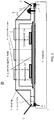
- Fig. 1 illustrates a conventional power module device, shown as module 10, that includes a housing 1, a substrate 3, where in various embodiments the substrate 3 can have upper and lower surfaces being disposed in the housing 1, and upper and lower metallizations respectively disposed on the upper and lower surfaces of the substrate 3.
- the housing 1 can be composed on any suitable material, including but not limited to epoxy, plastic, rubber, silicone, or similar materials.
- the substrate can be composed of any materials suitable for direct copper bonding (DCB) and/or direct aluminum bonding (DAB).
- the substrate 3 is mounted to a heatsink 5, where the heatsink 5 may be composed of any suitable material associated with conventional power modules.
- the housing 1 has formations with holes, e.g.
- the housing 1 has one or more power terminals 4 in relation to the upper surface thereof, where the power terminals 4 can be installed using any suitable methodology associated with conventional power modules.
- the one or more power terminals 4 can have screw holes (not shown), to be connected to exterior busbars (not shown), and dependent on the module application.
- a thermal interface material 6, such as thermal grease, one or more thermal pads or a phase change material (PCM) can be at an interface between heatsink 5 and substrate 3.
- Various electrical components (not shown), e.g. thyristors, diodes, etc. an be contained in the housing 1 or otherwise associated with the module 10.
- At least one embodiment includes a power semiconductor device module.
- the at least one power semiconductor device module includes: a housing in contact with a substrate, a heatsink and a plurality of power terminals, where the housing includes a first tab and a first protrusion, extending substantially perpendicular to one another, and where the first protrusion contacts the heatsink and the first tab contacts the substrate.
- the at least one power semiconductor device module includes: a housing in contact with a substrate, a heatsink and a plurality of power terminals, where the housing includes a first tab and a first protrusion, substantially perpendicular to one another, and where the first protrusion contacts the heatsink and the first tab contacts the substrate, where the first protrusion is a heel.
- the at least one power semiconductor device module includes: a power terminal at least partially contained in a housing, where the power terminal contacts a substrate , where the housing includes a tab and a first protrusion, substantially perpendicular to one another, and where the first tab partially protrudes to an exterior portion of the housing, where the at least first protrusion contacts the heatsink, and the first tab contacts the housing.
- the first protrusion is a heel.
- the at least one power semiconductor device module includes: a power terminal at least partially contained in a housing, where the power terminal contacts a substrate, where the housing includes a first tab and a first protrusion, substantially perpendicular to one another, and where the first tab partially protrudes to an exterior portion of the housing, where the first protrusion contacts the heatsink, and where the first tab contacts the housing.
- the first protrusion is a heel, and where the plurality of power terminals are associated with an exterior portion of the housing.
- the at least one power semiconductor device module includes: a power terminal at least partially contained in a housing, where the power terminal contacts a substrate, where the housing includes a first protrusion and a first tab, substantially perpendicular to one another, and where the first tab partially protrudes to an exterior portion of the housing, where the first protrusion contacts the heatsink, and the first tab contacts the housing.
- the first protrusion is a heel, where the plurality of power terminals are associated with an exterior portion of the housing, and where the substrate is associated with an interior portion of the housing.
- the at least one power semiconductor device module includes: a power terminal at least partially contained in a housing, where the power terminal contacts substrate, where the housing includes a first tab and a first protrusion, substantially perpendicular to one another, and where the first tab partially protrudes to an exterior portion of the housing, where the first protrusion contacts the heatsink, and where the first tab contacts the housing.
- the first protrusion is a heel, where the plurality of power terminals are associated with an exterior portion of the housing, where the substrate is associated with an interior portion of the housing, and where a first screw connected through the first tab to the heatsink.
- the at least one power semiconductor device module includes: a power terminal at least partially contained in a housing, where the power terminal contacts a substrate, where the housing includes a first tab and a first protrusion, substantially perpendicular to one another, and where the first protrusion partially protrudes to an exterior portion of the housing, where the first protrusion contacts the heatsink, and where the first tab parts contacts the housing.
- the first protrusion is a heel, where the plurality of power terminals are associated with an exterior portion of the housing, where the substrate is associated with an interior portion of the housing, and where a first screw connected through the first tab connecting the first tab to the heatsink, and where the housing includes a second tab.
- the at least one power semiconductor device module includes: a power terminal at least partially contained in a housing, where the power terminal contacts a substrate, where the housing includes a first tab and a first protrusion, substantially perpendicular to one another, and where the first tab partially protrudes to an exterior portion of the housing, where the first protrusion contacts the heatsink, and where the first tab contacts the housing.
- the first protrusion is a heel
- the plurality of power terminals are associated with an exterior portion of the housing
- the substrate is associated with an interior portion of the housing
- a first screw connected through the first tab to the heatsink where the housing includes a second tab.
- the second tab is connected to an opposite portion of the housing in relation to the first tab.
- the at least one power semiconductor device module includes: a power terminal at least partially contained in a housing, where the power terminal contacts a substrate, where the housing includes a first tab and a first protrusion with at least two parts, substantially perpendicular to one another, and where the first tab partially protrudes to an exterior portion of the housing, where the first protrusion contacts the heatsink, and where the first tab contacts the housing.
- the first protrusion is a heel
- the plurality of power terminals are associated with an exterior portion of the housing
- the substrate is associated with an interior portion of the housing
- the housing includes a second tab, where the second tab is connected to an opposite portion of the housing in relation to the first tab, and where the second tab is connected to a second protrusion.
- the at least one power semiconductor device module includes: a power terminal at least partially contained in a housing, where the power terminal contacts a substrate, where the housing includes a first tab and a first protrusion, substantially perpendicular to one another, and where the first tab partially protrudes to an exterior portion of the housing, where the first protrusion contacts the heatsink, and where the first tab contacts the housing.
- the first protrusion is a heel
- the plurality of power terminals are associated with an exterior portion of the housing
- the substrate is associated with an interior portion of the housing
- a first screw connects the first tab to the heatsink
- the housing includes a second tab
- the tab protrusion is connected to an opposite portion of the housing in relation to the first tab
- the second tab is connected to a second protrusion, substantially perpendicular in relation to one another.
- the at least one power semiconductor device module includes: a power terminal at least partially contained in a housing, where the power terminal contacts a substrate, where the housing includes a first tab and a first protrusion, substantially perpendicular to one another, and where the first tab partially protrudes to an exterior portion of the housing, where the first protrusion contacts the heatsink, and where the first tab parts contacts the housing.
- the first protrusion is a heel
- the plurality of power terminals are associated with an exterior portion of the housing
- the substrate is associated with an interior portion of the housing
- a first screw connects the first tab to the heatsink
- the housing includes a second tab, where the second tab is connected to an opposite portion of the housing in relation to the first tab, where the second tab is connected to a second protrusion, substantially perpendicular in relation to one another, and where the second protrusion is a heel.
- the at least one power semiconductor device module includes: a power terminal at least partially contained in a housing, where the power terminal contacts a substrate, where the housing includes a first tab and a first protrusion, substantially perpendicular to one another, and where the first tab partially protrudes to an exterior portion of the housing, where the first protrusion contacts the heatsink, and where the first tab contacts the housing.
- the first protrusion is a heel
- the plurality of power terminals are associated with an exterior portion of the housing
- the substrate is associated with an interior portion of the housing
- the housing includes a second tab, where the second tab is connected to an opposite portion of the housing in relation to the first tab, where the second tab is connected to a second protrusion, where substantially perpendicular in relation to one another, where the second protrusion is a heel, and where the second protrusion contacts the heatsink.
- the at least one power semiconductor device module includes: a power terminal at least partially contained in a housing, where the power terminal contacts a substrate, where the housing includes a first tab and a first protrusion, substantially perpendicular to one another, and where the first tab partially protrudes to an exterior portion of the housing, where the first protrusion contacts the heatsink, and where the first tab parts contacts the housing.
- the first protrusion is a heel
- the plurality of power terminals are associated with an exterior portion of the housing
- the substrate is associated with an interior portion of the housing
- the housing includes a second tab
- the second tab is connected to an opposite portion of the housing in relation to the first tab
- the second tab is connected to a second protrusion, where substantially perpendicular in relation to one another
- the second protrusion is a heel
- the second protrusion contacts the heatsink
- the second tab contacts the substrate.
- the at least one power semiconductor device module includes: a power terminal at least partially contained in a housing, where the power terminal contacts a substrate, where the housing includes a first tab and a first protrusion, substantially perpendicular to one another, and where the first tab partially protrudes to an exterior portion of the housing, where the first protrusion contacts the heatsink, and where the first tab contacts the housing.
- the first protrusion is a heel
- the plurality of power terminals are associated with an exterior portion of the housing
- the substrate is associated with an interior portion of the housing, and where a first screw connected through the first tab to the heatsink
- the housing includes a second tab, where the second tab is connected to an opposite portion of the housing in relation to the first tab, where the second tab is connected to a second protrusion, substantially perpendicular in relation to one another, where the second protrusion is a heel, where the second protrusion contacts the heatsink, and where the second tab contacts the substrate, and where a second screw connected through the second tab connects the second tab to the heatsink.
- Yet another embodiment includes a method for configuring a power semiconductor device.
- the method can include: providing a housing with a first tab and a first protrusion, where the first protrusion is in contact with a heatsink and utilizing a first screw to connect the first tab to the heatsink, where the first tab and first protrusion extend substantially perpendicular to one another.
- Yet another embodiment includes a method for configuring a power semiconductor device.
- the method can include: providing a housing with a first tab and a first protrusion, where the first protrusion is in contact with a heatsink, utilizing a first screw to connect the first tab a substrate disposed on the heatsink and the first protrusion to the heatsink, where the method can further include: utilizing a second screw to connect a second tab to the substrate, and a second protrusion to the heatsink, second tab and second protrusion extend substantially perpendicular to one another.
- the terms “on,” “overlying,” “disposed on” and “over” may be used in the following description and claims. “On,” “overlying,” “disposed on” and “over” may be used to indicate that two or more elements are in direct physical contact with one another. Also, the term “on,”, “overlying,” “disposed on,” and “over”, may mean that two or more elements are not in direct contact with one another. For example, “over” may mean that one element is above another element while not contacting one another and may have another element or elements in between the two elements.
- the module 10 pursuant to FIG. 1 suffers from several defects.
- the resulting counterclockwise torque e.g. in relation to the left side of the module 10
- the thermal interface material 6 is a thermal grease or thermal foil placed at the bottom side of the module 10, e.g. at an interface in relation to the heatsink 5, tilting takes place, when a screw is tightened.
- the thermal interface material is displaced, moving out of an advantageous position in relation to the overall module 10.
- the same defect can happen with respect to the right side of the module 10, e.g. clockwise torque causes the displacement if the screw-down starts on the right side of the housing 1.
- the substrate 3 is connected (e.g. soldered) to a baseplate (not shown), in contact to the heatsink 5 after screwing procedures, a similar displacement can occur, and in embodiments where the substrate 3 is a DCB substrate, the local pressure peak to the DCB can cause the substrate 3 to break, resulting in insulating failure.
- One or more embodiments of the present disclosure are directed to remedying the displacement issues and other defects described herein in relation to power modules and housings, in addition to improving the connection of a power module and power module housing in relation to other components and surfaces associated therewith, including the connection of the power module housing to a heatsink.
- one or more protrusions extend at least partially outward in relation to the overall housing and in relation to the screwing positions where the housing will be affixed to a heatsink and connect the housing to the heatsink.
- the protrusions are a bar shape, where in various embodiments the bar shape is a heel shape; (however, this shape is given just as an example and other shapes could be used).
- the one or more protrusions can contain at least two portions (e.g. sub-portions) substantially perpendicular to one another forming a right-angle formation that affixes the housing to the heatsink.
- a hole associated with each of the one or more protrusions can be used to insert a screw therein, thus affixing the protrusions, and by extension the housing, to the heatsink.
- this arrangement improves the mechanical stability of the power module housing (and by extension the overall power module) by reducing the tilting and other displacement effects associated with normal operation and/or other use of the device.
- the increased stability also results in enhanced thermal transfer, in addition to improved pressure contact, between the power module housing (and by extension the overall power module) in relation to the heatsink.
- FIG. 2 illustrates a side cross-sectional view of a power module device 20 in accordance with at least one embodiment of the present disclosure.
- the power module device 20 includes a housing 1 in contact with a heatsink 5 with one or more power terminals 4 extending into and out of the housing 1 and in contact with the substrate 3.
- the housing 1 can be any suitable plastic or other material suitable for housing in power module devices, including but not limited to an injection mold plastic.
- a metal baseplate may be used and may form any suitable connection with the heatsink 5 such that the heatsink 5 is beneath the metal baseplate. Any suitable method of connection between the baseplate and the heatsink can be used, and any suitable material for the baseplate may be used.
- the heatsink 5 can be made of a thermally conductive material, such as a metal.
- the one or more power terminals 4 can have screw holes (not shown), to be connected to exterior busbars (not shown), e.g. as dependent on the module application.
- the one or more power terminals 4 can be of any suitable material and of any suitable type, including but not limited to press-fit terminals and/or solderable terminals, and can be affixed to the power module device 20 using any suitable method.
- the power module device 20 includes a substrate 3 that is mounted to the heatsink 5 using any suitable method in relation thereto, as may be described herein or may otherwise be suitable.
- the housing 1 may include support portions 9, as well as extensions, shown as tabs 7, which extensions extend from a central portion 1A of the housing 1, and provide screw holes 2, for affixing the housing 1 to the heat sink 5.
- the housing 1 may include protrusions 8, extending below the tabs 7, generally perpendicular to the plane of the tabs 7.
- the protrusions 8 are heel shaped, and in various embodiments, the heel shape is a bar forming a connection in relation to the housing 1 and/or the heatsink 5.
- one or more of the protrusions 8 form a contiguous connection with respect to the housing 1, e.g. such that the protrusion portions and/or overall protrusions are actually part of the overall housing of housing 1 and/or part of the molding process utilized to form the same.
- the protrusions 8 are not part of the housing 1, but rather are formed of material or materials physically coupled to the housing.
- the composition of the protrusions 8 can be any suitable rigid materials and combination of materials and may be physically coupled to the housing 1.
- the protrusions 8 are in a bottom portion of the housing 1 such that the overall protrusions contact the heatsink 5.
- the protrusions 8 may extend, partially, into the housing 1 and contact one or more components contained therein.
- the tabs 7 may extend, partially, into the housing and contact the substrate 3 for additional support.
- one or more protrusion portions of protrusions 8 are the same height as all or a portion of the substrate 3, e.g. the DCB and/or DAB exposure.
- FIG. 2B illustrates an embodiment of a power module 20B, arranged generally the same as the embodiment of power module device 20, except having a baseplate 17, disposed on the heatsink 5, so the tabs 7 contact the baseplate 17.
- one or more screws 11 can be employed through one or more screw holes 2 to affix one or more of the tabs 7 to the heatsink 5.
- the screws 11 can be substituted for using another known fastener, and the support of one or more of the tabs 7 can be used.
- the one or more tabs 7 can include a screw hole 2 such that the screw or screws 11 goes through the screw hole 2 and affix the tabs 7 to the heatsink 5, which fixing by extension affixes the entirety of the housing 1 to the heatsink 5.
- the screw 11 goes through a screw hole 2, where the screw hole(s) 2 may be positioned at different locations within the tabs 7, as further detailed in the embodiments of FIGs. 4A-4G .
- the one or more screws 11 can be made from any solid material including, but not limited to, metal, plastic, and other nonmetallic materials. In various embodiments, the one or more screws 11 can be made from insulating or non-insulating material. In various embodiments, material (such as thermal conductive material), may additionally be used for physically coupling the heatsink 5 to the module bottom side (substrate or baseplate).
- various electrical components 15, e.g. thyristors, diodes, etc. an be contained in the housing 1 or otherwise associated with the power module device 20.
- FIG. 3 illustrates a method 30 for affixing a housing of a power module device to a heatsink in accordance with at least one embodiment of the present disclosure.
- the method includes providing a housing with a first tab, where the first tab can be at least partially extending outwardly from the housing and in contact with a heatsink (35).
- the method can further include utilizing a first screw to connect the first tab to the heatsink by inserting a screw through a hole associated with the first tab, where the first tab includes at least two parts each substantially perpendicular to one another, and where one of the at least two parts is associated with the hole and another one of the at least two parts contacts the heatsink (40).
- the shape of the first tab in relation to the housing, and in conjunction with the affixing of the protrusion to the heatsink enhances the mechanical and thermal-transfer stability of the power module.
- a heel or protrusion may be arranged in contact with the first tab, or as an integral portion of the first tab. The protrusion may extend from a lower side of the first tab between the main plane of the first tab and the heatsink.
- the method can further include utilizing a second screw to connect a second tab to the heatsink, where the second tab extends at least partially outside of the housing and in contact with a heatsink, where the second tab includes a first part and a second part each substantially perpendicular to one another, and where the first part of the second tab is associated with the hole facilitating affixation with the second screw and the second part of the second tab contacts the heatsink (45).
- the second part of the tab may be a heel or protrusion. The second screw can be inserted through a hole associated with the first part of the second tab.
- the affixing of the second tab with the second screw further enhances the mechanical and thermal-transfer stability of the power module device by securing the opposite end of the housing, which is already secured at the other end by the first tab and the first screw, thus further reducing mechanical instability and enhancing thermal-transfer properties associated with the power module device.
- FIGs. 4A-4F illustrate variants of the housing 1 according to additional embodiments of the disclosure.
- FIG. 4A a side view is shown of the housing 1, showing general features, including the tabs 7, extending from opposite sides of the central portion 1A of housing 1.
- protrusions 8 are located at a distal end of tabs 7, outside of screw holes 2, and extend downwardly from the lower surface 7A of the tabs 7.
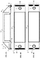
- FIG. 4G depicts a perspective view of the housing 1.
- FIGs. 4B-4F depict a bottom plan view of variants of the housing 1, where the different embodiments may differ from one another in the configuration of the protrusions 8 and screw holes 2, for example.
- the protrusions 8B are arranged as elongated stripes, located at distal ends of the tabs 7, and extending along substantially an entirety of the width of the housing 1B. This configuration may supply protection against torque tending to bend or rotate the housing when the tabs 7 are affixed to a subjacent heatsink (not shown).
- the protrusions 8C are arranged as two separate stripes, located at distal ends of the tabs 7, and extending partially along the width of the housing 1C.
- the omission of material in the middle between the separate stripes may not substantially affect the resistance to any torque or deformation generated when the tabs 7 are affixed to a heat sink.
- a single screw hole 2 is located in each of tabs 7, generally in a central location, to generate symmetrical forces within the tabs 7.
- the housing 1D includes protrusions 8B that are arranged as elongated stripes, generally as described with respect to FIG. 4B .
- two screw holes 2 are located in each of tabs 7, generally in a middle location of a tab 7, to generate symmetrical forces within the tabs 7. The provision of two screw holes may more uniformly distribute forces within the tabs 7, and in a less concentrated manner than with the use of a single screw hole.
- the protrusions 8E of housing 1E are arranged as three separate segments, located at distal ends of the tabs 7, and extending partially along the width of the housing 1E.
- the omission of material in the between the separate segments may not substantially affect the resistance to any torque or deformation generated when the tabs 7 are affixed to a heat sink.
- a single screw hole 2 is located in each of tabs 7, generally in a central location, to generate symmetrical forces within the tabs 7.
- the protrusions 8F of housing IF are arranged as three separate segments, located at distal ends of the tabs 7, and extending partially along the width of the housing IF, and partially along the length of the housing IF.
- the omission of material in the between the separate segments may not substantially affect the resistance to any torque or deformation generated when the tabs 7 are affixed to a heat sink.
- the provision of material extending along the length of the housing IF may also add stability against torque two different directions.
- a single screw hole 2 is located in each of tabs 7, generally in a central location, to generate symmetrical forces within the tabs 7.
Landscapes
- Engineering & Computer Science (AREA)
- Microelectronics & Electronic Packaging (AREA)
- Manufacturing & Machinery (AREA)
- Cooling Or The Like Of Semiconductors Or Solid State Devices (AREA)
- Cooling Or The Like Of Electrical Apparatus (AREA)
Abstract
Description
- Embodiments relate to the field of semiconductor devices, and in particular, protrusion useful in semiconductor packaging.
- Most power semiconductor devices like silicon-controlled rectifiers ("SCRs"), power transistors, insulated gate-bipolar transistors ("IGBTs"), metal-oxide-semiconductor field effect transistors ("MOSFETs"), bipolar power rectifiers, power regulators, or combinations thereof, are assembled in packages that fail to provide sufficient mechanical support or optimal thermal transfer capacities.
-
Fig. 1 illustrates a conventional power module device, shown asmodule 10, that includes ahousing 1, asubstrate 3, where in various embodiments thesubstrate 3 can have upper and lower surfaces being disposed in thehousing 1, and upper and lower metallizations respectively disposed on the upper and lower surfaces of thesubstrate 3. In various embodiments, thehousing 1 can be composed on any suitable material, including but not limited to epoxy, plastic, rubber, silicone, or similar materials. In various embodiments, the substrate can be composed of any materials suitable for direct copper bonding (DCB) and/or direct aluminum bonding (DAB). In various embodiments, thesubstrate 3 is mounted to aheatsink 5, where theheatsink 5 may be composed of any suitable material associated with conventional power modules. In various embodiments, thehousing 1 has formations with holes,e.g. hole 2, for screws to fasten themodule 10 on theheatsink 5. Thehousing 1 has one ormore power terminals 4 in relation to the upper surface thereof, where thepower terminals 4 can be installed using any suitable methodology associated with conventional power modules. In various embodiments, the one ormore power terminals 4 can have screw holes (not shown), to be connected to exterior busbars (not shown), and dependent on the module application. In various embodiments, athermal interface material 6, such as thermal grease, one or more thermal pads or a phase change material (PCM) can be at an interface betweenheatsink 5 andsubstrate 3. Various electrical components (not shown), e.g. thyristors, diodes, etc. an be contained in thehousing 1 or otherwise associated with themodule 10. - In view of the above, the present embodiments are provided.
- At least one embodiment includes a power semiconductor device module. The at least one power semiconductor device module includes: a housing in contact with a substrate, a heatsink and a plurality of power terminals, where the housing includes a first tab and a first protrusion, extending substantially perpendicular to one another, and where the first protrusion contacts the heatsink and the first tab contacts the substrate.
- Another one embodiment includes a power semiconductor device module. The at least one power semiconductor device module includes: a housing in contact with a substrate, a heatsink and a plurality of power terminals, where the housing includes a first tab and a first protrusion, substantially perpendicular to one another, and where the first protrusion contacts the heatsink and the first tab contacts the substrate, where the first protrusion is a heel.
- Yet another one embodiment includes a power semiconductor device module. The at least one power semiconductor device module includes: a power terminal at least partially contained in a housing, where the power terminal contacts a substrate , where the housing includes a tab and a first protrusion, substantially perpendicular to one another, and where the first tab partially protrudes to an exterior portion of the housing, where the at least first protrusion contacts the heatsink, and the first tab contacts the housing. In various embodiments, the first protrusion is a heel.
- Yet another one embodiment includes a power semiconductor device module. The at least one power semiconductor device module includes: a power terminal at least partially contained in a housing, where the power terminal contacts a substrate, where the housing includes a first tab and a first protrusion, substantially perpendicular to one another, and where the first tab partially protrudes to an exterior portion of the housing, where the first protrusion contacts the heatsink, and where the first tab contacts the housing. In various embodiments, the first protrusion is a heel, and where the plurality of power terminals are associated with an exterior portion of the housing.
- Yet another one embodiment includes a power semiconductor device module. The at least one power semiconductor device module includes: a power terminal at least partially contained in a housing, where the power terminal contacts a substrate, where the housing includes a first protrusion and a first tab, substantially perpendicular to one another, and where the first tab partially protrudes to an exterior portion of the housing, where the first protrusion contacts the heatsink, and the first tab contacts the housing. In various embodiments, the first protrusion is a heel, where the plurality of power terminals are associated with an exterior portion of the housing, and where the substrate is associated with an interior portion of the housing.
- Yet another one embodiment includes a power semiconductor device module. The at least one power semiconductor device module includes: a power terminal at least partially contained in a housing, where the power terminal contacts substrate, where the housing includes a first tab and a first protrusion, substantially perpendicular to one another, and where the first tab partially protrudes to an exterior portion of the housing, where the first protrusion contacts the heatsink, and where the first tab contacts the housing. In various embodiments, the first protrusion is a heel, where the plurality of power terminals are associated with an exterior portion of the housing, where the substrate is associated with an interior portion of the housing, and where a first screw connected through the first tab to the heatsink.
- Yet another one embodiment includes a power semiconductor device module. The at least one power semiconductor device module includes: a power terminal at least partially contained in a housing, where the power terminal contacts a substrate, where the housing includes a first tab and a first protrusion, substantially perpendicular to one another, and where the first protrusion partially protrudes to an exterior portion of the housing, where the first protrusion contacts the heatsink, and where the first tab parts contacts the housing. In various embodiments, the first protrusion is a heel, where the plurality of power terminals are associated with an exterior portion of the housing, where the substrate is associated with an interior portion of the housing, and where a first screw connected through the first tab connecting the first tab to the heatsink, and where the housing includes a second tab.
- Yet another one embodiment includes a power semiconductor device module. The at least one power semiconductor device module includes: a power terminal at least partially contained in a housing, where the power terminal contacts a substrate, where the housing includes a first tab and a first protrusion, substantially perpendicular to one another, and where the first tab partially protrudes to an exterior portion of the housing, where the first protrusion contacts the heatsink, and where the first tab contacts the housing. In various embodiments, the first protrusion is a heel, where the plurality of power terminals are associated with an exterior portion of the housing, where the substrate is associated with an interior portion of the housing, and where a first screw connected through the first tab to the heatsink, where the housing includes a second tab., and where the second tab is connected to an opposite portion of the housing in relation to the first tab.
- Yet another one embodiment includes a power semiconductor device module. The at least one power semiconductor device module includes: a power terminal at least partially contained in a housing, where the power terminal contacts a substrate, where the housing includes a first tab and a first protrusion with at least two parts, substantially perpendicular to one another, and where the first tab partially protrudes to an exterior portion of the housing, where the first protrusion contacts the heatsink, and where the first tab contacts the housing. In various embodiments, the first protrusion is a heel, where the plurality of power terminals are associated with an exterior portion of the housing, where the substrate is associated with an interior portion of the housing, and where a first screw connected through the first tab to the heatsink, where the housing includes a second tab, where the second tab is connected to an opposite portion of the housing in relation to the first tab, and where the second tab is connected to a second protrusion.
- Yet another one embodiment includes a power semiconductor device module. The at least one power semiconductor device module includes: a power terminal at least partially contained in a housing, where the power terminal contacts a substrate, where the housing includes a first tab and a first protrusion, substantially perpendicular to one another, and where the first tab partially protrudes to an exterior portion of the housing, where the first protrusion contacts the heatsink, and where the first tab contacts the housing. In various embodiments, the first protrusion is a heel, where the plurality of power terminals are associated with an exterior portion of the housing, where the substrate is associated with an interior portion of the housing, and where a first screw connects the first tab to the heatsink, where the housing includes a second tab, where the tab protrusion is connected to an opposite portion of the housing in relation to the first tab, where the second tab is connected to a second protrusion, substantially perpendicular in relation to one another.
- Yet another one embodiment includes a power semiconductor device module. The at least one power semiconductor device module includes: a power terminal at least partially contained in a housing, where the power terminal contacts a substrate, where the housing includes a first tab and a first protrusion, substantially perpendicular to one another, and where the first tab partially protrudes to an exterior portion of the housing, where the first protrusion contacts the heatsink, and where the first tab parts contacts the housing. In various embodiments, the first protrusion is a heel, where the plurality of power terminals are associated with an exterior portion of the housing, where the substrate is associated with an interior portion of the housing, and where a first screw connects the first tab to the heatsink, where the housing includes a second tab, where the second tab is connected to an opposite portion of the housing in relation to the first tab, where the second tab is connected to a second protrusion, substantially perpendicular in relation to one another, and where the second protrusion is a heel.
- Yet another one embodiment includes a power semiconductor device module. The at least one power semiconductor device module includes: a power terminal at least partially contained in a housing, where the power terminal contacts a substrate, where the housing includes a first tab and a first protrusion, substantially perpendicular to one another, and where the first tab partially protrudes to an exterior portion of the housing, where the first protrusion contacts the heatsink, and where the first tab contacts the housing. In various embodiments, the first protrusion is a heel, where the plurality of power terminals are associated with an exterior portion of the housing, where the substrate is associated with an interior portion of the housing, and where a first screw connected through the first tab to the heatsink, where the housing includes a second tab, where the second tab is connected to an opposite portion of the housing in relation to the first tab, where the second tab is connected to a second protrusion, where substantially perpendicular in relation to one another, where the second protrusion is a heel, and where the second protrusion contacts the heatsink.
- Yet another one embodiment includes a power semiconductor device module. The at least one power semiconductor device module includes: a power terminal at least partially contained in a housing, where the power terminal contacts a substrate, where the housing includes a first tab and a first protrusion, substantially perpendicular to one another, and where the first tab partially protrudes to an exterior portion of the housing, where the first protrusion contacts the heatsink, and where the first tab parts contacts the housing. In various embodiments, the first protrusion is a heel, where the plurality of power terminals are associated with an exterior portion of the housing, where the substrate is associated with an interior portion of the housing, and where a first screw connected through the first tab to the heatsink, where the housing includes a second tab, where the second tab is connected to an opposite portion of the housing in relation to the first tab, where the second tab is connected to a second protrusion, where substantially perpendicular in relation to one another, where the second protrusion is a heel, where the second protrusion contacts the heatsink, and where the second tab contacts the substrate.
- Yet another one embodiment includes a power semiconductor device module. The at least one power semiconductor device module includes: a power terminal at least partially contained in a housing, where the power terminal contacts a substrate, where the housing includes a first tab and a first protrusion, substantially perpendicular to one another, and where the first tab partially protrudes to an exterior portion of the housing, where the first protrusion contacts the heatsink, and where the first tab contacts the housing. In various embodiments, the first protrusion is a heel, where the plurality of power terminals are associated with an exterior portion of the housing, where the substrate is associated with an interior portion of the housing, and where a first screw connected through the first tab to the heatsink, where the housing includes a second tab, where the second tab is connected to an opposite portion of the housing in relation to the first tab, where the second tab is connected to a second protrusion, substantially perpendicular in relation to one another, where the second protrusion is a heel, where the second protrusion contacts the heatsink, and where the second tab contacts the substrate, and where a second screw connected through the second tab connects the second tab to the heatsink.
- Yet another embodiment includes a method for configuring a power semiconductor device. The method can include: providing a housing with a first tab and a first protrusion, where the first protrusion is in contact with a heatsink and utilizing a first screw to connect the first tab to the heatsink, where the first tab and first protrusion extend substantially perpendicular to one another.
- Yet another embodiment includes a method for configuring a power semiconductor device. The method can include: providing a housing with a first tab and a first protrusion, where the first protrusion is in contact with a heatsink, utilizing a first screw to connect the first tab a substrate disposed on the heatsink and the first protrusion to the heatsink, where the method can further include: utilizing a second screw to connect a second tab to the substrate, and a second protrusion to the heatsink, second tab and second protrusion extend substantially perpendicular to one another.
-
-
FIG. 1 shows a schematic of a conventional power semiconductor device module; -
FIG. 2 shows a schematic of a power semiconductor device module according to at least one embodiment of the present disclosure; -
FIG. 2B shows a schematic of another power semiconductor device module according to at least one embodiment of the present disclosure; -
FIG.3 shows a method for affixing a protrusion to a housing and heatsink associated with a power semiconductor device module and according to at least one embodiment of the present disclosure. -
FIGs. 4A-4F illustrate variants of a housing according to additional embodiments of the disclosure. -
FIG. 4G illustrates a perspective view of a housing according to additional embodiments of the disclosure. - The present embodiments will now be described more fully hereinafter with reference to the accompanying drawings, in which exemplary embodiments are shown. The embodiments are not to be construed as limited to the embodiments set forth herein. Rather, these embodiments are provided so that this disclosure will be thorough and complete, and will fully convey their scope to those skilled in the art. In the drawings, like numbers refer to like elements throughout.
- In the following description and/or claims, the terms "on," "overlying," "disposed on" and "over" may be used in the following description and claims. "On," "overlying," "disposed on" and "over" may be used to indicate that two or more elements are in direct physical contact with one another. Also, the term "on,", "overlying," "disposed on," and "over", may mean that two or more elements are not in direct contact with one another. For example, "over" may mean that one element is above another element while not contacting one another and may have another element or elements in between the two elements. Furthermore, the term "and/or" may mean "and", it may mean "or", it may mean "exclusive-or", it may mean "one", it may mean "some, but not all", it may mean "neither", and/or it may mean "both", although the scope of claimed subject matter is not limited in this respect.
- The
module 10 pursuant toFIG. 1 suffers from several defects. In embodiments, where themodule 10 and associatedhousing 1 are screwed down to theheatsink 5, e.g. through one ormore holes 2, the resulting counterclockwise torque (e.g. in relation to the left side of the module 10) can cause a tilting of themodule 10 andhousing 1, and in embodiments where thethermal interface material 6 is a thermal grease or thermal foil placed at the bottom side of themodule 10, e.g. at an interface in relation to theheatsink 5, tilting takes place, when a screw is tightened. As a result, the thermal interface material is displaced, moving out of an advantageous position in relation to theoverall module 10. In various embodiments, the same defect can happen with respect to the right side of themodule 10, e.g. clockwise torque causes the displacement if the screw-down starts on the right side of thehousing 1. - In various embodiments, even if the
substrate 3 is connected (e.g. soldered) to a baseplate (not shown), in contact to theheatsink 5 after screwing procedures, a similar displacement can occur, and in embodiments where thesubstrate 3 is a DCB substrate, the local pressure peak to the DCB can cause thesubstrate 3 to break, resulting in insulating failure. - One or more embodiments of the present disclosure are directed to remedying the displacement issues and other defects described herein in relation to power modules and housings, in addition to improving the connection of a power module and power module housing in relation to other components and surfaces associated therewith, including the connection of the power module housing to a heatsink. In various embodiments, one or more protrusions extend at least partially outward in relation to the overall housing and in relation to the screwing positions where the housing will be affixed to a heatsink and connect the housing to the heatsink. In various embodiments, the protrusions are a bar shape, where in various embodiments the bar shape is a heel shape; (however, this shape is given just as an example and other shapes could be used). The one or more protrusions can contain at least two portions (e.g. sub-portions) substantially perpendicular to one another forming a right-angle formation that affixes the housing to the heatsink. A hole associated with each of the one or more protrusions can be used to insert a screw therein, thus affixing the protrusions, and by extension the housing, to the heatsink. In various embodiments, this arrangement improves the mechanical stability of the power module housing (and by extension the overall power module) by reducing the tilting and other displacement effects associated with normal operation and/or other use of the device. In various embodiments, the increased stability also results in enhanced thermal transfer, in addition to improved pressure contact, between the power module housing (and by extension the overall power module) in relation to the heatsink.
-
FIG. 2 illustrates a side cross-sectional view of apower module device 20 in accordance with at least one embodiment of the present disclosure. In various embodiments, thepower module device 20 includes ahousing 1 in contact with aheatsink 5 with one ormore power terminals 4 extending into and out of thehousing 1 and in contact with thesubstrate 3. In various embodiments, thehousing 1 can be any suitable plastic or other material suitable for housing in power module devices, including but not limited to an injection mold plastic. In various embodiments (not shown), a metal baseplate may be used and may form any suitable connection with theheatsink 5 such that theheatsink 5 is beneath the metal baseplate. Any suitable method of connection between the baseplate and the heatsink can be used, and any suitable material for the baseplate may be used. In various embodiments, theheatsink 5 can be made of a thermally conductive material, such as a metal. In various embodiments, the one ormore power terminals 4 can have screw holes (not shown), to be connected to exterior busbars (not shown), e.g. as dependent on the module application. - In various embodiments, the one or
more power terminals 4 can be of any suitable material and of any suitable type, including but not limited to press-fit terminals and/or solderable terminals, and can be affixed to thepower module device 20 using any suitable method. Thepower module device 20 includes asubstrate 3 that is mounted to theheatsink 5 using any suitable method in relation thereto, as may be described herein or may otherwise be suitable. In various embodiments, thehousing 1 may includesupport portions 9, as well as extensions, shown astabs 7, which extensions extend from acentral portion 1A of thehousing 1, and providescrew holes 2, for affixing thehousing 1 to theheat sink 5. Notably, thehousing 1 may includeprotrusions 8, extending below thetabs 7, generally perpendicular to the plane of thetabs 7. As shown inFIG. 2 , while thecentral portion 1A of thehousing 1 and/or thetabs 7 may contact thesubstrate 3, the protrusions extend to contact the upper surface ofheatsink 5. In various embodiments, theprotrusions 8 are heel shaped, and in various embodiments, the heel shape is a bar forming a connection in relation to thehousing 1 and/or theheatsink 5. In various embodiments, one or more of theprotrusions 8 form a contiguous connection with respect to thehousing 1, e.g. such that the protrusion portions and/or overall protrusions are actually part of the overall housing ofhousing 1 and/or part of the molding process utilized to form the same. In various embodiments, theprotrusions 8 are not part of thehousing 1, but rather are formed of material or materials physically coupled to the housing. In various embodiments, the composition of theprotrusions 8 can be any suitable rigid materials and combination of materials and may be physically coupled to thehousing 1. - In various embodiments, as stated and implied, the
protrusions 8 are in a bottom portion of thehousing 1 such that the overall protrusions contact theheatsink 5. In various embodiments theprotrusions 8 may extend, partially, into thehousing 1 and contact one or more components contained therein. In various embodiment, thetabs 7 may extend, partially, into the housing and contact thesubstrate 3 for additional support. In various embodiments, one or more protrusion portions ofprotrusions 8 are the same height as all or a portion of thesubstrate 3, e.g. the DCB and/or DAB exposure. - In various embodiments, if a baseplate is located between the substrate and the heatsink, then the
protrusions 8 may directly contact the baseplate instead of theheatsink 5; alternatively, the connection to theheatsink 5 may be direct with portions of the baseplate surrounding theprotrusions 8.FIG. 2B illustrates an embodiment of apower module 20B, arranged generally the same as the embodiment ofpower module device 20, except having abaseplate 17, disposed on theheatsink 5, so thetabs 7 contact thebaseplate 17. - In various embodiments, as shown, one or
more screws 11 can be employed through one ormore screw holes 2 to affix one or more of thetabs 7 to theheatsink 5. In various embodiments, thescrews 11 can be substituted for using another known fastener, and the support of one or more of thetabs 7 can be used. The one ormore tabs 7 can include ascrew hole 2 such that the screw or screws 11 goes through thescrew hole 2 and affix thetabs 7 to theheatsink 5, which fixing by extension affixes the entirety of thehousing 1 to theheatsink 5. As shown, thescrew 11 goes through ascrew hole 2, where the screw hole(s) 2 may be positioned at different locations within thetabs 7, as further detailed in the embodiments ofFIGs. 4A-4G . In various embodiments, the one ormore screws 11 can be made from any solid material including, but not limited to, metal, plastic, and other nonmetallic materials. In various embodiments, the one ormore screws 11 can be made from insulating or non-insulating material. In various embodiments, material (such as thermal conductive material), may additionally be used for physically coupling theheatsink 5 to the module bottom side (substrate or baseplate). - In various embodiments, various
electrical components 15, e.g. thyristors, diodes, etc. an be contained in thehousing 1 or otherwise associated with thepower module device 20. -
FIG. 3 illustrates amethod 30 for affixing a housing of a power module device to a heatsink in accordance with at least one embodiment of the present disclosure. The method includes providing a housing with a first tab, where the first tab can be at least partially extending outwardly from the housing and in contact with a heatsink (35). The method can further include utilizing a first screw to connect the first tab to the heatsink by inserting a screw through a hole associated with the first tab, where the first tab includes at least two parts each substantially perpendicular to one another, and where one of the at least two parts is associated with the hole and another one of the at least two parts contacts the heatsink (40). In various embodiments, the shape of the first tab in relation to the housing, and in conjunction with the affixing of the protrusion to the heatsink, enhances the mechanical and thermal-transfer stability of the power module. In various embodiments, a heel or protrusion may be arranged in contact with the first tab, or as an integral portion of the first tab. The protrusion may extend from a lower side of the first tab between the main plane of the first tab and the heatsink. In various embodiments, the method can further include utilizing a second screw to connect a second tab to the heatsink, where the second tab extends at least partially outside of the housing and in contact with a heatsink, where the second tab includes a first part and a second part each substantially perpendicular to one another, and where the first part of the second tab is associated with the hole facilitating affixation with the second screw and the second part of the second tab contacts the heatsink (45). In various embodiments, the second part of the tab may be a heel or protrusion. The second screw can be inserted through a hole associated with the first part of the second tab. The affixing of the second tab with the second screw further enhances the mechanical and thermal-transfer stability of the power module device by securing the opposite end of the housing, which is already secured at the other end by the first tab and the first screw, thus further reducing mechanical instability and enhancing thermal-transfer properties associated with the power module device. -
FIGs. 4A-4F illustrate variants of thehousing 1 according to additional embodiments of the disclosure. InFIG. 4A , a side view is shown of thehousing 1, showing general features, including thetabs 7, extending from opposite sides of thecentral portion 1A ofhousing 1. As shown,protrusions 8 are located at a distal end oftabs 7, outside ofscrew holes 2, and extend downwardly from thelower surface 7A of thetabs 7.FIG. 4G depicts a perspective view of thehousing 1. -
FIGs. 4B-4F depict a bottom plan view of variants of thehousing 1, where the different embodiments may differ from one another in the configuration of theprotrusions 8 and screwholes 2, for example. InFIG. 4B , theprotrusions 8B are arranged as elongated stripes, located at distal ends of thetabs 7, and extending along substantially an entirety of the width of thehousing 1B. This configuration may supply protection against torque tending to bend or rotate the housing when thetabs 7 are affixed to a subjacent heatsink (not shown). - In
FIG. 4C , theprotrusions 8C are arranged as two separate stripes, located at distal ends of thetabs 7, and extending partially along the width of thehousing 1C. The omission of material in the middle between the separate stripes may not substantially affect the resistance to any torque or deformation generated when thetabs 7 are affixed to a heat sink. In both embodiments ofFIG. 4B and FIG. 4C , asingle screw hole 2 is located in each oftabs 7, generally in a central location, to generate symmetrical forces within thetabs 7. - In
FIG. 4D , thehousing 1D includesprotrusions 8B that are arranged as elongated stripes, generally as described with respect toFIG. 4B . In this embodiment, twoscrew holes 2 are located in each oftabs 7, generally in a middle location of atab 7, to generate symmetrical forces within thetabs 7. The provision of two screw holes may more uniformly distribute forces within thetabs 7, and in a less concentrated manner than with the use of a single screw hole. - In
FIG. 4E , the protrusions 8E ofhousing 1E are arranged as three separate segments, located at distal ends of thetabs 7, and extending partially along the width of thehousing 1E. The omission of material in the between the separate segments may not substantially affect the resistance to any torque or deformation generated when thetabs 7 are affixed to a heat sink. In this embodiment asingle screw hole 2 is located in each oftabs 7, generally in a central location, to generate symmetrical forces within thetabs 7. - In
FIG. 4F , theprotrusions 8F of housing IF are arranged as three separate segments, located at distal ends of thetabs 7, and extending partially along the width of the housing IF, and partially along the length of the housing IF. The omission of material in the between the separate segments may not substantially affect the resistance to any torque or deformation generated when thetabs 7 are affixed to a heat sink. The provision of material extending along the length of the housing IF may also add stability against torque two different directions. In this embodiment asingle screw hole 2 is located in each oftabs 7, generally in a central location, to generate symmetrical forces within thetabs 7. - While the present embodiments have been disclosed with reference to certain embodiments, numerous modifications, alterations and changes to the described embodiments are possible while not departing from the sphere and scope of the present disclosure, as defined in the appended claims. Accordingly, the present embodiments are not to be limited to the described embodiments and may have the full scope defined by the language of the following claims, and equivalents thereof.
Claims (15)
- A power semiconductor device module, comprising:
a housing in contact with a substrate, a heatsink and a plurality of power terminals, wherein the housing includes a first tab, and a first protrusion, and wherein the first tab contacts the housing and the first protrusion contacts the heatsink. - The power semiconductor device module of claim 1 with one or more of the following: wherein the first protrusion is a heel;
wherein the plurality of power terminals are associated with an exterior portion of the housing;
wherein the substrate is enclosed by a central portion of the housing. - The power semiconductor device module of claim 1 or 2, further comprising:
a first screw connected extending through a first screw hole in the first tab, and connecting the first tab to the heatsink. - The power semiconductor device module of any of the preceding claims, wherein the first tab extends from a central portion of the housing, wherein the housing includes a second tab, extending from an opposite side of the central portion, preferably further comprising a second screw hole, disposed within the second tab and a second protrusion, extending between the second tab and the heatsink, and/or wherein the second tab and the second protrusion are substantially perpendicular in relation to one another, and/or wherein the second protrusion is a heel.
- The power semiconductor device module of claim 4, further comprising:
a second screw extending through the second screw hole of the second tab, and connecting the second tab to the heatsink. - The power semiconductor device module of claim 4 or 5, wherein the first protrusion and the second protrusion include a plurality of portions.
- The power semiconductor device module of any of the claims 4-6, wherein the first tab and the second tab include a plurality of screw holes.
- The power semiconductor device module of any of the preceding claims 4-7, wherein the first protrusion and the second protrusion are arranged along a distal portion of the first tab and the second tab, respectively, outside of the first screw hole and the second screw hole.
- A method for configuring a power semiconductor device:providing a housing having a central portion, a first tab, extending laterally from the central portion, and a first protrusion, extending subjacent the first tab;arranging the central portion over a substrate, when a heatsink is disposed subjacent the substrate; andconnecting the first tab to the heatsink using a first fastener extending through the first tab, wherein the first protrusion spaces the first tab apart from the heatsink after the connecting.
- The method of claim 9, the housing further comprising a second tab, extending laterally from the central portion on an opposite side from the first tab, and a second protrusion, extending subjacent the second tab, the method further comprising:
connecting the second tab to the heatsink using a second fastener extending through the second tab, wherein the second protrusion spaces the second tab apart from the heatsink after the connecting. - The method of claim 9 or 10, wherein the first tab includes a first screw hole and the second tab includes a second screw hole, wherein the first fastener comprises a first screw, extending through the first screw hole, wherein the second fastener comprises a second screw, extending through the second screw hole.
- The method of claim 11, wherein the first protrusion and the second protrusion are arranged in a distal portion of the first tab and the second tab, respectively, the first protrusion and the second protrusion being outside of the first screw hole and the second screw hole, respectively, with respect to the central portion of the housing.
- A power semiconductor device module, comprising:a heatsink;a substrate, disposed on the heatsink;at least one power semiconductor device, disposed on the substrate; anda housing in contact with the substrate, wherein the housing includes a central portion, a first tab extending laterally from the central portion, and a first protrusion, extending subjacent the first tab,wherein at least one of the central portion and the first tab are disposed in contact with the substrate.
- The power semiconductor device module of claim 13, wherein a baseplate extends under the first tab, and the first tab is spaced apart from the baseplate by the first protrusion.
- The power semiconductor device module of claim 13 or 14, further comprising a second tab extending laterally from the central portion, on a side opposite to the first tab, and a second protrusion, extending subjacent the second tab.
Priority Applications (4)
| Application Number | Priority Date | Filing Date | Title |
|---|---|---|---|
| EP20159811.7A EP3872854A1 (en) | 2020-02-27 | 2020-02-27 | Power module housing with improved protrusion design |
| US17/182,741 US20210272874A1 (en) | 2020-02-27 | 2021-02-23 | Power module housing with improved protrusion design |
| TW110106829A TW202147527A (en) | 2020-02-27 | 2021-02-26 | Power semiconductor device module and method for configuring power semiconductor device |
| CN202110225949.1A CN113314471A (en) | 2020-02-27 | 2021-03-01 | Power module housing with improved protrusion design |
Applications Claiming Priority (1)
| Application Number | Priority Date | Filing Date | Title |
|---|---|---|---|
| EP20159811.7A EP3872854A1 (en) | 2020-02-27 | 2020-02-27 | Power module housing with improved protrusion design |
Publications (1)
| Publication Number | Publication Date |
|---|---|
| EP3872854A1 true EP3872854A1 (en) | 2021-09-01 |
Family
ID=69742778
Family Applications (1)
| Application Number | Title | Priority Date | Filing Date |
|---|---|---|---|
| EP20159811.7A Pending EP3872854A1 (en) | 2020-02-27 | 2020-02-27 | Power module housing with improved protrusion design |
Country Status (4)
| Country | Link |
|---|---|
| US (1) | US20210272874A1 (en) |
| EP (1) | EP3872854A1 (en) |
| CN (1) | CN113314471A (en) |
| TW (1) | TW202147527A (en) |
Cited By (1)
| Publication number | Priority date | Publication date | Assignee | Title |
|---|---|---|---|---|
| EP4307362A1 (en) * | 2022-07-11 | 2024-01-17 | Littelfuse, Inc. | High reliability semiconductor package design |
Families Citing this family (2)
| Publication number | Priority date | Publication date | Assignee | Title |
|---|---|---|---|---|
| US12494596B2 (en) * | 2021-07-28 | 2025-12-09 | Mitsubishi Electric Corporation | Circuit connection device, rotating electric machine device, and method for manufacturing circuit connection device |
| WO2023208348A1 (en) * | 2022-04-28 | 2023-11-02 | Hitachi Energy Switzerland Ag | Semiconductor power module and method for manufacturing a semiconductor power module |
Citations (6)
| Publication number | Priority date | Publication date | Assignee | Title |
|---|---|---|---|---|
| JPH04233752A (en) * | 1990-12-28 | 1992-08-21 | Shinko Electric Ind Co Ltd | Package for electronic component |
| US5981036A (en) * | 1996-04-03 | 1999-11-09 | Schulz-Harder; Juergen | Metal ceramic substrate |
| EP2814056A1 (en) * | 2012-09-13 | 2014-12-17 | Fuji Electric Co., Ltd. | Semiconductor device, method for attaching heat dissipating member to semiconductor device, and method for manufacturing semiconductor device |
| US9929066B1 (en) * | 2016-12-13 | 2018-03-27 | Ixys Corporation | Power semiconductor device module baseplate having peripheral heels |
| US20190074238A1 (en) * | 2017-09-06 | 2019-03-07 | Mitsubishi Electric Corporation | Semiconductor device |
| EP3499563A1 (en) * | 2017-12-13 | 2019-06-19 | SEMIKRON Elektronik GmbH & Co. KG | Semiconductor power module and method for assembling a semiconductor power module in a force-fitting manner |
Family Cites Families (5)
| Publication number | Priority date | Publication date | Assignee | Title |
|---|---|---|---|---|
| JPH0612797B2 (en) * | 1985-09-09 | 1994-02-16 | オムロン株式会社 | Semiconductor device |
| JP3919398B2 (en) * | 1999-10-27 | 2007-05-23 | 三菱電機株式会社 | Semiconductor module |
| JP5061717B2 (en) * | 2007-05-18 | 2012-10-31 | 富士電機株式会社 | Semiconductor module and method for manufacturing semiconductor module |
| EP2998992B1 (en) * | 2011-06-27 | 2019-05-01 | Rohm Co., Ltd. | Semiconductor module |
| JP6237912B2 (en) * | 2014-08-28 | 2017-11-29 | 富士電機株式会社 | Power semiconductor module |
-
2020
- 2020-02-27 EP EP20159811.7A patent/EP3872854A1/en active Pending
-
2021
- 2021-02-23 US US17/182,741 patent/US20210272874A1/en not_active Abandoned
- 2021-02-26 TW TW110106829A patent/TW202147527A/en unknown
- 2021-03-01 CN CN202110225949.1A patent/CN113314471A/en active Pending
Patent Citations (6)
| Publication number | Priority date | Publication date | Assignee | Title |
|---|---|---|---|---|
| JPH04233752A (en) * | 1990-12-28 | 1992-08-21 | Shinko Electric Ind Co Ltd | Package for electronic component |
| US5981036A (en) * | 1996-04-03 | 1999-11-09 | Schulz-Harder; Juergen | Metal ceramic substrate |
| EP2814056A1 (en) * | 2012-09-13 | 2014-12-17 | Fuji Electric Co., Ltd. | Semiconductor device, method for attaching heat dissipating member to semiconductor device, and method for manufacturing semiconductor device |
| US9929066B1 (en) * | 2016-12-13 | 2018-03-27 | Ixys Corporation | Power semiconductor device module baseplate having peripheral heels |
| US20190074238A1 (en) * | 2017-09-06 | 2019-03-07 | Mitsubishi Electric Corporation | Semiconductor device |
| EP3499563A1 (en) * | 2017-12-13 | 2019-06-19 | SEMIKRON Elektronik GmbH & Co. KG | Semiconductor power module and method for assembling a semiconductor power module in a force-fitting manner |
Cited By (1)
| Publication number | Priority date | Publication date | Assignee | Title |
|---|---|---|---|---|
| EP4307362A1 (en) * | 2022-07-11 | 2024-01-17 | Littelfuse, Inc. | High reliability semiconductor package design |
Also Published As
| Publication number | Publication date |
|---|---|
| TW202147527A (en) | 2021-12-16 |
| CN113314471A (en) | 2021-08-27 |
| US20210272874A1 (en) | 2021-09-02 |
Similar Documents
| Publication | Publication Date | Title |
|---|---|---|
| US7440282B2 (en) | Heat sink electronic package having compliant pedestal | |
| KR101444550B1 (en) | Semiconductor module | |
| JP2801534B2 (en) | Power semiconductor module and insulated metal substrate used therefor | |
| KR101477378B1 (en) | Housing and power module having the same | |
| US10978371B2 (en) | Semiconductor device and method for manufacturing semiconductor device | |
| US8648462B2 (en) | Semiconductor power module | |
| US20210272874A1 (en) | Power module housing with improved protrusion design | |
| US6337796B2 (en) | Semiconductor device mount structure having heat dissipating member for dissipating heat generated from semiconductor device | |
| TW452945B (en) | Thermally conductive mounting arrangement for securing an integrated circuit package to a heat sink | |
| EP4148778B1 (en) | Power semiconductor module | |
| US7598600B2 (en) | Stackable power semiconductor package system | |
| CN104066291B (en) | Housing And Power Module Having The Same | |
| US20080158822A1 (en) | Sub-Assembly | |
| US9842786B2 (en) | Semiconductor device | |
| US11211304B2 (en) | Assembly and method for mounting an electronic component to a substrate | |
| US4471407A (en) | Combination heat sink for a semiconductor | |
| JP2002198477A (en) | Semiconductor device | |
| CN100373600C (en) | heat sink | |
| US6351385B1 (en) | Heat sink for integrated circuit packages | |
| JP2001284524A (en) | Power semiconductor module | |
| US5391919A (en) | Semiconductor power module with identical mounting frames | |
| US11201101B2 (en) | Electronic component | |
| US20230197561A1 (en) | Power semiconductor module comprising a substrate, power semiconductor components and comprising a pressure body | |
| TWI876423B (en) | Semiconductor device package, semiconductor device package assembly and method of fabricating the same | |
| CN116031222A (en) | Semiconductor package with blind via attachment to heat sink |
Legal Events
| Date | Code | Title | Description |
|---|---|---|---|
| PUAI | Public reference made under article 153(3) epc to a published international application that has entered the european phase |
Free format text: ORIGINAL CODE: 0009012 |
|
| STAA | Information on the status of an ep patent application or granted ep patent |
Free format text: STATUS: THE APPLICATION HAS BEEN PUBLISHED |
|
| AK | Designated contracting states |
Kind code of ref document: A1 Designated state(s): AL AT BE BG CH CY CZ DE DK EE ES FI FR GB GR HR HU IE IS IT LI LT LU LV MC MK MT NL NO PL PT RO RS SE SI SK SM TR |
|
| STAA | Information on the status of an ep patent application or granted ep patent |
Free format text: STATUS: REQUEST FOR EXAMINATION WAS MADE |
|
| 17P | Request for examination filed |
Effective date: 20220301 |
|
| RBV | Designated contracting states (corrected) |
Designated state(s): AL AT BE BG CH CY CZ DE DK EE ES FI FR GB GR HR HU IE IS IT LI LT LU LV MC MK MT NL NO PL PT RO RS SE SI SK SM TR |