EP3872533A1 - Photon-counting type radiation detector and radiation examination device using same - Google Patents
Photon-counting type radiation detector and radiation examination device using same Download PDFInfo
- Publication number
- EP3872533A1 EP3872533A1 EP19876970.5A EP19876970A EP3872533A1 EP 3872533 A1 EP3872533 A1 EP 3872533A1 EP 19876970 A EP19876970 A EP 19876970A EP 3872533 A1 EP3872533 A1 EP 3872533A1
- Authority
- EP
- European Patent Office
- Prior art keywords
- substrate
- epitaxial layer
- sub
- radiation detector
- photon counting
- Prior art date
- Legal status (The legal status is an assumption and is not a legal conclusion. Google has not performed a legal analysis and makes no representation as to the accuracy of the status listed.)
- Granted
Links
Images







Classifications
-
- H—ELECTRICITY
- H10—SEMICONDUCTOR DEVICES; ELECTRIC SOLID-STATE DEVICES NOT OTHERWISE PROVIDED FOR
- H10F—INORGANIC SEMICONDUCTOR DEVICES SENSITIVE TO INFRARED RADIATION, LIGHT, ELECTROMAGNETIC RADIATION OF SHORTER WAVELENGTH OR CORPUSCULAR RADIATION
- H10F39/00—Integrated devices, or assemblies of multiple devices, comprising at least one element covered by group H10F30/00, e.g. radiation detectors comprising photodiode arrays
- H10F39/80—Constructional details of image sensors
- H10F39/802—Geometry or disposition of elements in pixels, e.g. address-lines or gate electrodes
- H10F39/8027—Geometry of the photosensitive area
-
- H—ELECTRICITY
- H10—SEMICONDUCTOR DEVICES; ELECTRIC SOLID-STATE DEVICES NOT OTHERWISE PROVIDED FOR
- H10F—INORGANIC SEMICONDUCTOR DEVICES SENSITIVE TO INFRARED RADIATION, LIGHT, ELECTROMAGNETIC RADIATION OF SHORTER WAVELENGTH OR CORPUSCULAR RADIATION
- H10F39/00—Integrated devices, or assemblies of multiple devices, comprising at least one element covered by group H10F30/00, e.g. radiation detectors comprising photodiode arrays
- H10F39/80—Constructional details of image sensors
-
- G—PHYSICS
- G01—MEASURING; TESTING
- G01T—MEASUREMENT OF NUCLEAR OR X-RADIATION
- G01T1/00—Measuring X-radiation, gamma radiation, corpuscular radiation, or cosmic radiation
- G01T1/16—Measuring radiation intensity
- G01T1/24—Measuring radiation intensity with semiconductor detectors
-
- G—PHYSICS
- G01—MEASURING; TESTING
- G01T—MEASUREMENT OF NUCLEAR OR X-RADIATION
- G01T1/00—Measuring X-radiation, gamma radiation, corpuscular radiation, or cosmic radiation
- G01T1/16—Measuring radiation intensity
- G01T1/24—Measuring radiation intensity with semiconductor detectors
- G01T1/241—Electrode arrangements, e.g. continuous or parallel strips or the like
-
- H—ELECTRICITY
- H10—SEMICONDUCTOR DEVICES; ELECTRIC SOLID-STATE DEVICES NOT OTHERWISE PROVIDED FOR
- H10F—INORGANIC SEMICONDUCTOR DEVICES SENSITIVE TO INFRARED RADIATION, LIGHT, ELECTROMAGNETIC RADIATION OF SHORTER WAVELENGTH OR CORPUSCULAR RADIATION
- H10F30/00—Individual radiation-sensitive semiconductor devices in which radiation controls the flow of current through the devices, e.g. photodetectors
- H10F30/20—Individual radiation-sensitive semiconductor devices in which radiation controls the flow of current through the devices, e.g. photodetectors the devices having potential barriers, e.g. phototransistors
- H10F30/29—Individual radiation-sensitive semiconductor devices in which radiation controls the flow of current through the devices, e.g. photodetectors the devices having potential barriers, e.g. phototransistors the devices being sensitive to radiation having very short wavelengths, e.g. X-rays, gamma-rays or corpuscular radiation
-
- H—ELECTRICITY
- H10—SEMICONDUCTOR DEVICES; ELECTRIC SOLID-STATE DEVICES NOT OTHERWISE PROVIDED FOR
- H10F—INORGANIC SEMICONDUCTOR DEVICES SENSITIVE TO INFRARED RADIATION, LIGHT, ELECTROMAGNETIC RADIATION OF SHORTER WAVELENGTH OR CORPUSCULAR RADIATION
- H10F39/00—Integrated devices, or assemblies of multiple devices, comprising at least one element covered by group H10F30/00, e.g. radiation detectors comprising photodiode arrays
- H10F39/10—Integrated devices
- H10F39/12—Image sensors
- H10F39/18—Complementary metal-oxide-semiconductor [CMOS] image sensors; Photodiode array image sensors
- H10F39/189—X-ray, gamma-ray or corpuscular radiation imagers
- H10F39/1892—Direct radiation image sensors
-
- H—ELECTRICITY
- H10—SEMICONDUCTOR DEVICES; ELECTRIC SOLID-STATE DEVICES NOT OTHERWISE PROVIDED FOR
- H10F—INORGANIC SEMICONDUCTOR DEVICES SENSITIVE TO INFRARED RADIATION, LIGHT, ELECTROMAGNETIC RADIATION OF SHORTER WAVELENGTH OR CORPUSCULAR RADIATION
- H10F77/00—Constructional details of devices covered by this subclass
- H10F77/10—Semiconductor bodies
- H10F77/12—Active materials
-
- H—ELECTRICITY
- H10—SEMICONDUCTOR DEVICES; ELECTRIC SOLID-STATE DEVICES NOT OTHERWISE PROVIDED FOR
- H10F—INORGANIC SEMICONDUCTOR DEVICES SENSITIVE TO INFRARED RADIATION, LIGHT, ELECTROMAGNETIC RADIATION OF SHORTER WAVELENGTH OR CORPUSCULAR RADIATION
- H10F77/00—Constructional details of devices covered by this subclass
- H10F77/10—Semiconductor bodies
- H10F77/12—Active materials
- H10F77/122—Active materials comprising only Group IV materials
-
- H—ELECTRICITY
- H10—SEMICONDUCTOR DEVICES; ELECTRIC SOLID-STATE DEVICES NOT OTHERWISE PROVIDED FOR
- H10F—INORGANIC SEMICONDUCTOR DEVICES SENSITIVE TO INFRARED RADIATION, LIGHT, ELECTROMAGNETIC RADIATION OF SHORTER WAVELENGTH OR CORPUSCULAR RADIATION
- H10F77/00—Constructional details of devices covered by this subclass
- H10F77/10—Semiconductor bodies
- H10F77/12—Active materials
- H10F77/122—Active materials comprising only Group IV materials
- H10F77/1226—Active materials comprising only Group IV materials comprising multiple Group IV elements, e.g. SiC
-
- H—ELECTRICITY
- H10—SEMICONDUCTOR DEVICES; ELECTRIC SOLID-STATE DEVICES NOT OTHERWISE PROVIDED FOR
- H10F—INORGANIC SEMICONDUCTOR DEVICES SENSITIVE TO INFRARED RADIATION, LIGHT, ELECTROMAGNETIC RADIATION OF SHORTER WAVELENGTH OR CORPUSCULAR RADIATION
- H10F77/00—Constructional details of devices covered by this subclass
- H10F77/10—Semiconductor bodies
- H10F77/12—Active materials
- H10F77/123—Active materials comprising only Group II-VI materials, e.g. CdS, ZnS or HgCdTe
-
- H—ELECTRICITY
- H10—SEMICONDUCTOR DEVICES; ELECTRIC SOLID-STATE DEVICES NOT OTHERWISE PROVIDED FOR
- H10F—INORGANIC SEMICONDUCTOR DEVICES SENSITIVE TO INFRARED RADIATION, LIGHT, ELECTROMAGNETIC RADIATION OF SHORTER WAVELENGTH OR CORPUSCULAR RADIATION
- H10F77/00—Constructional details of devices covered by this subclass
- H10F77/10—Semiconductor bodies
- H10F77/12—Active materials
- H10F77/124—Active materials comprising only Group III-V materials, e.g. GaAs
-
- H—ELECTRICITY
- H10—SEMICONDUCTOR DEVICES; ELECTRIC SOLID-STATE DEVICES NOT OTHERWISE PROVIDED FOR
- H10F—INORGANIC SEMICONDUCTOR DEVICES SENSITIVE TO INFRARED RADIATION, LIGHT, ELECTROMAGNETIC RADIATION OF SHORTER WAVELENGTH OR CORPUSCULAR RADIATION
- H10F77/00—Constructional details of devices covered by this subclass
- H10F77/10—Semiconductor bodies
- H10F77/12—Active materials
- H10F77/124—Active materials comprising only Group III-V materials, e.g. GaAs
- H10F77/1246—III-V nitrides, e.g. GaN
-
- H—ELECTRICITY
- H10—SEMICONDUCTOR DEVICES; ELECTRIC SOLID-STATE DEVICES NOT OTHERWISE PROVIDED FOR
- H10F—INORGANIC SEMICONDUCTOR DEVICES SENSITIVE TO INFRARED RADIATION, LIGHT, ELECTROMAGNETIC RADIATION OF SHORTER WAVELENGTH OR CORPUSCULAR RADIATION
- H10F77/00—Constructional details of devices covered by this subclass
- H10F77/20—Electrodes
- H10F77/206—Electrodes for devices having potential barriers
Definitions
- One or more embodiments generally relate to a photon counting radiation detector and a radiographic inspection device using the same.
- Radiographic inspection devices are used in various fields as medical devices, industrial non-destructive inspection devices, and the like.
- medical devices include computed tomography (CT) devices and positron emission tomography (PET) devices.
- CT computed tomography
- PET positron emission tomography
- the radiation used may be X-rays, gamma rays, or the like.
- a luminescent material called a solid scintillator is used in X-ray CT devices.
- the solid scintillator is a substance that emits light when irradiated with X-rays.
- An X-ray CT device that uses a solid scintillator converts X-rays passing through a test subject into visible light via the solid scintillator. The visible light is converted into an electrical signal via a photodiode detector to obtain a tomogram.
- this technique has developed to the stage where three-dimensional images can be obtained.
- JP S63-40381A Patent Document 2
- a radiation detector installed with a photon counting radiation detector In a photon counting system, X-ray photons passing through a test subject can be directly converted into an electrical signal. This technology is expected to allow the exposure amount to be reduced and other advantages.
- Patent Document 2 a structure including semiconductor elements disposed inclined with respect to an incident direction of radiation is described.
- this structure at least two of the semiconductor elements are disposed overlapping one another. This alleviates the radiation incident position dependency of the total charge induced at the electrode surface.
- This invention was made in light of the problem described above and provides a photon counting radiation detector capable of obtaining higher resolution images.
- a photon counting radiation detector includes: a cell structure including a substrate, and an epitaxial layer provided on the substrate, radiation being incident on the epitaxial layer; an inclination ⁇ of the substrate satisfying Formula (1) below, where t sub is a thickness of the substrate, t epi is a thickness of the epitaxial layer, L is a length of the substrate, and the inclination ⁇ is an inclination of the substrate with respect to an incident direction of the radiation; 0 ⁇ tan ⁇ ⁇ L ⁇ L 2 ⁇ 4 t sub t sub + t epi 2 t sub + t epi
- a photon counting radiation detector includes an epitaxial layer, allowing the incident surface of radiation to be made small. Also, an inclination ⁇ of the substrate is set within a specific range, allowing for higher resolution of images.
- a photon counting radiation detector includes: a cell structure including a substrate, and an epitaxial layer provided on the substrate, radiation being incident on the epitaxial layer; an inclination ⁇ of the substrate satisfying Formula (1) below, where t sub is a thickness of the substrate, t epi is a thickness of the epitaxial layer, L is a length of the substrate, and the inclination ⁇ is an inclination of the substrate with respect to an incident direction of the radiation. 0 ⁇ tan ⁇ ⁇ L ⁇ L 2 ⁇ 4 t sub t sub + t epi 2 t sub + t epi
- FIG. 1 illustrates an example of the cell structure.
- 1 denotes the cell structure
- 2 denotes the epitaxial layer
- 3 denotes the substrate
- 100 denotes the photon counting radiation detector
- t sub denotes the thickness of the substrate
- t epi denotes the thickness of the epitaxial layer 2
- L denotes the length of the substrate
- ⁇ denotes the inclination of the substrate with respect to an X-ray incident direction.
- the photon counting radiation detector 100 includes the cell structure 1.
- the photon counting radiation detector is formed by disposed wiring, an insulating layer, and the like (not illustrated) in the cell structure.
- the cell structure will mainly be described.
- the photon counting radiation detector 100 is capable of detecting radiation, such as X-rays and gamma rays. In the example described herein, the photon counting radiation detector 100 detects X-rays. The technology described below can also be applied in a similar manner to a photon counting radiation detector 100 that detects gamma rays.
- FIG. 2 illustrates an example of an array structure including cell structures arranged side by side.
- 2 denotes the epitaxial layer
- 3 denotes the substrate
- t sub denotes the thickness of the substrate
- t epi denotes the thickness of the epitaxial layer 2
- ⁇ denotes the inclination of the substrate with respect to an X-ray incident direction
- 6 denotes a spacer
- 10 denotes the array structure.
- the thickness t sub of the substrate is a value that includes the thickness of the substrate, the electrode, and the insulating layer.
- the thickness t sub of the substrate is, in other words, the length of the substrate 3 in a first direction D1 connecting the epitaxial layer 2 and the substrate 3.
- the thickness t epi of the epitaxial layer is the length of the epitaxial layer 2 in the first direction D1.
- the length L of the substrate is the length of the substrate 3 in a second direction D2 perpendicular to the first direction D1.
- the second direction D2 is parallel with a plane that runs in both the first direction D1 and an X-ray incident direction Dx.
- the inclination ⁇ corresponds to the angle between the X-ray incident direction and the second direction D2.
- the cell structure includes the substrate 3 and the epitaxial layer 2 provided on the substrate 3.
- the substrate of the cell structure is inclined with respect to the X-ray incident direction. Note that for the inclination ⁇ of the substrate, the X-ray incident direction is 0°. Also, when the substrate is inclined to the down and right, ⁇ is a positive angle. When the substrate is inclined to the down and left, ⁇ is a negative angle. In the state illustrated in FIG. 2 , ⁇ is a positive angle. Also, in Formula (2), the inclination ⁇ of the substrate 3 is an absolute value. In other words, in Formula (2), the inclination ⁇ is given as a positive angle even when it is a negative angle.
- the incident direction is perpendicular to the direction in which the plurality of cell structures 1 are arranged side by side, for example.
- the substrate 3 is used to form the epitaxial layer 2.
- the epitaxial layer 2 is capable of converting incident X-ray photons into electrical signals.
- the epitaxial layer By the epitaxial layer being present continuously with respect to the X-ray incident direction, the regions incapable of detecting X-ray photons can be reduced.
- the plurality of cell structures need to be disposed without overlapping the epitaxial layers 2 of adjacent cell structures with respect to the X-ray incident direction. If adjacent epitaxial layers 2 are overlapped, contamination occurs when X-ray photons are detected. As a result, X-ray photons are unable to be accurately detected. Contamination is image blur caused by a plurality of the epitaxial layers 2 detecting the same X-ray photon.
- contamination of X-ray photon detection is prevented by covering the semiconductor element with a shielding material. Lead is used in the shielding material. However, lead is a toxic material that is hard to use.
- the inclination ⁇ of the substrate with respect to the X-ray incident direction is set within a specific range.
- [(t sub + t epi )/cos ⁇ - (t sub + t epi )cos ⁇ ] must take a value equal to or greater than 0.
- (t sub + t epi )/cos ⁇ is the width of a single epitaxial layer 2 as seen from the X-ray incident direction.
- (t sub + t epi )/cos ⁇ is the pixel size.
- (t sub + t epi )cos ⁇ is the width from the lower end portion of the substrate 3 to the lower end portion of the epitaxial layer 2 as seen from the X-ray incident direction.
- the width is, in other words, the length in the direction perpendicular to the X-ray incident direction and in the direction in which the cell structures 1 are arranged.
- Formula (3) is represented by Formula (4). 0 ⁇ L 2 ⁇ 4 t sub t sub + t epi
- Formula (1) being satisfied for the inclination ⁇ of the substrate 3 means that adjacent cell structures are disposed with the epitaxial layers 2 not overlapped with respect to the X-ray incident direction.
- the inclination ⁇ of the substrate is an absolute value of the angle of the substrate with respect to the X-ray incident direction.
- the angle of the substrate with respect to the X-ray incident direction may be a positive angle or a negative angle.
- the inclination ⁇ of the substrate is preferably a value greater than 0°.
- the substrate is parallel with the X-ray incident direction.
- the region of the thickness t sub of the substrate 3 is made a region incapable of detecting X-ray photons. In other words, when a gap is formed between the epitaxial layers 2 of adjacent cell structures with respect to the X-ray incident direction, a region incapable of detection is formed.
- the inclination ⁇ of the substrate 3 is preferably a value greater than 0°, while satisfying Formula (1).
- the cell structure includes the epitaxial layer 2 provided on the substrate 3.
- the epitaxial layer 2 preferably includes one type selected from SiC, Ga 2 O 3 , GaAs, GaN, diamond, and CdTe.
- the substrate 3 preferably includes one type selected from SiC, Ga 2 O 3 , GaAs, GaN, diamond, and CdTe.
- the epitaxial layer 2 is preferably a layer grown epitaxially on the substrate 3. Because of this, the materials of the epitaxial layer 2 and the substrate 3 are preferably the same. Also, the epitaxial layer 2 and the substrate 3 are preferably made from SiC or Ga 2 O 3 . Epitaxial growth on the substrate is easy when these materials are used.
- the substrate can be easily thinned using the etching process described below. Furthermore, because X-rays pass through these substrate materials, there are no negative effects on the detection of X-rays via the epitaxial layer 2.
- the epitaxial layer 2 and the substrate 3 may be made of a single crystal.
- SiC polytypes include 4H-SiC, 6H-SiC, and 3C-SiC. Of these, 4H-SiC has the largest band gap of 3.25 eV. By using a material with a large band gap, leakage current can be reduced. These materials also allow for operations at room temperature.
- the epitaxial layer 2 is a high-quality layer compared to the substrate 3. Specifically, the impurity concentration and the density of defect states of the epitaxial layer 2 per unit volume is less than those of the substrate 3 by at least two orders of magnitude. For example, when the impurity concentration of a SiC substrate is approximately 10 18 cm -3 , the impurity concentration of a SiC epitaxial layer is 10 16 cm -3 or less.
- the epitaxial layer 2 and the substrate 3 are discernable by observing the cross-sectional structure.
- the epitaxial layer 2 has a higher density than the substrate 3.
- the epitaxial layer 2 can also be single crystal. When a single-crystal substrate 2 is used, a high-quality epitaxial layer can be easily formed.
- the amount of impurities can be calculated from the relationship between the reverse voltage and the depletion layer capacitance.
- the reverse voltage is set as V
- the depletion layer capacitance is set as C
- the Schottky barrier is set as ⁇ B
- the load is set as q
- the impurity concentration is set as N d
- the dielectric constant of the material is set as ⁇ .
- the dielectric constant ⁇ of the material is the dielectric constant of the material the epitaxial layer 2 and the substrate 3 are made of.
- the dielectric constant ⁇ of SiC is 9.7
- the dielectric constant ⁇ of GaN is 9.0
- the dielectric constant ⁇ of Ga 2 O 3 is 10.0
- the dielectric constant ⁇ of diamond is 5.5.
- the impurity concentration N d can be calculated using the relationship formula described above.
- the impurity concentration N d is also referred to as donor concentration.
- an LCR meter capable of applying a high voltage of approximately -200 V is used.
- a high voltage By applying a high voltage, depletion of the substrate 3 begins after the depletion of the epitaxial layer 2. This allows measurements to be performed with the epitaxial layer 2 and the substrate 3 in an integrally formed state.
- the side surface of the epitaxial layer 2 can be an X-ray incident surface. This allows the incident surface to be made smaller. By making the incident surface smaller, the detection pixels can be made smaller.
- the thickness t epi of the epitaxial layer is preferably 100 ⁇ m or less.
- the thickness t epi of the epitaxial layer is more preferably 30 ⁇ m or less, and even more preferably 10 ⁇ m or less.
- a thin thickness t epi allows the detection pixels to be made smaller.
- the minimum value of the thickness t epi of the epitaxial layer 2 is not particularly limited, but is preferably 1 ⁇ m or greater. A thickness t epi of less than 1 ⁇ m produces an electrical signal that is too small.
- the thickness t sub of the substrate is preferably 500 ⁇ m or less. When the thickness t sub of the substrate is greater than 500 ⁇ m, regions incapable of detection may increase. Thus, the thickness t sub of the substrate is preferably 500 ⁇ m or less, and more preferably 100 ⁇ m or less. Also, the lower limit value of the thickness t sub of the substrate is not particularly limited, but is preferably 5 ⁇ m or greater. When the thickness t sub of the substrate is less than 5 ⁇ m, the strength of the substrate is reduced. A substrate with low strength may be easily damaged when the array structure is assembled. Thus, the thickness t sub of the substrate preferably ranges from 5 ⁇ m to 500 ⁇ m, and more preferably ranges from 5 ⁇ m to 100 ⁇ m.
- the thickness of the substrate can be adjusted by using a substrate with a predetermined thickness or by thinning the substrate via machining/finishing or etching. Furthermore, the thickness of the electrode, the insulating layer, and the like are included in the thickness t sub of the substrate.
- An electrode is preferably provided in the cell structure.
- the electrode provided in the cell structure preferably includes one or two or more types selected from the group consisting of carbon, silicon, titanium, platinum, and nickel.
- FIG. 3 illustrates an example of a cell structure provided with electrodes.
- 1 denotes the cell structure
- 2 denotes the epitaxial layer
- 3 denotes the substrate
- 4 denotes a front electrode
- 5 denotes a rear electrode
- 100 denotes the photon counting radiation detector.
- the electrode provided on the side the epitaxial layer 2 is provided on corresponds to the front electrode 4
- the electrode provided on the substrate 3 corresponds to the rear electrode 5.
- the cell structure is illustrated as seen from the side surface.
- the front electrode 4 is provided on the entire surface or a portion of the epitaxial layer 2. Also, a plurality of the front electrodes 4 may be provided on the front surface of the epitaxial layer 2.
- the rear electrode 5 is provided on the entire surface or a portion of the rear surface of the substrate 3. Also, a plurality of the rear electrodes 5 may be provided on the rear surface of the substrate 3.
- the thickness t sub of the substrate corresponds to the sum of the thickness of the substrate 3, the thickness of the front electrode 4, and the thickness of the rear electrode 5.
- the electrode material is preferably one type selected from a metal, a metal oxide, a metal carbide, and a metal silicide.
- a metal electrode one type selected from titanium (Ti), tungsten (W), molybdenum (Mo), tantalum (Ta), niobium (Nb), platinum (Pt), and nickel (Ni) is preferably used.
- titanium oxide (TiO 2 ) is preferably used.
- a metal carbide electrode one type selected from titanium carbide (TiC), tungsten carbide (WC), molybdenum carbide (Mo 2 C), tantalum carbide (TaC), and niobium carbide (NbC) is preferably used.
- TiSi 2 titanium silicide
- WSi 2 tungsten silicide
- MoSi 2 molybdenum silicide
- TaSi 2 tantalum silicide
- NbSi 2 niobium silicide
- a metal carbide electrode or a metal silicide electrode is preferably provided.
- Mo 2 C, W, WC, and W 2 C are preferable.
- a metal carbide electrode or a metal silicide electrode can be used to help suppress a reaction between the electrode and the epitaxial layer (or the substrate). In this way, stable electrical characteristics can be obtained. Also, the cell structure can have a long service life.
- the epitaxial layer 2 and the substrate 3 include gadolinium oxide (Ga 2 O 3 ), gallium arsenide (GaAs), gallium nitride (GaN), or cadmium telluride (CdTe), a metal electrode or a metal oxide electrode is preferably used.
- Gadolinium oxide Ga 2 O 3
- GaAs gallium arsenide
- GaN gallium nitride
- CdTe cadmium telluride
- a metal electrode or a metal oxide electrode is preferably used.
- Pt, Ni, and TiO 2 are preferable.
- titanium nitride (TiN) may be used in the electrode. This can help suppress a reaction between the electrode and the epitaxial layer (or the substrate).
- the metal electrode, the metal carbide electrode, and the metal silicide electrode can be formed via sputtering.
- Methods that may be used other than sputtering include chemical vapor deposition (CVD), ion plating, vapor deposition, thermal spraying, plating, and the like.
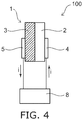
- FIG. 4 is a schematic diagram illustrating an example of a configuration of a photon counting radiation detector according to one or more embodiments.
- 8 denotes a control unit.
- a front surface electrode and a rear surface electrode of each cell is connected to the control unit 8.
- a voltage is applied between the front surface electrode and the rear surface electrode of each cell by the control unit 8.
- the X-rays passing through the inspection subject are incident on the epitaxial layer 2 of the cell structure 1. Incident X-ray photons are absorbed by the epitaxial layer 2. When X-ray photons are absorbed, carriers (electrons and holes) are generated in the epitaxial layer 2. The electrons and holes move toward the front surface electrode and the rear surface electrode, respectively.
- the X-ray photons are directly converted into an electrical signal.
- the control unit 8 detects the magnitude of the current i.
- the magnitude of the current i is proportional to the number of X-ray photons passing through the inspection subject. In other words, by detecting the magnitude of the current i, the number of X-ray photons can be counted. Note that the direction of the voltage applied between the front surface electrode and the rear surface electrode and the current i can be changed as appropriate.
- the photon counting radiation detector preferably includes an array structure in which cell structures are arranged side by side in the lateral direction interposed by insulating spacers.
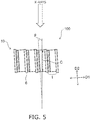
- FIG. 5 illustrates an example of an array structure.
- the array structure 10 has a structure in which a plurality of the cell structures 1 and a plurality of spacers 6 are alternately arranged side by side.
- the spacers 6 preferably have insulating properties.
- the cell structure 1 is provided with the front electrode 4 and the rear electrode 5.
- the front electrode 4 and the rear electrode 5 of each of the cell structures 1 are connected to the control unit 8. Providing insulating spacers allows for conduction between adjacent cell structures to be prevented.
- the spacer 6 may be an insulating resin (including pressure-sensitive adhesives), an insulating film, or the like. Also, an adhesive layer with an insulating film on both sides, such as double-sided tape, may be used.
- the thickness of the spacer 6 is preferably 200 ⁇ m or less, and more preferably 100 ⁇ m or less. By making the thickness of the spacer 6 thin, the regions incapable of detection can be reduced and the spatial resolution can be increased. Note that the number of cell structures arranged side by side is a discretionary number.
- the thickness t sub of a single substrate corresponds to the sum of the thickness of a single substrate 3, the thickness of a single front electrode 4, the thickness of a single rear electrode 5, and the thickness of a single spacer 6.
- the photon counting radiation detector may have a structure in which the array structures 10 are stacked in the X-ray incident direction.
- the array structures 10 By stacking the array structures 10, which include the cell structures 1 arranged side by side in the lateral direction, in the X-ray incident direction, the amount of information able to be measured at one time can be increased.
- X-rays are passed through the epitaxial layer 2. Note that the size of the epitaxial layers 2 of the cell structures 1 forming the array structures 10 stacked vertically may be the same or may be different. In a similar manner, the inclination ⁇ of the substrates may be the same or may be different.
- an X-ray transmission distance C can be different between the upper and lower cells.
- the upper and lower epitaxial layers may overlap or may not overlap. Note that the upper and lower epitaxial layers overlapping is indicative of a structure in which X-rays passing through the upper epitaxial layer 2 are capable of being detected at the lower epitaxial layer 2.
- the inclinations ⁇ of the substrates are preferably within the range of Formula (1).
- FIG. 7 illustrates another example of the array structure 10.
- the X-rays are radially emitted from a light source toward a test subject.
- the X-rays passing through the test subject are incident on the cell structures 1 of the array structure 10.
- the X-ray incident angle is different for each cell structure.
- the array structure 10 includes a cell structure 1-1, a cell structure 1-3, and a cell structure 1-2 located therebetween in the lateral direction.
- An incident direction D X1 of X-rays for the cell structure 1-1, an incident direction D X2 of X-rays for the cell structure 1-2, and an incident direction D X3 of X-rays for the cell structure 1-3 are different from one another.
- inclinations ⁇ 1 to ⁇ 3 of the substrates of the cell structures 1-1 to 1-3 are set on the basis of the incident directions D X1 to D X3 of the X-rays.
- the inclinations ⁇ 1 to ⁇ 3 of the substrates of the cell structures 1-1 to 1-3 are set, with respect to the incident directions D X1 to D X3 of the X-rays, to satisfy Formula (1).
- the plurality of cell structures 1 may be arranged side by side in a straight line as illustrated in FIG. 5 or may be arranged side by side along a curve in the lateral direction as illustrated in FIG. 7 .
- the plurality of cell structures 1 being arranged side by side in the lateral direction includes in its meaning the example illustrated in FIG. 5 of the plurality of cell structures 1 being arranged side by side in a straight line in the lateral direction and the example of the plurality of cell structures 1 being arranged side by side along a curve in the lateral direction.
- FIG. 8 illustrates another example of the array structure 10.
- the cell structures 1 may be arranged in two directions that intersect one another and are perpendicular to the incident direction Dx of the X-rays.
- the cell structures 1 are arranged in a first arrangement direction AD1 and a second arrangement direction AD2 orthogonal to one another and perpendicular to the incident direction Dx.
- the plurality of cell structures 1 arranged side by side in the first arrangement direction AD1 are arranged as illustrated in FIG. 5 or FIG. 7 , for example.
- the inclinations of the substrates of the cell structures 1 arranged in two directions preferably satisfy Formula (1).
- the plurality of cell structures 1 arranged in two directions as illustrated in FIG. 8 may be stacked in the X-ray incident direction Dx as illustrated in FIG. 6 .
- FIG. 9 is a conceptual diagram of a radiation detector.
- 8 denotes a computer functioning as the control unit
- 10 denotes the array structure
- 21 denotes a test subject
- 22 denotes an X-ray tube
- 24 denotes a display
- 25 denotes an image
- 20 denotes an X-ray CT device (radiographic inspection device)
- 100 denotes the photon counting radiation detector.
- An X-ray CT device which is a type of radiographic inspection device, will now be described using FIG. 9 .
- the X-ray CT device 20 is provided with the photon counting radiation detector 100 including the array structure 10.
- the cell structures 1 are arranged side by side along a curve in the lateral direction.
- the array structure 10 is attached to the inner wall of a cylindrical body in which the portion of the test subject 21 to be imaged is placed.
- the X-ray tube 22 that emits X-rays is disposed roughly in the center of the arc along which the array structure 10 is attached.
- the test subject 21 is fixed and placed between the array structure 10 and the X-ray tube 22.
- the array structure 10 and the X-ray tube 22 are configured to rotate about the test subject 21 in a rotation direction 23 while X-ray imaging is performed.
- images are collected from different angles in a three-dimensional space.
- the signals obtained from the X-ray imaging (electrical signals obtained via conversion by the cell structure 1) are processed by the computer 8 and displayed as the image 25 on the display 24.
- the image 25 is a tomogram of the test subject 21, for example.
- the X-ray incident surface can be made smaller, allowing for higher resolution. This can dramatically increase the medical diagnostic capability of the X-ray CT device 20.
- the radiographic inspection device is not limited to being applied to inspection devices for medical diagnosis and may also be applied to industrial X-ray non-destructive inspection devices.
- the radiographic inspection device may also be used in detectors for radiation other than X-rays (for example, gamma rays).
- the photon counting radiation detector 100 according to one or more embodiments is only required to have the configuration described above and is not limited in terms of the manufacturing method. However, an example of a method that can produce a good yield is given below.
- a substrate for forming an epitaxial layer is prepared.
- the substrate includes one type selected from SiC, Ga 2 O 3 , gallium arsenide (GaAs), gallium nitride (GaN), diamond, cadmium telluride (CdTe), IGZO, and a material having a perovskite crystal structure.
- IGZO is a compound of indium (In), gallium (Ga), zinc (Zn), and oxygen (O).
- the thickness t sub of the substrate preferably ranges from 10 ⁇ m to 700 ⁇ m, and more preferably ranges from 15 ⁇ m to 400 ⁇ m.
- the substrate is preferably a single crystal substrate.
- the thickness of the single crystal substrate preferably ranges from 5 ⁇ m to 200 ⁇ m.
- the size of the substrate in terms of length and width is discretionary.
- a substrate larger than the substrate 3 constituting a cell structure is preferably used.
- Forming cell structures by cutting smaller substrates from larger substrates with epitaxial growth improves mass productivity. Also, this cutting process may be performed before providing the electrodes or after providing the electrodes.
- the purity of the substrate is preferably 99.0 wt% or greater.
- the purity of the substrate is preferably 99.0 wt% or greater, and more preferably 99.9 wt% or greater.
- the surface of the substrate is preferably a flat surface with a surface roughness Ra of 0.2 ⁇ m or less.
- Epitaxial growth is a method of growing a crystal on a crystal substrate.
- a crystal can be grown in the same orientation as the crystal surface of the substrate (substrate used as a base).
- the substrate is a single crystal, a single crystal epitaxial layer can also be obtained.
- the growth is called homoepitaxial growth.
- the growth is called heteroepitaxial growth.
- methods of epitaxial growth include vapor-phase epitaxy, liquid-phase epitaxy, solid-phase epitaxy, molecular-beam epitaxy, and the like.
- Vapor-phase epitaxy is a method of depositing a component in the gas-phase on a substrate crystal surface. Vapor-phase epitaxy is also referred to as VPE or chemical vapor deposition (CVD). An example of a type of CVD includes mist CVD.
- liquid-phase epitaxy is also referred to as LPE and is a method in which a crystal component is precipitated from a super saturated solution onto a substrate crystal surface.
- Solid-phase epitaxy is a method in which material deposited on a substrate crystal surface is heated by electron beam irradiation to change the structure of the material to the same crystal structure as the substrate crystal. Solid-phase epitaxy is also referred to as SPE.
- molecular-beam epitaxy is a method in which an element for forming the target crystal or a material including the element is heated and evaporated in an ultra-high vacuum (from 10 -3 to 10 -9 Pa) and a crystal is deposited on a heated substrate crystal.
- Molecular-beam epitaxy is also referred to as MBE.
- Epitaxial growth is continued until the epitaxial layer reaches the target thickness.
- the grown epitaxial layer here corresponds to the epitaxial layer 2.
- the thickness of the epitaxial layer 2 is preferably 100 ⁇ m or less, and more preferably ranges from 1 ⁇ m to 30 ⁇ m.
- the thickness t sub of the substrate is adjusted as necessary.
- a thinner thickness of the substrate t sub allows the spatial resolution to be improved.
- the thickness t sub of the substrate preferably ranges from 5 ⁇ m to 500 ⁇ m, and more preferably ranges from 5 ⁇ m to 100 ⁇ m.
- the thickness t sub of the substrate can be reduced by machining/finishing and etching.
- the electrode material is preferably one type selected from a metal, a metal oxide, a metal carbide, and a metal silicide. Also, sputtering, chemical vapor deposition (CVD), ion plating, vapor deposition, thermal spraying, plating, and the like may be used as the film forming method. These film forming methods allow electrodes to be formed at discretionary locations. Also, the electrode may be formed on the entire front surface of the epitaxial layer 2 or may be formed on a portion of the front surface. Furthermore, a plurality of electrodes may be formed on the front surface of the epitaxial layer 2.
- the electrode provided on the rear surface of the substrate 3 may be formed on the entire rear surface or may be formed on a portion of the rear surface.
- a plurality of electrodes may be formed on the rear surface of the substrate 3.
- the electrode may be patterned via etching. Heat treatment may be performed in addition as necessary. Also, heating may be performed during the film forming of the electrode.
- the epitaxial layer 2 or the substrate 3 includes silicon carbide (SiC) or diamond
- a metal carbide electrode or a metal silicide electrode is preferable.
- Mo 2 C, W, WC, or W 2 C is preferable.
- the epitaxial layer 2 and the substrate 3 include a carbon component
- a metal carbide electrode or a metal silicide electrode can be used to help suppress a reaction between the electrode and the epitaxial layer or between the electrode and the substrate. In this way, stable electrical characteristics can be obtained. Also, the cell structure can have a long service life.
- the epitaxial layer 2 or the substrate 3 includes gadolinium oxide (Ga 2 O 3 ), gallium arsenide (GaAs), gallium nitride (GaN), or cadmium telluride (CdTe), a metal electrode or a metal oxide electrode is preferable.
- Gadolinium oxide Ga 2 O 3
- GaAs gallium arsenide
- GaN gallium nitride
- CdTe cadmium telluride
- a metal electrode or a metal oxide electrode is preferable.
- Pt, Ni, or TiO 2 is preferable.
- the electrode may include titanium nitride (TiN). This can help suppress a reaction between the electrode and the epitaxial layer or between the electrode and the substrate.
- the cell structures are completed via the process described above.
- an array structure is manufactured by arranging the cell structures side by side.
- wiring is connected to the electrodes of each cell structure.
- the cell structures are arranged side by side interposed by the spacers.
- the cell structures are arranged with the inclination ⁇ of the substrate satisfying Formula (1) with respect to the X-ray incident direction.
- the spacers preferably have insulating properties.
- the cell structures 1 are each provided with the front electrode 4 and the rear electrode 5. Providing insulating spacers allows for conduction between adjacent cell structures to be prevented.
- the spacer 6 may be an insulating resin (including pressure-sensitive adhesives) or an insulating film.
- an adhesive layer with insulating film on both sides such as double-sided tape, may be used.
- the thickness of the spacer is preferably 200 ⁇ m or less, and more preferably 100 ⁇ m or less. By making the thickness of the spacer thin, the regions incapable of detection can be reduced and the spatial resolution can be increased. Note that the number of cell structures arranged side by side is a discretionary number.
- the array structure may be resin-molded as necessary. Resin molding allows the strength of the array structure to be increased.
- SiC substrates according to Examples 1 to 3 were prepared. Epitaxial growth was performed on the SiC layer on the SiC substrate. For Examples 4 to 6, Ga 2 O 3 substrates were prepared. Epitaxial growth was performed on the Ga 2 O 3 layer on the Ga 2 O 3 substrate. For Examples 7 to 9, GaN substrates were prepared. Epitaxial growth was performed on the GaN layer on the GaN substrate. A single crystal was used for the SiC substrates, the Ga 2 O 3 substrates, and the GaN substrates. Thus, single crystal epitaxial layers were obtained.
- the sizes of the substrates and the epitaxial layers are as listed in Table 1. Furthermore, the thickness t sub of the substrate is a thickness that includes the thickness of the electrodes and the insulating layer.
- the thickness t sub of the substrate is a thickness that includes the thickness of the electrodes and the insulating layer.
- Epitaxial layer Substrate (including insulating layer) Material Thickness t epi ( ⁇ m) Impurity concentration (cm -3 ) Material Thickness t sub ( ⁇ m) Impurity concentration (cm -3 )
- Electrodes were provided.
- the material of the electrode layers is as listed in Table 2. Note that the front electrode and the rear electrode have the same material, and the film thickness is 20 ⁇ m in all Examples. In this way, cell structures according to the Examples were manufactured. Also, an insulating layer ranging from 10 ⁇ m to 150 ⁇ m was used, this value being included in the thickness t sub of the substrate listed in Table 1.
- Example 1 Sample Electrode material Example 1-1 Example 1 WC Example 2-1 Example 2 TiC Example 2-2 Example 2 Mo 2 C Example 2-3 Example 2 W Example 2-4 Example 2 WC Example 2-5 Example 2 W 2 C Example 3-1 Example 3 WC Example 4-1 Example 4 TiN Example 5-1 Example 5 TiN Example 6-1 Example 6 Ni Example 7-1 Example 7 Pt Example 8-1 Example 8 Ni Example 9-1 Example 9 Ni
- the I-V characteristics of the cell structures of Examples 2-1 to 2-5 were examined.
- the I-V characteristics were examined after heat treating the cell structures at temperatures of 500°C, 700°C, 800°C, 900°C, and 1000°C in a nitrogen atmosphere for 1 minute.
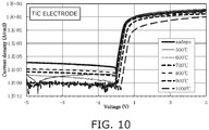
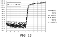
- the I-V characteristics of Examples 2-1 to 2-5 are shown in FIGS. 10 to 14 .
- the horizontal axis indicates voltage (v), and the vertical axis indicates current density (A/cm 2 ).
- asdepo indicates the characteristics of the unheat treated cell structure.
- the I-V characteristics shown in FIGS. 10 to 14 were used to examine for increases in the reverse leakage current at each temperature of the heat treatment. Large differences in the I-V characteristics graph at the different heat treatment temperatures indicate an increase in the reverse leakage current. Also, a large current density when the voltage is in the negative region indicates a large reverse leakage current.
- the TiC electrode ( FIG. 10 ) has a strong tendency toward an increase in the reverse leakage current.
- the Mo 2 C electrode ( FIG. 11 ), the W electrode ( FIG. 12 ), the WC electrode ( FIG. 13 ), and the W 2 C electrode ( FIG. 14 ) have little reverse leakage current.
- the electrode material is preferably one type selected from Mo 2 C, W, WC, and W 2 C.
- cell structures using a Ga 2 O 3 epitaxial layer or a GaN epitaxial layer also followed this pattern.
- the cell structures were manufactured with the substrate lengths L listed in Table 3.
- Array structures were manufactured by arranged the cell structures side by side.
- the length L of each cell are the values listed in Table 3.
- the sizes in terms of length and width are the same.
- the inclination ⁇ of each substrate of the array structures are the values listed in Table 3.
- Example 1-1 1mm ⁇ 10 368 No Comparative Example A
- Example C Example 2-1 1cm ⁇ 1 205 No Example D
- Example 2-2 1mm ⁇ 1 205 No Example E
- Example 2-3 1mm ⁇ 3 205 No Example F
- Example 2-4 1mm ⁇ 5 205 No Example G
- Example 2-5 1mm ⁇ 10 208 No Comparative Example B
- Example 3-1 1mm ⁇ 6 160 No Comparative Example C
- Example J Example 4-1 1cm ⁇ 0.3 52 No Example K
- Example 4-1 1mm ⁇ 2 52 No Example M
- Example 5-1 1cm ⁇ 1 104 No Example N
- Radiation detectors according to the embodiments described above exhibit excellent performance.
- the Examples due to Mathematical Formula 1 being satisfied, no detection contamination in adjacent cell structures was found. Also, it can be seen that even in configurations with the same substrate length L, for example, Example B and Comparative Example A, when the inclination ⁇ of the substrate satisfies Mathematical Formula 1, the detection pixel can be made smaller. Thus, higher resolution can be achieve.
- photon counting radiation detectors according to the Examples display good sensitivity due to the detection layer being an epitaxial layer. Furthermore, even when the pixel size is reduced to 1 mm (1000 ⁇ m) or less, X-ray photons can be detected.
- Photon counting radiation detectors are also capable of detecting a current of a few ⁇ A (microamperes) based on an X-ray photon. Furthermore, it was confirmed that increasing the inclination ⁇ of the substrate increases the detection current. This is because the distance of the X-rays passing through the epitaxial layer is increased.
Landscapes
- Physics & Mathematics (AREA)
- Health & Medical Sciences (AREA)
- Life Sciences & Earth Sciences (AREA)
- General Physics & Mathematics (AREA)
- High Energy & Nuclear Physics (AREA)
- Molecular Biology (AREA)
- Spectroscopy & Molecular Physics (AREA)
- Measurement Of Radiation (AREA)
- Light Receiving Elements (AREA)
Abstract
Description
- One or more embodiments generally relate to a photon counting radiation detector and a radiographic inspection device using the same.
- Radiographic inspection devices are used in various fields as medical devices, industrial non-destructive inspection devices, and the like. Examples of such medical devices include computed tomography (CT) devices and positron emission tomography (PET) devices. Also, the radiation used may be X-rays, gamma rays, or the like.
- As described in
JP 4886151B - In recent years, the development of a radiation detector in which the radiation passing through a test subject is converted directly into an electrical signal has been progressing. In
JP S63-40381A -
- [Patent Document 1]
JP 4886151B - [Patent Document 2]
JP S63-40381A - In
Patent Document 2, a structure including semiconductor elements disposed inclined with respect to an incident direction of radiation is described. In this structure, at least two of the semiconductor elements are disposed overlapping one another. This alleviates the radiation incident position dependency of the total charge induced at the electrode surface. - However, there is a demand for high resolution in radiographic inspection devices such a CT device. Small detection pixels are needed for high resolution. With higher resolution, more detailed images can be obtained. In
Patent Document 2, the aperture ratio of the detection elements is not reduced. Thus, there is a limit to how much resolution can be increased. - This invention was made in light of the problem described above and provides a photon counting radiation detector capable of obtaining higher resolution images.
- A photon counting radiation detector according to one or more embodiments includes: a cell structure including a substrate, and an epitaxial layer provided on the substrate, radiation being incident on the epitaxial layer; an inclination θ of the substrate satisfying Formula (1) below, where tsub is a thickness of the substrate, tepi is a thickness of the epitaxial layer, L is a length of the substrate, and the inclination θ is an inclination of the substrate with respect to an incident direction of the radiation;

- A photon counting radiation detector according to one or more embodiments includes an epitaxial layer, allowing the incident surface of radiation to be made small. Also, an inclination θ of the substrate is set within a specific range, allowing for higher resolution of images.
-
- [
FIG. 1] FIG. 1 is a schematic diagram illustrating an example of a photon counting radiation detector according to an embodiment. - [
FIG. 2] FIG. 2 is a schematic diagram illustrating an example of an array structure according to an embodiment. - [
FIG. 3] FIG. 3 is a schematic diagram illustrating another example of a photon counting radiation detector according to an embodiment. - [
FIG. 4] FIG. 4 is a schematic diagram illustrating another example of a photon counting radiation detector according to an embodiment. - [
FIG. 5] FIG. 5 is a schematic diagram illustrating another example of an array structure according to an embodiment. - [
FIG. 6] FIG. 6 is a schematic diagram illustrating another example of an array structure according to an embodiment. - [
FIG. 7] FIG. 7 is a schematic diagram illustrating another example of an array structure according to an embodiment. - [
FIG. 8] FIG. 8 is a schematic diagram illustrating another example of an array structure according to an embodiment. - [
FIG. 9] FIG. 9 is a diagram illustrating an example of a radiographic inspection device according to an embodiment. - [
FIG. 10] FIG. 10 is a diagram illustrating the I-V characteristics of a cell structure according to Example 2-1. - [
FIG. 11] FIG. 11 is a diagram illustrating the I-V characteristics of a cell structure according to Example 2-2. - [
FIG. 12] FIG. 12 is a diagram illustrating the I-V characteristics of a cell structure according to Example 2-3. - [
FIG. 13] FIG. 13 is a diagram illustrating the I-V characteristics of a cell structure according to Example 2-4. - [
FIG. 14] FIG. 14 is a diagram illustrating the I-V characteristics of a cell structure according to Example 2-5. - A photon counting radiation detector according to one or more embodiments includes: a cell structure including a substrate, and an epitaxial layer provided on the substrate, radiation being incident on the epitaxial layer; an inclination θ of the substrate satisfying Formula (1) below, where tsub is a thickness of the substrate, tepi is a thickness of the epitaxial layer, L is a length of the substrate, and the inclination θ is an inclination of the substrate with respect to an incident direction of the radiation.

-
FIG. 1 illustrates an example of the cell structure. InFIG. 1, 1 denotes the cell structure, 2 denotes the epitaxial layer, 3 denotes the substrate, 100 denotes the photon counting radiation detector, tsub denotes the thickness of the substrate, tepi denotes the thickness of theepitaxial layer 2, L denotes the length of the substrate, and θ denotes the inclination of the substrate with respect to an X-ray incident direction. The photon countingradiation detector 100 includes thecell structure 1. The photon counting radiation detector is formed by disposed wiring, an insulating layer, and the like (not illustrated) in the cell structure. Herein, the cell structure will mainly be described. Also, the photon countingradiation detector 100 is capable of detecting radiation, such as X-rays and gamma rays. In the example described herein, the photon countingradiation detector 100 detects X-rays. The technology described below can also be applied in a similar manner to a photon countingradiation detector 100 that detects gamma rays. -
FIG. 2 illustrates an example of an array structure including cell structures arranged side by side. InFIG. 2, 2 denotes the epitaxial layer, 3 denotes the substrate, tsub denotes the thickness of the substrate, tepi denotes the thickness of theepitaxial layer 2, θ denotes the inclination of the substrate with respect to an X-ray incident direction, 6 denotes a spacer, and 10 denotes the array structure. Note that the thickness tsub of the substrate is a value that includes the thickness of the substrate, the electrode, and the insulating layer. - The thickness tsub of the substrate is, in other words, the length of the
substrate 3 in a first direction D1 connecting theepitaxial layer 2 and thesubstrate 3. The thickness tepi of the epitaxial layer is the length of theepitaxial layer 2 in the first direction D1. The length L of the substrate is the length of thesubstrate 3 in a second direction D2 perpendicular to the first direction D1. The second direction D2 is parallel with a plane that runs in both the first direction D1 and an X-ray incident direction Dx. The inclination θ corresponds to the angle between the X-ray incident direction and the second direction D2. - The relationship between the thickness tsub of the substrate, the thickness tepi of the epitaxial layer, the length L of the substrate, and the inclination θ of the substrate satisfies the following Formula (2).

- The cell structure includes the
substrate 3 and theepitaxial layer 2 provided on thesubstrate 3. The substrate of the cell structure is inclined with respect to the X-ray incident direction. Note that for the inclination θ of the substrate, the X-ray incident direction is 0°. Also, when the substrate is inclined to the down and right, θ is a positive angle. When the substrate is inclined to the down and left, θ is a negative angle. In the state illustrated inFIG. 2 , θ is a positive angle. Also, in Formula (2), the inclination θ of thesubstrate 3 is an absolute value. In other words, in Formula (2), the inclination θ is given as a positive angle even when it is a negative angle. The incident direction is perpendicular to the direction in which the plurality ofcell structures 1 are arranged side by side, for example. - The
substrate 3 is used to form theepitaxial layer 2. Also, theepitaxial layer 2 is capable of converting incident X-ray photons into electrical signals. By the epitaxial layer being present continuously with respect to the X-ray incident direction, the regions incapable of detecting X-ray photons can be reduced. However, the plurality of cell structures need to be disposed without overlapping theepitaxial layers 2 of adjacent cell structures with respect to the X-ray incident direction. If adjacentepitaxial layers 2 are overlapped, contamination occurs when X-ray photons are detected. As a result, X-ray photons are unable to be accurately detected. Contamination is image blur caused by a plurality of theepitaxial layers 2 detecting the same X-ray photon. InPatent Document 2, contamination of X-ray photon detection is prevented by covering the semiconductor element with a shielding material. Lead is used in the shielding material. However, lead is a toxic material that is hard to use. - In the cell structure according to one or more embodiments, the inclination θ of the substrate with respect to the X-ray incident direction is set within a specific range. By setting the inclination of the substrate depending on the thickness of the substrate, the length of the substrate, and the thickness of the epitaxial layer, the regions incapable of detection can be reduced and detection contamination can be suppressed.
- Formula (2) will now be described.
- First, as illustrated in
FIG. 2 , [(tsub + tepi)/cosθ - (tsub + tepi)cosθ] must take a value equal to or greater than 0. (tsub + tepi)/cosθ is the width of asingle epitaxial layer 2 as seen from the X-ray incident direction. (tsub + tepi)/cosθ is the pixel size. (tsub + tepi)cosθ is the width from the lower end portion of thesubstrate 3 to the lower end portion of theepitaxial layer 2 as seen from the X-ray incident direction. The width is, in other words, the length in the direction perpendicular to the X-ray incident direction and in the direction in which thecell structures 1 are arranged. - As [(tsub + tepi)/cosθ - (tsub + tepi)cosθ] approaches zero, the angle between the inclination θ of the
substrate 3 and the X-ray incident direction decreases. - Also, the relationship of Formula (3) is applied so that adjacent cell structures are disposed with the
epitaxial layers 2 not overlapped with respect to the X-ray incident direction.

- Formula (3) is represented by Formula (4).

- From Formula (4), the relationship of Formula (1) is satisfied for the inclination θ of the substrate.

- Also, the following Formula (4) is satisfied.

- Formula (1) being satisfied for the inclination θ of the
substrate 3 means that adjacent cell structures are disposed with theepitaxial layers 2 not overlapped with respect to the X-ray incident direction. - If the
epitaxial layers 2 of adjacent cell structures are overlapped with respect the X-ray incident direction, image blur occurs. This is because a single X-ray photon is detected by two cells. - Also, the inclination θ of the substrate is an absolute value of the angle of the substrate with respect to the X-ray incident direction. Thus, the angle of the substrate with respect to the X-ray incident direction may be a positive angle or a negative angle. Also, the inclination θ of the substrate is preferably a value greater than 0°. When the inclination θ of the substrate is 0°, the substrate is parallel with the X-ray incident direction. When the inclination θ of the substrate is 0°, contamination (image blur) of the detection by adjacent cell structures does not occur. However, the region of the thickness tsub of the
substrate 3 is made a region incapable of detecting X-ray photons. In other words, when a gap is formed between theepitaxial layers 2 of adjacent cell structures with respect to the X-ray incident direction, a region incapable of detection is formed. - Also, increasing the inclination θ of the substrate makes (tsub + tepi)/cosθ decrease. This allows the pixels to be made smaller.
- In other words, by adjusting the inclination θ of the substrate while satisfying Formula (1), image blur can be prevented and the pixels can be made smaller.
- Thus, the inclination θ of the
substrate 3 is preferably a value greater than 0°, while satisfying Formula (1). By setting the inclination θ of thesubstrate 3 within this range, detection contamination suppression and higher resolution can both be achieved in a compatible manner. - The cell structure includes the
epitaxial layer 2 provided on thesubstrate 3. Theepitaxial layer 2 preferably includes one type selected from SiC, Ga2O3, GaAs, GaN, diamond, and CdTe. Also, thesubstrate 3 preferably includes one type selected from SiC, Ga2O3, GaAs, GaN, diamond, and CdTe. Furthermore, theepitaxial layer 2 is preferably a layer grown epitaxially on thesubstrate 3. Because of this, the materials of theepitaxial layer 2 and thesubstrate 3 are preferably the same. Also, theepitaxial layer 2 and thesubstrate 3 are preferably made from SiC or Ga2O3. Epitaxial growth on the substrate is easy when these materials are used. Also, the substrate can be easily thinned using the etching process described below. Furthermore, because X-rays pass through these substrate materials, there are no negative effects on the detection of X-rays via theepitaxial layer 2. Theepitaxial layer 2 and thesubstrate 3 may be made of a single crystal. - Also, when SiC is used in the
epitaxial layer 2, 4H-SiC is preferably used. SiC polytypes include 4H-SiC, 6H-SiC, and 3C-SiC. Of these, 4H-SiC has the largest band gap of 3.25 eV. By using a material with a large band gap, leakage current can be reduced. These materials also allow for operations at room temperature. - The
epitaxial layer 2 is a high-quality layer compared to thesubstrate 3. Specifically, the impurity concentration and the density of defect states of theepitaxial layer 2 per unit volume is less than those of thesubstrate 3 by at least two orders of magnitude. For example, when the impurity concentration of a SiC substrate is approximately 1018 cm-3, the impurity concentration of a SiC epitaxial layer is 1016 cm-3 or less. - The same holds true for the density of defect states. Also, the
epitaxial layer 2 and thesubstrate 3 are discernable by observing the cross-sectional structure. Theepitaxial layer 2 has a higher density than thesubstrate 3. In particular, by using a single-crystal substrate, theepitaxial layer 2 can also be single crystal. When a single-crystal substrate 2 is used, a high-quality epitaxial layer can be easily formed. - Also, the amount of impurities can be calculated from the relationship between the reverse voltage and the depletion layer capacitance. The reverse voltage is set as V, the depletion layer capacitance is set as C, the Schottky barrier is set as ϕB, the load is set as q, the impurity concentration is set as Nd, and the dielectric constant of the material is set as ε. The relationship between the reverse voltage V and the depletion layer capacitance C satisfies the relationship formula: 1/C2 = -2(V - ϕB)/q Ndε.
- The dielectric constant ε of the material is the dielectric constant of the material the
epitaxial layer 2 and thesubstrate 3 are made of. For example, the dielectric constant ε of SiC is 9.7, the dielectric constant ε of GaN is 9.0, the dielectric constant ε of Ga2O3 is 10.0, and the dielectric constant ε of diamond is 5.5. - By measuring the reverse voltage V and the depletion layer capacitance C (1/C2), the impurity concentration Nd can be calculated using the relationship formula described above. The impurity concentration Nd is also referred to as donor concentration.
- Also, for the reverse voltage V, preferably an LCR meter capable of applying a high voltage of approximately -200 V is used. By applying a high voltage, depletion of the
substrate 3 begins after the depletion of theepitaxial layer 2. This allows measurements to be performed with theepitaxial layer 2 and thesubstrate 3 in an integrally formed state. - Also, by setting the inclination θ of the substrate to a predetermined value, the side surface of the
epitaxial layer 2 can be an X-ray incident surface. This allows the incident surface to be made smaller. By making the incident surface smaller, the detection pixels can be made smaller. Also, the thickness tepi of the epitaxial layer is preferably 100 µm or less. The thickness tepi of the epitaxial layer is more preferably 30 µm or less, and even more preferably 10 µm or less. A thin thickness tepi allows the detection pixels to be made smaller. The minimum value of the thickness tepi of theepitaxial layer 2 is not particularly limited, but is preferably 1 µm or greater. A thickness tepi of less than 1 µm produces an electrical signal that is too small. - The thickness tsub of the substrate is preferably 500 µm or less. When the thickness tsub of the substrate is greater than 500 µm, regions incapable of detection may increase. Thus, the thickness tsub of the substrate is preferably 500 µm or less, and more preferably 100 µm or less. Also, the lower limit value of the thickness tsub of the substrate is not particularly limited, but is preferably 5 µm or greater. When the thickness tsub of the substrate is less than 5 µm, the strength of the substrate is reduced. A substrate with low strength may be easily damaged when the array structure is assembled. Thus, the thickness tsub of the substrate preferably ranges from 5 µm to 500 µm, and more preferably ranges from 5 µm to 100 µm. By making the substrate thin, the regions incapable of detection can be reduced and the spatial resolution can be improved. Also, the thickness of the substrate can be adjusted by using a substrate with a predetermined thickness or by thinning the substrate via machining/finishing or etching. Furthermore, the thickness of the electrode, the insulating layer, and the like are included in the thickness tsub of the substrate.
- An electrode is preferably provided in the cell structure. The electrode provided in the cell structure preferably includes one or two or more types selected from the group consisting of carbon, silicon, titanium, platinum, and nickel.
-
FIG. 3 illustrates an example of a cell structure provided with electrodes. InFIG. 3 ,1 denotes the cell structure, 2 denotes the epitaxial layer, 3 denotes the substrate, 4 denotes a front electrode, 5 denotes a rear electrode, and 100 denotes the photon counting radiation detector. InFIG. 3 , the electrode provided on the side theepitaxial layer 2 is provided on corresponds to thefront electrode 4, and the electrode provided on thesubstrate 3 corresponds to therear electrode 5. Also, inFIG. 3 , the cell structure is illustrated as seen from the side surface. - The
front electrode 4 is provided on the entire surface or a portion of theepitaxial layer 2. Also, a plurality of thefront electrodes 4 may be provided on the front surface of theepitaxial layer 2. - The
rear electrode 5 is provided on the entire surface or a portion of the rear surface of thesubstrate 3. Also, a plurality of therear electrodes 5 may be provided on the rear surface of thesubstrate 3. - The thickness tsub of the substrate corresponds to the sum of the thickness of the
substrate 3, the thickness of thefront electrode 4, and the thickness of therear electrode 5. - Also, the electrode material is preferably one type selected from a metal, a metal oxide, a metal carbide, and a metal silicide.
- For a metal electrode, one type selected from titanium (Ti), tungsten (W), molybdenum (Mo), tantalum (Ta), niobium (Nb), platinum (Pt), and nickel (Ni) is preferably used. For a metal oxide electrode, titanium oxide (TiO2) is preferably used. For a metal carbide electrode, one type selected from titanium carbide (TiC), tungsten carbide (WC), molybdenum carbide (Mo2C), tantalum carbide (TaC), and niobium carbide (NbC) is preferably used. For a metal silicide electrode, one type selected from titanium silicide (TiSi2), tungsten silicide (WSi2), molybdenum silicide (MoSi2), tantalum silicide (TaSi2), and niobium silicide (NbSi2) is preferably used.
- When the
epitaxial layer 2 and thesubstrate 3 include silicon carbide (SiC) or diamond, a metal carbide electrode or a metal silicide electrode is preferably provided. Among these, Mo2C, W, WC, and W2C are preferable. When theepitaxial layer 2 and thesubstrate 3 include a carbon component, a metal carbide electrode or a metal silicide electrode can be used to help suppress a reaction between the electrode and the epitaxial layer (or the substrate). In this way, stable electrical characteristics can be obtained. Also, the cell structure can have a long service life. - Also, when the
epitaxial layer 2 and thesubstrate 3 include gadolinium oxide (Ga2O3), gallium arsenide (GaAs), gallium nitride (GaN), or cadmium telluride (CdTe), a metal electrode or a metal oxide electrode is preferably used. Among these, Pt, Ni, and TiO2 are preferable. Also, titanium nitride (TiN) may be used in the electrode. This can help suppress a reaction between the electrode and the epitaxial layer (or the substrate). - The metal electrode, the metal carbide electrode, and the metal silicide electrode can be formed via sputtering. Methods that may be used other than sputtering include chemical vapor deposition (CVD), ion plating, vapor deposition, thermal spraying, plating, and the like.
-
FIG. 4 is a schematic diagram illustrating an example of a configuration of a photon counting radiation detector according to one or more embodiments. InFIG. 4 ,8 denotes a control unit. A front surface electrode and a rear surface electrode of each cell is connected to thecontrol unit 8. A voltage is applied between the front surface electrode and the rear surface electrode of each cell by thecontrol unit 8. The X-rays passing through the inspection subject are incident on theepitaxial layer 2 of thecell structure 1. Incident X-ray photons are absorbed by theepitaxial layer 2. When X-ray photons are absorbed, carriers (electrons and holes) are generated in theepitaxial layer 2. The electrons and holes move toward the front surface electrode and the rear surface electrode, respectively. This makes a current i flow between the control unit and the front surface electrode, and the control unit and the rear surface electrode, as illustrated inFIG. 4 . In other words, in theepitaxial layer 2, the X-ray photons are directly converted into an electrical signal. Thecontrol unit 8 detects the magnitude of the current i. The magnitude of the current i is proportional to the number of X-ray photons passing through the inspection subject. In other words, by detecting the magnitude of the current i, the number of X-ray photons can be counted. Note that the direction of the voltage applied between the front surface electrode and the rear surface electrode and the current i can be changed as appropriate. - The photon counting radiation detector preferably includes an array structure in which cell structures are arranged side by side in the lateral direction interposed by insulating spacers.
FIG. 5 illustrates an example of an array structure. Thearray structure 10 has a structure in which a plurality of thecell structures 1 and a plurality ofspacers 6 are alternately arranged side by side. Thespacers 6 preferably have insulating properties. As illustrated inFIG. 3 , thecell structure 1 is provided with thefront electrode 4 and therear electrode 5. As illustrated inFIG. 4 , thefront electrode 4 and therear electrode 5 of each of thecell structures 1 are connected to thecontrol unit 8. Providing insulating spacers allows for conduction between adjacent cell structures to be prevented. For example, thespacer 6 may be an insulating resin (including pressure-sensitive adhesives), an insulating film, or the like. Also, an adhesive layer with an insulating film on both sides, such as double-sided tape, may be used. The thickness of thespacer 6 is preferably 200 µm or less, and more preferably 100 µm or less. By making the thickness of thespacer 6 thin, the regions incapable of detection can be reduced and the spatial resolution can be increased. Note that the number of cell structures arranged side by side is a discretionary number. - When the
spacers 6 are provided, the thickness tsub of a single substrate corresponds to the sum of the thickness of asingle substrate 3, the thickness of a singlefront electrode 4, the thickness of a singlerear electrode 5, and the thickness of asingle spacer 6. - As illustrated in
FIG. 6 , the photon counting radiation detector may have a structure in which thearray structures 10 are stacked in the X-ray incident direction. By stacking thearray structures 10, which include thecell structures 1 arranged side by side in the lateral direction, in the X-ray incident direction, the amount of information able to be measured at one time can be increased. Also, for a structure including stackedarray structures 10, preferably X-rays are passed through theepitaxial layer 2. Note that the size of theepitaxial layers 2 of thecell structures 1 forming thearray structures 10 stacked vertically may be the same or may be different. In a similar manner, the inclination θ of the substrates may be the same or may be different. By having different sizedepitaxial layers 2 or different inclinations θ, an X-ray transmission distance C can be different between the upper and lower cells. Also, when thearray structures 10 are stacked, the upper and lower epitaxial layers may overlap or may not overlap. Note that the upper and lower epitaxial layers overlapping is indicative of a structure in which X-rays passing through theupper epitaxial layer 2 are capable of being detected at thelower epitaxial layer 2. Also, even with a structure in which thearray structures 10 are stacked in the X-ray incident direction, the inclinations θ of the substrates are preferably within the range of Formula (1). -
FIG. 7 illustrates another example of thearray structure 10. In this example, the X-rays are radially emitted from a light source toward a test subject. The X-rays passing through the test subject are incident on thecell structures 1 of thearray structure 10. With radially emitted X-rays, the X-ray incident angle is different for each cell structure. For example, thearray structure 10 includes a cell structure 1-1, a cell structure 1-3, and a cell structure 1-2 located therebetween in the lateral direction. An incident direction DX1 of X-rays for the cell structure 1-1, an incident direction DX2 of X-rays for the cell structure 1-2, and an incident direction DX3 of X-rays for the cell structure 1-3 are different from one another. In this case, inclinations θ1 to θ3 of the substrates of the cell structures 1-1 to 1-3 are set on the basis of the incident directions DX1 to DX3 of the X-rays. The inclinations θ1 to θ3 of the substrates of the cell structures 1-1 to 1-3 are set, with respect to the incident directions DX1 to DX3 of the X-rays, to satisfy Formula (1). - The plurality of
cell structures 1 may be arranged side by side in a straight line as illustrated inFIG. 5 or may be arranged side by side along a curve in the lateral direction as illustrated inFIG. 7 . Herein, the plurality ofcell structures 1 being arranged side by side in the lateral direction includes in its meaning the example illustrated inFIG. 5 of the plurality ofcell structures 1 being arranged side by side in a straight line in the lateral direction and the example of the plurality ofcell structures 1 being arranged side by side along a curve in the lateral direction. -
FIG. 8 illustrates another example of thearray structure 10. As illustrated inFIG. 8 , thecell structures 1 may be arranged in two directions that intersect one another and are perpendicular to the incident direction Dx of the X-rays. For example, thecell structures 1 are arranged in a first arrangement direction AD1 and a second arrangement direction AD2 orthogonal to one another and perpendicular to the incident direction Dx. The plurality ofcell structures 1 arranged side by side in the first arrangement direction AD1 are arranged as illustrated inFIG. 5 orFIG. 7 , for example. The inclinations of the substrates of thecell structures 1 arranged in two directions preferably satisfy Formula (1). Also, the plurality ofcell structures 1 arranged in two directions as illustrated inFIG. 8 may be stacked in the X-ray incident direction Dx as illustrated inFIG. 6 . - Also, the photon counting radiation detector according to one or more embodiments may be used in a radiation detector.
FIG. 9 is a conceptual diagram of a radiation detector. In the diagram, 8 denotes a computer functioning as the control unit, 10 denotes the array structure, 21 denotes a test subject, 22 denotes an X-ray tube, 24 denotes a display, 25 denotes an image, 20 denotes an X-ray CT device (radiographic inspection device), and 100 denotes the photon counting radiation detector. An X-ray CT device, which is a type of radiographic inspection device, will now be described usingFIG. 9 . - The
X-ray CT device 20 is provided with the photon countingradiation detector 100 including thearray structure 10. In thearray structure 10, thecell structures 1 are arranged side by side along a curve in the lateral direction. Thearray structure 10 is attached to the inner wall of a cylindrical body in which the portion of the test subject 21 to be imaged is placed. TheX-ray tube 22 that emits X-rays is disposed roughly in the center of the arc along which thearray structure 10 is attached. Thetest subject 21 is fixed and placed between thearray structure 10 and theX-ray tube 22. - The
array structure 10 and theX-ray tube 22 are configured to rotate about the test subject 21 in arotation direction 23 while X-ray imaging is performed. In the image processing of thetest subject 21, images are collected from different angles in a three-dimensional space. The signals obtained from the X-ray imaging (electrical signals obtained via conversion by the cell structure 1) are processed by thecomputer 8 and displayed as theimage 25 on thedisplay 24. Theimage 25 is a tomogram of thetest subject 21, for example. - In the photon counting
radiation detector 100 of one or more embodiments, the X-ray incident surface can be made smaller, allowing for higher resolution. This can dramatically increase the medical diagnostic capability of theX-ray CT device 20. - Also, the radiographic inspection device according to one or more embodiments is not limited to being applied to inspection devices for medical diagnosis and may also be applied to industrial X-ray non-destructive inspection devices. The radiographic inspection device according to one or more embodiments may also be used in detectors for radiation other than X-rays (for example, gamma rays).
- Next, a method for manufacturing the photon counting
radiation detector 100 according to one or more embodiments will be described. The photon countingradiation detector 100 according to one or more embodiments is only required to have the configuration described above and is not limited in terms of the manufacturing method. However, an example of a method that can produce a good yield is given below. - First, a substrate for forming an epitaxial layer is prepared. The substrate includes one type selected from SiC, Ga2O3, gallium arsenide (GaAs), gallium nitride (GaN), diamond, cadmium telluride (CdTe), IGZO, and a material having a perovskite crystal structure. Note that IGZO is a compound of indium (In), gallium (Ga), zinc (Zn), and oxygen (O).
- The thickness tsub of the substrate preferably ranges from 10 µm to 700 µm, and more preferably ranges from 15 µm to 400 µm. Also, the substrate is preferably a single crystal substrate. The thickness of the single crystal substrate preferably ranges from 5 µm to 200 µm.
- The size of the substrate in terms of length and width is discretionary. A substrate larger than the
substrate 3 constituting a cell structure is preferably used. Forming cell structures by cutting smaller substrates from larger substrates with epitaxial growth improves mass productivity. Also, this cutting process may be performed before providing the electrodes or after providing the electrodes. - Furthermore, the purity of the substrate is preferably 99.0 wt% or greater. When the substrate has low purity, impurities are more likely to contaminate the epitaxial layer. Thus, the purity of the substrate is preferably 99.0 wt% or greater, and more preferably 99.9 wt% or greater. Also, the surface of the substrate is preferably a flat surface with a surface roughness Ra of 0.2 µm or less.
- Next, epitaxial growth on the substrate is performed to form the epitaxial layer. Epitaxial growth is a method of growing a crystal on a crystal substrate. A crystal can be grown in the same orientation as the crystal surface of the substrate (substrate used as a base). When the substrate is a single crystal, a single crystal epitaxial layer can also be obtained.
- Also, when the substrate and the epitaxial layer are the same material, the growth is called homoepitaxial growth. When the substrate and the epitaxial layer are different materials, the growth is called heteroepitaxial growth.
- Furthermore, methods of epitaxial growth include vapor-phase epitaxy, liquid-phase epitaxy, solid-phase epitaxy, molecular-beam epitaxy, and the like.
- Vapor-phase epitaxy is a method of depositing a component in the gas-phase on a substrate crystal surface. Vapor-phase epitaxy is also referred to as VPE or chemical vapor deposition (CVD). An example of a type of CVD includes mist CVD.
- Also, liquid-phase epitaxy is also referred to as LPE and is a method in which a crystal component is precipitated from a super saturated solution onto a substrate crystal surface.
- Solid-phase epitaxy is a method in which material deposited on a substrate crystal surface is heated by electron beam irradiation to change the structure of the material to the same crystal structure as the substrate crystal. Solid-phase epitaxy is also referred to as SPE.
- Also, molecular-beam epitaxy is a method in which an element for forming the target crystal or a material including the element is heated and evaporated in an ultra-high vacuum (from 10-3 to 10-9 Pa) and a crystal is deposited on a heated substrate crystal. Molecular-beam epitaxy is also referred to as MBE.
- Epitaxial growth is continued until the epitaxial layer reaches the target thickness. The grown epitaxial layer here corresponds to the
epitaxial layer 2. The thickness of theepitaxial layer 2 is preferably 100 µm or less, and more preferably ranges from 1 µm to 30 µm. - After forming the
epitaxial layer 3, the thickness tsub of the substrate is adjusted as necessary. A thinner thickness of the substrate tsub allows the spatial resolution to be improved. Thus, the thickness tsub of the substrate preferably ranges from 5 µm to 500 µm, and more preferably ranges from 5 µm to 100 µm. Also, the thickness tsub of the substrate can be reduced by machining/finishing and etching. - Next, the process of providing the electrodes is performed. The electrode material is preferably one type selected from a metal, a metal oxide, a metal carbide, and a metal silicide. Also, sputtering, chemical vapor deposition (CVD), ion plating, vapor deposition, thermal spraying, plating, and the like may be used as the film forming method. These film forming methods allow electrodes to be formed at discretionary locations. Also, the electrode may be formed on the entire front surface of the
epitaxial layer 2 or may be formed on a portion of the front surface. Furthermore, a plurality of electrodes may be formed on the front surface of theepitaxial layer 2. In a similar manner, the electrode provided on the rear surface of thesubstrate 3 may be formed on the entire rear surface or may be formed on a portion of the rear surface. A plurality of electrodes may be formed on the rear surface of thesubstrate 3. Also, after an electrode is provided on the entire front surface of theepitaxial layer 2 or on the entire rear surface of thesubstrate 3, the electrode may be patterned via etching. Heat treatment may be performed in addition as necessary. Also, heating may be performed during the film forming of the electrode. - When the
epitaxial layer 2 or thesubstrate 3 includes silicon carbide (SiC) or diamond, a metal carbide electrode or a metal silicide electrode is preferable. Among these, Mo2C, W, WC, or W2C is preferable. When theepitaxial layer 2 and thesubstrate 3 include a carbon component, a metal carbide electrode or a metal silicide electrode can be used to help suppress a reaction between the electrode and the epitaxial layer or between the electrode and the substrate. In this way, stable electrical characteristics can be obtained. Also, the cell structure can have a long service life. - Also, when the
epitaxial layer 2 or thesubstrate 3 includes gadolinium oxide (Ga2O3), gallium arsenide (GaAs), gallium nitride (GaN), or cadmium telluride (CdTe), a metal electrode or a metal oxide electrode is preferable. Among these, Pt, Ni, or TiO2 is preferable. Also, the electrode may include titanium nitride (TiN). This can help suppress a reaction between the electrode and the epitaxial layer or between the electrode and the substrate. - In the process of forming cell structures, smaller substrates are cut from larger substrates with epitaxial growth as necessary.
- The cell structures are completed via the process described above. Next, an array structure is manufactured by arranging the cell structures side by side. First, wiring is connected to the electrodes of each cell structure. Next, the cell structures are arranged side by side interposed by the spacers. Here, the cell structures are arranged with the inclination θ of the substrate satisfying Formula (1) with respect to the X-ray incident direction. The spacers preferably have insulating properties. The
cell structures 1 are each provided with thefront electrode 4 and therear electrode 5. Providing insulating spacers allows for conduction between adjacent cell structures to be prevented. For example, thespacer 6 may be an insulating resin (including pressure-sensitive adhesives) or an insulating film. Also, an adhesive layer with insulating film on both sides, such as double-sided tape, may be used. The thickness of the spacer is preferably 200 µm or less, and more preferably 100 µm or less. By making the thickness of the spacer thin, the regions incapable of detection can be reduced and the spatial resolution can be increased. Note that the number of cell structures arranged side by side is a discretionary number. - Also, after the array structure is formed, the array structure may be resin-molded as necessary. Resin molding allows the strength of the array structure to be increased.
- SiC substrates according to Examples 1 to 3 were prepared. Epitaxial growth was performed on the SiC layer on the SiC substrate. For Examples 4 to 6, Ga2O3 substrates were prepared. Epitaxial growth was performed on the Ga2O3 layer on the Ga2O3 substrate. For Examples 7 to 9, GaN substrates were prepared. Epitaxial growth was performed on the GaN layer on the GaN substrate. A single crystal was used for the SiC substrates, the Ga2O3 substrates, and the GaN substrates. Thus, single crystal epitaxial layers were obtained.
- Also, the sizes of the substrates and the epitaxial layers are as listed in Table 1. Furthermore, the thickness tsub of the substrate is a thickness that includes the thickness of the electrodes and the insulating layer.
[Table 1] Epitaxial layer Substrate (including insulating layer) Material Thickness tepi (µm) Impurity concentration (cm-3) Material Thickness tsub (µm) Impurity concentration (cm-3) Example 1 SiC 2 <1015 SiC 360 1018 Example 2 SiC 5 <1015 SiC 200 1018 Example 3 SiC 10 <1015 SiC 150 1018 Example 4 Ga2O3 2 <1015 Ga2O3 50 1018 Example 5 Ga2O3 4 <1015 Ga2O3 100 1018 Example 6 Ga2O3 8 <1015 Ga2O3 150 1018 Example 7 GaN 2 <1015 GaN 50 1018 Example 8 GaN 4 <1015 GaN 100 1018 Example 9 GaN 8 <1015 GaN 150 1018 - Next, for Examples 1 to 9, electrode layers were provided. The material of the electrode layers is as listed in Table 2. Note that the front electrode and the rear electrode have the same material, and the film thickness is 20 µm in all Examples. In this way, cell structures according to the Examples were manufactured. Also, an insulating layer ranging from 10 µm to 150 µm was used, this value being included in the thickness tsub of the substrate listed in Table 1.
[Table 2] Sample Electrode material Example 1-1 Example 1 WC Example 2-1 Example 2 TiC Example 2-2 Example 2 Mo2C Example 2-3 Example 2 W Example 2-4 Example 2 WC Example 2-5 Example 2 W2C Example 3-1 Example 3 WC Example 4-1 Example 4 TiN Example 5-1 Example 5 TiN Example 6-1 Example 6 Ni Example 7-1 Example 7 Pt Example 8-1 Example 8 Ni Example 9-1 Example 9 Ni - The I-V characteristics of the cell structures of Examples 2-1 to 2-5 were examined. The I-V characteristics were examined after heat treating the cell structures at temperatures of 500°C, 700°C, 800°C, 900°C, and 1000°C in a nitrogen atmosphere for 1 minute. The I-V characteristics of Examples 2-1 to 2-5 are shown in
FIGS. 10 to 14 . For the I-V characteristics shown inFIGS. 10 to 14 , the horizontal axis indicates voltage (v), and the vertical axis indicates current density (A/cm2). Also, inFIGS. 10 to 14 , asdepo indicates the characteristics of the unheat treated cell structure. The I-V characteristics shown inFIGS. 10 to 14 were used to examine for increases in the reverse leakage current at each temperature of the heat treatment. Large differences in the I-V characteristics graph at the different heat treatment temperatures indicate an increase in the reverse leakage current. Also, a large current density when the voltage is in the negative region indicates a large reverse leakage current. - By comparing
FIGS. 10 to 14 , it can be seen that the TiC electrode (FIG. 10 ) has a strong tendency toward an increase in the reverse leakage current. Compared to this, the Mo2C electrode (FIG. 11 ), the W electrode (FIG. 12 ), the WC electrode (FIG. 13 ), and the W2C electrode (FIG. 14 ) have little reverse leakage current. This tells us that, in a cell structure using a SiC epitaxial layer or a SiC substrate, the electrode material is preferably one type selected from Mo2C, W, WC, and W2C. - Also, cell structures using a Ga2O3 epitaxial layer or a GaN epitaxial layer also followed this pattern.
- The cell structures were manufactured with the substrate lengths L listed in Table 3. Array structures were manufactured by arranged the cell structures side by side. Also, the length L of each cell are the values listed in Table 3. The sizes in terms of length and width are the same. Also, the inclination θ of each substrate of the array structures are the values listed in Table 3.
- Next, the inclination θ of the substrate of the cell structure with respect to the X-ray incident direction was changed, and X-ray detection was examined. When X-ray detection was examined, the presence of detection contamination was examined. The pixel size is also listed. The pixel size is found via (tsub + tepi)/cosθ). In the Examples, Formula (1) is satisfied, but in the Comparative Examples, Formula (1) is not satisfied. In Table 3, configurations that satisfy Formula (1) are marked by "○", and configurations that do not satisfy Formula (1) are marked by "×". The results are listed in Table 3.
[Table 3] Cell structure Substrate length L Mathematical Formula 1 Inclination θ of substrate (°) Pixel size (µm) Detection contamination Example A Example 1-1 1cm ○ 50 563 No Example B Example 1-1 1mm ○ 10 368 No Comparative Example A Example 1-1 1 mm × 40 472 Yes Example C Example 2-1 1cm ○ 1 205 No Example D Example 2-2 1mm ○ 1 205 No Example E Example 2-3 1mm ○ 3 205 No Example F Example 2-4 1mm ○ 5 205 No Example G Example 2-5 1mm ○ 10 208 No Comparative Example B Example 2-2 1mm × 25 226 Yes Example H Example 3-1 1cm ○ 0.6 160 No Example I Example 3-1 1mm ○ 6 160 No Comparative Example C Example 3-1 1cm × 20 170 Yes Example J Example 4-1 1cm ○ 0.3 52 No Example K Example 4-1 1mm ○ 2 52 No Example M Example 5-1 1cm ○ 1 104 No Example N Example 5-1 1mm ○ 4 104 No Example O Example 6-1 1 cm ○ 1 158 No Example P Example 6-1 1 mm ○ 6 159 No Comparative Example D Example 6-1 1 mm × 20 168 Yes Example Q Example 7-1 1mm ○ 2 52 No Example R Example 8-1 1cm ○ 1 104 No Example S Example 9-1 1 mm ○ 6 159 No Comparative Example E Example 7-1 1mm × 20 168 Yes - Radiation detectors according to the embodiments described above exhibit excellent performance. In the Examples, due to
Mathematical Formula 1 being satisfied, no detection contamination in adjacent cell structures was found. Also, it can be seen that even in configurations with the same substrate length L, for example, Example B and Comparative Example A, when the inclination θ of the substrate satisfiesMathematical Formula 1, the detection pixel can be made smaller. Thus, higher resolution can be achieve. - Also, photon counting radiation detectors according to the Examples display good sensitivity due to the detection layer being an epitaxial layer. Furthermore, even when the pixel size is reduced to 1 mm (1000 µm) or less, X-ray photons can be detected.
- Photon counting radiation detectors according to the Examples are also capable of detecting a current of a few µA (microamperes) based on an X-ray photon. Furthermore, it was confirmed that increasing the inclination θ of the substrate increases the detection current. This is because the distance of the X-rays passing through the epitaxial layer is increased.
- Embodiments of the invention have been described above. However, these embodiments are presented as examples are not intended to limit the scope of the invention. These novel embodiments may be implemented in various other forms, and various omissions, substitutions, modifications, and the like can be made without departing from the spirit of the invention. These embodiments and modifications thereof are included in the scope and spirit of the invention and are included within the scope and equivalents thereof set forth in the claims. Also, the embodiments described above can be combined with one another.
-
- 1 Cell structure
- 2 Epitaxial layer
- 3 Substrate
- 4 Front electrode
- 5 Rear electrode
- 6 Spacer
- 8 Computer (control unit)
- 10 Array structure
- 20 X-ray CT device (radiographic inspection device)
- 21 Test subject
- 22 X-ray tube
- 24 Display
- 25 Image
- 100 Photon counting radiation detector
- tepi Thickness of epitaxial layer
- tsub Thickness of substrate
- L Length of substrate
- C X-ray transmission distance in epitaxial layer
- θ Inclination of substrate with respect to X-ray incident direction
Claims (11)
- A photon counting radiation detector (100), comprising:a cell structure (1) includinga substrate (3), andan epitaxial layer (2) provided on the substrate (3), radiation being incident on the epitaxial layer (2);an inclination θ of the substrate (3) satisfying Formula (1) below, where tsub is a thickness of the substrate (3), tepi is a thickness of the epitaxial layer (2), L is a length of the substrate (3), and the inclination θ is an inclination of the substrate (3) with respect toan incident direction of the radiation;

- The photon counting radiation detector (100) according to claim 1, wherein
the inclination θ of the substrate (3) is greater than 0°. - The photon counting radiation detector (100) according to claim 1 or 2, wherein
the thickness of the substrate (3) is 500 µm or less. - The photon counting radiation detector (100) according to any one of claims 1 to 3, wherein
the thickness of the epitaxial layer (2) is 100 µm or less. - The photon counting radiation detector (100) according to any one of claims 1 to 4, wherein
the epitaxial layer (2) includes one type selected from SiC, Ga2O3, GaAs, GaN, diamond, and CdTe. - The photon counting radiation detector (100) according to any one of claims 1 to 5, wherein
the cell structure (1) further includes an electrode. - The photon counting radiation detector (100) according to claim 6, wherein
the electrode provided in the cell structure (1) includes one or two or more types selected from the group consisting of carbon, silicon, titanium, platinum, and nickel. - The photon counting radiation detector (100) according to any one of claims 1 to 7, further comprising
an array structure (10) including a plurality of the cell structures (1) and a plurality of insulating spacers provided between adjacent pairs of the plurality of cell structures (1), the plurality of cell structures (1) and the plurality of insulating spacers being alternately arranged side by side in a lateral direction. - The photon counting radiation detector (100) according to claim 8, further comprising
a plurality of the array structures (10) stacked in the incident direction of the radiation. - The photon counting radiation detector (100) according to any one of claims 1 to 9, wherein the photon counting radiation detector (100) is a direct converting type.
- A radiographic inspection device (20), comprising:
the photon counting radiation detector (100) according to any one of claims 1 to 10.
Applications Claiming Priority (2)
| Application Number | Priority Date | Filing Date | Title |
|---|---|---|---|
| JP2018200616 | 2018-10-25 | ||
| PCT/JP2019/040962 WO2020085214A1 (en) | 2018-10-25 | 2019-10-17 | Photon-counting type radiation detector and radiation examination device using same |
Publications (3)
| Publication Number | Publication Date |
|---|---|
| EP3872533A1 true EP3872533A1 (en) | 2021-09-01 |
| EP3872533A4 EP3872533A4 (en) | 2022-07-13 |
| EP3872533B1 EP3872533B1 (en) | 2025-12-17 |
Family
ID=70332221
Family Applications (1)
| Application Number | Title | Priority Date | Filing Date |
|---|---|---|---|
| EP19876970.5A Active EP3872533B1 (en) | 2018-10-25 | 2019-10-17 | Photon-counting type radiation detector and radiation examination device using same |
Country Status (5)
| Country | Link |
|---|---|
| US (1) | US11942490B2 (en) |
| EP (1) | EP3872533B1 (en) |
| JP (1) | JP7273842B2 (en) |
| CN (1) | CN112585503B (en) |
| WO (1) | WO2020085214A1 (en) |
Families Citing this family (3)
| Publication number | Priority date | Publication date | Assignee | Title |
|---|---|---|---|---|
| JP2023127001A (en) * | 2020-08-06 | 2023-09-13 | パナソニックIpマネジメント株式会社 | Ionizing radiation conversion device, method for manufacturing the same, and method for detecting ionizing radiation |
| CN112993085A (en) * | 2021-02-09 | 2021-06-18 | 中国科学院上海光学精密机械研究所 | Gallium oxide X-ray detector and preparation method thereof |
| CN114551646B (en) * | 2022-02-22 | 2023-03-24 | 山东大学 | Method for preparing high-performance solar blind detector by utilizing in-plane anisotropy of beta-phase gallium oxide crystal (100) |
Family Cites Families (19)
| Publication number | Priority date | Publication date | Assignee | Title |
|---|---|---|---|---|
| JPS54121817A (en) * | 1978-03-10 | 1979-09-21 | Chino Works Ltd | Recording paper container |
| US4255659A (en) * | 1978-03-27 | 1981-03-10 | The Regents Of The University Of California | Semiconductor radiation detector |
| JPS5641278U (en) * | 1979-09-05 | 1981-04-16 | ||
| JPS6340381A (en) | 1986-08-06 | 1988-02-20 | Toshiba Corp | Radiation detector |
| JPH09275223A (en) * | 1995-04-12 | 1997-10-21 | Seiko Instr Kk | Semiconductor radiation detector |
| GB0103133D0 (en) * | 2001-02-08 | 2001-03-28 | Univ Glasgow | Improvements on or relating to medical imaging |
| JP2003282849A (en) * | 2002-03-26 | 2003-10-03 | Canon Inc | Radiation detection device and method of manufacturing connection substrate for radiation detection device |
| DE60328904D1 (en) * | 2002-10-25 | 2009-10-01 | Ipl Intellectual Property Lice | SWITCHING SUPPLY AND METHOD |
| JP4886151B2 (en) | 2002-12-25 | 2012-02-29 | 株式会社東芝 | Ceramic scintillator and radiation detector and radiation inspection apparatus using the same |
| JP2004273747A (en) * | 2003-03-07 | 2004-09-30 | Nippon Kessho Kogaku Kk | Photodetector and radiation detector |
| US7260174B2 (en) * | 2004-09-13 | 2007-08-21 | General Electric Company | Direct conversion energy discriminating CT detector with over-ranging correction |
| US7212604B2 (en) * | 2005-06-29 | 2007-05-01 | General Electric Company | Multi-layer direct conversion computed tomography detector module |
| EP2088451B1 (en) * | 2008-02-05 | 2016-01-06 | PANalytical B.V. | Imaging detector |
| JP2009246073A (en) * | 2008-03-31 | 2009-10-22 | Iwate Industrial Research Center | Semiconductor radiation detector |
| US8183535B2 (en) | 2009-02-11 | 2012-05-22 | Mats Danielsson | Silicon detector assembly for X-ray imaging |
| US8378310B2 (en) | 2009-02-11 | 2013-02-19 | Prismatic Sensors Ab | Image quality in photon counting-mode detector systems |
| WO2012086648A1 (en) * | 2010-12-21 | 2012-06-28 | 株式会社テレシステムズ | Radiation detector, and radiation imaging apparatus provided with detector |
| JP5925711B2 (en) * | 2013-02-20 | 2016-05-25 | 浜松ホトニクス株式会社 | Detector, PET apparatus and X-ray CT apparatus |
| JP6591908B2 (en) * | 2016-02-18 | 2019-10-16 | 国立大学法人 東京大学 | Radiation detector |
-
2019
- 2019-10-17 WO PCT/JP2019/040962 patent/WO2020085214A1/en not_active Ceased
- 2019-10-17 CN CN201980054560.6A patent/CN112585503B/en active Active
- 2019-10-17 EP EP19876970.5A patent/EP3872533B1/en active Active
- 2019-10-17 JP JP2020553310A patent/JP7273842B2/en active Active
-
2021
- 2021-02-18 US US17/178,791 patent/US11942490B2/en active Active
Also Published As
| Publication number | Publication date |
|---|---|
| JP7273842B2 (en) | 2023-05-15 |
| EP3872533B1 (en) | 2025-12-17 |
| CN112585503B (en) | 2024-08-02 |
| JPWO2020085214A1 (en) | 2021-09-16 |
| CN112585503A (en) | 2021-03-30 |
| US11942490B2 (en) | 2024-03-26 |
| WO2020085214A1 (en) | 2020-04-30 |
| EP3872533A4 (en) | 2022-07-13 |
| US20210175268A1 (en) | 2021-06-10 |
Similar Documents
| Publication | Publication Date | Title |
|---|---|---|
| US11942490B2 (en) | Photon counting radiation detector and radiographic inspection device using the same | |
| US20100163740A1 (en) | Radiation detection apparatus | |
| US11555934B2 (en) | Radiation detector | |
| CN110573080B (en) | Photon counting type radiation detector and radiation inspection device using the same | |
| Gokhale et al. | Growth, fabrication, and testing of bismuth tri-iodide semiconductor radiation detectors | |
| US20050001213A1 (en) | Lithium-drifted silicon detector with segmented contacts | |
| US8466423B2 (en) | X-ray radiation detector for detecting ionizing radiation, in particular for use in a CT system | |
| Zanettini et al. | Al 2 O 3 coating as passivation layer for CZT-based detectors | |
| US20140246598A1 (en) | Radiation detector | |
| JP2007109905A (en) | Radiation detector | |
| Roos | Semiconductor Detectors | |
| Zhou et al. | Progress in development on CdZnTe x-ray detector | |
| Dvoryankin et al. | Photovoltaic X-ray detectors on the basis of GaAs epitaxial structures | |
| Fornaro et al. | Feasibility of HgBrI as photoconductor for direct X-ray imaging | |
| Zhu et al. | Stability and characteristics of 3D HgI2 detectors at different cathode bias | |
| Bennett et al. | Characterization of polycrystalline TlBr films for radiographic detectors | |
| Zentai | Photoconductor digital x-ray imaging | |
| JP2019015743A (en) | Radiation detector |
Legal Events
| Date | Code | Title | Description |
|---|---|---|---|
| STAA | Information on the status of an ep patent application or granted ep patent |
Free format text: STATUS: THE INTERNATIONAL PUBLICATION HAS BEEN MADE |
|
| PUAI | Public reference made under article 153(3) epc to a published international application that has entered the european phase |
Free format text: ORIGINAL CODE: 0009012 |
|
| STAA | Information on the status of an ep patent application or granted ep patent |
Free format text: STATUS: REQUEST FOR EXAMINATION WAS MADE |
|
| 17P | Request for examination filed |
Effective date: 20210202 |
|
| AK | Designated contracting states |
Kind code of ref document: A1 Designated state(s): AL AT BE BG CH CY CZ DE DK EE ES FI FR GB GR HR HU IE IS IT LI LT LU LV MC MK MT NL NO PL PT RO RS SE SI SK SM TR |
|
| DAV | Request for validation of the european patent (deleted) | ||
| DAX | Request for extension of the european patent (deleted) | ||
| RAP3 | Party data changed (applicant data changed or rights of an application transferred) |
Owner name: TOSHIBA MATERIALS CO., LTD. Owner name: KABUSHIKI KAISHA TOSHIBA |
|
| A4 | Supplementary search report drawn up and despatched |
Effective date: 20220610 |
|
| RIC1 | Information provided on ipc code assigned before grant |
Ipc: H01L 31/08 20060101ALI20220603BHEP Ipc: G01T 1/24 20060101AFI20220603BHEP |
|
| STAA | Information on the status of an ep patent application or granted ep patent |
Free format text: STATUS: EXAMINATION IS IN PROGRESS |
|
| 17Q | First examination report despatched |
Effective date: 20240220 |
|
| GRAP | Despatch of communication of intention to grant a patent |
Free format text: ORIGINAL CODE: EPIDOSNIGR1 |
|
| STAA | Information on the status of an ep patent application or granted ep patent |
Free format text: STATUS: GRANT OF PATENT IS INTENDED |
|
| RIC1 | Information provided on ipc code assigned before grant |
Ipc: G01T 1/24 20060101AFI20250901BHEP |
|
| INTG | Intention to grant announced |
Effective date: 20250911 |
|
| GRAS | Grant fee paid |
Free format text: ORIGINAL CODE: EPIDOSNIGR3 |
|
| GRAA | (expected) grant |
Free format text: ORIGINAL CODE: 0009210 |
|
| STAA | Information on the status of an ep patent application or granted ep patent |
Free format text: STATUS: THE PATENT HAS BEEN GRANTED |
|
| AK | Designated contracting states |
Kind code of ref document: B1 Designated state(s): AL AT BE BG CH CY CZ DE DK EE ES FI FR GB GR HR HU IE IS IT LI LT LU LV MC MK MT NL NO PL PT RO RS SE SI SK SM TR |
|
| REG | Reference to a national code |
Ref country code: CH Ref legal event code: F10 Free format text: ST27 STATUS EVENT CODE: U-0-0-F10-F00 (AS PROVIDED BY THE NATIONAL OFFICE) Effective date: 20251217 Ref country code: GB Ref legal event code: FG4D |
|
| REG | Reference to a national code |
Ref country code: DE Ref legal event code: R096 Ref document number: 602019079404 Country of ref document: DE |
|
| REG | Reference to a national code |
Ref country code: DE Ref legal event code: R081 Ref document number: 602019079404 Country of ref document: DE Owner name: NITERRA MATERIALS CO., LTD., YOKOHAMA-SHI, JP Free format text: FORMER OWNERS: KABUSHIKI KAISHA TOSHIBA, TOKYO, JP; TOSHIBA MATERIALS CO., LTD., YOKOHAMA-SHI, KANAGAWA, JP |
|
| REG | Reference to a national code |
Ref country code: CH Ref legal event code: W10 Free format text: ST27 STATUS EVENT CODE: U-0-0-W10-W00 (AS PROVIDED BY THE NATIONAL OFFICE) Effective date: 20260211 |
|
| RAP2 | Party data changed (patent owner data changed or rights of a patent transferred) |
Owner name: NITERRA MATERIALS CO., LTD. |
|
| REG | Reference to a national code |
Ref country code: GB Ref legal event code: 732E Free format text: REGISTERED BETWEEN 20260226 AND 20260304 |
|
| REG | Reference to a national code |
Ref country code: LT Ref legal event code: MG9D |
|
| PG25 | Lapsed in a contracting state [announced via postgrant information from national office to epo] |
Ref country code: NO Free format text: LAPSE BECAUSE OF FAILURE TO SUBMIT A TRANSLATION OF THE DESCRIPTION OR TO PAY THE FEE WITHIN THE PRESCRIBED TIME-LIMIT Effective date: 20260317 |
|
| PG25 | Lapsed in a contracting state [announced via postgrant information from national office to epo] |
Ref country code: HR Free format text: LAPSE BECAUSE OF FAILURE TO SUBMIT A TRANSLATION OF THE DESCRIPTION OR TO PAY THE FEE WITHIN THE PRESCRIBED TIME-LIMIT Effective date: 20251217 Ref country code: FI Free format text: LAPSE BECAUSE OF FAILURE TO SUBMIT A TRANSLATION OF THE DESCRIPTION OR TO PAY THE FEE WITHIN THE PRESCRIBED TIME-LIMIT Effective date: 20251217 |
|
| PG25 | Lapsed in a contracting state [announced via postgrant information from national office to epo] |
Ref country code: RS Free format text: LAPSE BECAUSE OF FAILURE TO SUBMIT A TRANSLATION OF THE DESCRIPTION OR TO PAY THE FEE WITHIN THE PRESCRIBED TIME-LIMIT Effective date: 20260317 |
|
| REG | Reference to a national code |
Ref country code: NL Ref legal event code: MP Effective date: 20251217 |
|
| PG25 | Lapsed in a contracting state [announced via postgrant information from national office to epo] |
Ref country code: LV Free format text: LAPSE BECAUSE OF FAILURE TO SUBMIT A TRANSLATION OF THE DESCRIPTION OR TO PAY THE FEE WITHIN THE PRESCRIBED TIME-LIMIT Effective date: 20251217 |
|
| PG25 | Lapsed in a contracting state [announced via postgrant information from national office to epo] |
Ref country code: BG Free format text: LAPSE BECAUSE OF FAILURE TO SUBMIT A TRANSLATION OF THE DESCRIPTION OR TO PAY THE FEE WITHIN THE PRESCRIBED TIME-LIMIT Effective date: 20251217 |