EP3863232A1 - Monolithic high-voltage transceiver connected to two different supply voltage domains - Google Patents
Monolithic high-voltage transceiver connected to two different supply voltage domains Download PDFInfo
- Publication number
- EP3863232A1 EP3863232A1 EP20155913.5A EP20155913A EP3863232A1 EP 3863232 A1 EP3863232 A1 EP 3863232A1 EP 20155913 A EP20155913 A EP 20155913A EP 3863232 A1 EP3863232 A1 EP 3863232A1
- Authority
- EP
- European Patent Office
- Prior art keywords
- supply voltage
- voltage
- domain
- differential
- interface
- Prior art date
- Legal status (The legal status is an assumption and is not a legal conclusion. Google has not performed a legal analysis and makes no representation as to the accuracy of the status listed.)
- Granted
Links
Images



Classifications
-
- H—ELECTRICITY
- H04—ELECTRIC COMMUNICATION TECHNIQUE
- H04L—TRANSMISSION OF DIGITAL INFORMATION, e.g. TELEGRAPHIC COMMUNICATION
- H04L12/00—Data switching networks
- H04L12/28—Data switching networks characterised by path configuration, e.g. LAN [Local Area Networks] or WAN [Wide Area Networks]
- H04L12/40—Bus networks
- H04L12/40006—Architecture of a communication node
- H04L12/40045—Details regarding the feeding of energy to the node from the bus
-
- H—ELECTRICITY
- H04—ELECTRIC COMMUNICATION TECHNIQUE
- H04L—TRANSMISSION OF DIGITAL INFORMATION, e.g. TELEGRAPHIC COMMUNICATION
- H04L12/00—Data switching networks
- H04L12/28—Data switching networks characterised by path configuration, e.g. LAN [Local Area Networks] or WAN [Wide Area Networks]
- H04L12/40—Bus networks
- H04L12/40006—Architecture of a communication node
- H04L12/40013—Details regarding a bus controller
-
- H—ELECTRICITY
- H03—ELECTRONIC CIRCUITRY
- H03K—PULSE TECHNIQUE
- H03K19/00—Logic circuits, i.e. having at least two inputs acting on one output; Inverting circuits
- H03K19/0175—Coupling arrangements; Interface arrangements
- H03K19/0185—Coupling arrangements; Interface arrangements using field effect transistors only
- H03K19/018507—Interface arrangements
-
- B—PERFORMING OPERATIONS; TRANSPORTING
- B60—VEHICLES IN GENERAL
- B60R—VEHICLES, VEHICLE FITTINGS, OR VEHICLE PARTS, NOT OTHERWISE PROVIDED FOR
- B60R16/00—Electric or fluid circuits specially adapted for vehicles and not otherwise provided for; Arrangement of elements of electric or fluid circuits specially adapted for vehicles and not otherwise provided for
- B60R16/02—Electric or fluid circuits specially adapted for vehicles and not otherwise provided for; Arrangement of elements of electric or fluid circuits specially adapted for vehicles and not otherwise provided for electric constitutive elements
-
- H—ELECTRICITY
- H04—ELECTRIC COMMUNICATION TECHNIQUE
- H04L—TRANSMISSION OF DIGITAL INFORMATION, e.g. TELEGRAPHIC COMMUNICATION
- H04L12/00—Data switching networks
- H04L12/28—Data switching networks characterised by path configuration, e.g. LAN [Local Area Networks] or WAN [Wide Area Networks]
- H04L12/40—Bus networks
- H04L12/40169—Flexible bus arrangements
-
- H—ELECTRICITY
- H04—ELECTRIC COMMUNICATION TECHNIQUE
- H04L—TRANSMISSION OF DIGITAL INFORMATION, e.g. TELEGRAPHIC COMMUNICATION
- H04L12/00—Data switching networks
- H04L12/28—Data switching networks characterised by path configuration, e.g. LAN [Local Area Networks] or WAN [Wide Area Networks]
- H04L12/40—Bus networks
- H04L2012/40208—Bus networks characterized by the use of a particular bus standard
- H04L2012/40215—Controller Area Network CAN
-
- H—ELECTRICITY
- H04—ELECTRIC COMMUNICATION TECHNIQUE
- H04L—TRANSMISSION OF DIGITAL INFORMATION, e.g. TELEGRAPHIC COMMUNICATION
- H04L12/00—Data switching networks
- H04L12/28—Data switching networks characterised by path configuration, e.g. LAN [Local Area Networks] or WAN [Wide Area Networks]
- H04L12/40—Bus networks
- H04L2012/40208—Bus networks characterized by the use of a particular bus standard
- H04L2012/40241—Flexray
-
- H—ELECTRICITY
- H04—ELECTRIC COMMUNICATION TECHNIQUE
- H04L—TRANSMISSION OF DIGITAL INFORMATION, e.g. TELEGRAPHIC COMMUNICATION
- H04L12/00—Data switching networks
- H04L12/28—Data switching networks characterised by path configuration, e.g. LAN [Local Area Networks] or WAN [Wide Area Networks]
- H04L12/40—Bus networks
- H04L2012/40267—Bus for use in transportation systems
-
- H—ELECTRICITY
- H04—ELECTRIC COMMUNICATION TECHNIQUE
- H04L—TRANSMISSION OF DIGITAL INFORMATION, e.g. TELEGRAPHIC COMMUNICATION
- H04L12/00—Data switching networks
- H04L12/28—Data switching networks characterised by path configuration, e.g. LAN [Local Area Networks] or WAN [Wide Area Networks]
- H04L12/40—Bus networks
- H04L2012/40267—Bus for use in transportation systems
- H04L2012/40273—Bus for use in transportation systems the transportation system being a vehicle
Definitions
- the invention relates to a transceiver device for interfacing between at least two different voltage domains, and to a method of interfacing between at least two different voltage domains.
- MHEVs Mild Electric Hybrid Vehicles
- 12V or 24V on the one hand
- 48V on the other hand
- an electric motor such as e.g. an electric starter generator
- the electric high-power applications including an electric motor, such as e.g. an electric starter generator, of the vehicle, which are typically operative in the range of 1 to 15 kW, are connected to the 48V board net.
- the Controller Area Network (CAN) bus is often used in automotive and industrial automation applications.
- the CAN bus system was developed in 1983 by the company Bosch and presented publically in 1986 together with the company Intel.
- the CAN bus has evolved to a bus standard in automotive and industrial automation applications, and is described in ISO 11898.
- a CAN bus can support bit-rates up to 8 Mbps in the case of the extension CAN FD, which was developed in 2011 and released in 2012 by the company Bosch, if the network topology is correctly terminated.
- ECUs operating at 48V typically have four power connector pins: V BN48 : 48V board net connector (e.g. Kl. 40), GND 48 : ground connector of 48V board net (e.g. Kl. 41), V BN12/24 : 12V or 24V board net connector (e.g. Kl. 30), and GND 12/24 : ground connector of 12V or 24V board net (e.g. Kl. 31)
- a 48V CAN transceiver is typically connected between the 12V/24V voltage supply domain and the 48V voltage supply domain, as is illustrated in Fig. 1 and as is described further below.
- CAN transceivers with high-voltage galvanic isolation are used to handle with, or connect to, both board net domains.
- galvanic isolation barrier the following methods are used: (voltage) transformer, capacitor, or optocoupler. All these known galvanic isolation barriers are expensive solutions, because such CAN transceivers consist of multiple integrated circuit dies in one package (multi-chip module package). Or even worse, a discrete solution comprising a separate CAN transceiver device and one or more separate galvanic isolation devices may be applied.
- the present invention can be generalized to be applicable in interfacing to other bus systems, such as a Local Interconnect Network (LIN) bus (as described in ISO 17987) and a FlexRay bus (as described in ISO 17458-1 to 17458-5), or more generally to a communication medium, including e.g. Ethernet, in interfacing between supply voltage domains different having different supply voltages than 12/24V and 48V (as used in the automotive industry).
- bus systems such as a Local Interconnect Network (LIN) bus (as described in ISO 17987) and a FlexRay bus (as described in ISO 17458-1 to 17458-5), or more generally to a communication medium, including e.g. Ethernet, in interfacing between supply voltage domains different having different supply voltages than 12/24V and 48V (as used in the automotive industry).
- LIN Local Interconnect Network
- FlexRay as described in ISO 17458-1 to 17458-5
- the present invention relates to a transceiver device for interfacing between at least two different voltage domains, and to a method of interfacing between at least two different voltage domains.
- Further objects of the present invention comprise a provision of common mode tolerance, and measures against high voltages and currents crossing from one domain to the other.
- a transceiver device for interfacing between at least two different voltage domains, namely a first supply voltage domain having a higher first supply voltage and a second supply voltage domain having a lower second supply voltage, wherein the transceiver device has:
- the transceiver device may have more than one first and second internal communication links, for example, a further first and second internal communication link for transmitting a device mode indicating signal, and a still further first and second internal communication link for transmitting a device status information signal.
- the transceiver device including the first interface, the second interface, the first internal communication link, and the second internal communication link, and in particular further first and second internal communication links, may be embodied as a monolithic integrated circuit.
- the monolithic integrated circuit may be implemented in silicon-on-insulator (SOI) technology.
- the transceiver device may further have at least two ground pins, including a first ground pin adapted to be connected to a ground potential of the first voltage supply domain, and a second ground pin adapted to be connected to a ground potential of the second voltage supply domain.
- the transceiver device may further have a common mode and ground offset range that is in a range starting from more than approximately ⁇ 3V, but not exceeding approximately ⁇ 70V.
- the first supply voltage is substantially nominal 48V or greater.
- the second supply voltage is substantially nominal 12V or substantially nominal 24V.
- the first interface may have: a transmit data input adapted to receive the transmit data, e.g. from the first digital device operating in the first supply voltage domain, and a receive data output adapted to transmit the receive data, e.g. to a second digital device operating in the first supply voltage domain.
- the first and the second digital device operating in the first supply voltage domain may be a same digital device, and/or the first and the second digital device operating in the first supply voltage domain may together form a microcontroller unit.
- the second interface may have: at least one communication bus pin adapted to transmit the transmit data to and/or receive the receive data from the external communication bus operating in the second supply voltage domain.
- the external communication bus operating in the second supply voltage domain may be selected from the group consisting of a CAN bus, a Flexray bus, a LIN bus, and an Ethernet.
- the first and the second internal communication link may be based on differential voltage transmission.
- the first and the second internal communication link are based on digital current loop transmission.
- the internal communication links By embodying the first and the second internal communication link either as being based on differential voltage transmission or being are based on digital current loop transmission, the internal communication links provide tolerance to ground offset, common mode transients and minimize reverse currents into the lines of the second (lower) supply voltage domain in loss of ground scenarios.
- the first internal communication link may comprise a first differential voltage transmitter and a first differential voltage receiver.
- the first differential voltage transmitter may operate with reference to, in particular may be supplied by, the first supply voltage domain, and may be adapted to receive, via the first interface, the transmit data generated by the first digital device operating in the first supply voltage domain, and to generate and output a first differential voltage signal for transmitting the transmit data.
- the first differential voltage receiver may operate with reference to, in particular is supplied by, the second supply voltage domain, and may be adapted to receive the differential voltage signal transmitted by the first differential voltage transmitter, and to transmit a first single-ended digital signal for transmitting the transmit data, via the second interface, to the external communication bus operating in the second supply voltage domain.
- the second internal communication link may comprise a second differential voltage transmitter and a second differential voltage receiver.
- the second differential voltage transmitter may operate with reference to, in particular may be supplied by, the second supply voltage domain, and may be adapted to receive, via the second interface, the receive data supplyable from the external communication bus operating in the second supply voltage domain, and to generate and output a second differential voltage signal for transmitting the receive data.
- the second differential voltage receiver may operate with reference to, in particular may be supplied by, the first supply voltage domain, and may be adapted to receive the differential voltage signal transmitted by the second differential voltage transmitter, and to transmit a second single-ended digital signal for transmitting the receive data, via the first interface, to the second digital device operating in the first supply voltage domain.
- the first differential voltage transmitter may have a first switch-based H-bridge, which may operate with reference to, in particular may be supplied by, the first supply voltage domain
- the first differential voltage receiver may have a first voltage divider resistor ladder and a first comparator, which operates with reference to, in particular is supplied by, the second supply voltage domain.
- the first voltage divider resistor ladder may have, connected in series, a first resistor having substantially a second resistance value, a second resistor having substantially a first resistance value, a third resistor having substantially the first resistance value, and a fourth resistor having substantially the second resistance value.
- the first differential voltage signal as output from the first switch-based H-bridge, may be applied across the series connection consisting of the first to fourth resistor.
- a first auxiliary differential voltage signal may be output by the first voltage divider resistor ladder from between a first connection point connected between the first and the second resistor and a second connection point connected between the third and the fourth resistor.
- a third connection point connected between the second and the third resistor may be connected to the second domain ground.
- the first comparator has an input, an inverting input, and an output, and may receive the first auxiliary differential voltage signal as applied to its input and to its inverting input, and may output from its output the first single-ended digital signal.
- the second differential voltage transmitter may have a second switch-based H-bridge, which may operate with reference to, in particular is supplied by, the second supply voltage domain
- the second differential voltage receiver may have a second voltage divider resistor ladder and a second comparator, which may operate with reference to, in particular is supplied by, the first supply voltage domain.
- the second voltage divider resistor ladder may have, connected in series, a first resistor having substantially a second resistance value, a second resistor having substantially a first resistance value, a third resistor having substantially the first resistance value, and a fourth resistor having substantially the second resistance value.
- the second differential voltage signal as output from the second switch-based H-bridge, may be applied across the series connection consisting of the first to fourth resistor.
- a second auxiliary differential voltage signal may be output by the second voltage divider resistor ladder from between a first connection point connected between the first and the second resistor and a second connection point connected between the third and the fourth resistor.
- a third connection point connected between the second and the third resistor may be connected to the first domain ground.
- the second comparator has an input, an inverting input, and an output, and may receive the second auxiliary differential voltage signal as applied to its input and to its inverting input, and may output from its output the second single-ended digital signal.
- the first and the second internal communication link are based on digital current loop transmission.
- the first internal communication link may comprise a first transconductance transmitter and a first digital differential current loop receiver.
- the first transconductance transmitter may operate with reference to, in particular may be supplied by, the first supply voltage domain, and may be adapted to receive, via the first interface, a first input voltage for carrying the transmit data generated by the first digital device operating in the first supply voltage domain, and to convert the first input voltage into, and output, a first differential current output for transmitting the transmit data.
- the first digital differential current loop receiver may operate with reference to, in particular may be supplied by, the second supply voltage domain, and may be adapted to receive the first differential current output, and to convert this into, and output, a first single-ended digital signal for transmitting the transmit data, via the second interface, to the external communication bus operating in the second supply voltage domain.
- the second internal communication link may comprise a second transconductance transmitter and a second digital differential current loop receiver.
- the second transconductance transmitter may operate with reference to, in particular may be supplied by, the second supply voltage domain, and may be adapted to receive, via the second interface, a second input voltage for carrying the receive data supplyable from the external communication bus operating in the second supply voltage domain, and to convert the second input voltage into, and output, a second differential current output for transmitting the receive data.
- the second digital differential current loop receiver may operate with reference to, in particular may be supplied by, the first supply voltage domain, and may be adapted to receive the second differential current output, and to convert this into, and output, a second single-ended digital signal for transmitting the receive data, via the first interface, to the second digital device operating in the first supply voltage domain.
- the first transconductance transmitter has a first branch having, connected in series, a first current source adapted to generate a first electric current and a first switch, and a second branch having, connected in series, a second current source adapted to generate a second electric current and a second switch.
- the first branch and the second branch are connected in parallel between a first connection point and a second connection point.
- the second electric current is directed opposite to the first electric current.
- the first connection point represents a first output that connects to a first line of the first internal communication link
- the second connection point represents a second output that connects to a second line of the first internal communication link.
- the first digital differential current loop receiver has a first voltage divider resistor ladder and a first differential current loop voltage comparator, which operates with reference to, in particular is supplied by, the second supply voltage domain.
- the first voltage divider resistor ladder has, connected in series, a first resistor having substantially a second resistance value, a second resistor having substantially a first resistance value, a third resistor having substantially the first resistance value, and a fourth resistor having substantially the second resistance value.
- the first differential current, Il_loop, signal as output from the first transconductance transmitter, is applied across the series connection consisting of the first to fourth resistor.
- a first auxiliary differential voltage, V1_aux, signal is output by the first voltage divider resistor ladder from between a first connection point connected between the first and the second resistor and a second connection point connected between the third and the fourth resistor.
- a third connection point connected between the second and the third resistor may be connected to the second domain ground.
- the first differential current loop voltage comparator has an input, an inverting input, and an output, and receives the first auxiliary differential voltage signal as applied to its input and to its inverting input, and outputs from its output the first single-ended digital signal.
- the first transconductance transmitter has a first branch having, connected in series, a first current source adapted to generate a first electric current and a first switch, and a second branch having, connected in series, a second current source adapted to generate a second electric current and a second switch.
- the first branch and the second branch are connected in parallel between a first connection point and a second connection point.
- the second electric current is directed opposite to the first electric current.
- the first connection point represents a first output that connects to a first line of the second internal communication link
- the second connection point represents a second output that connects to a second line of the second internal communication link.
- the second digital differential current loop receiver has a second voltage divider resistor ladder and a second differential current loop voltage comparator, which operates with reference to, in particular is supplied by, the second supply voltage domain.
- the second voltage divider resistor ladder has, connected in series, a first resistor having substantially a second resistance value, a second resistor having substantially a first resistance value, a third resistor having substantially the first resistance value, and a fourth resistor having substantially the second resistance value.
- the second differential current, I2_loop, signal, as output from the second transconductance transmitter, is applied across the series connection consisting of the first to fourth resistor.
- a second auxiliary differential voltage, V2_aux, signal is output by the second voltage divider resistor ladder from between a first connection point connected between the first and the second resistor and a second connection point connected between the third and the fourth resistor.
- a third connection point connected between the second and the third resistor may be connected to the first domain ground.
- the second differential current loop voltage comparator has an input, an inverting input, and an output, and receives the first auxiliary differential voltage signal as applied to its input and to its inverting input, and outputs from its output the first single-ended digital signal.
- an electrical network system in particular an electronic control unit (ECU), having a higher first supply voltage domain and a lower second supply voltage domain, and a transceiver device according to the first exemplary embodiment example of the present invention and as described above, for interfacing between the first and the second supply voltage domains.
- ECU electronice control unit
- a vehicle having an electrical network system, in particular an electronic control unit (ECU), according to the second exemplary embodiment example of the present invention.
- ECU electronice control unit
- a method of interfacing between at least two different voltage domains namely a first supply voltage domain having a higher first supply voltage and a second supply voltage domain having a lower second supply voltage
- the method uses a transceiver device having a first interface, a second interface, a first internal communication link, and a second internal communication link.
- the method has the following steps:
- the method may further comprise operating the first and the second internal communication link in a differential voltage transmission mode.
- the method may further comprise operating the first and the second internal communication link in a digital current loop transmission mode.
- the transceiver device including the first interface, the second interface, the first internal communication link, and the second internal communication link, may be embodied as a monolithic integrated circuit.
- the monolithic integrated circuit may be implemented in silicon-on-insulator (SOI) technology.
- the transceiver device may further have at least two ground pins, including a first ground pin adapted to be connected to a ground potential of the first voltage supply domain, and a second ground pin adapted to be connected to a ground potential of the second voltage supply domain.
- the transceiver device may further have a common mode and ground offset range that is in a range starting from more than approximately ⁇ 3V, but not exceeding approximately ⁇ 70V.
- the first supply voltage is substantially nominal 48V or greater.
- the second supply voltage is substantially nominal 12V or substantially nominal 24V.
- Fig. 1 shows a schematic block diagram of an electrical network system, e.g. an electronic control unit (ECU), 10 having a first supply voltage domain 12, a second supply voltage domain 14, and a transceiver device 96, which has a galvanic isolation barrier 98 in a conventional manner, for interfacing between the first and the second supply voltage domain 12, 14.
- ECU electronice control unit
- the electrical network system 10 is a mixed 12V/48V or 24V/48V CAN network in a MHEV (not shown), the transceiver device 96 is a 48V CAN transceiver of the MHEV, the first supply voltage is substantially nominal 48V and the second supply voltage is substantially nominal 12V or 24V in the MHEV.
- the 48V CAN transceiver 96 has, in a conventional manner, a galvanic isolation barrier 98, which may be embodied according to one of the following methods: (voltage) transformer, capacitor, or optocoupler.
- the first supply voltage domain (or high-voltage supply domain) 12 is supplied by a first (or high) supply voltage via a pair of pins 54, 56, viz. a high-voltage/first domain supply 54 (e.g. nominal 48V car board net supply, often referred to as V BN48 ) and a high-voltage/first domain ground (e.g. ground connector of 48V car board net, often referred to as GND 48 ).
- a high-voltage/first domain supply 54 e.g. nominal 48V car board net supply, often referred to as V BN48
- a high-voltage/first domain ground e.g. ground connector of 48V car board net, often referred to as GND 48 .
- the second supply voltage domain (or low-voltage supply domain) 14 is supplied by a second (or low) supply voltage via a pair of pins 72, 74, viz. a low-voltage/second domain supply 72 (e.g. nominal 12V or 24V car board net supply, often referred to as V BN12/24 ) and a low-voltage/second domain ground 74 (e.g. ground connector of 12V or 24V car board net / GND 12/24 ).
- a low-voltage/second domain supply 72 e.g. nominal 12V or 24V car board net supply, often referred to as V BN12/24
- a low-voltage/second domain ground 74 e.g. ground connector of 12V or 24V car board net / GND 12/24 .
- the electrical network system 10 of the MHEV comprises, in the first (high) supply voltage domain 12, an electric motor, such as e.g. an electric starter generator, 50, a first voltage converter 52 (viz. 48V/12V), a second voltage converter (viz. 12V/VDD1), a microcontroller unit 32 for controlling among others the operation of the electric motor 50 via a driving line comprising a gate driver unit (GDU) 42, a power stage 46 for driving the electric motor 50, and the electric motor 50.
- GDU gate driver unit
- a 48V input of the a first voltage converter 52 is connected to the a high-voltage/first domain supply 54 (V BN48 ).
- a 12V output of the first voltage converter 52 is connected to a first connection point 59, which is also connected to a 12V input of the second voltage converter 60.
- a VDD1 (for example, 5V) output of the second voltage converter 60 is connected to a voltage supply input of the microcontroller 32.
- the microcontroller 32 outputs, among others, control signals via a first control signal line 40 to a control input of the GDU 42.
- the GDU 42 outputs, control signals via a second control signal line 44 to a control input of the power stage 46.
- the power stage 46 outputs via a drive signal line 48 high-power driving voltages and driving currents for driving the electric motor 50 of the MHEV.
- the second supply voltage domain (or low-voltage supply domain) 14 is supplied by a second (or low) supply voltage via a pair of pins 72, 74, viz. a low-voltage/second domain supply 72 (e.g. nominal 12V or 24V car board net supply, often referred to as V BN12/24 ) and a low-voltage/second domain ground 74 (e.g. ground connector of 12V or 24V car board net / GND 12/24 ).
- a low-voltage/second domain supply 72 e.g. nominal 12V or 24V car board net supply, often referred to as V BN12/24
- a low-voltage/second domain ground 74 e.g. ground connector of 12V or 24V car board net / GND 12/24 .
- the electrical network system 10 of the MHEV comprises, in the second (low) supply voltage domain 14, a CAN bus 24, which comprises a CAN bus high line 26 and a CAN bus low line 28, for connecting to various ECUs and devices connected to the second (low) supply voltage domain 14.
- a CAN bus 24 which comprises a CAN bus high line 26 and a CAN bus low line 28, for connecting to various ECUs and devices connected to the second (low) supply voltage domain 14.
- the transceiver device 96 which is embodied in Fig. 1 as a conventional 48V CAN transceiver, as such, comprises in the first (high) voltage domain 12 the following pins:VDD1, TXD, RXD, and GND48. Furthermore, the conventional 48V CAN transceiver, as such comprises in the second (low) voltage domain 14 the following pins: VDD2, CANH, CANL, and GND12. These pins are similar in function, and correspond to the pins of the 48V CAN transceiver shown in Fig. 2 , which exemplifies a transceiver device 100 according to the invention, and which is described further below with reference to Fig. 2 .
- the conventional 48V CAN transceiver 96 has a galvanic isolation between the pins in the first (high) voltage domain 12 and the pins in the second (low) voltage domain 14.
- the galvanic isolation barrier may be implemented to comprise one of a galvanic isolation transformer, a galvanic isolation capacitor, or a galvanic isolation optocoupler.
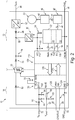
- Fig. 2 shows a schematic block diagram of an electrical network system, e.g. an electronic control unit (ECU), 10 according to the present invention, wherein the electrical network system 10 has a first supply voltage domain 12, a second supply voltage domain 14, and a transceiver device 100 according to the present invention for interfacing between the first and the second supply voltage domain 12, 14.
- ECU electronice control unit
- the electrical network system 10 shown in Fig. 2 corresponds to the electrical network system 10 shown in Fig. 1 , with a first exception that the conventional transceiver device 96, which is embodied as a 48V CAN transceiver in Fig. 1 , is replaced by a transceiver device 100 according to the invention, which is embodied in Fig. 2 likewise as a 48V CAN transceiver, and however according to the invention, and a second exception that the transceiver device 100 has some additional functional pins both in the first and the second supply voltage domain, a third exception that the electrical network system 10 has some additional elements that are described below.
- the transceiver device 100 has a first interface 110, a second interface 120, a first internal communication link 130 and a second internal communication link 170, wherein the internal communication links 130 and 170 bridge between the first and the second interface 110, 120.
- first and second internal communication links may be more than one first and second internal communication links, for example, a further first and second internal communication link for transmitting a mode signal (or a device mode indicating signal), for example from the second voltage supply domain to the first voltage supply domain, a still further first and second internal communication link for transmitting a wake signal, for example from the first voltage supply domain to the second voltage supply domain, and a still further first and second internal communication link for transmitting a device status information signal.
- a mode signal or a device mode indicating signal
- a wake signal for example from the first voltage supply domain to the second voltage supply domain
- a still further first and second internal communication link for transmitting a device status information signal.
- the first (high) supply voltage domain 12 and the second (low) supply voltage domain 14 are interfaced, independently and outside of the transceiver device 100, by a galvanic isolated flyback converter 70.
- a second (low) supply voltage terminal of the galvanic isolated flyback converter 70 is supplied by (or connected to) the low-voltage/second domain supply 72 via a fourth diode 80.
- a first (high) supply voltage terminal of the galvanic isolated flyback converter 70 connects via a second diode 76 to the first connection point 59, and hence to the 12V input of the second voltage converter 60.
- the first connection point 59 is buffered to high-voltage/first domain ground 56 via a third capacitor 78.
- the transceiver device 100 is for interfacing between at least two different voltage domains 12 and 14, which comprise namely the first supply voltage domain 12, which has a higher first supply voltage, and the second supply voltage domain 14, which has a lower second supply voltage.
- the transceiver device 100 has a first interface 110, which is supplied by the first supply voltage and is adapted to interface to at least one external first digital device 20 operating in the first supply voltage domain 12; and a second interface 120, which is supplied by the second supply voltage and is adapted to interface to an external communication bus 24 operating in the second supply voltage domain 14.
- the transceiver device 100 further has a first internal communication link 130, which is adapted to transfer transmit data, which are generatable by the external first digital device 20 operating in the first supply voltage domain 12, from the first interface 110 to the second interface 120; and a second internal communication link 170, which is adapted to transfer receive data, which may be supplied from the external communication bus 24 operating in the second supply voltage domain 14, from the second interface 120 to the first interface 110.
- the receive data may originate from a device that operates in the second supply voltage domain 14 and is connected to the communication bus 24.
- the first and the second internal communication links 130 and 170 together enable bidirectional transmission of transmit data and receive data between a digital device 30, for example the microcontroller unit (MCU) 32, operating in the first (high) supply voltage domain 12 and the communication bus 24, for example a CAN bus, operating in the second (low) supply voltage domain 14.
- a digital device for example the microcontroller unit (MCU) 32, operating in the first (high) supply voltage domain 12 and the communication bus 24, for example a CAN bus, operating in the second (low) supply voltage domain 14.
- MCU microcontroller unit
- the internal communication links 130, 170 are tolerant to ground offsets, common mode transients between the first supply voltage domain 12 (which may be embodied as the 12V/24V domain of the MHEV) and the second supply voltage domain 14 (which may be embodied as the 48V domain of the MHEV), and minimizes reverse currents into the CAN bus lines in loss of ground scenarios.
- the transceiver device 100 does not have nor needs a galvanic isolation barrier (see e.g. 98 in Fig. 1 ), for which one of the following methods are conventionally known: transformer, capacitor, or optocoupler. All these galvanic isolation barriers are expensive solutions, because according transceiver devices 96, e.g. CAN transceivers, as shown in Fig. 1 , consist of multiple integrated circuit dies in one package (multi-chip module package), or even worse and more expensive separate devices out of a transceiver device and one or more galvanic isolation devices may have to be applied.
- the transceiver device 100 has the first and second internal communication link 130 and 170, and may have more than one first and second internal communication links as mentioned above. As such, i.e. with all these components, the transceiver device 100 can be embodied as a monolithic integrated circuit.
- the monolithic integrated circuit including in particular the first and second internal communication links 130 and 170, can be implemented in silicon-on-insulator (SOI) technology, in particular high-voltage SOI technology.
- SOI silicon-on-insulator
- the transceiver device 100 has at least two ground pins 114, 124, which include a ground pin of the first supply voltage (or first domain ground, GND 48 ) 114 that is adapted to be connected to a ground potential 56 of the first voltage supply domain 12, and a ground pin of the second supply voltage (or second domain ground, GND 12/24 ) 124 that is adapted to be connected to a ground potential 74 of the second voltage supply domain 14.
- the transceiver device 100 may have a common mode and ground offset range from approximately ⁇ 3V to approximately ⁇ 70V.
- the first supply voltage may be substantially nominal 48V or greater.
- the second supply voltage may be substantially nominal 12V or substantially nominal 24V. This enables the transceiver device 100 to be applicable in automotive applications, e.g. in Mild Electric Hybrid Vehicles (MEHV).
- MEHV Mild Electric Hybrid Vehicles
- the first interface 110 has a transmit data input 116 adapted to receive the transmit data, e.g. from the first digital device 20 operating in the first supply voltage domain 12, and a receive data output 118 adapted to transmit the receive data, e.g. to a second digital device 22 operating in the first supply voltage domain 12.
- the first and the second digital devices 20 and 22 operating in the first supply voltage domain 12 may be a same digital device 30.
- the first and the second digital devices 20 and 22 operating in the first supply voltage domain 12 together may form a microcontroller unit 32.
- the second interface 120 has a CAN high pin 126 and a CAN low pin 128, which together are adapted to transmit the transmit data to and/or to receive the receive data from the CAN bus as the external communication bus 24 operating in the second supply voltage domain 14.
- the communication bus 24 may be selected from the group consisting of a CAN bus, a Flexray bus, a LIN bus, and an Ethernet.
- the first and the second internal communication link 130 and 170 may be based on differential voltage transmission, as will be explained further below with reference to Fig. 4 .
- the first and the second internal communication link 130 and 170 may be based on digital current loop transmission, as will be explained further below with reference to Figs. 5 and 6 .
- the transceiver device 100 may be embodied as 48V CAN transceiver. As such and as is shown in Fig. 2 , the transceiver device or 48V CAN transceiver 100 comprises in the first (high) voltage domain 12 the following pins: a supply input pin 112 for the first supply voltage (corresponding to V IO in Fig. 1 ), a ground pin 114 of the first supply voltage (or first domain ground, corresponding to GND 48 in Fig. 1 ), a transmit data input 116 (corresponding to TXD in Fig. 1 ), a receive data output 118 (corresponding to RXD in Fig. 1 ), and a mode port (not referenced) that connects via mode control signal line 38 to the microcontroller.
- a supply input pin 112 for the first supply voltage corresponding to V IO in Fig. 1
- a ground pin 114 of the first supply voltage or first domain ground, corresponding to GND 48 in Fig. 1
- a transmit data input 116 corresponding to TX
- the transceiver device 100 as such comprises in the second (low) voltage domain 14 the following pins: a supply input pin 122 for the second supply voltage (corresponding to BAT 12 in Fig. 1 ) that connects to the a low-voltage/second domain supply 72, corresponding to V BN12/24 in Fig. 1 ); a ground pin 124 of the second supply voltage (or second domain ground, corresponding to GND 12 in Fig. 1 ) that connects to the a low-voltage/second domain ground 74 (corresponding to GND 12/24 in Fig.
- At least one communication bus pin which is here (where the communication bus 24 is a CAN bus) embodied as a CAN high pin 126 and a CAN low pin 128; and a wake up port (not referenced) that connects to a wake-up voltage.
- the low-voltage/second domain supply 72 (V BN12/24 ) is connected to the supply input pin 122 for the second supply voltage (BAT 12 ) via a fifth diode 82.
- An output of the fifth diode 82 and/or the to the supply input pin 122 for the second supply voltage (BAT 12 ) is buffered to the second domain ground 124 via a third capacitor 84 and a fourth capacitor 86.
- the 48V CAN transceiver further comprises in the second (low) voltage domain 14 the pins VBUF (not referenced) and INHN (not referenced).
- the VBUF is connected to an external buffer capacitor (or fifth capacitor) 94, which is used to stabilize the internal voltage supply of the CAN transceiver IP within the 48V CAN transceiver device.
- the INHN output is typically an open drain output, which is used for switching on and off, depending on the 48V CAN transceiver mode, an external supply circuit or device to supply the microcontroller unit 32. In the embodiment illustrated in Fig. 2 , the INHN switches on and off the galvanic isolated flyback converter 70.
- the wake-up voltage is connected, in the embodiment illustrated in Fig. 2 , to the wake up port via a wake voltage line 92 comprising a first resistor 88, and to the second domain ground 124 via a second resistor 90.
- the WAKE pin can be used to detect a wake event, e.g. a rising edge on V WAKE . After detection of a wake event, the 48V CAN transceiver will switch on, via the INHN output, the supply for the microcontroller unit 32.
- the circuitry inside and outside the transceiver device 100 connected to the WAKE pin may vary a lot, depending on the wake source, i.e. the source of V WAKE .
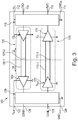
- Fig. 3 shows a schematic block diagram, and illustrates a core function, of a transceiver device 100 according to a first embodiment of the present invention, for interfacing between a first and a second supply voltage domain 12, 14.
- the transceiver device 100 has the first internal communication link 130, which comprises a first link transmitter 132, and a first link receiver 134, and which is capable to transfer the transmit data in the direction from the first interface 110 to the second interface 120.
- the transceiver device 100 further has the second internal communication link 170, which comprises a second link transmitter 172, and a second link receiver 174, and which is capable to transfer the receive data in the reverse direction from the second interface 120 to the first interface 110.
- Fig. 4 shows a schematic block diagram, and illustrates a core function, of a transceiver device 100 according to a second embodiment of the present invention, for interfacing between a first and a second supply voltage domain 12 and 14, wherein the first and the second internal communication links 130 and 170 use the principle of differential voltage transmission for the transmission of, respectively, the transmit data and receive data.
- the transceiver device 100 in respect of the transmission of transmit data and receive data, respectively, the first and the second internal communication link 130, 170 is indicated to be based on differential voltage transmission.
- the first internal communication link 130 is embodied a first differential voltage transmission link 140.
- the first link transmitter 132 is embodied as a first differential voltage transmitter 141, which operates with reference to, in particular is supplied by, the first supply voltage domain 12.
- the first differential voltage transmitter 141 is adapted to receive, via the first interface 110, the transmit data generated by the first digital device 20 operating in the first supply voltage domain 12, and is further adapted to generate and output a first differential voltage signal for transmitting the transmit data.
- the first link receiver 134 is embodied as a first differential voltage receiver 144, which operates with reference to, in particular is supplied by, the second supply voltage domain 14.
- the first differential voltage receiver 144 is adapted to receive the differential voltage signal transmitted by the first differential voltage transmitter 141, and is further adapted to transmit a first single-ended digital signal for transmitting the transmit data, via the second interface 120, to the external communication bus 24, which operates in the second supply voltage domain 14 and is embodied as CAN bus having a CAN high line 26 and a CAN low line 28.
- the first differential voltage transmitter 141 has a first switch-based H-bridge 142, which operates with reference to, in particular is supplied by, the first supply voltage domain 12, and the first differential voltage receiver 144 has a first voltage divider resistor ladder 145 and a first comparator 146, which operates with reference to, in particular is supplied by, the second supply voltage domain 14.
- the first switch-based H-bridge 142 comprises a first switch 142-1, a second switch 142-2, a third switch 142-3, and a fourth switch 142-4.
- the second switch 142-2 and the first switch 142-1 are connected in series, and the series connected second switch 142-2 and first switch 142-1 are connected between the first supply voltage Vio, which is supplied via the supply input pin 112, and the first domain ground GND 48 , which is supplied via the ground pin 114 of the first supply voltage.
- the fourth switch 142-4 and the third switch 142-3 are connected in series, and the series connected fourth switch 142-4 and third switch 142-3 are connected between the first supply voltage Vio, which is supplied via the supply input pin 112, and the first domain ground GND 48 , which is supplied via the ground pin 114 of the first supply voltage.
- the series connected second switch 142-2 and first switch 142-1 are connected in parallel to the series connected fourth switch 142-4 and third switch 142-3, between the first supply voltage V IO and first domain ground GND 48 .
- a first line 140-1 of the first differential communication link 140, or a first output of the first switch-based H-bridge 142 is connected to a connection point between the third switch 142-3 and the fourth switch 142-4.
- a second line 140-2 of the first communication link 140, or a second output of the first switch-based H-bridge 142 is connected to a connection point between the first switch 142-1 and the second switch 142-2.
- the first switch 142-1 and the third switch 142-3 are coupled in the sense that they are switched, i.e. opened and closed, simultaneously.
- the second switch 142-2 and the fourth switch 142-4 are coupled in the sense that they are switched, i.e. opened and closed, simultaneously.
- An input signal to the first switch-based H-bridge 142 switches, upon transition to a high state (or low state), the mutually coupled first switch 142-1 and third switch 142-3 simultaneously on and the mutually coupled second switch 142-2 and fourth switch 142-4 off.
- the input signal to the first switch-based H-bridge 142 switches, upon transition to a low state (or high state), the mutually coupled first switch 142-1 and third switch 142-3 simultaneously off and the mutually coupled second switch 142-2 and fourth switch 142-4 on.
- the first output line 140-1 of the first differential communication link 140 assumes the potential of the first domain ground (GND 48 ) 114, and the second output line 140-2 of the first differential communication link 140, assumes the potential of the first supply voltage (V IO ) 112.
- the first output line 140-1 of the first differential communication link 140 assumes the potential of the first supply voltage (V IO ) 112, and the second output line 140-2 of the first differential communication link 140, assumes the potential of the first domain ground (GND 48 ) 114.
- the first line 140-1 of the first differential communication link 140 and the second line 140-2 of the first differential communication link 140 always have an "opposite potential" relative to each other, and as such the first differential communication link 140 transmits a differential voltage, which carries the transmit data.
- the first voltage divider resistor ladder 145 has, connected in series, a first resistor 145-1 having substantially a second resistance value R2, a second resistor 145-2 having substantially a first resistance value R1, a third resistor 145-3 having substantially the first resistance value R1, and a fourth resistor 145-4 having substantially the second resistance value R2.
- the first differential voltage signal as output from the first switch-based H-bridge 142 via the first line 140-1 and the second line 140-2 of the first differential communication link 140, is applied across the series connection consisting of the first to fourth resistor 145-1 to 145-4. Then, a first auxiliary differential voltage signal is output by the first voltage divider resistor ladder 145 from between a first connection point 145-5 connected between the first and the second resistor 145-1 and 145-2 and a second connection point 145-6 connected between the third and the fourth resistor 145-3 and 145-4. A third connection point 145-7 connected between the second and the third resistor 145-2 and 145-3 is connected to the second domain ground (GND 12/24 ) 124.
- the first comparator 146 has an input 146-1, an inverting input 146-2, and an output 146-3, and receives the first auxiliary differential voltage signal as applied to its input 146-1 and to its inverting input 146-2.
- the first comparator 146 outputs from its output 146-3 a first single-ended digital signal, which carries the transmit data.
- the second internal communication link 170 is embodied a second differential voltage transmission link 180.
- the second link transmitter 172 is embodied as a second differential voltage transmitter 181, which operates with reference to, in particular is supplied by, the second supply voltage domain 14.
- the second differential voltage transmitter 181 is adapted to receive, via the second interface 120, the receive data, which are supplied from the external communication bus 24 operating in the second supply voltage domain 14, and is further adapted to generate and output a second differential voltage signal for transmitting the receive data.
- the second link receiver 174 is embodied as a second differential voltage receiver 184, which operates with reference to, in particular is supplied by, the first supply voltage domain 12.
- the second differential voltage receiver 184 is adapted to receive the differential voltage signal transmitted by the second differential voltage transmitter 181, and is further adapted to transmit a second single-ended digital signal for transmitting the receive data, via the first interface 110, to the second digital device 22 operating in the first supply voltage domain 12.
- the second differential voltage transmitter 181 has a second switch-based H-bridge 182, which operates with reference to, in particular is supplied by, the second supply voltage domain 14, and the second differential voltage receiver 184 has a first voltage divider resistor ladder 185 and a first comparator 186, which operates with reference to, in particular is supplied by, the first supply voltage domain 12.
- the second switch-based H-bridge 182 comprises a first switch 182-1, a second switch 182-2, a third switch 182-3, and a fourth switch 182-4.
- the first switch 182-1 and the second switch 182-2 are connected in series, and the series connected first switch 182-1 and second switch 182-2 are connected between the second supply voltage V BUF , which is supplied via the supply input pin 122, and the second domain ground GND 12/24 , which is supplied via the ground pin 124 of the second supply voltage.
- the third switch 182-3 and the fourth switch 182-4 are connected in series, and the series connected third switch 182-3 and fourth switch 182-4 are connected between the second supply voltage V BUF , which is supplied via the supply input pin 122, and the second domain ground GND 12/24 , which is supplied via the ground pin 124 of the second supply voltage.
- the series connected first switch 182-1 and second switch 182-2 are connected in parallel to the series connected third switch 182-3 and fourth switch 182-4, between second first supply voltage V BUF and second domain ground GND 12/24 .
- a first line 180-1 of the second differential communication link 180, or a first output of the second switch-based H-bridge 182 is connected to a connection point between the third switch 182-3 and the fourth switch 182-4.
- a second line 180-2 of the second differential communication link 180, or a second output of the second switch-based H-bridge 182 is connected to a connection point between the first switch 182-1 and the second switch 182-2.
- the first switch 182-1 and the third switch 182-3 are coupled in the sense that they are switched, i.e. opened and closed, simultaneously.
- the second switch 182-2 and the fourth switch 182-4 are coupled in the sense that they are switched, i.e. opened and closed, simultaneously.
- An input signal to the first switch-based H-bridge 182 switches, upon transition to a high state (or low state), the mutually coupled first switch 182-1 and third switch 182-3 simultaneously on and the mutually coupled second switch 182-2 and fourth switch 182-4 off.
- the input signal to the first switch-based H-bridge 182 switches, upon transition to a low state (or high state), the mutually coupled first switch 182-1 and third switch 182-3 simultaneously off and the mutually coupled second switch 142-2 and fourth switch 182-4 on.
- the first output line 180-1 of the second differential communication link 180 assumes the potential of the second domain ground (GND 12/24 ) 124, and the second output line 180-2 of the second differential communication link 180, assumes the potential of the first supply voltage (V BUF ) 122.
- the first output line 180-1 of the second differential communication link 180 assumes the potential of the second supply voltage (V BUF ) 122, and the second output line 180-2 of the second differential communication link 180, assumes the potential of the second domain ground (GND 12/24 ) 124.
- the first line 180-1 of the second differential communication link 180 and the second line 180-2 of the second differential communication link 180 always have an "opposite potential" relative to each other, and as such the second differential communication link 180 transmits a differential voltage, which carries the receive data.
- the second voltage divider resistor ladder 185 has, connected in series, a first resistor 185-1 having substantially a second resistance value R2, a second resistor 185-2 having substantially a first resistance value R1, a third resistor 185-3 having substantially the first resistance value, and a fourth resistor 185-4 having substantially the second resistance value.
- the second differential voltage signal as output from the second switch-based H-bridge 182, is applied across the series connection consisting of the first to fourth resistor 185-1 to 185-4. Then, a second auxiliary differential voltage signal is output by the second voltage divider resistor ladder 185 from between a first connection point 185-5 connected between the first and the second resistor 185-1 and 185-2 and a second connection point 185-6 connected between the third and the fourth resistor 185-3 and 185-4.
- a third connection point 185-7 connected between the second and the third resistor 185-2 and 185-3 is connected to the first domain ground (GND 48 ) 114.
- the second comparator 186 has an input 186-1, an inverting input 186-2, and an output 186-3, and receives the second auxiliary differential voltage signal as applied to its input 186-1 and to its inverting input 186-2.
- the second comparator 186 outputs from its output 186-3 a second single-ended digital signal, which carries the receive data.
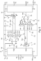
- Fig. 5 shows a schematic block diagram, and illustrates a core function, of a transceiver device 100 according to a third embodiment of the present invention, for interfacing between a first and a second supply voltage domain 12 and 14, wherein the first and the second internal communication links 130 and 170 use the principle of digital current loop transmission for the transmission of, respectively, the transmit data and receive data.
- the first internal communication link 130 is embodied as a first digital current loop transmission link 150, which has a first link transmitter 132 that is embodied a first transconductance transmitter 151.
- the first transconductance transmitter 151 operates with reference to, in particular is supplied by, the first supply voltage domain 12.
- the first transconductance transmitter 151 is adapted to receive, via the first interface 110, a first input voltage for carrying the transmit data generated by the first digital device 20 operating in the first supply voltage domain 12, and is further adapted to convert the first input voltage into, and output, a first differential current for transmitting the transmit data.
- the first differential current is in particular a two-way current, which is carried by the first line 150-1 and the second line 150-2 of the first digital current loop transmission link 150, to thereby form a two-way current loop, which is capable to represent dominant and recessive levels of a stream of transmit data.
- the first transconductance transmitter 151 may be based on an active H-bridge driver circuitry.
- the first link receiver 134 is embodied as a first digital differential current loop receiver 154, which operates with reference to, in particular is supplied by, the second supply voltage domain 14.
- the first digital differential current loop receiver 154 is adapted to receive the first differential current output, and is further adapted to convert this into, and output, a first single-ended digital signal for transmitting the transmit data, via the second interface 120, to the external communication bus 24 operating in the second supply voltage domain 14.
- the first digital differential current loop receiver 154 has a first voltage divider resistor ladder 155 and a first differential current loop voltage comparator 156, which operates with reference to, in particular is supplied by, the second supply voltage domain 14.
- the first voltage divider resistor ladder 155 has, connected in series, a first resistor 155-1 having substantially a second resistance value R2, a second resistor 155-2 having substantially a first resistance value R1, a third resistor 155-3 having substantially the first resistance value R1, and a fourth resistor 155-4 having substantially the second resistance value R2.
- the first differential current signal as output from the first transconductance transmitter 151, is applied across the series connection consisting of the first to fourth resistor 155-1 to 155-4. Then, a first auxiliary differential voltage signal is output by the first voltage divider resistor ladder 155 from between a first connection point 155-5 connected between the first and the second resistor 155-1 and 155-2 and a second connection point 155-6 connected between the third and the fourth resistor 155-3 and 155-4.
- a third connection point 155-7 between the second and the third resistor 155-2 and 155-3 may be connected to the second domain ground (GND 12/24 ) 124.
- the first differential current loop voltage comparator 156 has an input 156-1, an inverting input 156-2, and an output 156-3, and receives the first auxiliary differential voltage signal as applied to its input 156-1 and to its inverting input 156-2.
- the first differential current loop voltage comparator 156 outputs from its output 156-3 a first single-ended digital signal, which carries the transmit data.
- the transmit data are then further transmitted through the second interface 120 to the external communication bus 24 operating in the second supply voltage domain 14.
- the second internal communication link 170 is embodied as a second digital current loop transmission link 190, which has a second link transmitter 172 that is embodied as a second transconductance transmitter 191.
- the second transconductance transmitter 191 operates with reference to, in particular is supplied by, the second supply voltage domain 12. It is further adapted to receive, via the second interface 120, a second input voltage for carrying the receive data, which are supplied from the external communication bus 24 operating in the second supply voltage domain 14, and is further adapted to convert the second input voltage into, and output, a second differential, in particular two-way, current output for transmitting the receive data.
- the second differential current is in particular a two-way current, which is carried by the first line 190-1 and the second line 190-2 of the second digital current loop transmission link 190, to thereby form a two-way current loop, which is capable to represent dominant and recessive levels of a stream of receive data.
- the second transconductance transmitter 191 may be based on an active H-bridge driver circuitry.
- the second digital current loop transmission link 190 has a second link receiver 174 that is embodied as a second digital differential current loop receiver 194.
- the second digital differential current loop receiver 194 is adapted to receive the second differential current output, and is further adapted to convert this into, and output, a second single-ended digital signal for transmitting the receive data, via the first interface 110, to the second digital device 22 operating in the first supply voltage domain 12.
- the second digital differential current loop receiver 194 has a second voltage divider resistor ladder 195 and a second differential current loop voltage comparator 196, which operates with reference to, in particular is supplied by, the first supply voltage domain 12.
- the second voltage divider resistor ladder 195 has, connected in series, a first resistor 195-1 having substantially a second resistance value R2, a second resistor 195-2 having substantially a first resistance value R1, a third resistor 195-3 having substantially the first resistance value, and a fourth resistor 195-4 having substantially the second resistance value.
- the second differential current signal as output from the second transconductance transmitter 191, is applied across the series connection consisting of the first to fourth resistor 195-1 to 195-4. Then, a second auxiliary differential voltage signal is output by the second voltage divider resistor ladder 195 from between a first connection point 195-5 connected between the first and the second resistor 195-1 and 195-2 and a second connection point 195-6 connected between the third and the fourth resistor 195-3 and 195-4.
- a third connection point 195-7 between the second and the third resistor 195-2 and 195-3 may be connected to the first domain ground (GND 48 ) 114.
- the second differential current loop voltage comparator 196 has an input 196-1, an inverting input 196-2, and an output 196-3, and receives the first auxiliary differential voltage signal as applied to its input 196-1 and to its inverting input 196-2.
- the second differential current loop voltage comparator 196 outputs from its output 196-3 a second single-ended digital signal, which carries the receive data.
- the receive data are then further transmitted through the first interface 110 to the second digital device 22 operating in the first supply voltage domain 12.
- Fig. 6 shows a schematic block diagram, and illustrates a core function, of a transceiver device 100 according to the third embodiment of the present invention illustrated in Fig. 5 , showing details of the first and second transconductance transmitters 151, 191.
- the first transconductance transmitter 151 has a first branch having, connected in series, a first current source 151-1 adapted to generate a first electric current and a first switch 151-2, and a second branch having, connected in series, a second current source 151-3 adapted to generate a second electric current and a second switch 151-4.
- the first branch and the second branch are connected in parallel between a first connection point 152-1 and a second connection point 152-2.
- the second electric current is directed opposite to the first electric current.
- the first connection point 152-1 represents a first output that connects to a first output line 150-1 of the first digital current loop communication link 150
- the second connection point 152-2 represents a second output that connects to a second output line 150-2 of the first digital current loop communication link 150, which transfers the transmit data from the first interface 110 to the second interface 120.
- the second transconductance transmitter 191 has a first branch having, connected in series, a first current source 191-1 adapted to generate a first electric current and a first switch 191-2, and a second branch having, connected in series, a second current source 191-3 adapted to generate a second electric current and a second switch 191-4.
- the first branch and the second branch are connected in parallel between a first connection point 192-1 and a second connection point 192-2.
- the second electric current is directed opposite to the first electric current.
- the first connection point 192-1 represents a first output that connects to a first output line 190-1 of the second digital current loop communication link 190
- the second connection point 192-2 represents a second output that connects to a second output line 190-2 of the second digital current loop communication link 190, which transfers the receive data from the second interface 120 to the first interface 110.
Landscapes
- Engineering & Computer Science (AREA)
- Computer Networks & Wireless Communication (AREA)
- Signal Processing (AREA)
- Computer Hardware Design (AREA)
- Mechanical Engineering (AREA)
- Physics & Mathematics (AREA)
- Computing Systems (AREA)
- General Engineering & Computer Science (AREA)
- Mathematical Physics (AREA)
- Dc Digital Transmission (AREA)
Abstract
Description
- The invention relates to a transceiver device for interfacing between at least two different voltage domains, and to a method of interfacing between at least two different voltage domains.
- In the automotive industry, among others striving for CO2 emission reduction, Mild Electric Hybrid Vehicles (MHEVs) have been introduced, which have two board net voltage domains, in particular 12V or 24V on the one hand and 48V on the other hand. In such MHEVs, the electric high-power applications including an electric motor, such as e.g. an electric starter generator, of the vehicle, which are typically operative in the range of 1 to 15 kW, are connected to the 48V board net.
- The Controller Area Network (CAN) bus is often used in automotive and industrial automation applications. The CAN bus system was developed in 1983 by the company Bosch and presented publically in 1986 together with the company Intel. The CAN bus has evolved to a bus standard in automotive and industrial automation applications, and is described in ISO 11898. A CAN bus can support bit-rates up to 8 Mbps in the case of the extension CAN FD, which was developed in 2011 and released in 2012 by the company Bosch, if the network topology is correctly terminated.
- In MHEVs, 12V board net electronic control units (ECUs) and 48V board net units are connected to a same Controller Area Network (CAN) bus network. To enable such mixed 12V/48V CAN networks, a CAN transceiver of ECUs operating at 48V must tolerate common mode difference and have provisions to limit a maximum potential voltage on CAN bus lines and reverse currents into CAN bus lines.
- In mixed 12V/48V CAN networks, ECUs operating at 48V typically have four power connector pins:
VBN48: 48V board net connector (e.g. Kl. 40), GND48: ground connector of 48V board net (e.g. Kl. 41), VBN12/24: 12V or 24V board net connector (e.g. Kl. 30), and GND12/24: ground connector of 12V or 24V board net (e.g. Kl. 31) - A 48V CAN transceiver is typically connected between the 12V/24V voltage supply domain and the 48V voltage supply domain, as is illustrated in
Fig. 1 and as is described further below. - In MHEVs, the grounds of both board net domains (supply voltage domains) are somewhere connected. The position of this shared ground connections depends on the car manufacturer. Although the grounds are somewhere connected, automotive transients in combination with the (long) wiring harness cause ground offsets and common mode transients between the ECU ground pins, viz. GND12/24 and GND48. This could result in communication disturbances. Furthermore, loss of ground scenarios are possible, which can lead to high voltage differences between GND12/24 and GND48.
- To overcome these problems in current 48V ECUs, CAN transceivers with high-voltage galvanic isolation are used to handle with, or connect to, both board net domains. As galvanic isolation barrier, the following methods are used: (voltage) transformer, capacitor, or optocoupler. All these known galvanic isolation barriers are expensive solutions, because such CAN transceivers consist of multiple integrated circuit dies in one package (multi-chip module package). Or even worse, a discrete solution comprising a separate CAN transceiver device and one or more separate galvanic isolation devices may be applied.
- Although the above description of the background of the invention relates to state of the art ECUs operating at 48V, 48V CAN transceivers, and mixed 12V/48V or 24V/48V CAN networks, which have been developed in the automotive industry in respect of MHEVs, and the present invention - as will be disclosed in the following - has been developed initially in this field of technology, the present invention can be generalized to be applicable in interfacing to other bus systems, such as a Local Interconnect Network (LIN) bus (as described in ISO 17987) and a FlexRay bus (as described in ISO 17458-1 to 17458-5), or more generally to a communication medium, including e.g. Ethernet, in interfacing between supply voltage domains different having different supply voltages than 12/24V and 48V (as used in the automotive industry).
- The present invention relates to a transceiver device for interfacing between at least two different voltage domains, and to a method of interfacing between at least two different voltage domains.
- It is a general object of the present invention to provide a device for digitally interfacing and a method of digitally interfacing between a high-voltage supply domain and a low-voltage supply domain, which reduces or eliminates the impact(s) of ground offset, common mode transients and loss of ground scenarios without galvanic isolation, so as to enable a solution with a single integrated circuit die. Further objects of the present invention comprise a provision of common mode tolerance, and measures against high voltages and currents crossing from one domain to the other.
- This object is solved by the subjects having the features according to the independent patent claims. Preferred and advantageous embodiments are described in the dependent claims. In particular, this object is solved by a transceiver device according to the appended independent claim 1, and by a method according to the appended independent claim 19. Further embodiment examples of the invention are described in the dependent claims.
- According to a first exemplary embodiment of the present invention, there is provided a transceiver device for interfacing between at least two different voltage domains, namely a first supply voltage domain having a higher first supply voltage and a second supply voltage domain having a lower second supply voltage, wherein the transceiver device has:
- a first interface, which is supplied by the first supply voltage and is adapted to interface to at least one external first digital device operating in the first supply voltage domain;
- a second interface, which is supplied by the second supply voltage and is adapted to interface to an external communication bus operating in the second supply voltage domain;
- a first internal communication link, which is adapted to transfer transmit data, which are generatable (or can be generated) by the external first digital device operating in the first supply voltage domain, from the first interface to the second interface, and
- a second internal communication link, which is adapted to transfer transmit data, which are supplyable (or can be supplied, or can be provided) from the external communication bus operating in the second supply voltage domain, from the second interface to the first interface. Herein, in particular, the receive data may originate from a device that operates in the second supply voltage domain and is connected to the communication bus.
- By providing the first and second internal communication for transmitting both transmit and receive data, for duplex transmission, the impacts of ground offset, common mode transients, and loss of ground scenarios can be solved without provision of galvanic isolation. This in turn enables the following advantageous embodiment examples.
- The transceiver device according to the first exemplary embodiment of the present invention may have more than one first and second internal communication links, for example, a further first and second internal communication link for transmitting a device mode indicating signal, and a still further first and second internal communication link for transmitting a device status information signal.
- In an advantageous embodiment example of the present invention, the transceiver device, including the first interface, the second interface, the first internal communication link, and the second internal communication link, and in particular further first and second internal communication links, may be embodied as a monolithic integrated circuit. In a particular advantageous embodiment example thereof, the monolithic integrated circuit may be implemented in silicon-on-insulator (SOI) technology.
- In an embodiment example of the present invention, the transceiver device may further have at least two ground pins, including a first ground pin adapted to be connected to a ground potential of the first voltage supply domain, and a second ground pin adapted to be connected to a ground potential of the second voltage supply domain.
- In an embodiment example of the present invention, the transceiver device may further have a common mode and ground offset range that is in a range starting from more than approximately ±3V, but not exceeding approximately ±70V.
- In an embodiment example of the present invention, the first supply voltage is substantially nominal 48V or greater. In an embodiment example of the present invention, the second supply voltage is substantially nominal 12V or substantially nominal 24V.
- In an embodiment example of the present invention, the first interface may have: a transmit data input adapted to receive the transmit data, e.g. from the first digital device operating in the first supply voltage domain, and a receive data output adapted to transmit the receive data, e.g. to a second digital device operating in the first supply voltage domain.
- In a further development of this embodiment example, the first and the second digital device operating in the first supply voltage domain may be a same digital device, and/or the first and the second digital device operating in the first supply voltage domain may together form a microcontroller unit.
- In an embodiment example of the present invention, the second interface may have: at least one communication bus pin adapted to transmit the transmit data to and/or receive the receive data from the external communication bus operating in the second supply voltage domain.
- In a further development of this embodiment example, the external communication bus operating in the second supply voltage domain may be selected from the group consisting of a CAN bus, a Flexray bus, a LIN bus, and an Ethernet.
- In a first particular embodiment example of the present invention, in respect of the transmission of transmit data and receive data, respectively, the first and the second internal communication link may be based on differential voltage transmission.
- In a second particular embodiment example of the present invention, which is alternative to the first particular embodiment example of the present invention as described hereinbefore, in respect of the transmission of transmit data and receive data, respectively, the first and the second internal communication link are based on digital current loop transmission.
- By embodying the first and the second internal communication link either as being based on differential voltage transmission or being are based on digital current loop transmission, the internal communication links provide tolerance to ground offset, common mode transients and minimize reverse currents into the lines of the second (lower) supply voltage domain in loss of ground scenarios.
- In a further development of the first particular embodiment example of the present invention, the first internal communication link may comprise a first differential voltage transmitter and a first differential voltage receiver. The first differential voltage transmitter may operate with reference to, in particular may be supplied by, the first supply voltage domain, and may be adapted to receive, via the first interface, the transmit data generated by the first digital device operating in the first supply voltage domain, and to generate and output a first differential voltage signal for transmitting the transmit data. The first differential voltage receiver may operate with reference to, in particular is supplied by, the second supply voltage domain, and may be adapted to receive the differential voltage signal transmitted by the first differential voltage transmitter, and to transmit a first single-ended digital signal for transmitting the transmit data, via the second interface, to the external communication bus operating in the second supply voltage domain.
- In a corresponding further development of the first particular embodiment example of the present invention, the second internal communication link may comprise a second differential voltage transmitter and a second differential voltage receiver. The second differential voltage transmitter may operate with reference to, in particular may be supplied by, the second supply voltage domain, and may be adapted to receive, via the second interface, the receive data supplyable from the external communication bus operating in the second supply voltage domain, and to generate and output a second differential voltage signal for transmitting the receive data. The second differential voltage receiver may operate with reference to, in particular may be supplied by, the first supply voltage domain, and may be adapted to receive the differential voltage signal transmitted by the second differential voltage transmitter, and to transmit a second single-ended digital signal for transmitting the receive data, via the first interface, to the second digital device operating in the first supply voltage domain.
- In a corresponding still further development of the first particular embodiment example of the present invention, the first differential voltage transmitter may have a first switch-based H-bridge, which may operate with reference to, in particular may be supplied by, the first supply voltage domain, and the first differential voltage receiver may have a first voltage divider resistor ladder and a first comparator, which operates with reference to, in particular is supplied by, the second supply voltage domain. The first voltage divider resistor ladder may have, connected in series, a first resistor having substantially a second resistance value, a second resistor having substantially a first resistance value, a third resistor having substantially the first resistance value, and a fourth resistor having substantially the second resistance value. The ratio between the first resistance value and the second resistance value can be determined from the following equation:

- The first differential voltage signal, as output from the first switch-based H-bridge, may be applied across the series connection consisting of the first to fourth resistor. A first auxiliary differential voltage signal may be output by the first voltage divider resistor ladder from between a first connection point connected between the first and the second resistor and a second connection point connected between the third and the fourth resistor. A third connection point connected between the second and the third resistor may be connected to the second domain ground. The first comparator has an input, an inverting input, and an output, and may receive the first auxiliary differential voltage signal as applied to its input and to its inverting input, and may output from its output the first single-ended digital signal.
- In a corresponding still further development of the first particular embodiment example of the present invention, the second differential voltage transmitter may have a second switch-based H-bridge, which may operate with reference to, in particular is supplied by, the second supply voltage domain, and the second differential voltage receiver may have a second voltage divider resistor ladder and a second comparator, which may operate with reference to, in particular is supplied by, the first supply voltage domain. The second voltage divider resistor ladder may have, connected in series, a first resistor having substantially a second resistance value, a second resistor having substantially a first resistance value, a third resistor having substantially the first resistance value, and a fourth resistor having substantially the second resistance value. The ratio between the first resistance value and the second resistance value can be determined from the following equation:

- The second differential voltage signal, as output from the second switch-based H-bridge, may be applied across the series connection consisting of the first to fourth resistor. A second auxiliary differential voltage signal may be output by the second voltage divider resistor ladder from between a first connection point connected between the first and the second resistor and a second connection point connected between the third and the fourth resistor. A third connection point connected between the second and the third resistor may be connected to the first domain ground. The second comparator has an input, an inverting input, and an output, and may receive the second auxiliary differential voltage signal as applied to its input and to its inverting input, and may output from its output the second single-ended digital signal.
- As stated already above, in a second particular embodiment example of the present invention, which is alternative to the first particular embodiment example as described hereinbefore, in respect of the transmission of transmit data and receive data, respectively, the first and the second internal communication link are based on digital current loop transmission.
- In a further development of the second particular embodiment example of the present invention, the first internal communication link may comprise a first transconductance transmitter and a first digital differential current loop receiver. The first transconductance transmitter may operate with reference to, in particular may be supplied by, the first supply voltage domain, and may be adapted to receive, via the first interface, a first input voltage for carrying the transmit data generated by the first digital device operating in the first supply voltage domain, and to convert the first input voltage into, and output, a first differential current output for transmitting the transmit data. The first digital differential current loop receiver may operate with reference to, in particular may be supplied by, the second supply voltage domain, and may be adapted to receive the first differential current output, and to convert this into, and output, a first single-ended digital signal for transmitting the transmit data, via the second interface, to the external communication bus operating in the second supply voltage domain.
- In a corresponding further development of the second particular embodiment example of the present invention, the second internal communication link may comprise a second transconductance transmitter and a second digital differential current loop receiver. The second transconductance transmitter may operate with reference to, in particular may be supplied by, the second supply voltage domain, and may be adapted to receive, via the second interface, a second input voltage for carrying the receive data supplyable from the external communication bus operating in the second supply voltage domain, and to convert the second input voltage into, and output, a second differential current output for transmitting the receive data. The second digital differential current loop receiver may operate with reference to, in particular may be supplied by, the first supply voltage domain, and may be adapted to receive the second differential current output, and to convert this into, and output, a second single-ended digital signal for transmitting the receive data, via the first interface, to the second digital device operating in the first supply voltage domain.
- In the corresponding still further development of the second particular embodiment example of the present invention, the first transconductance transmitter has a first branch having, connected in series, a first current source adapted to generate a first electric current and a first switch, and a second branch having, connected in series, a second current source adapted to generate a second electric current and a second switch. The first branch and the second branch are connected in parallel between a first connection point and a second connection point. The second electric current is directed opposite to the first electric current. The first connection point represents a first output that connects to a first line of the first internal communication link, and the second connection point represents a second output that connects to a second line of the first internal communication link.
- The first digital differential current loop receiver has a first voltage divider resistor ladder and a first differential current loop voltage comparator, which operates with reference to, in particular is supplied by, the second supply voltage domain. The first voltage divider resistor ladder has, connected in series, a first resistor having substantially a second resistance value, a second resistor having substantially a first resistance value, a third resistor having substantially the first resistance value, and a fourth resistor having substantially the second resistance value.
- The first differential current, Il_loop, signal, as output from the first transconductance transmitter, is applied across the series connection consisting of the first to fourth resistor. A first auxiliary differential voltage, V1_aux, signal is output by the first voltage divider resistor ladder from between a first connection point connected between the first and the second resistor and a second connection point connected between the third and the fourth resistor. A third connection point connected between the second and the third resistor may be connected to the second domain ground. The first differential current loop voltage comparator has an input, an inverting input, and an output, and receives the first auxiliary differential voltage signal as applied to its input and to its inverting input, and outputs from its output the first single-ended digital signal.
- A first voltage, VI, generated by the first differential current, Il_loop, flowing across the series connection consisting of the first to fourth resistors and the first auxiliary voltage, V1_aux, can be determined from the following equations:


- The first transconductance transmitter has a first branch having, connected in series, a first current source adapted to generate a first electric current and a first switch, and a second branch having, connected in series, a second current source adapted to generate a second electric current and a second switch. The first branch and the second branch are connected in parallel between a first connection point and a second connection point. The second electric current is directed opposite to the first electric current. The first connection point represents a first output that connects to a first line of the second internal communication link, and the second connection point represents a second output that connects to a second line of the second internal communication link.
- The second digital differential current loop receiver has a second voltage divider resistor ladder and a second differential current loop voltage comparator, which operates with reference to, in particular is supplied by, the second supply voltage domain. The second voltage divider resistor ladder has, connected in series, a first resistor having substantially a second resistance value, a second resistor having substantially a first resistance value, a third resistor having substantially the first resistance value, and a fourth resistor having substantially the second resistance value.
- The second differential current, I2_loop, signal, as output from the second transconductance transmitter, is applied across the series connection consisting of the first to fourth resistor. A second auxiliary differential voltage, V2_aux, signal is output by the second voltage divider resistor ladder from between a first connection point connected between the first and the second resistor and a second connection point connected between the third and the fourth resistor. A third connection point connected between the second and the third resistor may be connected to the first domain ground. The second differential current loop voltage comparator has an input, an inverting input, and an output, and receives the first auxiliary differential voltage signal as applied to its input and to its inverting input, and outputs from its output the first single-ended digital signal.
- A second voltage, V2, generated by the second differential current, I2_loop, flowing across the series connection consisting of the first to fourth resistors and the second auxiliary voltage, V2_aux, can be determined from the following equations:


- According to a second exemplary embodiment example of the present invention, there is provided an electrical network system, in particular an electronic control unit (ECU), having a higher first supply voltage domain and a lower second supply voltage domain, and a transceiver device according to the first exemplary embodiment example of the present invention and as described above, for interfacing between the first and the second supply voltage domains.
- According to a third exemplary embodiment example of the present invention, there is provided a vehicle having an electrical network system, in particular an electronic control unit (ECU), according to the second exemplary embodiment example of the present invention.
- According to a fourth exemplary embodiment example of the present invention, there is provided a method of interfacing between at least two different voltage domains, namely a first supply voltage domain having a higher first supply voltage and a second supply voltage domain having a lower second supply voltage, wherein the method uses a transceiver device having a first interface, a second interface, a first internal communication link, and a second internal communication link. The method has the following steps:
- supplying the first interface by the first supply voltage, and interfacing by the first interface to at least one external first digital device operating in the first supply voltage domain;
- supplying the second interface by the second supply voltage, and interfacing by the second interface to an external communication bus operating in the second supply voltage domain;
- transferring transmit data, which are generated by the external first digital device operating in the first supply voltage domain, through the first interface, via the first internal communication link to the second interface, and in particular further to the external communication bus operating in the second supply voltage domain; and
- transferring receive data, which are supplied from the external communication bus operating in the second supply voltage domain, through the second interface, via the second internal communication link to the first interface, and in particular further to an external second digital device operating in the first supply voltage domain. Herein, in particular, the receive data may originate from a device that operates in the second supply voltage domain and is connected to the communication bus.
- In a first particular embodiment example of the present invention, the method may further comprise operating the first and the second internal communication link in a differential voltage transmission mode.
- In a second particular embodiment example of the present invention, which is alternative to the first particular embodiment example of the present invention, the method may further comprise operating the first and the second internal communication link in a digital current loop transmission mode.
- In an embodiment example of the present invention, the transceiver device, including the first interface, the second interface, the first internal communication link, and the second internal communication link, may be embodied as a monolithic integrated circuit. In an advantageous embodiment example thereof, the monolithic integrated circuit may be implemented in silicon-on-insulator (SOI) technology.
- In an embodiment example of the present invention, the transceiver device may further have at least two ground pins, including a first ground pin adapted to be connected to a ground potential of the first voltage supply domain, and a second ground pin adapted to be connected to a ground potential of the second voltage supply domain.
- In an embodiment example of the present invention, the transceiver device may further have a common mode and ground offset range that is in a range starting from more than approximately ±3V, but not exceeding approximately ±70V.
- In an embodiment example of the present invention, the first supply voltage is substantially nominal 48V or greater. In an embodiment example of the present invention, the second supply voltage is substantially nominal 12V or substantially nominal 24V.
- In the following, exemplary embodiment examples of the present invention are described in detail with reference to the following drawings.
-
Fig. 1 shows a schematic block diagram of an electrical network system, e.g. an electronic control unit (ECU), having a first supply voltage domain, a second supply voltage domain, and a transceiver device, which has a galvanic isolation barrier in a conventional manner, for interfacing between the first and the second supply voltage domain. -
Fig. 2 shows a schematic block diagram of an electrical network system, e.g. an electronic control unit (ECU), according to the present invention, wherein the system has a first supply voltage domain, a second supply voltage domain, and a transceiver device according to the present invention for interfacing between the first and the second supply voltage domain. -
Fig. 3 shows a schematic block diagram, and illustrates a core function, of a transceiver device according to a first embodiment of the present invention, for interfacing between a first and a second supply voltage domain. -
Fig. 4 shows a schematic block diagram, and illustrates a core function, of a transceiver device according to a second embodiment of the present invention, for interfacing between a first and a second supply voltage domain. -
Fig. 5 shows a schematic block diagram, and illustrates a core function, of a transceiver device according to a third embodiment of the present invention, for interfacing between a first and a second supply voltage domain. -
Fig. 6 shows a schematic block diagram, and illustrates a core function, of a transceiver device according to the third embodiment of the present invention illustrated inFig. 5 , showing details of the first and second transconductance transmitters. - For reasons of conciseness, features, which will be described with respect a particular figure, may not be described again, if they appear likewise or similarly in another figure. Similar or identical elements in different figures are provided with same reference numerals.
-
Fig. 1 shows a schematic block diagram of an electrical network system, e.g. an electronic control unit (ECU), 10 having a firstsupply voltage domain 12, a secondsupply voltage domain 14, and atransceiver device 96, which has agalvanic isolation barrier 98 in a conventional manner, for interfacing between the first and the secondsupply voltage domain - By way of example, the
electrical network system 10 is a mixed 12V/48V or 24V/48V CAN network in a MHEV (not shown), thetransceiver device 96 is a 48V CAN transceiver of the MHEV, the first supply voltage is substantially nominal 48V and the second supply voltage is substantially nominal 12V or 24V in the MHEV. The48V CAN transceiver 96 has, in a conventional manner, agalvanic isolation barrier 98, which may be embodied according to one of the following methods: (voltage) transformer, capacitor, or optocoupler. - The first supply voltage domain (or high-voltage supply domain) 12 is supplied by a first (or high) supply voltage via a pair of
pins - The second supply voltage domain (or low-voltage supply domain) 14 is supplied by a second (or low) supply voltage via a pair of
pins - The
electrical network system 10 of the MHEV comprises, in the first (high)supply voltage domain 12, an electric motor, such as e.g. an electric starter generator, 50, a first voltage converter 52 (viz. 48V/12V), a second voltage converter (viz. 12V/VDD1), amicrocontroller unit 32 for controlling among others the operation of theelectric motor 50 via a driving line comprising a gate driver unit (GDU) 42, apower stage 46 for driving theelectric motor 50, and theelectric motor 50. - A 48V input of the a
first voltage converter 52 is connected to the a high-voltage/first domain supply 54 (VBN48). A 12V output of thefirst voltage converter 52 is connected to afirst connection point 59, which is also connected to a 12V input of thesecond voltage converter 60. A VDD1 (for example, 5V) output of thesecond voltage converter 60 is connected to a voltage supply input of themicrocontroller 32. Themicrocontroller 32 outputs, among others, control signals via a firstcontrol signal line 40 to a control input of theGDU 42. TheGDU 42 outputs, control signals via a secondcontrol signal line 44 to a control input of thepower stage 46. Thepower stage 46 outputs via adrive signal line 48 high-power driving voltages and driving currents for driving theelectric motor 50 of the MHEV. - The second supply voltage domain (or low-voltage supply domain) 14 is supplied by a second (or low) supply voltage via a pair of
pins - The
electrical network system 10 of the MHEV comprises, in the second (low)supply voltage domain 14, aCAN bus 24, which comprises a CAN bushigh line 26 and a CAN buslow line 28, for connecting to various ECUs and devices connected to the second (low)supply voltage domain 14. - The
transceiver device 96, which is embodied inFig. 1 as a conventional 48V CAN transceiver, as such, comprises in the first (high)voltage domain 12 the following pins:VDD1, TXD, RXD, and GND48. Furthermore, the conventional 48V CAN transceiver, as such comprises in the second (low)voltage domain 14 the following pins: VDD2, CANH, CANL, and GND12. These pins are similar in function, and correspond to the pins of the 48V CAN transceiver shown inFig. 2 , which exemplifies atransceiver device 100 according to the invention, and which is described further below with reference toFig. 2 . - The conventional 48V CAN
transceiver 96 has a galvanic isolation between the pins in the first (high)voltage domain 12 and the pins in the second (low)voltage domain 14. The galvanic isolation barrier may be implemented to comprise one of a galvanic isolation transformer, a galvanic isolation capacitor, or a galvanic isolation optocoupler. -
Fig. 2 shows a schematic block diagram of an electrical network system, e.g. an electronic control unit (ECU), 10 according to the present invention, wherein theelectrical network system 10 has a firstsupply voltage domain 12, a secondsupply voltage domain 14, and atransceiver device 100 according to the present invention for interfacing between the first and the secondsupply voltage domain - The
electrical network system 10 shown inFig. 2 corresponds to theelectrical network system 10 shown inFig. 1 , with a first exception that theconventional transceiver device 96, which is embodied as a 48V CAN transceiver inFig. 1 , is replaced by atransceiver device 100 according to the invention, which is embodied inFig. 2 likewise as a 48V CAN transceiver, and however according to the invention, and a second exception that thetransceiver device 100 has some additional functional pins both in the first and the second supply voltage domain, a third exception that theelectrical network system 10 has some additional elements that are described below. - Contrary to the transceiver (viz. the 48V CAN transceiver) 96 shown in
Fig. 1 and instead of having agalvanic isolation barrier 98, thetransceiver device 100 according to the present invention as illustrated inFig. 2 has afirst interface 110, asecond interface 120, a firstinternal communication link 130 and a secondinternal communication link 170, wherein theinternal communication links second interface - There may be more than one first and second internal communication links, for example, a further first and second internal communication link for transmitting a mode signal (or a device mode indicating signal), for example from the second voltage supply domain to the first voltage supply domain, a still further first and second internal communication link for transmitting a wake signal, for example from the first voltage supply domain to the second voltage supply domain, and a still further first and second internal communication link for transmitting a device status information signal.
- The first (high)
supply voltage domain 12 and the second (low)supply voltage domain 14 are interfaced, independently and outside of thetransceiver device 100, by a galvanicisolated flyback converter 70. A second (low) supply voltage terminal of the galvanicisolated flyback converter 70 is supplied by (or connected to) the low-voltage/second domain supply 72 via afourth diode 80. A first (high) supply voltage terminal of the galvanicisolated flyback converter 70 connects via asecond diode 76 to thefirst connection point 59, and hence to the 12V input of thesecond voltage converter 60. Thefirst connection point 59 is buffered to high-voltage/first domain ground 56 via athird capacitor 78. - The
transceiver device 100, as illustrated inFig. 2 , is for interfacing between at least twodifferent voltage domains supply voltage domain 12, which has a higher first supply voltage, and the secondsupply voltage domain 14, which has a lower second supply voltage. Thetransceiver device 100 has afirst interface 110, which is supplied by the first supply voltage and is adapted to interface to at least one external firstdigital device 20 operating in the firstsupply voltage domain 12; and asecond interface 120, which is supplied by the second supply voltage and is adapted to interface to anexternal communication bus 24 operating in the secondsupply voltage domain 14. - The
transceiver device 100, as illustrated inFig. 2 , further has a firstinternal communication link 130, which is adapted to transfer transmit data, which are generatable by the external firstdigital device 20 operating in the firstsupply voltage domain 12, from thefirst interface 110 to thesecond interface 120; and a secondinternal communication link 170, which is adapted to transfer receive data, which may be supplied from theexternal communication bus 24 operating in the secondsupply voltage domain 14, from thesecond interface 120 to thefirst interface 110. The receive data may originate from a device that operates in the secondsupply voltage domain 14 and is connected to thecommunication bus 24. - The first and the second
internal communication links supply voltage domain 12 and thecommunication bus 24, for example a CAN bus, operating in the second (low)supply voltage domain 14. - The
internal communication links - The
transceiver device 100 according to the invention does not have nor needs a galvanic isolation barrier (see e.g. 98 inFig. 1 ), for which one of the following methods are conventionally known: transformer, capacitor, or optocoupler. All these galvanic isolation barriers are expensive solutions, because accordingtransceiver devices 96, e.g. CAN transceivers, as shown inFig. 1 , consist of multiple integrated circuit dies in one package (multi-chip module package), or even worse and more expensive separate devices out of a transceiver device and one or more galvanic isolation devices may have to be applied. - Instead, the
transceiver device 100 according to the invention has the first and secondinternal communication link transceiver device 100 can be embodied as a monolithic integrated circuit. - With advantage, the monolithic integrated circuit, including in particular the first and second
internal communication links - It is noted that the
transceiver device 100 has at least twoground pins ground potential 56 of the firstvoltage supply domain 12, and a ground pin of the second supply voltage (or second domain ground, GND12/24) 124 that is adapted to be connected to aground potential 74 of the secondvoltage supply domain 14. As such, thetransceiver device 100 may have a common mode and ground offset range from approximately ±3V to approximately ±70V. - The first supply voltage may be substantially nominal 48V or greater. The second supply voltage may be substantially nominal 12V or substantially nominal 24V. This enables the
transceiver device 100 to be applicable in automotive applications, e.g. in Mild Electric Hybrid Vehicles (MEHV). - As is further illustrated in
Fig. 2 , thefirst interface 110 has a transmitdata input 116 adapted to receive the transmit data, e.g. from the firstdigital device 20 operating in the firstsupply voltage domain 12, and a receivedata output 118 adapted to transmit the receive data, e.g. to a seconddigital device 22 operating in the firstsupply voltage domain 12. Herein, the first and the seconddigital devices supply voltage domain 12 may be a same digital device 30. In addition or alternatively, the first and the seconddigital devices supply voltage domain 12 together may form amicrocontroller unit 32. - As is still further illustrated in
Fig. 2 , thesecond interface 120 has a CANhigh pin 126 and a CANlow pin 128, which together are adapted to transmit the transmit data to and/or to receive the receive data from the CAN bus as theexternal communication bus 24 operating in the secondsupply voltage domain 14. Thecommunication bus 24 may be selected from the group consisting of a CAN bus, a Flexray bus, a LIN bus, and an Ethernet. - In the
transceiver device 100 according to the invention, in respect of the transmission of transmit data and receive data, respectively, the first and the secondinternal communication link Fig. 4 . - Alternatively, in the
transceiver device 100 according to the invention, in respect of the transmission of transmit data and receive data, respectively, the first and the secondinternal communication link Figs. 5 and6 . - The
transceiver device 100 may be embodied as 48V CAN transceiver. As such and as is shown inFig. 2 , the transceiver device or48V CAN transceiver 100 comprises in the first (high)voltage domain 12 the following pins: asupply input pin 112 for the first supply voltage (corresponding to VIO inFig. 1 ), aground pin 114 of the first supply voltage (or first domain ground, corresponding to GND48 inFig. 1 ), a transmit data input 116 (corresponding to TXD inFig. 1 ), a receive data output 118 (corresponding to RXD inFig. 1 ), and a mode port (not referenced) that connects via modecontrol signal line 38 to the microcontroller. - Furthermore, the
transceiver device 100 as such comprises in the second (low)voltage domain 14 the following pins: asupply input pin 122 for the second supply voltage (corresponding to BAT12 inFig. 1 ) that connects to the a low-voltage/second domain supply 72, corresponding to VBN12/24 inFig. 1 ); aground pin 124 of the second supply voltage (or second domain ground, corresponding to GND12 inFig. 1 ) that connects to the a low-voltage/second domain ground 74 (corresponding to GND12/24 inFig. 1 ); at least one communication bus pin, which is here (where thecommunication bus 24 is a CAN bus) embodied as a CANhigh pin 126 and a CANlow pin 128; and a wake up port (not referenced) that connects to a wake-up voltage. - The low-voltage/second domain supply 72 (VBN12/24) is connected to the
supply input pin 122 for the second supply voltage (BAT12) via afifth diode 82. An output of thefifth diode 82 and/or the to thesupply input pin 122 for the second supply voltage (BAT12) is buffered to thesecond domain ground 124 via athird capacitor 84 and afourth capacitor 86. - The 48V CAN transceiver further comprises in the second (low)
voltage domain 14 the pins VBUF (not referenced) and INHN (not referenced). The VBUF is connected to an external buffer capacitor (or fifth capacitor) 94, which is used to stabilize the internal voltage supply of the CAN transceiver IP within the 48V CAN transceiver device. The INHN output is typically an open drain output, which is used for switching on and off, depending on the 48V CAN transceiver mode, an external supply circuit or device to supply themicrocontroller unit 32. In the embodiment illustrated inFig. 2 , the INHN switches on and off the galvanicisolated flyback converter 70. - The wake-up voltage is connected, in the embodiment illustrated in
Fig. 2 , to the wake up port via awake voltage line 92 comprising afirst resistor 88, and to thesecond domain ground 124 via asecond resistor 90. While the 48V CAN transceiver is in a low power mode, the WAKE pin can be used to detect a wake event, e.g. a rising edge on VWAKE. After detection of a wake event, the 48V CAN transceiver will switch on, via the INHN output, the supply for themicrocontroller unit 32. The circuitry inside and outside thetransceiver device 100 connected to the WAKE pin may vary a lot, depending on the wake source, i.e. the source of VWAKE. -
Fig. 3 shows a schematic block diagram, and illustrates a core function, of atransceiver device 100 according to a first embodiment of the present invention, for interfacing between a first and a secondsupply voltage domain - The
transceiver device 100 has the firstinternal communication link 130, which comprises afirst link transmitter 132, and afirst link receiver 134, and which is capable to transfer the transmit data in the direction from thefirst interface 110 to thesecond interface 120. Thetransceiver device 100 further has the secondinternal communication link 170, which comprises asecond link transmitter 172, and asecond link receiver 174, and which is capable to transfer the receive data in the reverse direction from thesecond interface 120 to thefirst interface 110. -
Fig. 4 shows a schematic block diagram, and illustrates a core function, of atransceiver device 100 according to a second embodiment of the present invention, for interfacing between a first and a secondsupply voltage domain internal communication links - In the embodiment illustrated in
Fig. 4 , thetransceiver device 100, in respect of the transmission of transmit data and receive data, respectively, the first and the secondinternal communication link - In the embodiment illustrated in
Fig. 4 , the firstinternal communication link 130 is embodied a first differentialvoltage transmission link 140. In the embodiment using differential voltage transmission, thefirst link transmitter 132 is embodied as a firstdifferential voltage transmitter 141, which operates with reference to, in particular is supplied by, the firstsupply voltage domain 12. The firstdifferential voltage transmitter 141 is adapted to receive, via thefirst interface 110, the transmit data generated by the firstdigital device 20 operating in the firstsupply voltage domain 12, and is further adapted to generate and output a first differential voltage signal for transmitting the transmit data. Thefirst link receiver 134 is embodied as a firstdifferential voltage receiver 144, which operates with reference to, in particular is supplied by, the secondsupply voltage domain 14. The firstdifferential voltage receiver 144 is adapted to receive the differential voltage signal transmitted by the firstdifferential voltage transmitter 141, and is further adapted to transmit a first single-ended digital signal for transmitting the transmit data, via thesecond interface 120, to theexternal communication bus 24, which operates in the secondsupply voltage domain 14 and is embodied as CAN bus having a CANhigh line 26 and a CANlow line 28. - In the first differential
voltage transmission link 140, the firstdifferential voltage transmitter 141 has a first switch-based H-bridge 142, which operates with reference to, in particular is supplied by, the firstsupply voltage domain 12, and the firstdifferential voltage receiver 144 has a first voltagedivider resistor ladder 145 and afirst comparator 146, which operates with reference to, in particular is supplied by, the secondsupply voltage domain 14. - As is illustrated in
Fig. 4 , the first switch-based H-bridge 142 comprises a first switch 142-1, a second switch 142-2, a third switch 142-3, and a fourth switch 142-4. The second switch 142-2 and the first switch 142-1 are connected in series, and the series connected second switch 142-2 and first switch 142-1 are connected between the first supply voltage Vio, which is supplied via thesupply input pin 112, and the first domain ground GND48, which is supplied via theground pin 114 of the first supply voltage. Likewise, the fourth switch 142-4 and the third switch 142-3 are connected in series, and the series connected fourth switch 142-4 and third switch 142-3 are connected between the first supply voltage Vio, which is supplied via thesupply input pin 112, and the first domain ground GND48, which is supplied via theground pin 114 of the first supply voltage. As such, the series connected second switch 142-2 and first switch 142-1 are connected in parallel to the series connected fourth switch 142-4 and third switch 142-3, between the first supply voltage VIO and first domain ground GND48. A first line 140-1 of the firstdifferential communication link 140, or a first output of the first switch-based H-bridge 142, is connected to a connection point between the third switch 142-3 and the fourth switch 142-4. A second line 140-2 of thefirst communication link 140, or a second output of the first switch-based H-bridge 142, is connected to a connection point between the first switch 142-1 and the second switch 142-2. - As is further illustrated in
Fig. 4 , the first switch 142-1 and the third switch 142-3 are coupled in the sense that they are switched, i.e. opened and closed, simultaneously. Similarly, the second switch 142-2 and the fourth switch 142-4 are coupled in the sense that they are switched, i.e. opened and closed, simultaneously. An input signal to the first switch-based H-bridge 142 switches, upon transition to a high state (or low state), the mutually coupled first switch 142-1 and third switch 142-3 simultaneously on and the mutually coupled second switch 142-2 and fourth switch 142-4 off. On the contrary, the input signal to the first switch-based H-bridge 142 switches, upon transition to a low state (or high state), the mutually coupled first switch 142-1 and third switch 142-3 simultaneously off and the mutually coupled second switch 142-2 and fourth switch 142-4 on. - In operation, upon the input signal, which carries the transmit data, transitioning to a high state (or low state), the first output line 140-1 of the first
differential communication link 140, assumes the potential of the first domain ground (GND48) 114, and the second output line 140-2 of the firstdifferential communication link 140, assumes the potential of the first supply voltage (VIO) 112. Reversely, upon the input signal transitioning to a low state (or high state), the first output line 140-1 of the firstdifferential communication link 140, assumes the potential of the first supply voltage (VIO) 112, and the second output line 140-2 of the firstdifferential communication link 140, assumes the potential of the first domain ground (GND48) 114. Hence, the first line 140-1 of the firstdifferential communication link 140 and the second line 140-2 of the firstdifferential communication link 140 always have an "opposite potential" relative to each other, and as such the firstdifferential communication link 140 transmits a differential voltage, which carries the transmit data. - As is further illustrated in
Fig. 4 , the first voltagedivider resistor ladder 145 has, connected in series, a first resistor 145-1 having substantially a second resistance value R2, a second resistor 145-2 having substantially a first resistance value R1, a third resistor 145-3 having substantially the first resistance value R1, and a fourth resistor 145-4 having substantially the second resistance value R2. The ratio between the first resistance value and the second resistance value can be determined from the following equation:
- The first differential voltage signal, as output from the first switch-based H-
bridge 142 via the first line 140-1 and the second line 140-2 of the firstdifferential communication link 140, is applied across the series connection consisting of the first to fourth resistor 145-1 to 145-4. Then, a first auxiliary differential voltage signal is output by the first voltagedivider resistor ladder 145 from between a first connection point 145-5 connected between the first and the second resistor 145-1 and 145-2 and a second connection point 145-6 connected between the third and the fourth resistor 145-3 and 145-4. A third connection point 145-7 connected between the second and the third resistor 145-2 and 145-3 is connected to the second domain ground (GND12/24) 124. - The
first comparator 146 has an input 146-1, an inverting input 146-2, and an output 146-3, and receives the first auxiliary differential voltage signal as applied to its input 146-1 and to its inverting input 146-2. Thefirst comparator 146 outputs from its output 146-3 a first single-ended digital signal, which carries the transmit data. - Correspondingly, in the embodiment illustrated in
Fig. 4 , the secondinternal communication link 170 is embodied a second differentialvoltage transmission link 180. In the embodiment using differential voltage transmission, thesecond link transmitter 172 is embodied as a seconddifferential voltage transmitter 181, which operates with reference to, in particular is supplied by, the secondsupply voltage domain 14. The seconddifferential voltage transmitter 181 is adapted to receive, via thesecond interface 120, the receive data, which are supplied from theexternal communication bus 24 operating in the secondsupply voltage domain 14, and is further adapted to generate and output a second differential voltage signal for transmitting the receive data. Thesecond link receiver 174 is embodied as a seconddifferential voltage receiver 184, which operates with reference to, in particular is supplied by, the firstsupply voltage domain 12. The seconddifferential voltage receiver 184 is adapted to receive the differential voltage signal transmitted by the seconddifferential voltage transmitter 181, and is further adapted to transmit a second single-ended digital signal for transmitting the receive data, via thefirst interface 110, to the seconddigital device 22 operating in the firstsupply voltage domain 12. - In the second differential
voltage transmission link 180, the seconddifferential voltage transmitter 181 has a second switch-based H-bridge 182, which operates with reference to, in particular is supplied by, the secondsupply voltage domain 14, and the seconddifferential voltage receiver 184 has a first voltagedivider resistor ladder 185 and afirst comparator 186, which operates with reference to, in particular is supplied by, the firstsupply voltage domain 12. - As is illustrated in
Fig. 4 , the second switch-based H-bridge 182 comprises a first switch 182-1, a second switch 182-2, a third switch 182-3, and a fourth switch 182-4. The first switch 182-1 and the second switch 182-2 are connected in series, and the series connected first switch 182-1 and second switch 182-2 are connected between the second supply voltage VBUF, which is supplied via thesupply input pin 122, and the second domain ground GND12/24, which is supplied via theground pin 124 of the second supply voltage. Likewise, the third switch 182-3 and the fourth switch 182-4 are connected in series, and the series connected third switch 182-3 and fourth switch 182-4 are connected between the second supply voltage VBUF, which is supplied via thesupply input pin 122, and the second domain ground GND12/24, which is supplied via theground pin 124 of the second supply voltage. As such, the series connected first switch 182-1 and second switch 182-2 are connected in parallel to the series connected third switch 182-3 and fourth switch 182-4, between second first supply voltage VBUF and second domain ground GND12/24. A first line 180-1 of the seconddifferential communication link 180, or a first output of the second switch-based H-bridge 182, is connected to a connection point between the third switch 182-3 and the fourth switch 182-4. A second line 180-2 of the seconddifferential communication link 180, or a second output of the second switch-based H-bridge 182, is connected to a connection point between the first switch 182-1 and the second switch 182-2. - As is further illustrated in
Fig. 4 , the first switch 182-1 and the third switch 182-3 are coupled in the sense that they are switched, i.e. opened and closed, simultaneously. Similarly, the second switch 182-2 and the fourth switch 182-4 are coupled in the sense that they are switched, i.e. opened and closed, simultaneously. An input signal to the first switch-based H-bridge 182 switches, upon transition to a high state (or low state), the mutually coupled first switch 182-1 and third switch 182-3 simultaneously on and the mutually coupled second switch 182-2 and fourth switch 182-4 off. On the contrary, the input signal to the first switch-based H-bridge 182 switches, upon transition to a low state (or high state), the mutually coupled first switch 182-1 and third switch 182-3 simultaneously off and the mutually coupled second switch 142-2 and fourth switch 182-4 on. - In operation, upon the input signal, which carries the receive data, transitioning to a high state (or low state), the first output line 180-1 of the second
differential communication link 180, assumes the potential of the second domain ground (GND12/24) 124, and the second output line 180-2 of the seconddifferential communication link 180, assumes the potential of the first supply voltage (VBUF) 122. Reversely, upon the input signal transitioning to a low state (or high state), the first output line 180-1 of the seconddifferential communication link 180, assumes the potential of the second supply voltage (VBUF) 122, and the second output line 180-2 of the seconddifferential communication link 180, assumes the potential of the second domain ground (GND12/24) 124. Hence, the first line 180-1 of the seconddifferential communication link 180 and the second line 180-2 of the seconddifferential communication link 180 always have an "opposite potential" relative to each other, and as such the seconddifferential communication link 180 transmits a differential voltage, which carries the receive data. - As is still further illustrated in
Fig. 4 , the second voltagedivider resistor ladder 185 has, connected in series, a first resistor 185-1 having substantially a second resistance value R2, a second resistor 185-2 having substantially a first resistance value R1, a third resistor 185-3 having substantially the first resistance value, and a fourth resistor 185-4 having substantially the second resistance value. The ratio between the first resistance value and the second resistance value can be determined from the following equation:
- The second differential voltage signal, as output from the second switch-based H-
bridge 182, is applied across the series connection consisting of the first to fourth resistor 185-1 to 185-4. Then, a second auxiliary differential voltage signal is output by the second voltagedivider resistor ladder 185 from between a first connection point 185-5 connected between the first and the second resistor 185-1 and 185-2 and a second connection point 185-6 connected between the third and the fourth resistor 185-3 and 185-4. A third connection point 185-7 connected between the second and the third resistor 185-2 and 185-3 is connected to the first domain ground (GND48) 114. - The
second comparator 186 has an input 186-1, an inverting input 186-2, and an output 186-3, and receives the second auxiliary differential voltage signal as applied to its input 186-1 and to its inverting input 186-2. Thesecond comparator 186 outputs from its output 186-3 a second single-ended digital signal, which carries the receive data. -
Fig. 5 shows a schematic block diagram, and illustrates a core function, of atransceiver device 100 according to a third embodiment of the present invention, for interfacing between a first and a secondsupply voltage domain internal communication links - In the embodiment illustrated in
Fig. 5 , the firstinternal communication link 130 is embodied as a first digital currentloop transmission link 150, which has afirst link transmitter 132 that is embodied afirst transconductance transmitter 151. Thefirst transconductance transmitter 151 operates with reference to, in particular is supplied by, the firstsupply voltage domain 12. Thefirst transconductance transmitter 151 is adapted to receive, via thefirst interface 110, a first input voltage for carrying the transmit data generated by the firstdigital device 20 operating in the firstsupply voltage domain 12, and is further adapted to convert the first input voltage into, and output, a first differential current for transmitting the transmit data. The first differential current is in particular a two-way current, which is carried by the first line 150-1 and the second line 150-2 of the first digital currentloop transmission link 150, to thereby form a two-way current loop, which is capable to represent dominant and recessive levels of a stream of transmit data. Thefirst transconductance transmitter 151 may be based on an active H-bridge driver circuitry. - In the first digital current
loop transmission link 150, thefirst link receiver 134 is embodied as a first digital differentialcurrent loop receiver 154, which operates with reference to, in particular is supplied by, the secondsupply voltage domain 14. The first digital differentialcurrent loop receiver 154 is adapted to receive the first differential current output, and is further adapted to convert this into, and output, a first single-ended digital signal for transmitting the transmit data, via thesecond interface 120, to theexternal communication bus 24 operating in the secondsupply voltage domain 14. - The first digital differential
current loop receiver 154 has a first voltagedivider resistor ladder 155 and a first differential currentloop voltage comparator 156, which operates with reference to, in particular is supplied by, the secondsupply voltage domain 14. - The first voltage
divider resistor ladder 155 has, connected in series, a first resistor 155-1 having substantially a second resistance value R2, a second resistor 155-2 having substantially a first resistance value R1, a third resistor 155-3 having substantially the first resistance value R1, and a fourth resistor 155-4 having substantially the second resistance value R2. - The first differential current signal, as output from the
first transconductance transmitter 151, is applied across the series connection consisting of the first to fourth resistor 155-1 to 155-4. Then, a first auxiliary differential voltage signal is output by the first voltagedivider resistor ladder 155 from between a first connection point 155-5 connected between the first and the second resistor 155-1 and 155-2 and a second connection point 155-6 connected between the third and the fourth resistor 155-3 and 155-4. A third connection point 155-7 between the second and the third resistor 155-2 and 155-3 may be connected to the second domain ground (GND12/24) 124. - The first differential current
loop voltage comparator 156 has an input 156-1, an inverting input 156-2, and an output 156-3, and receives the first auxiliary differential voltage signal as applied to its input 156-1 and to its inverting input 156-2. The first differential currentloop voltage comparator 156 outputs from its output 156-3 a first single-ended digital signal, which carries the transmit data. The transmit data are then further transmitted through thesecond interface 120 to theexternal communication bus 24 operating in the secondsupply voltage domain 14. - A first voltage, VI, generated by the first differential current, Il_loop, flowing across the series connection consisting of the first to fourth resistors 155-1 to 155-4 and the first auxiliary voltage, V1_aux, can be determined from the following equations:


- Correspondingly, in the embodiment illustrated in
Fig. 5 , the secondinternal communication link 170 is embodied as a second digital currentloop transmission link 190, which has asecond link transmitter 172 that is embodied as asecond transconductance transmitter 191. Thesecond transconductance transmitter 191 operates with reference to, in particular is supplied by, the secondsupply voltage domain 12. It is further adapted to receive, via thesecond interface 120, a second input voltage for carrying the receive data, which are supplied from theexternal communication bus 24 operating in the secondsupply voltage domain 14, and is further adapted to convert the second input voltage into, and output, a second differential, in particular two-way, current output for transmitting the receive data. Also the second differential current is in particular a two-way current, which is carried by the first line 190-1 and the second line 190-2 of the second digital currentloop transmission link 190, to thereby form a two-way current loop, which is capable to represent dominant and recessive levels of a stream of receive data. Thesecond transconductance transmitter 191 may be based on an active H-bridge driver circuitry. - Further correspondingly, in the embodiment illustrated in
Fig. 5 , the second digital currentloop transmission link 190 has asecond link receiver 174 that is embodied as a second digital differentialcurrent loop receiver 194. - The second digital differential
current loop receiver 194 is adapted to receive the second differential current output, and is further adapted to convert this into, and output, a second single-ended digital signal for transmitting the receive data, via thefirst interface 110, to the seconddigital device 22 operating in the firstsupply voltage domain 12. - The second digital differential
current loop receiver 194 has a second voltagedivider resistor ladder 195 and a second differential currentloop voltage comparator 196, which operates with reference to, in particular is supplied by, the firstsupply voltage domain 12. - The second voltage
divider resistor ladder 195 has, connected in series, a first resistor 195-1 having substantially a second resistance value R2, a second resistor 195-2 having substantially a first resistance value R1, a third resistor 195-3 having substantially the first resistance value, and a fourth resistor 195-4 having substantially the second resistance value. - The second differential current signal, as output from the
second transconductance transmitter 191, is applied across the series connection consisting of the first to fourth resistor 195-1 to 195-4. Then, a second auxiliary differential voltage signal is output by the second voltagedivider resistor ladder 195 from between a first connection point 195-5 connected between the first and the second resistor 195-1 and 195-2 and a second connection point 195-6 connected between the third and the fourth resistor 195-3 and 195-4. A third connection point 195-7 between the second and the third resistor 195-2 and 195-3 may be connected to the first domain ground (GND48) 114. - A second voltage, V2, generated by the second differential current, I2_loop, flowing across the series connection consisting of the first to fourth resistors (195-1, ..., 195-4) and the second auxiliary voltage, V2_aux, can be determined from the following equations:


- The second differential current
loop voltage comparator 196 has an input 196-1, an inverting input 196-2, and an output 196-3, and receives the first auxiliary differential voltage signal as applied to its input 196-1 and to its inverting input 196-2. The second differential currentloop voltage comparator 196 outputs from its output 196-3 a second single-ended digital signal, which carries the receive data. The receive data are then further transmitted through thefirst interface 110 to the seconddigital device 22 operating in the firstsupply voltage domain 12. -
Fig. 6 shows a schematic block diagram, and illustrates a core function, of atransceiver device 100 according to the third embodiment of the present invention illustrated inFig. 5 , showing details of the first andsecond transconductance transmitters - The
first transconductance transmitter 151 has a first branch having, connected in series, a first current source 151-1 adapted to generate a first electric current and a first switch 151-2, and a second branch having, connected in series, a second current source 151-3 adapted to generate a second electric current and a second switch 151-4. The first branch and the second branch are connected in parallel between a first connection point 152-1 and a second connection point 152-2. The second electric current is directed opposite to the first electric current. The first connection point 152-1 represents a first output that connects to a first output line 150-1 of the first digital currentloop communication link 150, and the second connection point 152-2 represents a second output that connects to a second output line 150-2 of the first digital currentloop communication link 150, which transfers the transmit data from thefirst interface 110 to thesecond interface 120. - The
second transconductance transmitter 191 has a first branch having, connected in series, a first current source 191-1 adapted to generate a first electric current and a first switch 191-2, and a second branch having, connected in series, a second current source 191-3 adapted to generate a second electric current and a second switch 191-4. The first branch and the second branch are connected in parallel between a first connection point 192-1 and a second connection point 192-2. The second electric current is directed opposite to the first electric current. The first connection point 192-1 represents a first output that connects to a first output line 190-1 of the second digital currentloop communication link 190, and the second connection point 192-2 represents a second output that connects to a second output line 190-2 of the second digital currentloop communication link 190, which transfers the receive data from thesecond interface 120 to thefirst interface 110. - In this specification, example embodiments have been presented in terms of a selected set of details. However, a person of ordinary skill in the art would understand that many other example embodiments may be practiced which include a different selected set of these details. It is intended that the following claims cover all possible example embodiments.
- Supplementary, it is to be noted that "having" or "comprising" does not exclude other elements or steps, and that "a" or "an" does not exclude a plurality. In addition, it is to be noted that features or steps, which have been described above with reference to one of the above embodiment examples, may also be used in combination with other features or steps of other embodiment examples that have been described above. Reference numerals in the claims are not to be construed as limitations.
-
- 10
- electrical network system, e.g. electronic control unit
- 12
- first supply voltage domain
- 14
- second supply voltage domain
- 20
- first digital device operating in the first supply voltage domain
- 22
- second digital device operating in the first supply voltage domain
- 24
- communication bus, e.g. CAN bus
- 26
- CAN bus high line
- 28
- CAN bus low line
- 30
- same digital device operating in the first supply voltage domain
- 32
- microcontroller unit (MCU)
- 34
- transmit data line
- 36
- receive data line
- 38
- mode control signal line
- 40
- first control signal line
- 42
- gate driver unit (GDU)
- 44
- second control signal line
- 46
- power stage
- 48
- drive signal line
- 50
- electric drive motor
- 52
- first voltage converter, e.g. 48V/12V
- 54
- high-voltage/first domain supply e.g. nominal 48V car board net supply / VBN48 (Kl. 40)
- 56
- high-voltage/first domain ground e.g. ground connector of 48V car board net / GND48 (Kl. 41)
- 58
- first diode
- 60
- second voltage converter, e.g. 12V/VDD1
- 62
- first capacitor
- 64
- second capacitor
- 70
- galvanic isolated flyback converter
- 72
- low-voltage/second domain supply e.g. nominal 12V or 24V car board net supply / VBN12/24 (Kl. 30)
- 74
- low-voltage/second domain ground e.g. ground connector of 12V or 24V car board net / GND12/24 (Kl. 31)
- 76
- second diode
- 78
- third capacitor
- 80
- fourth diode
- 82
- fifth diode
- 84
- third capacitor
- 86
- fourth capacitor
- 87
- third voltage converter, e.g. 12V/VDD2 or 24V/VDD2
- 88
- first resistor
- 90
- second resistor
- 92
- wake voltage line
- 94
- fifth capacitor / buffer capacitor
- 96
- transceiver device (state of the art)
- 98
- galvanic isolation barrier
- 100
- transceiver device
- 110
- first (digital) interface
- 112
- supply input pin for first supply voltage / VIO
- 114
- ground pin of first supply voltage / first domain ground / GND48
- 116
- transmit data input (pin)
- 118
- receive data output (pin)
- 120
- second interface / e.g. CAN bus interface
- 122
- supply input pin for second supply voltage / VBUF
- 124
- ground pin of second supply voltage / second domain ground / GND12/24
- 126
- CAN high pin
- 128
- CAN low pin
- 130
- first internal communication link
- 130-1
- first line of first link
- 130-2
- second line of first link
- 132
- first link transmitter
- 134
- first link receiver
- 140
- first differential voltage communication link
- 140-1
- first line of first link
- 140-2
- second line of first link
- 141
- first differential voltage transmitter
- 142
- first switch-based H-bridge
- 142-1
- first switch
- 142-2
- second switch
- 142-3
- third switch
- 142-4
- fourth switch
- 144
- first differential voltage receiver
- 145
- first voltage divider resistor ladder
- 145-1
- first resistor
- 145-2
- second resistor
- 145-3
- third resistor
- 145-4
- fourth resistor
- 145-5
- first connection point
- 145-6
- second connection point
- 145-7
- centre connection point
- 146
- first comparator
- 146-1
- input
- 146-2
- inverting input
- 146-3
- output
- 150
- first digital current loop communication link
- 150-1
- first line of first link
- 150-2
- second line of first link
- 151
- first transconductance transmitter
- 151-1
- first current source
- 151-2
- first switch
- 151-3
- second current source
- 151-4
- second switch
- 152-1
- first connection point
- 152-2
- second connection point
- 154
- first digital differential current loop receiver
- 155
- first (differential current loop voltage) divider resistor ladder
- 155-1
- first resistor
- 155-2
- second resistor
- 155-3
- third resistor
- 155-4
- fourth resistor
- 155-5
- first connection point
- 155-6
- second connection point
- 155-7
- centre connection point
- 156
- first (differential current loop voltage) comparator
- 156-1
- input
- 156-2
- inverting input
- 156-3
- output
- 170
- second internal communication link
- 170-1
- first line of second link
- 170-2
- second line of second link
- 172
- second link transmitter
- 174
- second link receiver
- 180
- second differential voltage communication link
- 180-1
- first line of second link
- 180-2
- second line of second link
- 181
- second differential voltage transmitter
- 182
- second switch-based H-bridge
- 182-1
- first switch
- 182-2
- second switch
- 182-3
- third switch
- 182-4
- fourth switch
- 184
- second differential voltage receiver
- 185
- second voltage divider resistor ladder
- 185-1
- first resistor
- 185-2
- second resistor
- 185-3
- third resistor
- 185-4
- fourth resistor
- 185-5
- first connection point
- 185-6
- second connection point
- 185-7
- centre connection point
- 186
- second comparator
- 186-1
- input
- 186-2
- inverting input
- 186-3
- output
- 190
- second digital current loop communication link
- 190-1
- first line of second link
- 190-2
- second line of second link
- 191
- second transconductance transmitter
- 191-1
- first current source
- 191-2
- first switch
- 191-3
- second current source
- 191-4
- second switch
- 192-1
- first connection point
- 192-2
- second connection point
- 194
- second digital differential current loop receiver
- 195
- second (differential current loop voltage) divider resistor ladder
- 195-1
- first resistor
- 195-2
- second resistor
- 195-3
- third resistor
- 195-4
- fourth resistor
- 195-5
- first connection point
- 195-6
- second connection point
- 195-7
- centre connection point
- 196
- second (differential current loop voltage) comparator
- 196-1
- input
- 196-2
- inverting input
- 196-3
- output
Claims (15)
- A transceiver device (100) for interfacing between at least two different voltage domains (12, 14), namely a first supply voltage domain (12) having a higher first supply voltage and a second supply voltage domain (14) having a lower second supply voltage, wherein the transceiver device (100) has:a first interface (110), which is supplied by the first supply voltage and is adapted to interface to at least one external first digital device (20) operating in the first supply voltage domain (12);a second interface (120), which is supplied by the second supply voltage and is adapted to interface to an external communication bus (24) operating in the second supply voltage domain (14);a first internal communication link (130), which is adapted to transfer transmit data, which are generatable by the external first digital device (20) operating in the first supply voltage domain (12), from the first interface (110) to the second interface (120), anda second internal communication link (170), which is adapted to transfer receive data, which are supplyable from the external communication bus (24) operating in the second supply voltage domain (14), from the second interface (120) to the first interface (110).
- The transceiver device (100) according to claim 1, having at least one of the following features:i) the transceiver device (100) is embodied as a monolithic integrated circuit,
in particular wherein the monolithic integrated circuit is implemented in silicon-on-insulator, SOI, technology;ii) the transceiver device (100) has at least two ground pins (114, 124), including a first ground pin (114) adapted to be connected to a ground potential of the first voltage supply domain (12), and a second ground pin (124) adapted to be connected to a ground potential of the second voltage supply domain (14);iii) the transceiver device (100) has a common mode and ground offset range that is in a range starting from more than approximately ±3V, but not exceeding approximately ±70V;iv) the first supply voltage is substantially nominal 48V or greater;v) the second supply voltage is substantially nominal 12V or substantially nominal 24V. - The transceiver device (100) according to claim 1 or 2, wherein the first interface (110) has:a transmit data input (116) adapted to receive the transmit data, e.g. from the first digital device (20) operating in the first supply voltage domain (12), anda receive data output (118) adapted to transmit the receive data, e.g. to a second digital device (22) operating in the first supply voltage domain (12),in particular:wherein the first and the second digital device (20, 22) operating in the first supply voltage domain (12) are a same digital device (30), and/orwherein the first and the second digital device (20, 22) operating in the first supply voltage domain (12) together form a microcontroller unit (32).
- The transceiver device (100) according to any one of the claims 1 to 3, wherein the second interface (170) has:at least one communication bus pin (126, 128) adapted to transmit the transmit data to and/or receive the receive data from the communication bus (24).
operating in the second supply voltage domain (14),in particular:
wherein the external communication bus (24) operating in the second supply voltage domain (14) is selected from the group consisting of a CAN bus, a Flexray bus, a LIN bus, and an Ethernet. - The transceiver device (100) according to any one of the claims 1 to 4, wherein, in respect of the transmission of transmit data and receive data, respectively, the first and the second internal communication link (130, 170) are based on differential voltage transmission (140, 180).
- The transceiver device (100) according to claim 5, wherein the first internal communication link (130) comprises:a first differential voltage transmitter (141), which operates with reference to, in particular is supplied by, the first supply voltage domain (12), which is adapted to receive, via the first interface (110), the transmit data generated by the first digital device (20) operating in the first supply voltage domain (12), and to generate and output a first differential voltage signal for transmitting the transmit data, anda first differential voltage receiver (144), which operates with reference to, in particular is supplied by, the second supply voltage domain (14), which is adapted to receive the differential voltage signal transmitted by the first differential voltage transmitter (141), and to transmit a first single-ended digital signal for transmitting the transmit data, via the second interface (120), to the external communication bus (24) second digital device (26) operating in the second supply voltage domain (14),in particular wherein the second internal communication link (170) comprises:a second differential voltage transmitter (181), which operates with reference to, in particular is supplied by, the second supply voltage domain (14), which is adapted to receive, via the second interface (120), the receive data supplyable from the external communication bus (24) operating in the second supply voltage domain (14), and to generate and output a second differential voltage signal for transmitting the receive data, anda second differential voltage receiver (184), which operates with reference to, in particular is supplied by, the first supply voltage domain (12), which is adapted to receive the differential voltage signal transmitted by the second differential voltage transmitter (171), and to transmit a second single-ended digital signal for transmitting the receive data, via the first interface (110), to the second digital device (22) operating in the first supply voltage domain (12).
- The transceiver device (100) according to claim 6, wherein:the first differential voltage transmitter (131, 141) has a first switch-based H-bridge (142), which operates with reference to, in particular is supplied by, the first supply voltage domain (12), andthe first differential voltage receiver (134, 144) has a first voltage divider resistor ladder (145) and a first comparator (146), which operates with reference to, in particular is supplied by, the second supply voltage domain (14),wherein the first voltage divider resistor ladder (145) has, connected in series, a first resistor (145-1) having substantially a second resistance value (R2), a second resistor (145-2) having substantially a first resistance value (R1), a third resistor (145-3) having substantially the first resistance value (R1), and a fourth resistor (145-4) having substantially the second resistance value (R2),wherein the first differential voltage signal, as output from the first switch-based H-bridge (142), is applied across the series connection consisting of the first to fourth resistor (145-1, ..., 145-5), wherein a first auxiliary differential voltage signal is output by the first voltage divider resistor ladder (145) from between a first connection point (145-5) connected between the first and the second resistor (145-1, 145-2) and a second connection point (145-6) connected between the third and the fourth resistor (145-3, 145-4), andwherein the first comparator (146) has an input (146-1), an inverting input (146-2), and an output (146-3), and receives the first auxiliary differential voltage signal as applied to its input (146-1) and to its inverting input (146-2), and outputs from its output (146-3) the first single-ended digital signal,in particular wherein the ratio between the first resistance value and the second resistance value can be determined from the following equation:
 in particular wherein:the second differential voltage transmitter (181) has a second switch-based H-bridge (182), which operates with reference to, in particular is supplied by, the second supply voltage domain (14), andthe second differential voltage receiver (184) has a second voltage divider resistor ladder (185) and a second comparator (186), which operates with reference to, in particular is supplied by, the first supply voltage domain (12),wherein the second voltage divider resistor ladder (185) has, connected in series, a first resistor (185-1) having substantially a second resistance value (R2), a second resistor (185-2) having substantially a first resistance value (R1), a third resistor (185-3) having substantially the first resistance value (R1), and a fourth resistor (185-4) having substantially the second resistance value (R2),wherein the second differential voltage signal, as output from the second switch-based H-bridge (182), is applied across the series connection consisting of the first to fourth resistor (185-1, ... , 185-4), wherein a second auxiliary differential voltage signal is output by the second voltage divider resistor ladder (185) from between a first connection point (185-5) connected between the first and the second resistor (185-1. 185-2) and a second connection point (185-6) connected between the third and the fourth resistor (185-3, 185-4), andwherein the second comparator (186) has an input (186-1), an inverting input (186-2), and an output (186-3), and receives the second auxiliary differential voltage signal as applied to its input (186-1) and to its inverting input (186-2), and outputs from its output (186-3) the second single-ended digital signal;in particular wherein the ratio between the first resistance value and the second resistance value can be determined from the following equation:
- The transceiver device (100) according to any one of the claims 1 to 4, wherein, in respect of the transmission of transmit data and receive data, respectively, the first and the second internal communication link (130, 170) are based on digital current loop transmission (150, 190).
- The transceiver device (100) according to claim 8, wherein the first internal communication link (130, 150) comprises:a first transconductance transmitter (151), which operates with reference to, in particular is supplied by, the first supply voltage domain (12), which is adapted to receive, via the first interface (110), a first input voltage for carrying the transmit data generated by the first digital device (20) operating in the first supply voltage domain (12), and to convert the first input voltage into, and output, a first differential, in particular two-way, current output for transmitting the transmit data, anda first digital differential current loop receiver (154), which operates with reference to, in particular is supplied by, the second supply voltage domain (14), which is adapted to receive the first differential current output, and to convert this into, and output, a first single-ended digital signal for transmitting the transmit data, via the second interface (120), to the external communication bus (24) operating in the second supply voltage domain (14),in particular wherein the second internal communication link (170, 180) comprisesa second transconductance transmitter (191), which operates with reference to, in particular is supplied by, the second supply voltage domain (12), which is adapted to receive, via the second interface (120), a second input voltage for carrying the receive data supplyable from the external communication bus (24) operating in the second supply voltage domain (14), and to convert the second input voltage into, and output, a second differential, in particular two-way, current output for transmitting the receive data, anda second digital differential current loop receiver (194), which operates with reference to, in particular is supplied by, the first supply voltage domain (12), which is adapted to receive the second differential current output, and to convert this into, and output, a second single-ended digital signal for transmitting the receive data, via the first interface (110), to the second digital device (22) operating in the first supply voltage domain (12).
- The transceiver device (100) according to claim 9,
wherein the first transconductance transmitter (151) has a first branch having, connected in series, a first current source (151-1) adapted to generate a first electric current and a first switch (151-2), and a second branch having, connected in series, a second current source (151-3) adapted to generate a second electric current and a second switch (151-4), wherein the first branch and the second branch are connected in parallel between a first connection point (152-1) and a second connection point (152-2), wherein the second electric current is directed opposite to the first electric current, wherein the first connection point (152-1) represents a first output that connects to a first line (150-1) of the first internal communication link (130, 150), and the second connection point (152-2) represents a second output that connects to a second line (150-2) of the first internal communication link (130, 150),
wherein the first digital differential current loop receiver (154) has a first voltage divider resistor ladder (155) and a first differential current loop voltage comparator (156), which operates with reference to, in particular is supplied by, the second supply voltage domain (14),
wherein the first voltage divider resistor ladder (155) has, connected in series, a first resistor (155-1) having substantially a second resistance value (R2), a second resistor (155-2) having substantially a first resistance value (R1), a third resistor (155-3) having substantially the first resistance value (R1), and a fourth resistor (155-4) having substantially the second resistance value (R2),
wherein the first differential current, Il_loop, signal, as output from the first output and the second output of the first transconductance transmitter (151), is applied across the series connection consisting of the first to fourth resistor (155-1, ..., 155-4), wherein a first auxiliary differential voltage, V1_aux, signal is output by the first voltage divider resistor ladder (155) from between a first connection point (155-5) connected between the first and the second resistor (155-1, 155-2) and a second connection point (155-6) connected between the third and the fourth resistor (155-3, 155-4), and
wherein the first differential current loop voltage comparator (156) has an input (156-1), an inverting input (156-2), and an output (156-3), and receives the first auxiliary differential voltage signal as applied to its input (156-1) and to its inverting input (156-2), and outputs from its output (156-3) the first single-ended digital signal;
in particular wherein a first voltage, VI, generated by the first differential current I1_loop flowing across the series connection consisting of the first to fourth resistors (155-1, ..., 155-4) and the first auxiliary voltage, V1_aux, can be determined from the following equations:

in particular:wherein the second transconductance transmitter (191) has a first branch having, connected in series, a first current source (191-1) adapted to generate a first electric current and a first switch (191-2), and a second branch having, connected in series, a second current source (191-3) adapted to generate a second electric current and a second switch (191-4), wherein the first branch and the second branch are connected in parallel between a first connection point (192-1) and a second connection point (192-2), wherein the second electric current is directed opposite to the first electric current, wherein the first connection point (192-1) represents a first output that connects to a first line (190-1) of the second internal communication link (170, 190), and the second connection point (192-2) represents a second output that connects to a second line (190-2) of the second internal communication link (150),wherein the second digital differential current loop receiver (194) has a second voltage divider resistor ladder (195) and a second differential current loop voltage comparator (196), which operates with reference to, in particular is supplied by, the second supply voltage domain (14),wherein the second voltage divider resistor ladder (195) has, connected in series, a first resistor (195-1) having substantially a second resistance value (R2), a second resistor (195-2) having substantially a first resistance value (R1), a third resistor (195-3) having substantially the first resistance value (R1), and a fourth resistor (195-4) having substantially the second resistance value (R2),wherein the second differential current, I2_loop, signal, as output from the second transconductance transmitter (191), is applied across the series connection consisting of the first to fourth resistor (195-1, ..., 195-4), wherein a second auxiliary differential voltage, V2_aux, signal is output by the second voltage divider resistor ladder (195) from between a first connection point (195-5) connected between the first and the second resistor (195-1, 195-2) and a second connection point (195-6) connected between the third and the fourth resistor (195-3, 195-4), andwherein the second differential current loop voltage comparator (196) has an input (196-1), an inverting input (196-2), and an output (196-3), and receives the first auxiliary differential voltage signal as applied to its input (196-1) and to its inverting input (196-2), and outputs from its output (196-3) the first single-ended digital signal;in particular wherein a second voltage, V2, generated by the second differential current I2_loop flowing across the series connection consisting of the first to fourth resistors (195-1, ..., 195-4) and the second auxiliary voltage, V2_aux, can be determined from the following equations:

- An electrical network system, in particular an electronic control unit, (10) having a higher first supply voltage domain (12) and a lower second supply voltage domain (14), and a transceiver device (100) according to any one of the claims 1 to 10 for interfacing between the first and the second supply voltage domains (12, 14).
- A vehicle having an electrical network system, in particular an electronic control unit, (10) according to claim 11.
- A method of interfacing between at least two different voltage domains (12, 14), namely a first supply voltage domain (12) having a higher first supply voltage and a second supply voltage domain (14) having a lower second supply voltage, the method using a transceiver device (100) having a first interface (110), a second interface (120), a first internal communication channel (130), and a second internal communication channel (170), wherein the method has the following steps:supplying the first interface (110) by the first supply voltage, and interfacing by the first interface (110) to at least one external first digital device (20) operating in the first supply voltage domain (12);supplying the second interface (120) by the second supply voltage, and interfacing by the second interface (120) to an external communication bus (24) operating in the second supply voltage domain (14);transferring transmit data, which are generated by the external first digital device (20) operating in the first supply voltage domain (12), through the first interface (110), via the first internal communication link (130) to the second interface (120), and in particular further to the external communication bus (24) operating in the second supply voltage domain (14); andtransferring receive data, which are supplied from the external communication bus (24) operating in the second supply voltage domain (14), through the second interface (120), via the second internal communication link (170) to the first interface (110), and in particular further to an external second digital device (22) operating in the first supply voltage domain (12).
- The method according claim 13, further comprising one of:i) operating the first and the second internal communication link (130, 140; 170, 180) in a differential voltage transmission mode,ii) operating the first and the second internal communication link (130, 150; 170, 190) in a digital current loop transmission mode.
- The method according to claim 13 or 14, which has at least one of the following features:i) the first interface (110), the first and second internal communication link (130, 170), and the second interface (120) are embodied as a monolithic integrated circuit,
in particular wherein the monolithic integrated circuit is implemented in silicon-on-insulator, SOI, technology;ii) the transceiver device (100) has at least two ground pins (114, 124), including a first ground pin (114) adapted to be connected to a ground potential of the first voltage supply domain (12), and a second ground pin (124) adapted to be connected to a ground potential of the second voltage supply domain (14);iii) the transceiver device (100) has a common mode and ground offset range that is in a range starting from more than approximately ±3V, but not exceeding approximately ±70V;iv) the first supply voltage is substantially nominal 48V or greater;v) the second supply voltage is substantially nominal 12V or substantially nominal 24V.
Priority Applications (3)
| Application Number | Priority Date | Filing Date | Title |
|---|---|---|---|
| EP20155913.5A EP3863232B1 (en) | 2020-02-06 | 2020-02-06 | Monolithic high-voltage transceiver connected to two different supply voltage domains |
| CN202110114717.9A CN113225066B (en) | 2020-02-06 | 2021-01-27 | Monolithic high-voltage transceiver connected to two different power supply voltage domains |
| US17/248,675 US11516043B2 (en) | 2020-02-06 | 2021-02-02 | Monolithic high-voltage transceiver connected to two different supply voltage domains |
Applications Claiming Priority (1)
| Application Number | Priority Date | Filing Date | Title |
|---|---|---|---|
| EP20155913.5A EP3863232B1 (en) | 2020-02-06 | 2020-02-06 | Monolithic high-voltage transceiver connected to two different supply voltage domains |
Publications (2)
| Publication Number | Publication Date |
|---|---|
| EP3863232A1 true EP3863232A1 (en) | 2021-08-11 |
| EP3863232B1 EP3863232B1 (en) | 2023-06-21 |
Family
ID=69526086
Family Applications (1)
| Application Number | Title | Priority Date | Filing Date |
|---|---|---|---|
| EP20155913.5A Active EP3863232B1 (en) | 2020-02-06 | 2020-02-06 | Monolithic high-voltage transceiver connected to two different supply voltage domains |
Country Status (3)
| Country | Link |
|---|---|
| US (1) | US11516043B2 (en) |
| EP (1) | EP3863232B1 (en) |
| CN (1) | CN113225066B (en) |
Cited By (1)
| Publication number | Priority date | Publication date | Assignee | Title |
|---|---|---|---|---|
| CN113985147A (en) * | 2021-10-29 | 2022-01-28 | 奇瑞商用车(安徽)有限公司 | Vehicle ground offset detection device and method |
Families Citing this family (6)
| Publication number | Priority date | Publication date | Assignee | Title |
|---|---|---|---|---|
| US11855641B2 (en) * | 2020-07-07 | 2023-12-26 | Infineon Technologies LLC | Integrated resistor network and method for fabricating the same |
| EP4099641A1 (en) * | 2021-06-03 | 2022-12-07 | Nxp B.V. | Transceiver device |
| JP7751655B2 (en) * | 2021-11-12 | 2025-10-08 | 三菱電機モビリティ株式会社 | Electronic control device and electric power steering device |
| CN116662239B (en) * | 2023-08-01 | 2023-12-22 | 北京国科天迅科技股份有限公司 | High-speed serial interface device |
| EP4679775A1 (en) * | 2024-07-11 | 2026-01-14 | Hella Gmbh & Co. Kgaa | Voltage level translator and battery system |
| EP4723493A1 (en) * | 2024-10-07 | 2026-04-08 | ZF CV Systems Global GmbH | System and method for automotive communication device with voltage shifting module |
Citations (3)
| Publication number | Priority date | Publication date | Assignee | Title |
|---|---|---|---|---|
| US20150029626A1 (en) * | 2013-07-29 | 2015-01-29 | Myson Century, Inc. | Controller area network node transceiver |
| CN108924025A (en) * | 2018-07-11 | 2018-11-30 | 西安电子科技大学 | Taking can fieldbus module and its system |
| US10498396B1 (en) * | 2018-07-16 | 2019-12-03 | Melexis Technologies Nv | Transceiver with galvanic isolation means |
Family Cites Families (11)
| Publication number | Priority date | Publication date | Assignee | Title |
|---|---|---|---|---|
| WO2002015413A2 (en) * | 2000-08-14 | 2002-02-21 | Main.Net Communication | Power line communication system |
| JP4637820B2 (en) * | 2003-02-13 | 2011-02-23 | エヌエックスピー ビー ヴィ | Arrangement for ground offset compensation in data bus systems |
| US20060290404A1 (en) | 2005-06-23 | 2006-12-28 | Ati Technologies Inc. | Apparatus and methods for voltage level conversion |
| JP4682878B2 (en) * | 2006-03-06 | 2011-05-11 | 株式会社デンソー | Electronic control unit |
| JP6105868B2 (en) * | 2012-06-26 | 2017-03-29 | 株式会社不二工機 | Electric valve control device and electric valve device |
| US10169278B2 (en) * | 2013-07-31 | 2019-01-01 | Infineon Technologies Ag | LIN bus module |
| WO2017032391A1 (en) * | 2015-08-21 | 2017-03-02 | Telefonaktiebolaget Lm Ericsson (Publ) | Signal distribution network |
| US10678837B2 (en) * | 2016-05-13 | 2020-06-09 | Wayne Fueling Systems Llc | Management of fuel dispenser media |
| US11506179B2 (en) * | 2016-11-11 | 2022-11-22 | Siemens Gamesa Renewable Energy A/S | Transport assembly |
| US11055615B2 (en) * | 2016-12-07 | 2021-07-06 | Arilou Information Security Technologies Ltd. | System and method for using signal waveform analysis for detecting a change in a wired network |
| US10817458B2 (en) * | 2018-09-25 | 2020-10-27 | Analog Devices International Unlimited Company | Bidirectional signal separation |
-
2020
- 2020-02-06 EP EP20155913.5A patent/EP3863232B1/en active Active
-
2021
- 2021-01-27 CN CN202110114717.9A patent/CN113225066B/en active Active
- 2021-02-02 US US17/248,675 patent/US11516043B2/en active Active
Patent Citations (3)
| Publication number | Priority date | Publication date | Assignee | Title |
|---|---|---|---|---|
| US20150029626A1 (en) * | 2013-07-29 | 2015-01-29 | Myson Century, Inc. | Controller area network node transceiver |
| CN108924025A (en) * | 2018-07-11 | 2018-11-30 | 西安电子科技大学 | Taking can fieldbus module and its system |
| US10498396B1 (en) * | 2018-07-16 | 2019-12-03 | Melexis Technologies Nv | Transceiver with galvanic isolation means |
Cited By (1)
| Publication number | Priority date | Publication date | Assignee | Title |
|---|---|---|---|---|
| CN113985147A (en) * | 2021-10-29 | 2022-01-28 | 奇瑞商用车(安徽)有限公司 | Vehicle ground offset detection device and method |
Also Published As
| Publication number | Publication date |
|---|---|
| CN113225066B (en) | 2025-12-05 |
| CN113225066A (en) | 2021-08-06 |
| EP3863232B1 (en) | 2023-06-21 |
| US11516043B2 (en) | 2022-11-29 |
| US20210250199A1 (en) | 2021-08-12 |
Similar Documents
| Publication | Publication Date | Title |
|---|---|---|
| EP3863232B1 (en) | Monolithic high-voltage transceiver connected to two different supply voltage domains | |
| KR101974713B1 (en) | Power over data lines system with redundant power connections | |
| US8279883B2 (en) | High speed isolation interface for PoE | |
| US7469348B2 (en) | Method for dynamic insertion loss control for 10/100/1000 MHz Ethernet signaling | |
| EP2816759B1 (en) | Power over ethernet on data pairs and spare pairs | |
| US7778409B2 (en) | Enabling cisco legacy power to support IEEE 802.3 AF standard power | |
| EP2805214B1 (en) | Device and method for powering ethernet midspan device and endspan device | |
| US8566415B2 (en) | Safe torque off over network wiring | |
| CN103201980B (en) | Network in a vehicle and method for operating a network in a vehicle | |
| JPH08317018A (en) | Fault-tolerant output stage for digital dual conductor bus data communication system | |
| WO2017013829A1 (en) | Communication system | |
| WO2025138792A1 (en) | Symmetry adjustment module and symmetry adjustment method | |
| US20060218418A1 (en) | Method to control current imbalance between differential pairs providing a DC power feed | |
| US6328480B1 (en) | Connectors for providing fibre optic connection to Ethernet devices having twisted-pair connections | |
| US9442543B2 (en) | Network and method for operating a network | |
| KR102436965B1 (en) | PoE slave apparatus having PoE extending function | |
| US6404326B1 (en) | Redundant power communications circuit | |
| CN102490669A (en) | Automobile CAN (Controller Area Network) bus adapter circuit and method thereof | |
| CN209980093U (en) | First power supply motor controller isolation protection circuit of vehicle, vehicle motor controller isolation protection module and system | |
| US12524056B2 (en) | Ethernet media converter apparatuses and systems | |
| WO2011057023A1 (en) | Driver circuit and system | |
| EP1989630B1 (en) | Interface between busses of different physical layers | |
| NL2026452B1 (en) | Device for a delegate station of a serial bus system and method for communication in a serial bus system | |
| JP2004241914A (en) | Data communication device and data communication method | |
| Rath et al. | A two wire power over Ethernet approach for in-vehicle applications |
Legal Events
| Date | Code | Title | Description |
|---|---|---|---|
| PUAI | Public reference made under article 153(3) epc to a published international application that has entered the european phase |
Free format text: ORIGINAL CODE: 0009012 |
|
| STAA | Information on the status of an ep patent application or granted ep patent |
Free format text: STATUS: THE APPLICATION HAS BEEN PUBLISHED |
|
| AK | Designated contracting states |
Kind code of ref document: A1 Designated state(s): AL AT BE BG CH CY CZ DE DK EE ES FI FR GB GR HR HU IE IS IT LI LT LU LV MC MK MT NL NO PL PT RO RS SE SI SK SM TR |
|
| STAA | Information on the status of an ep patent application or granted ep patent |
Free format text: STATUS: REQUEST FOR EXAMINATION WAS MADE |
|
| 17P | Request for examination filed |
Effective date: 20220211 |
|
| RBV | Designated contracting states (corrected) |
Designated state(s): AL AT BE BG CH CY CZ DE DK EE ES FI FR GB GR HR HU IE IS IT LI LT LU LV MC MK MT NL NO PL PT RO RS SE SI SK SM TR |
|
| GRAP | Despatch of communication of intention to grant a patent |
Free format text: ORIGINAL CODE: EPIDOSNIGR1 |
|
| STAA | Information on the status of an ep patent application or granted ep patent |
Free format text: STATUS: GRANT OF PATENT IS INTENDED |
|
| RIC1 | Information provided on ipc code assigned before grant |
Ipc: H04L 12/40 20060101AFI20230202BHEP |
|
| INTG | Intention to grant announced |
Effective date: 20230227 |
|
| GRAS | Grant fee paid |
Free format text: ORIGINAL CODE: EPIDOSNIGR3 |
|
| GRAA | (expected) grant |
Free format text: ORIGINAL CODE: 0009210 |
|
| STAA | Information on the status of an ep patent application or granted ep patent |
Free format text: STATUS: THE PATENT HAS BEEN GRANTED |
|
| AK | Designated contracting states |
Kind code of ref document: B1 Designated state(s): AL AT BE BG CH CY CZ DE DK EE ES FI FR GB GR HR HU IE IS IT LI LT LU LV MC MK MT NL NO PL PT RO RS SE SI SK SM TR |
|
| REG | Reference to a national code |
Ref country code: CH Ref legal event code: EP |
|
| REG | Reference to a national code |
Ref country code: DE Ref legal event code: R096 Ref document number: 602020012634 Country of ref document: DE |
|
| REG | Reference to a national code |
Ref country code: AT Ref legal event code: REF Ref document number: 1581712 Country of ref document: AT Kind code of ref document: T Effective date: 20230715 |
|
| REG | Reference to a national code |
Ref country code: IE Ref legal event code: FG4D |
|
| REG | Reference to a national code |
Ref country code: LT Ref legal event code: MG9D |
|
| P01 | Opt-out of the competence of the unified patent court (upc) registered |
Effective date: 20230907 |
|
| REG | Reference to a national code |
Ref country code: NL Ref legal event code: MP Effective date: 20230621 |
|
| PG25 | Lapsed in a contracting state [announced via postgrant information from national office to epo] |
Ref country code: SE Free format text: LAPSE BECAUSE OF FAILURE TO SUBMIT A TRANSLATION OF THE DESCRIPTION OR TO PAY THE FEE WITHIN THE PRESCRIBED TIME-LIMIT Effective date: 20230621 Ref country code: NO Free format text: LAPSE BECAUSE OF FAILURE TO SUBMIT A TRANSLATION OF THE DESCRIPTION OR TO PAY THE FEE WITHIN THE PRESCRIBED TIME-LIMIT Effective date: 20230921 |
|
| REG | Reference to a national code |
Ref country code: AT Ref legal event code: MK05 Ref document number: 1581712 Country of ref document: AT Kind code of ref document: T Effective date: 20230621 |
|
| PG25 | Lapsed in a contracting state [announced via postgrant information from national office to epo] |
Ref country code: RS Free format text: LAPSE BECAUSE OF FAILURE TO SUBMIT A TRANSLATION OF THE DESCRIPTION OR TO PAY THE FEE WITHIN THE PRESCRIBED TIME-LIMIT Effective date: 20230621 Ref country code: NL Free format text: LAPSE BECAUSE OF FAILURE TO SUBMIT A TRANSLATION OF THE DESCRIPTION OR TO PAY THE FEE WITHIN THE PRESCRIBED TIME-LIMIT Effective date: 20230621 Ref country code: LV Free format text: LAPSE BECAUSE OF FAILURE TO SUBMIT A TRANSLATION OF THE DESCRIPTION OR TO PAY THE FEE WITHIN THE PRESCRIBED TIME-LIMIT Effective date: 20230621 Ref country code: LT Free format text: LAPSE BECAUSE OF FAILURE TO SUBMIT A TRANSLATION OF THE DESCRIPTION OR TO PAY THE FEE WITHIN THE PRESCRIBED TIME-LIMIT Effective date: 20230621 Ref country code: HR Free format text: LAPSE BECAUSE OF FAILURE TO SUBMIT A TRANSLATION OF THE DESCRIPTION OR TO PAY THE FEE WITHIN THE PRESCRIBED TIME-LIMIT Effective date: 20230621 Ref country code: GR Free format text: LAPSE BECAUSE OF FAILURE TO SUBMIT A TRANSLATION OF THE DESCRIPTION OR TO PAY THE FEE WITHIN THE PRESCRIBED TIME-LIMIT Effective date: 20230922 |
|
| PG25 | Lapsed in a contracting state [announced via postgrant information from national office to epo] |
Ref country code: FI Free format text: LAPSE BECAUSE OF FAILURE TO SUBMIT A TRANSLATION OF THE DESCRIPTION OR TO PAY THE FEE WITHIN THE PRESCRIBED TIME-LIMIT Effective date: 20230621 |
|
| PG25 | Lapsed in a contracting state [announced via postgrant information from national office to epo] |
Ref country code: SK Free format text: LAPSE BECAUSE OF FAILURE TO SUBMIT A TRANSLATION OF THE DESCRIPTION OR TO PAY THE FEE WITHIN THE PRESCRIBED TIME-LIMIT Effective date: 20230621 |
|
| PG25 | Lapsed in a contracting state [announced via postgrant information from national office to epo] |
Ref country code: ES Free format text: LAPSE BECAUSE OF FAILURE TO SUBMIT A TRANSLATION OF THE DESCRIPTION OR TO PAY THE FEE WITHIN THE PRESCRIBED TIME-LIMIT Effective date: 20230621 |
|
| PG25 | Lapsed in a contracting state [announced via postgrant information from national office to epo] |
Ref country code: IS Free format text: LAPSE BECAUSE OF FAILURE TO SUBMIT A TRANSLATION OF THE DESCRIPTION OR TO PAY THE FEE WITHIN THE PRESCRIBED TIME-LIMIT Effective date: 20231021 |
|
| PG25 | Lapsed in a contracting state [announced via postgrant information from national office to epo] |
Ref country code: SM Free format text: LAPSE BECAUSE OF FAILURE TO SUBMIT A TRANSLATION OF THE DESCRIPTION OR TO PAY THE FEE WITHIN THE PRESCRIBED TIME-LIMIT Effective date: 20230621 Ref country code: SK Free format text: LAPSE BECAUSE OF FAILURE TO SUBMIT A TRANSLATION OF THE DESCRIPTION OR TO PAY THE FEE WITHIN THE PRESCRIBED TIME-LIMIT Effective date: 20230621 Ref country code: RO Free format text: LAPSE BECAUSE OF FAILURE TO SUBMIT A TRANSLATION OF THE DESCRIPTION OR TO PAY THE FEE WITHIN THE PRESCRIBED TIME-LIMIT Effective date: 20230621 Ref country code: PT Free format text: LAPSE BECAUSE OF FAILURE TO SUBMIT A TRANSLATION OF THE DESCRIPTION OR TO PAY THE FEE WITHIN THE PRESCRIBED TIME-LIMIT Effective date: 20231023 Ref country code: IS Free format text: LAPSE BECAUSE OF FAILURE TO SUBMIT A TRANSLATION OF THE DESCRIPTION OR TO PAY THE FEE WITHIN THE PRESCRIBED TIME-LIMIT Effective date: 20231021 Ref country code: ES Free format text: LAPSE BECAUSE OF FAILURE TO SUBMIT A TRANSLATION OF THE DESCRIPTION OR TO PAY THE FEE WITHIN THE PRESCRIBED TIME-LIMIT Effective date: 20230621 Ref country code: EE Free format text: LAPSE BECAUSE OF FAILURE TO SUBMIT A TRANSLATION OF THE DESCRIPTION OR TO PAY THE FEE WITHIN THE PRESCRIBED TIME-LIMIT Effective date: 20230621 Ref country code: CZ Free format text: LAPSE BECAUSE OF FAILURE TO SUBMIT A TRANSLATION OF THE DESCRIPTION OR TO PAY THE FEE WITHIN THE PRESCRIBED TIME-LIMIT Effective date: 20230621 Ref country code: AT Free format text: LAPSE BECAUSE OF FAILURE TO SUBMIT A TRANSLATION OF THE DESCRIPTION OR TO PAY THE FEE WITHIN THE PRESCRIBED TIME-LIMIT Effective date: 20230621 |
|
| PG25 | Lapsed in a contracting state [announced via postgrant information from national office to epo] |
Ref country code: PL Free format text: LAPSE BECAUSE OF FAILURE TO SUBMIT A TRANSLATION OF THE DESCRIPTION OR TO PAY THE FEE WITHIN THE PRESCRIBED TIME-LIMIT Effective date: 20230621 |
|
| REG | Reference to a national code |
Ref country code: DE Ref legal event code: R097 Ref document number: 602020012634 Country of ref document: DE |
|
| PLBE | No opposition filed within time limit |
Free format text: ORIGINAL CODE: 0009261 |
|
| STAA | Information on the status of an ep patent application or granted ep patent |
Free format text: STATUS: NO OPPOSITION FILED WITHIN TIME LIMIT |
|
| PG25 | Lapsed in a contracting state [announced via postgrant information from national office to epo] |
Ref country code: DK Free format text: LAPSE BECAUSE OF FAILURE TO SUBMIT A TRANSLATION OF THE DESCRIPTION OR TO PAY THE FEE WITHIN THE PRESCRIBED TIME-LIMIT Effective date: 20230621 |
|
| PG25 | Lapsed in a contracting state [announced via postgrant information from national office to epo] |
Ref country code: SI Free format text: LAPSE BECAUSE OF FAILURE TO SUBMIT A TRANSLATION OF THE DESCRIPTION OR TO PAY THE FEE WITHIN THE PRESCRIBED TIME-LIMIT Effective date: 20230621 |
|
| 26N | No opposition filed |
Effective date: 20240322 |
|
| PG25 | Lapsed in a contracting state [announced via postgrant information from national office to epo] |
Ref country code: SI Free format text: LAPSE BECAUSE OF FAILURE TO SUBMIT A TRANSLATION OF THE DESCRIPTION OR TO PAY THE FEE WITHIN THE PRESCRIBED TIME-LIMIT Effective date: 20230621 Ref country code: IT Free format text: LAPSE BECAUSE OF FAILURE TO SUBMIT A TRANSLATION OF THE DESCRIPTION OR TO PAY THE FEE WITHIN THE PRESCRIBED TIME-LIMIT Effective date: 20230621 |
|
| PG25 | Lapsed in a contracting state [announced via postgrant information from national office to epo] |
Ref country code: MC Free format text: LAPSE BECAUSE OF FAILURE TO SUBMIT A TRANSLATION OF THE DESCRIPTION OR TO PAY THE FEE WITHIN THE PRESCRIBED TIME-LIMIT Effective date: 20230621 |
|
| REG | Reference to a national code |
Ref country code: CH Ref legal event code: PL |
|
| PG25 | Lapsed in a contracting state [announced via postgrant information from national office to epo] |
Ref country code: LU Free format text: LAPSE BECAUSE OF NON-PAYMENT OF DUE FEES Effective date: 20240206 |
|
| PG25 | Lapsed in a contracting state [announced via postgrant information from national office to epo] |
Ref country code: CH Free format text: LAPSE BECAUSE OF NON-PAYMENT OF DUE FEES Effective date: 20240229 |
|
| GBPC | Gb: european patent ceased through non-payment of renewal fee |
Effective date: 20240206 |
|
| PG25 | Lapsed in a contracting state [announced via postgrant information from national office to epo] |
Ref country code: LU Free format text: LAPSE BECAUSE OF NON-PAYMENT OF DUE FEES Effective date: 20240206 Ref country code: CH Free format text: LAPSE BECAUSE OF NON-PAYMENT OF DUE FEES Effective date: 20240229 |
|
| PG25 | Lapsed in a contracting state [announced via postgrant information from national office to epo] |
Ref country code: BG Free format text: LAPSE BECAUSE OF FAILURE TO SUBMIT A TRANSLATION OF THE DESCRIPTION OR TO PAY THE FEE WITHIN THE PRESCRIBED TIME-LIMIT Effective date: 20230621 |
|
| PG25 | Lapsed in a contracting state [announced via postgrant information from national office to epo] |
Ref country code: BG Free format text: LAPSE BECAUSE OF FAILURE TO SUBMIT A TRANSLATION OF THE DESCRIPTION OR TO PAY THE FEE WITHIN THE PRESCRIBED TIME-LIMIT Effective date: 20230621 |
|
| REG | Reference to a national code |
Ref country code: BE Ref legal event code: MM Effective date: 20240229 |
|
| PG25 | Lapsed in a contracting state [announced via postgrant information from national office to epo] |
Ref country code: BE Free format text: LAPSE BECAUSE OF NON-PAYMENT OF DUE FEES Effective date: 20240229 |
|
| PG25 | Lapsed in a contracting state [announced via postgrant information from national office to epo] |
Ref country code: GB Free format text: LAPSE BECAUSE OF NON-PAYMENT OF DUE FEES Effective date: 20240206 |
|
| PG25 | Lapsed in a contracting state [announced via postgrant information from national office to epo] |
Ref country code: IE Free format text: LAPSE BECAUSE OF NON-PAYMENT OF DUE FEES Effective date: 20240206 |
|
| PG25 | Lapsed in a contracting state [announced via postgrant information from national office to epo] |
Ref country code: IE Free format text: LAPSE BECAUSE OF NON-PAYMENT OF DUE FEES Effective date: 20240206 Ref country code: GB Free format text: LAPSE BECAUSE OF NON-PAYMENT OF DUE FEES Effective date: 20240206 Ref country code: BE Free format text: LAPSE BECAUSE OF NON-PAYMENT OF DUE FEES Effective date: 20240229 |
|
| PG25 | Lapsed in a contracting state [announced via postgrant information from national office to epo] |
Ref country code: CY Free format text: LAPSE BECAUSE OF FAILURE TO SUBMIT A TRANSLATION OF THE DESCRIPTION OR TO PAY THE FEE WITHIN THE PRESCRIBED TIME-LIMIT; INVALID AB INITIO Effective date: 20200206 |
|
| PG25 | Lapsed in a contracting state [announced via postgrant information from national office to epo] |
Ref country code: HU Free format text: LAPSE BECAUSE OF FAILURE TO SUBMIT A TRANSLATION OF THE DESCRIPTION OR TO PAY THE FEE WITHIN THE PRESCRIBED TIME-LIMIT; INVALID AB INITIO Effective date: 20200206 |
|
| PG25 | Lapsed in a contracting state [announced via postgrant information from national office to epo] |
Ref country code: TR Free format text: LAPSE BECAUSE OF FAILURE TO SUBMIT A TRANSLATION OF THE DESCRIPTION OR TO PAY THE FEE WITHIN THE PRESCRIBED TIME-LIMIT Effective date: 20230621 |
|
| PGFP | Annual fee paid to national office [announced via postgrant information from national office to epo] |
Ref country code: DE Payment date: 20260121 Year of fee payment: 7 |
|
| PGFP | Annual fee paid to national office [announced via postgrant information from national office to epo] |
Ref country code: FR Payment date: 20260121 Year of fee payment: 7 |