EP3863048A1 - Package structures - Google Patents
Package structures Download PDFInfo
- Publication number
- EP3863048A1 EP3863048A1 EP20159326.6A EP20159326A EP3863048A1 EP 3863048 A1 EP3863048 A1 EP 3863048A1 EP 20159326 A EP20159326 A EP 20159326A EP 3863048 A1 EP3863048 A1 EP 3863048A1
- Authority
- EP
- European Patent Office
- Prior art keywords
- extended
- base part
- package structure
- distance
- extended parts
- Prior art date
- Legal status (The legal status is an assumption and is not a legal conclusion. Google has not performed a legal analysis and makes no representation as to the accuracy of the status listed.)
- Withdrawn
Links
Images

Classifications
-
- H—ELECTRICITY
- H10—SEMICONDUCTOR DEVICES; ELECTRIC SOLID-STATE DEVICES NOT OTHERWISE PROVIDED FOR
- H10W—GENERIC PACKAGES, INTERCONNECTIONS, CONNECTORS OR OTHER CONSTRUCTIONAL DETAILS OF DEVICES COVERED BY CLASS H10
- H10W70/00—Package substrates; Interposers; Redistribution layers [RDL]
- H10W70/40—Leadframes
- H10W70/421—Shapes or dispositions
- H10W70/424—Cross-sectional shapes
-
- H—ELECTRICITY
- H10—SEMICONDUCTOR DEVICES; ELECTRIC SOLID-STATE DEVICES NOT OTHERWISE PROVIDED FOR
- H10W—GENERIC PACKAGES, INTERCONNECTIONS, CONNECTORS OR OTHER CONSTRUCTIONAL DETAILS OF DEVICES COVERED BY CLASS H10
- H10W70/00—Package substrates; Interposers; Redistribution layers [RDL]
- H10W70/40—Leadframes
- H10W70/421—Shapes or dispositions
-
- H—ELECTRICITY
- H10—SEMICONDUCTOR DEVICES; ELECTRIC SOLID-STATE DEVICES NOT OTHERWISE PROVIDED FOR
- H10W—GENERIC PACKAGES, INTERCONNECTIONS, CONNECTORS OR OTHER CONSTRUCTIONAL DETAILS OF DEVICES COVERED BY CLASS H10
- H10W70/00—Package substrates; Interposers; Redistribution layers [RDL]
- H10W70/40—Leadframes
- H10W70/464—Additional interconnections in combination with leadframes
- H10W70/465—Bumps or wires
-
- H—ELECTRICITY
- H10—SEMICONDUCTOR DEVICES; ELECTRIC SOLID-STATE DEVICES NOT OTHERWISE PROVIDED FOR
- H10W—GENERIC PACKAGES, INTERCONNECTIONS, CONNECTORS OR OTHER CONSTRUCTIONAL DETAILS OF DEVICES COVERED BY CLASS H10
- H10W70/00—Package substrates; Interposers; Redistribution layers [RDL]
- H10W70/40—Leadframes
- H10W70/411—Chip-supporting parts, e.g. die pads
- H10W70/413—Insulating or insulated substrates serving as die pads
-
- H—ELECTRICITY
- H10—SEMICONDUCTOR DEVICES; ELECTRIC SOLID-STATE DEVICES NOT OTHERWISE PROVIDED FOR
- H10W—GENERIC PACKAGES, INTERCONNECTIONS, CONNECTORS OR OTHER CONSTRUCTIONAL DETAILS OF DEVICES COVERED BY CLASS H10
- H10W70/00—Package substrates; Interposers; Redistribution layers [RDL]
- H10W70/40—Leadframes
- H10W70/411—Chip-supporting parts, e.g. die pads
- H10W70/415—Leadframe inner leads serving as die pads
-
- H—ELECTRICITY
- H10—SEMICONDUCTOR DEVICES; ELECTRIC SOLID-STATE DEVICES NOT OTHERWISE PROVIDED FOR
- H10W—GENERIC PACKAGES, INTERCONNECTIONS, CONNECTORS OR OTHER CONSTRUCTIONAL DETAILS OF DEVICES COVERED BY CLASS H10
- H10W70/00—Package substrates; Interposers; Redistribution layers [RDL]
- H10W70/40—Leadframes
- H10W70/481—Leadframes for devices being provided for in groups H10D8/00 - H10D48/00
-
- H—ELECTRICITY
- H10—SEMICONDUCTOR DEVICES; ELECTRIC SOLID-STATE DEVICES NOT OTHERWISE PROVIDED FOR
- H10W—GENERIC PACKAGES, INTERCONNECTIONS, CONNECTORS OR OTHER CONSTRUCTIONAL DETAILS OF DEVICES COVERED BY CLASS H10
- H10W74/00—Encapsulations, e.g. protective coatings
- H10W74/10—Encapsulations, e.g. protective coatings characterised by their shape or disposition
- H10W74/111—Encapsulations, e.g. protective coatings characterised by their shape or disposition the semiconductor body being completely enclosed
- H10W74/129—Encapsulations, e.g. protective coatings characterised by their shape or disposition the semiconductor body being completely enclosed forming a chip-scale package [CSP]
-
- H—ELECTRICITY
- H10—SEMICONDUCTOR DEVICES; ELECTRIC SOLID-STATE DEVICES NOT OTHERWISE PROVIDED FOR
- H10W—GENERIC PACKAGES, INTERCONNECTIONS, CONNECTORS OR OTHER CONSTRUCTIONAL DETAILS OF DEVICES COVERED BY CLASS H10
- H10W90/00—Package configurations
- H10W90/811—Multiple chips on leadframes
-
- H—ELECTRICITY
- H10—SEMICONDUCTOR DEVICES; ELECTRIC SOLID-STATE DEVICES NOT OTHERWISE PROVIDED FOR
- H10W—GENERIC PACKAGES, INTERCONNECTIONS, CONNECTORS OR OTHER CONSTRUCTIONAL DETAILS OF DEVICES COVERED BY CLASS H10
- H10W72/00—Interconnections or connectors in packages
- H10W72/071—Connecting or disconnecting
- H10W72/072—Connecting or disconnecting of bump connectors
- H10W72/07251—Connecting or disconnecting of bump connectors characterised by changes in properties of the bump connectors during connecting
-
- H—ELECTRICITY
- H10—SEMICONDUCTOR DEVICES; ELECTRIC SOLID-STATE DEVICES NOT OTHERWISE PROVIDED FOR
- H10W—GENERIC PACKAGES, INTERCONNECTIONS, CONNECTORS OR OTHER CONSTRUCTIONAL DETAILS OF DEVICES COVERED BY CLASS H10
- H10W72/00—Interconnections or connectors in packages
- H10W72/20—Bump connectors, e.g. solder bumps or copper pillars; Dummy bumps; Thermal bumps
-
- H—ELECTRICITY
- H10—SEMICONDUCTOR DEVICES; ELECTRIC SOLID-STATE DEVICES NOT OTHERWISE PROVIDED FOR
- H10W—GENERIC PACKAGES, INTERCONNECTIONS, CONNECTORS OR OTHER CONSTRUCTIONAL DETAILS OF DEVICES COVERED BY CLASS H10
- H10W74/00—Encapsulations, e.g. protective coatings
-
- H—ELECTRICITY
- H10—SEMICONDUCTOR DEVICES; ELECTRIC SOLID-STATE DEVICES NOT OTHERWISE PROVIDED FOR
- H10W—GENERIC PACKAGES, INTERCONNECTIONS, CONNECTORS OR OTHER CONSTRUCTIONAL DETAILS OF DEVICES COVERED BY CLASS H10
- H10W74/00—Encapsulations, e.g. protective coatings
- H10W74/10—Encapsulations, e.g. protective coatings characterised by their shape or disposition
- H10W74/111—Encapsulations, e.g. protective coatings characterised by their shape or disposition the semiconductor body being completely enclosed
-
- H—ELECTRICITY
- H10—SEMICONDUCTOR DEVICES; ELECTRIC SOLID-STATE DEVICES NOT OTHERWISE PROVIDED FOR
- H10W—GENERIC PACKAGES, INTERCONNECTIONS, CONNECTORS OR OTHER CONSTRUCTIONAL DETAILS OF DEVICES COVERED BY CLASS H10
- H10W90/00—Package configurations
- H10W90/701—Package configurations characterised by the relative positions of pads or connectors relative to package parts
- H10W90/721—Package configurations characterised by the relative positions of pads or connectors relative to package parts of bump connectors
- H10W90/726—Package configurations characterised by the relative positions of pads or connectors relative to package parts of bump connectors between a chip and a stacked lead frame, conducting package substrate or heat sink
Definitions
- the invention relates to a package structure, and more particularly to a package structure with a comb-like leadframe.
- a metal structure in the chip is required for collecting current, and then solder balls or wires lead the current to a leadframe or a substrate.
- the turn-on time can be put out of synchronization by the metal structure in the chip being too thin, by the current that can be carried being limited, and by there being a voltage difference on the metal structure.
- a package structure in accordance with one embodiment of the invention, includes a leadframe including a first portion and a second portion opposite to the first portion.
- the first portion includes a first base part and a plurality of first extended parts connected to the first base part.
- the second portion includes a second base part and a plurality of second extended parts connected to the second base part.
- the first extended parts and the second extended parts are arranged in such a way that they alternate with each other.
- a chip is disposed on a part of the first extended parts of the first portion and the second extended parts of the second portion of the leadframe.
- the leadframe is made of metal.
- the first portion and the second portion are comb-like structures.
- the first extended parts of the first portion extend towards the second base part of the second portion, and the second extended parts of the second portion extend towards the first base part of the first portion.
- the first extended parts of the first portion and the second extended parts of the second portion are coplanar.
- first distance between the first extended part of the first portion and the second base part of the second portion.
- second distance between the first base part of the first portion and the second base part of the second portion.
- the second distance is greater than or equal to three times the first distance.
- the first distance is in a range from 100 ⁇ m to 500 ⁇ m.
- the first extended part of the first portion and the second extended part of the second portion have a first thickness.
- the first base part of the first portion and the second base part of the second portion have a second thickness.
- the second thickness is greater than or equal to two times the first thickness.
- the difference between the second thickness and the first thickness is greater than or equal to 100 ⁇ m.
- the second thickness is in a range from 200 ⁇ m to 400 ⁇ m.
- the first extended part of the first portion has a bottom portion connected to the first base part and a top portion towards the second base part of the second portion, and the first extended part has a width which decreases gradually from the bottom portion to the top portion of the first extended part.
- the first extended part of the first portion has a length and an average width, and the length is greater than or equal to three times the average width.
- the chip is disposed on a part of the first extended parts of the first portion and the second extended parts of the second portion via solder balls. In some embodiments, the chip is disposed on a part of the first extended parts of the first portion and the second extended parts of the second portion via copper pillars. In some embodiments, the chip is disposed on a part of the first extended parts of the first portion and the second extended parts of the second portion via solder paste, silver paste or a solder bar.
- a part of the first base part of the first portion further extends towards the second base part of the second portion to a position which is under a part of the first extended part of the first portion. In some embodiments, there is a third distance between the first base part of the first portion and the second base part of the second portion. In some embodiments, the third distance is greater than or equal to three times the first distance.
- the package structure further includes an encapsulation material covering the chip and a part of the leadframe, exposing sidewalls and bottoms of the first base part of the first portion and the second base part of the second portion of the leadframe.
- a package structure with a specific comb-like leadframe is provided.
- Some appropriate dimensions and structure configurations of the leadframe are considered.
- the distance between the first base part and the second base part is greater than or equal to about three times the distance between the first extended part and the second base part, or the thickness of the base part is greater than or equal to about two times the thickness of the extended part, or the extended part has the shape of trapezoid.
- the insulation distance is insufficient.
- the distance between the first extended part and the second base part is greater than 500 ⁇ m, the size of the chip will exceed the range of the extended part, affecting the current conduction.
- the trapezoidal extended part improves the uniformity of the current conduction.
- current is collected along the chip, it is no longer conducted only through the metal structure in the chip, but is the "extended part" combined with the metal structure.
- the total cross-sectional area for current conduction is increased by disposing the chip on the extended parts protruding from the base part of the comb-like leadframe which further increases the carrying current.
- the increase of the cross-sectional area also reduces the resistance value simultaneously, so that when the current flows through it, the voltage difference generated is reduced, achieving uniform and stable current density and voltage during component operation.
- the invention provides a package structure with a comb-like leadframe.
- the total cross-sectional area for current conduction can thus be increased by disposing a power component on extended parts protruding from a base part of the comb-like leadframe to achieve uniform and stable current density and voltage during component operation.
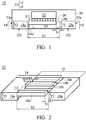
- FIG. 1 is a cross-sectional view of the package structure 10.
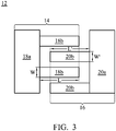
- FIG. 2 is a stereoscopic view of a leadframe of the package structure 10.
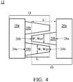
- FIG. 3 is a top view of a leadframe of the package structure 10.
- the package structure 10 includes a leadframe 12 including a first portion 14 and a second portion 16 opposite to the first portion 14.
- the first portion 14 includes a first base part 18a and a plurality of first extended parts 18b, for example two first extended parts 18b, connected to the first base part 18a.
- the second portion 16 includes a second base part 20a and a plurality of second extended parts 20b, for example two second extended parts 20b, connected to the second base part 20a.
- the number of extended parts may vary in the present invention, for example there may be three, four, or more, as long as there are at least two.
- the first extended parts 18b and the second extended parts 20b are arranged in such a way that they alternate with each other.
- a chip 22 is disposed on a part of the first extended parts 18b of the first portion 14 and the second extended parts 20b of the second portion 16 of the leadframe 12.
- the chip 22 includes power components, for example high-power components.
- the leadframe 12 is made of metal, such as copper or another appropriate metal material.
- the first portion 14 and the second portion 16 are comb-like structures.
- the first extended parts 18b of the first portion 14 extend towards the second base part 20a of the second portion 16.
- the second extended parts 20b of the second portion 16 extend towards the first base part 18a of the first portion 14.
- the first extended parts 18b of the first portion 14 and the second extended parts 20b of the second portion 16 are coplanar.
- first distance S1 between the first extended part 18b of the first portion 14 and the second base part 20a of the second portion 16.
- second distance S2 between the first base part 18a of the first portion 14 and the second base part 20a of the second portion 16.
- the second distance S2 is greater than or equal to about three times the first distance S1.
- the first distance S1 is in a range from about 100 ⁇ m to about 500 ⁇ m.
- first distance S1' between the second extended part 20b of the second portion 16 and the first base part 18a of the first portion 14.
- the second distance S2 is greater than or equal to about three times the first distance S1'.
- the first distance S1' is in a range from about 100 ⁇ m to about 500 ⁇ m.
- the first extended part 18b of the first portion 14 and the second extended part 20b of the second portion 16 have a first thickness T1.
- the first base part 18a of the first portion 14 and the second base part 20a of the second portion 16 have a second thickness T2.
- the second thickness T2 is greater than or equal to about two times the first thickness T1.
- the difference between the second thickness T2 and the first thickness T1 is greater than or equal to about 100 ⁇ m.
- the second thickness T2 is in a range from about 200 ⁇ m to about 400 ⁇ m.
- the first extended part 18b has a length L and a width W, and the length L is greater than or equal to about three times the width W.
- the second extended part 20b has a length L' and a width W', and the length L' is greater than or equal to about three times the width W'.
- the first extended part 18b and the second extended part 20b are in the shape of a rectangle.
- the first extended part 18b and the second extended part 20b being another appropriate shape, such as the shape of trapezoid, is also applicable in the present invention, as shown in FIG. 4 .
- the first extended part 18b of the first portion 14 has a bottom portion 24a connected to the first base part 18a and a top portion 24b towards the second base part 20a of the second portion 16.
- the first extended part 18b has a width W which decreases gradually from the bottom portion 24a to the top portion 24b of the first extended part 18b.
- the first extended part 18b of the first portion 14 has a length L and an average width Wav, and the length L is greater than or equal to about three times the average width Wav.
- the second extended part 20b of the second portion 16 has a bottom portion 26a connected to the second base part 20a and a top portion 26b towards the first base part 18a of the first portion 14.
- the second extended part 20b has a width W' which decreases gradually from the bottom portion 26a to the top portion 26b of the second extended part 20b.
- the second extended part 20b of the second portion 16 has a length L' and an average width Wav', and the length L' is greater than or equal to about three times the average width Wav'.
- the chip 22 is disposed on a part of the first extended parts 18b of the first portion 14 and the second extended parts 20b of the second portion 16 via solder balls 28.
- the solder balls 28 are first formed on the chip 22 by, for example electroplating.
- the reverse chip 22 is then attached on the first extended parts 18b of the first portion 14 and the second extended parts 20b of the second portion 16 by the solder balls 28 using the flip chip technology.
- a part of the first base part 18a of the first portion 14 further extends towards the second base part 20a of the second portion 16 to form an extending portion 18a' which is under a part of the first extended part 18b of the first portion 14.
- the third distance S3 is greater than or equal to about three times the first distance S1.
- the package structure 10 further includes an encapsulation material 30 covering the chip 22 and a part of the leadframe 12, exposing sidewalls 32a and bottoms 32b of the first base part 18a of the first portion 14 and the second base part 20a of the second portion 16 of the leadframe 12.
- FIG. 5 is a cross-sectional view of the package structure 10.
- FIG. 2 is a stereoscopic view of a leadframe of the package structure 10.
- FIG. 3 is a top view of a leadframe of the package structure 10.
- the package structure 10 includes a leadframe 12 including a first portion 14 and a second portion 16 opposite to the first portion 14.
- the first portion 14 includes a first base part 18a and a plurality of first extended parts 18b, for example two first extended parts 18b, connected to the first base part 18a.
- the second portion 16 includes a second base part 20a and a plurality of second extended parts 20b, for example two second extended parts 20b, connected to the second base part 20a.
- the number of extended parts may vary in the present invention, for example there may be three, four, or more, as long as there are at least two.
- the first extended parts 18b and the second extended parts 20b are arranged in such a way that they alternate with each other.
- a chip 22 is disposed on a part of the first extended parts 18b of the first portion 14 and the second extended parts 20b of the second portion 16 of the leadframe 12.
- the chip 22 includes power components, for example high-power components.
- the leadframe 12 is made of metal, such as copper or another appropriate metal material.
- the first portion 14 and the second portion 16 are comb-like structures.
- the first extended parts 18b of the first portion 14 extend towards the second base part 20a of the second portion 16.
- the second extended parts 20b of the second portion 16 extend towards the first base part 18a of the first portion 14.
- the first extended parts 18b of the first portion 14 and the second extended parts 20b of the second portion 16 are coplanar.
- first distance S1 between the first extended part 18b of the first portion 14 and the second base part 20a of the second portion 16.
- second distance S2 between the first base part 18a of the first portion 14 and the second base part 20a of the second portion 16.
- the second distance S2 is greater than or equal to about three times the first distance S1.
- the first distance S1 is in a range from about 100 ⁇ m to about 500 ⁇ m.
- first distance S1' between the second extended part 20b of the second portion 16 and the first base part 18a of the first portion 14.
- the second distance S2 is greater than or equal to about three times the first distance S1'.
- the first distance S1' is in a range from about 100 ⁇ m to about 500 ⁇ m.
- the first extended part 18b of the first portion 14 and the second extended part 20b of the second portion 16 have a first thickness T1.
- the first base part 18a of the first portion 14 and the second base part 20a of the second portion 16 have a second thickness T2.
- the second thickness T2 is greater than or equal to about two times the first thickness T1.
- the difference between the second thickness T2 and the first thickness T1 is greater than or equal to about 100 ⁇ m.
- the second thickness T2 is in a range from about 200 ⁇ m to about 400 ⁇ m.
- the first extended part 18b has a length L and a width W, and the length L is greater than or equal to about three times the width W.
- the second extended part 20b has a length L' and a width W', and the length L' is greater than or equal to about three times the width W'.
- the first extended part 18b and the second extended part 20b are in the shape of a rectangle.
- the first extended part 18b and the second extended part 20b being another appropriate shape, such as the shape of trapezoid, is also applicable in the present invention, as shown in FIG. 4 .
- the first extended part 18b of the first portion 14 has a bottom portion 24a connected to the first base part 18a and a top portion 24b towards the second base part 20a of the second portion 16.
- the first extended part 18b has a width W which decreases gradually from the bottom portion 24a to the top portion 24b of the first extended part 18b.
- the first extended part 18b of the first portion 14 has a length L and an average width Wav, and the length L is greater than or equal to about three times the average width Wav.
- the second extended part 20b of the second portion 16 has a bottom portion 26a connected to the second base part 20a and a top portion 26b towards the first base part 18a of the first portion 14.
- the second extended part 20b has a width W' which decreases gradually from the bottom portion 26a to the top portion 26b of the second extended part 20b.
- the second extended part 20b of the second portion 16 has a length L' and an average width Wav', and the length L' is greater than or equal to about three times the average width Wav'.
- the chip 22 is disposed on a part of the first extended parts 18b of the first portion 14 and the second extended parts 20b of the second portion 16 via copper pillars 34.
- the copper pillars 34 are first formed on the chip 22 by, for example electroplating.
- the reverse chip 22 is then attached on the first extended parts 18b of the first portion 14 and the second extended parts 20b of the second portion 16 by the copper pillars 34 using the flip chip technology.
- a part of the first base part 18a of the first portion 14 further extends towards the second base part 20a of the second portion 16 to form an extending portion 18a' which is under a part of the first extended part 18b of the first portion 14.
- the third distance S3 is greater than or equal to about three times the first distance S1.
- the package structure 10 further includes an encapsulation material 30 covering the chip 22 and a part of the leadframe 12, exposing sidewalls 32a and bottoms 32b of the first base part 18a of the first portion 14 and the second base part 20a of the second portion 16 of the leadframe 12.
- FIG. 6 is a cross-sectional view of the package structure 10.
- FIG. 2 is a stereoscopic view of a leadframe of the package structure 10.
- FIG. 3 is a top view of a leadframe of the package structure 10.
- the package structure 10 includes a leadframe 12 including a first portion 14 and a second portion 16 opposite to the first portion 14.
- the first portion 14 includes a first base part 18a and a plurality of first extended parts 18b, for example two first extended parts 18b, connected to the first base part 18a.
- the second portion 16 includes a second base part 20a and a plurality of second extended parts 20b, for example two second extended parts 20b, connected to the second base part 20a.
- the number of extended parts may vary in the present invention, for example there may be three, four, or more, as long as there are at least two.
- the first extended parts 18b and the second extended parts 20b are arranged in such a way that they alternate with each other.
- a chip 22 is disposed on a part of the first extended parts 18b of the first portion 14 and the second extended parts 20b of the second portion 16 of the leadframe 12.
- the chip 22 includes power components, for example high-power components.
- the leadframe 12 is made of metal, such as copper or another appropriate metal material.
- the first portion 14 and the second portion 16 are comb-like structures.
- the first extended parts 18b of the first portion 14 extend towards the second base part 20a of the second portion 16.
- the second extended parts 20b of the second portion 16 extend towards the first base part 18a of the first portion 14.
- the first extended parts 18b of the first portion 14 and the second extended parts 20b of the second portion 16 are coplanar.
- first distance S1 between the first extended part 18b of the first portion 14 and the second base part 20a of the second portion 16.
- second distance S2 between the first base part 18a of the first portion 14 and the second base part 20a of the second portion 16.
- the second distance S2 is greater than or equal to about three times the first distance S1.
- the first distance S1 is in a range from about 100 ⁇ m to about 500 ⁇ m.
- first distance S1' between the second extended part 20b of the second portion 16 and the first base part 18a of the first portion 14.
- the second distance S2 is greater than or equal to about three times the first distance S1'.
- the first distance S1' is in a range from about 100 ⁇ m to about 500 ⁇ m.
- the first extended part 18b of the first portion 14 and the second extended part 20b of the second portion 16 have a first thickness T1.
- the first base part 18a of the first portion 14 and the second base part 20a of the second portion 16 have a second thickness T2.
- the second thickness T2 is greater than or equal to about two times the first thickness T1.
- the difference between the second thickness T2 and the first thickness T1 is greater than or equal to about 100 ⁇ m.
- the second thickness T2 is in a range from about 200 ⁇ m to about 400 ⁇ m.
- the first extended part 18b has a length L and a width W, and the length L is greater than or equal to about three times the width W.
- the second extended part 20b has a length L' and a width W', and the length L' is greater than or equal to about three times the width W'.
- the first extended part 18b and the second extended part 20b are in the shape of a rectangle.
- the first extended part 18b and the second extended part 20b being another appropriate shape, such as the shape of trapezoid, is also applicable in the present invention, as shown in FIG. 4 .
- the first extended part 18b of the first portion 14 has a bottom portion 24a connected to the first base part 18a and a top portion 24b towards the second base part 20a of the second portion 16.
- the first extended part 18b has a width W which decreases gradually from the bottom portion 24a to the top portion 24b of the first extended part 18b.
- the first extended part 18b of the first portion 14 has a length L and an average width Wav, and the length L is greater than or equal to about three times the average width Wav.
- the second extended part 20b of the second portion 16 has a bottom portion 26a connected to the second base part 20a and a top portion 26b towards the first base part 18a of the first portion 14.
- the second extended part 20b has a width W' which decreases gradually from the bottom portion 26a to the top portion 26b of the second extended part 20b.
- the second extended part 20b of the second portion 16 has a length L' and an average width Wav', and the length L' is greater than or equal to about three times the average width Wav'.
- the chip 22 is disposed on a part of the first extended parts 18b of the first portion 14 and the second extended parts 20b of the second portion 16 via solder paste 36.
- the solder paste 36 is first formed on the first extended parts 18b of the first portion 14 and the second extended parts 20b of the second portion 16 by, for example screen printing.
- the reverse chip 22 is then attached on the first extended parts 18b of the first portion 14 and the second extended parts 20b of the second portion 16 by the solder paste 36 using the flip chip technology.
- other appropriate conductive materials such as silver paste, are also applicable in the present invention.
- a part of the first base part 18a of the first portion 14 further extends towards the second base part 20a of the second portion 16 to form an extending portion 18a' which is under a part of the first extended part 18b of the first portion 14.
- the third distance S3 is greater than or equal to about three times the first distance S1.
- the package structure 10 further includes an encapsulation material 30 covering the chip 22 and a part of the leadframe 12, exposing sidewalls 32a and bottoms 32b of the first base part 18a of the first portion 14 and the second base part 20a of the second portion 16 of the leadframe 12.
- a package structure with a specific comb-like leadframe is provided.
- Some appropriate dimensions and structure configurations of the leadframe are considered.
- the distance between the first base part and the second base part is greater than or equal to about three times the distance between the first extended part and the second base part, or the thickness of the base part is greater than or equal to about two times the thickness of the extended part, or the extended part has the shape of trapezoid.
- the insulation distance is insufficient.
- the distance between the first extended part and the second base part is greater than 500 ⁇ m, the size of the chip will exceed the range of the extended part, affecting the current conduction.
- the trapezoidal extended part improves the uniformity of the current conduction.
- current is collected along the chip, it is no longer conducted only through the metal structure in the chip, but is the "extended part" combined with the metal structure.
- the total cross-sectional area for current conduction is increased by disposing the chip on the extended parts protruding from the base part of the comb-like leadframe which further increases the carrying current.
- the increase of the cross-sectional area also reduces the resistance value simultaneously, so that when the current flows through it, the voltage difference generated is reduced, achieving uniform and stable current density and voltage during component operation.
Landscapes
- Lead Frames For Integrated Circuits (AREA)
- Physics & Mathematics (AREA)
- Geometry (AREA)
- Engineering & Computer Science (AREA)
- Microelectronics & Electronic Packaging (AREA)
Abstract
A package structure is provided. The package structure includes a leadframe including a first portion and a second portion. The first portion includes a first base part and a plurality of first extended parts connected to the first base part. The second portion includes a second base part and a plurality of second extended parts connected to the second base part. The first extended parts and the second extended parts are arranged in such a way that they alternate with each other. In the package structure, a chip is disposed on a part of the first extended parts of the first portion and the second extended parts of the second portion of the leadframe.
Description
- The invention relates to a package structure, and more particularly to a package structure with a comb-like leadframe.
- In a planar power component, a metal structure in the chip is required for collecting current, and then solder balls or wires lead the current to a leadframe or a substrate.
- However, the turn-on time can be put out of synchronization by the metal structure in the chip being too thin, by the current that can be carried being limited, and by there being a voltage difference on the metal structure.
- Therefore, development of a package structure capable of achieving uniform and stable current density and voltage during operation of the component is desirable.
- In accordance with one embodiment of the invention, a package structure is provided. The package structure includes a leadframe including a first portion and a second portion opposite to the first portion. The first portion includes a first base part and a plurality of first extended parts connected to the first base part. The second portion includes a second base part and a plurality of second extended parts connected to the second base part. The first extended parts and the second extended parts are arranged in such a way that they alternate with each other. In the package structure, a chip is disposed on a part of the first extended parts of the first portion and the second extended parts of the second portion of the leadframe.
- In some embodiments, the leadframe is made of metal. In some embodiments, the first portion and the second portion are comb-like structures. In some embodiments, the first extended parts of the first portion extend towards the second base part of the second portion, and the second extended parts of the second portion extend towards the first base part of the first portion. In some embodiments, the first extended parts of the first portion and the second extended parts of the second portion are coplanar.
- In some embodiments, there is a first distance between the first extended part of the first portion and the second base part of the second portion. In some embodiments, there is a second distance between the first base part of the first portion and the second base part of the second portion. In some embodiments, the second distance is greater than or equal to three times the first distance. In some embodiments, the first distance is in a range from 100µm to 500µm.
- In some embodiments, the first extended part of the first portion and the second extended part of the second portion have a first thickness. In some embodiments, the first base part of the first portion and the second base part of the second portion have a second thickness. In some embodiments, the second thickness is greater than or equal to two times the first thickness. In some embodiments, the difference between the second thickness and the first thickness is greater than or equal to 100µm. In some embodiments, the second thickness is in a range from 200µm to 400µm.
- In some embodiments, the first extended part of the first portion has a bottom portion connected to the first base part and a top portion towards the second base part of the second portion, and the first extended part has a width which decreases gradually from the bottom portion to the top portion of the first extended part. In some embodiments, the first extended part of the first portion has a length and an average width, and the length is greater than or equal to three times the average width.
- In some embodiments, the chip is disposed on a part of the first extended parts of the first portion and the second extended parts of the second portion via solder balls. In some embodiments, the chip is disposed on a part of the first extended parts of the first portion and the second extended parts of the second portion via copper pillars. In some embodiments, the chip is disposed on a part of the first extended parts of the first portion and the second extended parts of the second portion via solder paste, silver paste or a solder bar.
- In some embodiments, a part of the first base part of the first portion further extends towards the second base part of the second portion to a position which is under a part of the first extended part of the first portion. In some embodiments, there is a third distance between the first base part of the first portion and the second base part of the second portion. In some embodiments, the third distance is greater than or equal to three times the first distance.
- In some embodiments, the package structure further includes an encapsulation material covering the chip and a part of the leadframe, exposing sidewalls and bottoms of the first base part of the first portion and the second base part of the second portion of the leadframe.
- In the present invention, a package structure with a specific comb-like leadframe is provided. Some appropriate dimensions and structure configurations of the leadframe are considered. For example, the distance between the first base part and the second base part is greater than or equal to about three times the distance between the first extended part and the second base part, or the thickness of the base part is greater than or equal to about two times the thickness of the extended part, or the extended part has the shape of trapezoid. When the distance between the first extended part and the second base part is less than 100µm, the insulation distance is insufficient. When the distance between the first extended part and the second base part is greater than 500µm, the size of the chip will exceed the range of the extended part, affecting the current conduction. When the thickness of the extended part is too thick, there is a risk of exposing the extended parts from the encapsulation material. In addition, the trapezoidal extended part improves the uniformity of the current conduction. When current is collected along the chip, it is no longer conducted only through the metal structure in the chip, but is the "extended part" combined with the metal structure. The total cross-sectional area for current conduction is increased by disposing the chip on the extended parts protruding from the base part of the comb-like leadframe which further increases the carrying current. The increase of the cross-sectional area also reduces the resistance value simultaneously, so that when the current flows through it, the voltage difference generated is reduced, achieving uniform and stable current density and voltage during component operation.
- A detailed description is given in the following embodiments with reference to the accompanying drawings.
- The invention can be more fully understood by reading the subsequent detailed description and examples with references made to the accompanying drawings, wherein:
-
FIG. 1 is a cross-sectional view of a package structure in accordance with one embodiment of the invention; -
FIG. 2 is a stereoscopic view of a leadframe of a package structure in accordance with one embodiment of the invention; -
FIG. 3 is a top view of a leadframe of a package structure in accordance with one embodiment of the invention; -
FIG. 4 is a top view of a leadframe of a package structure in accordance with one embodiment of the invention; -
FIG. 5 is a cross-sectional view of a package structure in accordance with one embodiment of the invention; and -
FIG. 6 is a cross-sectional view of a package structure in accordance with one embodiment of the invention. - The following description is of the best-contemplated mode of carrying out the invention. This description is made for the purpose of illustrating the general principles of the invention and should not be taken in a limiting sense. The scope of the invention is determined by reference to the appended claims.
- In order to improve the uniformity and stability of current density and voltage of a power component during operation, the invention provides a package structure with a comb-like leadframe. The total cross-sectional area for current conduction can thus be increased by disposing a power component on extended parts protruding from a base part of the comb-like leadframe to achieve uniform and stable current density and voltage during component operation.
- Referring to
FIGS. 1, 2 and3 , in accordance with one embodiment of the invention, apackage structure 10 is provided.FIG. 1 is a cross-sectional view of thepackage structure 10.FIG. 2 is a stereoscopic view of a leadframe of thepackage structure 10.FIG. 3 is a top view of a leadframe of thepackage structure 10. - As shown in
FIGS. 1 and 2 , thepackage structure 10 includes aleadframe 12 including afirst portion 14 and asecond portion 16 opposite to thefirst portion 14. Thefirst portion 14 includes afirst base part 18a and a plurality of firstextended parts 18b, for example two firstextended parts 18b, connected to thefirst base part 18a. Thesecond portion 16 includes asecond base part 20a and a plurality of secondextended parts 20b, for example two secondextended parts 20b, connected to thesecond base part 20a. In accordance with various product requirements, the number of extended parts may vary in the present invention, for example there may be three, four, or more, as long as there are at least two. The firstextended parts 18b and the secondextended parts 20b are arranged in such a way that they alternate with each other. In thepackage structure 10, achip 22 is disposed on a part of the firstextended parts 18b of thefirst portion 14 and the secondextended parts 20b of thesecond portion 16 of theleadframe 12. In some embodiments, thechip 22 includes power components, for example high-power components. - In some embodiments, the
leadframe 12 is made of metal, such as copper or another appropriate metal material. InFIG. 2 , thefirst portion 14 and thesecond portion 16 are comb-like structures. The firstextended parts 18b of thefirst portion 14 extend towards thesecond base part 20a of thesecond portion 16. The secondextended parts 20b of thesecond portion 16 extend towards thefirst base part 18a of thefirst portion 14. The firstextended parts 18b of thefirst portion 14 and the secondextended parts 20b of thesecond portion 16 are coplanar. - In
FIG. 2 , there is a first distance S1 between the firstextended part 18b of thefirst portion 14 and thesecond base part 20a of thesecond portion 16. There is a second distance S2 between thefirst base part 18a of thefirst portion 14 and thesecond base part 20a of thesecond portion 16. In some embodiments, the second distance S2 is greater than or equal to about three times the first distance S1. In some embodiments, the first distance S1 is in a range from about 100µm to about 500µm. Similarly, there is a first distance S1' between the secondextended part 20b of thesecond portion 16 and thefirst base part 18a of thefirst portion 14. The second distance S2 is greater than or equal to about three times the first distance S1'. In some embodiments, the first distance S1' is in a range from about 100µm to about 500µm. - In
FIG. 2 , the firstextended part 18b of thefirst portion 14 and the secondextended part 20b of thesecond portion 16 have a first thickness T1. Thefirst base part 18a of thefirst portion 14 and thesecond base part 20a of thesecond portion 16 have a second thickness T2. In some embodiments, the second thickness T2 is greater than or equal to about two times the first thickness T1. In some embodiments, the difference between the second thickness T2 and the first thickness T1 is greater than or equal to about 100µm. In some embodiments, the second thickness T2 is in a range from about 200µm to about 400µm. - Referring to
FIG. 3 , the firstextended part 18b has a length L and a width W, and the length L is greater than or equal to about three times the width W. Similarly, the secondextended part 20b has a length L' and a width W', and the length L' is greater than or equal to about three times the width W'. InFIG. 3 , the firstextended part 18b and the secondextended part 20b are in the shape of a rectangle. - In some embodiments, the first
extended part 18b and the secondextended part 20b being another appropriate shape, such as the shape of trapezoid, is also applicable in the present invention, as shown inFIG. 4 . InFIG. 4 , the firstextended part 18b of thefirst portion 14 has abottom portion 24a connected to thefirst base part 18a and atop portion 24b towards thesecond base part 20a of thesecond portion 16. The firstextended part 18b has a width W which decreases gradually from thebottom portion 24a to thetop portion 24b of the firstextended part 18b. The firstextended part 18b of thefirst portion 14 has a length L and an average width Wav, and the length L is greater than or equal to about three times the average width Wav. Similarly, the secondextended part 20b of thesecond portion 16 has abottom portion 26a connected to thesecond base part 20a and atop portion 26b towards thefirst base part 18a of thefirst portion 14. The secondextended part 20b has a width W' which decreases gradually from thebottom portion 26a to thetop portion 26b of the secondextended part 20b. The secondextended part 20b of thesecond portion 16 has a length L' and an average width Wav', and the length L' is greater than or equal to about three times the average width Wav'. - In
FIG. 1 , thechip 22 is disposed on a part of the firstextended parts 18b of thefirst portion 14 and the secondextended parts 20b of thesecond portion 16 viasolder balls 28. InFIG. 1 , thesolder balls 28 are first formed on thechip 22 by, for example electroplating. Thereverse chip 22 is then attached on the firstextended parts 18b of thefirst portion 14 and the secondextended parts 20b of thesecond portion 16 by thesolder balls 28 using the flip chip technology. - In
FIG. 1 , in some embodiments, a part of thefirst base part 18a of thefirst portion 14 further extends towards thesecond base part 20a of thesecond portion 16 to form an extendingportion 18a' which is under a part of the firstextended part 18b of thefirst portion 14. InFIG. 1 , there is a third distance S3 between the extendingportion 18a' of thefirst base part 18a of thefirst portion 14 and thesecond base part 20a of thesecond portion 16. In some embodiments, the third distance S3 is greater than or equal to about three times the first distance S1. - In
FIG. 1 , thepackage structure 10 further includes anencapsulation material 30 covering thechip 22 and a part of theleadframe 12, exposingsidewalls 32a andbottoms 32b of thefirst base part 18a of thefirst portion 14 and thesecond base part 20a of thesecond portion 16 of theleadframe 12. - Referring to
FIGS. 5 ,2 and3 , in accordance with one embodiment of the invention, apackage structure 10 is provided.FIG. 5 is a cross-sectional view of thepackage structure 10.FIG. 2 is a stereoscopic view of a leadframe of thepackage structure 10.FIG. 3 is a top view of a leadframe of thepackage structure 10. - As shown in
FIGS. 5 and2 , thepackage structure 10 includes aleadframe 12 including afirst portion 14 and asecond portion 16 opposite to thefirst portion 14. Thefirst portion 14 includes afirst base part 18a and a plurality of firstextended parts 18b, for example two firstextended parts 18b, connected to thefirst base part 18a. Thesecond portion 16 includes asecond base part 20a and a plurality of secondextended parts 20b, for example two secondextended parts 20b, connected to thesecond base part 20a. In accordance with various product requirements, the number of extended parts may vary in the present invention, for example there may be three, four, or more, as long as there are at least two. The firstextended parts 18b and the secondextended parts 20b are arranged in such a way that they alternate with each other. In thepackage structure 10, achip 22 is disposed on a part of the firstextended parts 18b of thefirst portion 14 and the secondextended parts 20b of thesecond portion 16 of theleadframe 12. In some embodiments, thechip 22 includes power components, for example high-power components. - In some embodiments, the
leadframe 12 is made of metal, such as copper or another appropriate metal material. InFIG. 2 , thefirst portion 14 and thesecond portion 16 are comb-like structures. The firstextended parts 18b of thefirst portion 14 extend towards thesecond base part 20a of thesecond portion 16. The secondextended parts 20b of thesecond portion 16 extend towards thefirst base part 18a of thefirst portion 14. The firstextended parts 18b of thefirst portion 14 and the secondextended parts 20b of thesecond portion 16 are coplanar. - In
FIG. 2 , there is a first distance S1 between the firstextended part 18b of thefirst portion 14 and thesecond base part 20a of thesecond portion 16. There is a second distance S2 between thefirst base part 18a of thefirst portion 14 and thesecond base part 20a of thesecond portion 16. In some embodiments, the second distance S2 is greater than or equal to about three times the first distance S1. In some embodiments, the first distance S1 is in a range from about 100µm to about 500µm. Similarly, there is a first distance S1' between the secondextended part 20b of thesecond portion 16 and thefirst base part 18a of thefirst portion 14. The second distance S2 is greater than or equal to about three times the first distance S1'. In some embodiments, the first distance S1' is in a range from about 100µm to about 500µm. - In
FIG. 2 , the firstextended part 18b of thefirst portion 14 and the secondextended part 20b of thesecond portion 16 have a first thickness T1. Thefirst base part 18a of thefirst portion 14 and thesecond base part 20a of thesecond portion 16 have a second thickness T2. In some embodiments, the second thickness T2 is greater than or equal to about two times the first thickness T1. In some embodiments, the difference between the second thickness T2 and the first thickness T1 is greater than or equal to about 100µm. In some embodiments, the second thickness T2 is in a range from about 200µm to about 400µm. - Referring to
FIG. 3 , the firstextended part 18b has a length L and a width W, and the length L is greater than or equal to about three times the width W. Similarly, the secondextended part 20b has a length L' and a width W', and the length L' is greater than or equal to about three times the width W'. InFIG. 3 , the firstextended part 18b and the secondextended part 20b are in the shape of a rectangle. - In some embodiments, the first
extended part 18b and the secondextended part 20b being another appropriate shape, such as the shape of trapezoid, is also applicable in the present invention, as shown inFIG. 4 . InFIG. 4 , the firstextended part 18b of thefirst portion 14 has abottom portion 24a connected to thefirst base part 18a and atop portion 24b towards thesecond base part 20a of thesecond portion 16. The firstextended part 18b has a width W which decreases gradually from thebottom portion 24a to thetop portion 24b of the firstextended part 18b. The firstextended part 18b of thefirst portion 14 has a length L and an average width Wav, and the length L is greater than or equal to about three times the average width Wav. Similarly, the secondextended part 20b of thesecond portion 16 has abottom portion 26a connected to thesecond base part 20a and atop portion 26b towards thefirst base part 18a of thefirst portion 14. The secondextended part 20b has a width W' which decreases gradually from thebottom portion 26a to thetop portion 26b of the secondextended part 20b. The secondextended part 20b of thesecond portion 16 has a length L' and an average width Wav', and the length L' is greater than or equal to about three times the average width Wav'. - In
FIG. 5 , thechip 22 is disposed on a part of the firstextended parts 18b of thefirst portion 14 and the secondextended parts 20b of thesecond portion 16 viacopper pillars 34. InFIG. 5 , thecopper pillars 34 are first formed on thechip 22 by, for example electroplating. Thereverse chip 22 is then attached on the firstextended parts 18b of thefirst portion 14 and the secondextended parts 20b of thesecond portion 16 by thecopper pillars 34 using the flip chip technology. - In
FIG. 5 , in some embodiments, a part of thefirst base part 18a of thefirst portion 14 further extends towards thesecond base part 20a of thesecond portion 16 to form an extendingportion 18a' which is under a part of the firstextended part 18b of thefirst portion 14. InFIG. 5 , there is a third distance S3 between the extendingportion 18a' of thefirst base part 18a of thefirst portion 14 and thesecond base part 20a of thesecond portion 16. In some embodiments, the third distance S3 is greater than or equal to about three times the first distance S1. - In
FIG. 5 , thepackage structure 10 further includes anencapsulation material 30 covering thechip 22 and a part of theleadframe 12, exposingsidewalls 32a andbottoms 32b of thefirst base part 18a of thefirst portion 14 and thesecond base part 20a of thesecond portion 16 of theleadframe 12. - Referring to
FIGS. 6 ,2 and3 , in accordance with one embodiment of the invention, apackage structure 10 is provided.FIG. 6 is a cross-sectional view of thepackage structure 10.FIG. 2 is a stereoscopic view of a leadframe of thepackage structure 10.FIG. 3 is a top view of a leadframe of thepackage structure 10. - As shown in
FIGS. 6 and2 , thepackage structure 10 includes aleadframe 12 including afirst portion 14 and asecond portion 16 opposite to thefirst portion 14. Thefirst portion 14 includes afirst base part 18a and a plurality of firstextended parts 18b, for example two firstextended parts 18b, connected to thefirst base part 18a. Thesecond portion 16 includes asecond base part 20a and a plurality of secondextended parts 20b, for example two secondextended parts 20b, connected to thesecond base part 20a. In accordance with various product requirements, the number of extended parts may vary in the present invention, for example there may be three, four, or more, as long as there are at least two. The firstextended parts 18b and the secondextended parts 20b are arranged in such a way that they alternate with each other. In thepackage structure 10, achip 22 is disposed on a part of the firstextended parts 18b of thefirst portion 14 and the secondextended parts 20b of thesecond portion 16 of theleadframe 12. In some embodiments, thechip 22 includes power components, for example high-power components. - In some embodiments, the
leadframe 12 is made of metal, such as copper or another appropriate metal material. InFIG. 2 , thefirst portion 14 and thesecond portion 16 are comb-like structures. The firstextended parts 18b of thefirst portion 14 extend towards thesecond base part 20a of thesecond portion 16. The secondextended parts 20b of thesecond portion 16 extend towards thefirst base part 18a of thefirst portion 14. The firstextended parts 18b of thefirst portion 14 and the secondextended parts 20b of thesecond portion 16 are coplanar. - In
FIG. 2 , there is a first distance S1 between the firstextended part 18b of thefirst portion 14 and thesecond base part 20a of thesecond portion 16. There is a second distance S2 between thefirst base part 18a of thefirst portion 14 and thesecond base part 20a of thesecond portion 16. In some embodiments, the second distance S2 is greater than or equal to about three times the first distance S1. In some embodiments, the first distance S1 is in a range from about 100µm to about 500µm. Similarly, there is a first distance S1' between the secondextended part 20b of thesecond portion 16 and thefirst base part 18a of thefirst portion 14. The second distance S2 is greater than or equal to about three times the first distance S1'. In some embodiments, the first distance S1' is in a range from about 100µm to about 500µm. - In
FIG. 2 , the firstextended part 18b of thefirst portion 14 and the secondextended part 20b of thesecond portion 16 have a first thickness T1. Thefirst base part 18a of thefirst portion 14 and thesecond base part 20a of thesecond portion 16 have a second thickness T2. In some embodiments, the second thickness T2 is greater than or equal to about two times the first thickness T1. In some embodiments, the difference between the second thickness T2 and the first thickness T1 is greater than or equal to about 100µm. In some embodiments, the second thickness T2 is in a range from about 200µm to about 400µm. - Referring to
FIG. 3 , the firstextended part 18b has a length L and a width W, and the length L is greater than or equal to about three times the width W. Similarly, the secondextended part 20b has a length L' and a width W', and the length L' is greater than or equal to about three times the width W'. InFIG. 3 , the firstextended part 18b and the secondextended part 20b are in the shape of a rectangle. - In some embodiments, the first
extended part 18b and the secondextended part 20b being another appropriate shape, such as the shape of trapezoid, is also applicable in the present invention, as shown inFIG. 4 . InFIG. 4 , the firstextended part 18b of thefirst portion 14 has abottom portion 24a connected to thefirst base part 18a and atop portion 24b towards thesecond base part 20a of thesecond portion 16. The firstextended part 18b has a width W which decreases gradually from thebottom portion 24a to thetop portion 24b of the firstextended part 18b. The firstextended part 18b of thefirst portion 14 has a length L and an average width Wav, and the length L is greater than or equal to about three times the average width Wav. Similarly, the secondextended part 20b of thesecond portion 16 has abottom portion 26a connected to thesecond base part 20a and atop portion 26b towards thefirst base part 18a of thefirst portion 14. The secondextended part 20b has a width W' which decreases gradually from thebottom portion 26a to thetop portion 26b of the secondextended part 20b. The secondextended part 20b of thesecond portion 16 has a length L' and an average width Wav', and the length L' is greater than or equal to about three times the average width Wav'. - In
FIG. 6 , thechip 22 is disposed on a part of the firstextended parts 18b of thefirst portion 14 and the secondextended parts 20b of thesecond portion 16 viasolder paste 36. InFIG. 6 , thesolder paste 36 is first formed on the firstextended parts 18b of thefirst portion 14 and the secondextended parts 20b of thesecond portion 16 by, for example screen printing. Thereverse chip 22 is then attached on the firstextended parts 18b of thefirst portion 14 and the secondextended parts 20b of thesecond portion 16 by thesolder paste 36 using the flip chip technology. In some embodiments, other appropriate conductive materials, such as silver paste, are also applicable in the present invention. - In
FIG. 6 , in some embodiments, a part of thefirst base part 18a of thefirst portion 14 further extends towards thesecond base part 20a of thesecond portion 16 to form an extendingportion 18a' which is under a part of the firstextended part 18b of thefirst portion 14. InFIG. 6 , there is a third distance S3 between the extendingportion 18a' of thefirst base part 18a of thefirst portion 14 and thesecond base part 20a of thesecond portion 16. In some embodiments, the third distance S3 is greater than or equal to about three times the first distance S1. - In
FIG. 6 , thepackage structure 10 further includes anencapsulation material 30 covering thechip 22 and a part of theleadframe 12, exposingsidewalls 32a andbottoms 32b of thefirst base part 18a of thefirst portion 14 and thesecond base part 20a of thesecond portion 16 of theleadframe 12. - In the present invention, a package structure with a specific comb-like leadframe is provided. Some appropriate dimensions and structure configurations of the leadframe are considered. For example, the distance between the first base part and the second base part is greater than or equal to about three times the distance between the first extended part and the second base part, or the thickness of the base part is greater than or equal to about two times the thickness of the extended part, or the extended part has the shape of trapezoid. When the distance between the first extended part and the second base part is less than 100µm, the insulation distance is insufficient. When the distance between the first extended part and the second base part is greater than 500µm, the size of the chip will exceed the range of the extended part, affecting the current conduction. When the thickness of the extended part is too thick, there is a risk of exposing the extended parts from the encapsulation material. In addition, the trapezoidal extended part improves the uniformity of the current conduction. When current is collected along the chip, it is no longer conducted only through the metal structure in the chip, but is the "extended part" combined with the metal structure. The total cross-sectional area for current conduction is increased by disposing the chip on the extended parts protruding from the base part of the comb-like leadframe which further increases the carrying current. The increase of the cross-sectional area also reduces the resistance value simultaneously, so that when the current flows through it, the voltage difference generated is reduced, achieving uniform and stable current density and voltage during component operation.
- While the invention has been described by way of example and in terms of embodiment, it is to be understood that the invention is not limited thereto. On the contrary, it is intended to cover various modifications and similar arrangements (as would be apparent to those skilled in the art). Therefore, the scope of the appended claims should be accorded the broadest interpretation so as to encompass all such modifications and similar arrangements.
Claims (15)
- A package structure (10), comprising:a leadframe (12) comprising a first portion (14) and a second portion (16) opposite to the first portion (14), wherein the first portion (14) comprises a first base part (18a) and a plurality of first extended parts (18b) connected to the first base part (18a), the second portion (16) comprises a second base part (20a) and a plurality of second extended parts (20b) connected to the second base part (20a), and the first extended parts (18b) and the second extended parts (20b) are arranged in such a way that they alternate with each other; anda chip (22) disposed on a part of the first extended parts (18b) of the first portion (14) and the second extended parts (20b) of the second portion (16) of the leadframe (12).
- The package structure as claimed in claim 1, wherein the first portion (14) and the second portion (16) are comb-like structures.
- The package structure as claimed in claim 2, wherein the first extended parts (18b) of the first portion (14) extend towards the second base part (20a) of the second portion (16), and the second extended parts (20b) of the second portion (16) extend towards the first base part (18a) of the first portion (14).
- The package structure as claimed in claim 3, wherein the first extended parts (18b) of the first portion (14) and the second extended parts (20b) of the second portion (16) are coplanar.
- The package structure as claimed in claim 4, wherein there is a first distance (S1) between the first extended part (18b) of the first portion (14) and the second base part (20a) of the second portion (16).
- The package structure as claimed in claim 5, wherein there is a second distance (S2) between the first base part (18a) of the first portion (14) and the second base part (20a) of the second portion (16).
- The package structure as claimed in claim 6, wherein the second distance (S2) is greater than or equal to three times the first distance (S1).
- The package structure as claimed in any of the claims 5 to 7, wherein the first distance (S1) is in a range from 100µm to 500µm.
- The package structure as claimed in any of the claims 1 to 8, wherein the first extended part (18b) of the first portion (14) and the second extended part (20b) of the second portion (16) have a first thickness (T1).
- The package structure as claimed in claim 9, wherein the first base part (18a) of the first portion (14) and the second base part (20a) of the second portion (16) have a second thickness (T2).
- The package structure as claimed in claim 10, wherein the second thickness (T2) is greater than or equal to two times the first thickness (T1).
- The package structure as claimed in any of the claims 1 to 11, wherein the first extended part (18b) of the first portion (14) has a bottom portion (24a) connected to the first base part (18a) and a top portion (24b) towards the second base part (20a) of the second portion (16), and the first extended part (18b) has a width (W) which decreases gradually from the bottom portion (24a) to the top portion (24b) of the first extended part (18b).
- The package structure as claimed in any of the claims 5 to 12, wherein a part of the first base part (18a) of the first portion (14) further extends towards the second base part (20a) of the second portion (16) to a position which is under a part of the first extended part (18b) of the first portion (14).
- The package structure as claimed in claim 13, wherein there is a third distance (S3) between the first base part (18a) of the first portion (14) and the second base part (20a) of the second portion (16).
- The package structure as claimed in any of the claims 1 to 14, further comprising an encapsulation material (30) covering the chip (22) and a part of the leadframe (12), exposing sidewalls (32a) and bottoms (32b) of the first base part (18a) of the first portion (14) and the second base part (20a) of the second portion (16) of the leadframe (12).
Applications Claiming Priority (1)
| Application Number | Priority Date | Filing Date | Title |
|---|---|---|---|
| US16/786,139 US20210249339A1 (en) | 2020-02-10 | 2020-02-10 | Package structures |
Publications (1)
| Publication Number | Publication Date |
|---|---|
| EP3863048A1 true EP3863048A1 (en) | 2021-08-11 |
Family
ID=69784066
Family Applications (1)
| Application Number | Title | Priority Date | Filing Date |
|---|---|---|---|
| EP20159326.6A Withdrawn EP3863048A1 (en) | 2020-02-10 | 2020-02-25 | Package structures |
Country Status (4)
| Country | Link |
|---|---|
| US (1) | US20210249339A1 (en) |
| EP (1) | EP3863048A1 (en) |
| CN (1) | CN113257769A (en) |
| TW (1) | TW202131464A (en) |
Families Citing this family (1)
| Publication number | Priority date | Publication date | Assignee | Title |
|---|---|---|---|---|
| US12519043B2 (en) * | 2022-02-10 | 2026-01-06 | Advanced Semiconductor Engineering, Inc. | Electronic package including leadframe for power transmission |
Citations (3)
| Publication number | Priority date | Publication date | Assignee | Title |
|---|---|---|---|---|
| US20080035959A1 (en) * | 2006-08-09 | 2008-02-14 | Jiang Hunt H | Chip scale package for power devices and method for making the same |
| US20080048218A1 (en) * | 2006-08-24 | 2008-02-28 | Jiang Hunt H | Method and flip chip structure for power devices |
| US20160247748A1 (en) * | 2015-02-24 | 2016-08-25 | Navitas Semiconductor Inc. | Electronic packages for flip chip devices |
Family Cites Families (12)
| Publication number | Priority date | Publication date | Assignee | Title |
|---|---|---|---|---|
| IN171404B (en) * | 1986-08-27 | 1992-10-03 | Digital Equipment Corp | |
| US5016082A (en) * | 1988-09-16 | 1991-05-14 | Delco Electronics Corporation | Integrated circuit interconnect design |
| JPH08102517A (en) * | 1994-09-30 | 1996-04-16 | Nec Corp | Semiconductor device and lead frame |
| JP3527350B2 (en) * | 1996-02-01 | 2004-05-17 | 株式会社ルネサステクノロジ | Semiconductor device |
| US20090045491A1 (en) * | 2007-08-15 | 2009-02-19 | Advanced Semiconductor Engineering, Inc. | Semiconductor package structure and leadframe thereof |
| CN101562163B (en) * | 2008-04-17 | 2011-06-01 | 力成科技股份有限公司 | Semiconductor package structure based on lead frame and its applicable lead frame |
| US20100164078A1 (en) * | 2008-12-31 | 2010-07-01 | Ruben Madrid | Package assembly for semiconductor devices |
| CN102779803A (en) * | 2011-05-10 | 2012-11-14 | 立锜科技股份有限公司 | Integrated circuit chip package and method of manufacturing the same |
| CN202259248U (en) * | 2011-08-30 | 2012-05-30 | 神锜科技股份有限公司 | Packaging structure, small-outline packaging structure and electronic chip thereof |
| CN103390572A (en) * | 2012-05-11 | 2013-11-13 | 苏州贝斯特石英有限公司 | Quartz boat |
| CN104900622B (en) * | 2014-03-06 | 2018-02-06 | 扬智科技股份有限公司 | Lead frame and chip package structure |
| CN108878394B (en) * | 2018-07-27 | 2024-08-16 | 杭州士兰微电子股份有限公司 | Power packaging structure and lead frame thereof |
-
2020
- 2020-02-10 US US16/786,139 patent/US20210249339A1/en not_active Abandoned
- 2020-02-25 EP EP20159326.6A patent/EP3863048A1/en not_active Withdrawn
- 2020-07-10 TW TW109123283A patent/TW202131464A/en unknown
- 2020-07-10 CN CN202010662696.XA patent/CN113257769A/en active Pending
Patent Citations (3)
| Publication number | Priority date | Publication date | Assignee | Title |
|---|---|---|---|---|
| US20080035959A1 (en) * | 2006-08-09 | 2008-02-14 | Jiang Hunt H | Chip scale package for power devices and method for making the same |
| US20080048218A1 (en) * | 2006-08-24 | 2008-02-28 | Jiang Hunt H | Method and flip chip structure for power devices |
| US20160247748A1 (en) * | 2015-02-24 | 2016-08-25 | Navitas Semiconductor Inc. | Electronic packages for flip chip devices |
Also Published As
| Publication number | Publication date |
|---|---|
| TW202131464A (en) | 2021-08-16 |
| US20210249339A1 (en) | 2021-08-12 |
| CN113257769A (en) | 2021-08-13 |
Similar Documents
| Publication | Publication Date | Title |
|---|---|---|
| KR101926854B1 (en) | Semiconductor device | |
| US9520345B2 (en) | Semiconductor module, semiconductor device having semiconductor module, and method of manufacturing semiconductor module | |
| US5343074A (en) | Semiconductor device having voltage distribution ring(s) and method for making the same | |
| US3763403A (en) | Isolated heat-sink semiconductor device | |
| US20190157403A1 (en) | Semiconductor device, semiconductor module, and packaged semiconductor device | |
| EP1107311B1 (en) | Semiconductor die package including cup-shaped leadframe | |
| US10944046B2 (en) | Semiconductor device | |
| US20090020859A1 (en) | Quad flat package with exposed common electrode bars | |
| US9299644B1 (en) | Integrated circuit packaging system with routed circuit lead array and method of manufacture thereof | |
| US10490659B2 (en) | Semiconductor device and portable apparatus using the same | |
| US7233064B2 (en) | Semiconductor BGA package having a segmented voltage plane and method of making | |
| EP1137065A2 (en) | Semiconductor device and manufacturing method thereof | |
| US20210249339A1 (en) | Package structures | |
| US11315857B2 (en) | Package structures | |
| CN102054717A (en) | Semiconductor chip grid array package and manufacturing method thereof | |
| CN106340496B (en) | Chip package structure and manufacturing method thereof | |
| CN206834165U (en) | A kind of TO cermets shell structure | |
| US7429785B2 (en) | Stacked integrated circuit chip assembly | |
| EP2722885B1 (en) | Surface mountable power components | |
| KR20190085587A (en) | High thermal conductivity semiconductor package | |
| EP4372809A1 (en) | Silicon carbide diode mounted on a leadframe by diffusion soldering using a copper/nickel/tin metallisation stack | |
| US7579675B2 (en) | Semiconductor device having surface mountable external contact areas and method for producing the same | |
| EP4654260A1 (en) | Semiconductor device | |
| JP3676163B2 (en) | Mounting structure of bare chip of switching element | |
| US20210287964A1 (en) | Semiconductor devices including parallel electrically conductive layers |
Legal Events
| Date | Code | Title | Description |
|---|---|---|---|
| PUAI | Public reference made under article 153(3) epc to a published international application that has entered the european phase |
Free format text: ORIGINAL CODE: 0009012 |
|
| STAA | Information on the status of an ep patent application or granted ep patent |
Free format text: STATUS: THE APPLICATION HAS BEEN PUBLISHED |
|
| AK | Designated contracting states |
Kind code of ref document: A1 Designated state(s): AL AT BE BG CH CY CZ DE DK EE ES FI FR GB GR HR HU IE IS IT LI LT LU LV MC MK MT NL NO PL PT RO RS SE SI SK SM TR |
|
| STAA | Information on the status of an ep patent application or granted ep patent |
Free format text: STATUS: THE APPLICATION IS DEEMED TO BE WITHDRAWN |
|
| 18D | Application deemed to be withdrawn |
Effective date: 20220212 |