EP3863014A1 - Rechnergesteuerte speicherzelle und verarbeitungsanordnungsvorrichtung mit verhältnislosem schreibport - Google Patents
Rechnergesteuerte speicherzelle und verarbeitungsanordnungsvorrichtung mit verhältnislosem schreibport Download PDFInfo
- Publication number
- EP3863014A1 EP3863014A1 EP21155509.9A EP21155509A EP3863014A1 EP 3863014 A1 EP3863014 A1 EP 3863014A1 EP 21155509 A EP21155509 A EP 21155509A EP 3863014 A1 EP3863014 A1 EP 3863014A1
- Authority
- EP
- European Patent Office
- Prior art keywords
- write
- bit line
- cell
- read
- storage
- Prior art date
- Legal status (The legal status is an assumption and is not a legal conclusion. Google has not performed a legal analysis and makes no representation as to the accuracy of the status listed.)
- Granted
Links
Images


Classifications
-
- G—PHYSICS
- G11—INFORMATION STORAGE
- G11C—STATIC STORES
- G11C11/00—Digital stores characterised by the use of particular electric or magnetic storage elements; Storage elements therefor
- G11C11/21—Digital stores characterised by the use of particular electric or magnetic storage elements; Storage elements therefor using electric elements
- G11C11/34—Digital stores characterised by the use of particular electric or magnetic storage elements; Storage elements therefor using electric elements using semiconductor devices
- G11C11/40—Digital stores characterised by the use of particular electric or magnetic storage elements; Storage elements therefor using electric elements using semiconductor devices using transistors
- G11C11/41—Digital stores characterised by the use of particular electric or magnetic storage elements; Storage elements therefor using electric elements using semiconductor devices using transistors forming static cells with positive feedback, i.e. cells not needing refreshing or charge regeneration, e.g. bistable multivibrator or Schmitt trigger
- G11C11/412—Digital stores characterised by the use of particular electric or magnetic storage elements; Storage elements therefor using electric elements using semiconductor devices using transistors forming static cells with positive feedback, i.e. cells not needing refreshing or charge regeneration, e.g. bistable multivibrator or Schmitt trigger using field-effect transistors only
-
- G—PHYSICS
- G11—INFORMATION STORAGE
- G11C—STATIC STORES
- G11C11/00—Digital stores characterised by the use of particular electric or magnetic storage elements; Storage elements therefor
- G11C11/21—Digital stores characterised by the use of particular electric or magnetic storage elements; Storage elements therefor using electric elements
- G11C11/34—Digital stores characterised by the use of particular electric or magnetic storage elements; Storage elements therefor using electric elements using semiconductor devices
- G11C11/40—Digital stores characterised by the use of particular electric or magnetic storage elements; Storage elements therefor using electric elements using semiconductor devices using transistors
- G11C11/41—Digital stores characterised by the use of particular electric or magnetic storage elements; Storage elements therefor using electric elements using semiconductor devices using transistors forming static cells with positive feedback, i.e. cells not needing refreshing or charge regeneration, e.g. bistable multivibrator or Schmitt trigger
- G11C11/413—Auxiliary circuits, e.g. for addressing, decoding, driving, writing, sensing, timing or power reduction
- G11C11/417—Auxiliary circuits, e.g. for addressing, decoding, driving, writing, sensing, timing or power reduction for memory cells of the field-effect type
- G11C11/419—Read-write [R-W] circuits
-
- G—PHYSICS
- G06—COMPUTING OR CALCULATING; COUNTING
- G06F—ELECTRIC DIGITAL DATA PROCESSING
- G06F15/00—Digital computers in general; Data processing equipment in general
- G06F15/76—Architectures of general purpose stored program computers
- G06F15/78—Architectures of general purpose stored program computers comprising a single central processing unit
- G06F15/7839—Architectures of general purpose stored program computers comprising a single central processing unit with memory
-
- G—PHYSICS
- G11—INFORMATION STORAGE
- G11C—STATIC STORES
- G11C11/00—Digital stores characterised by the use of particular electric or magnetic storage elements; Storage elements therefor
- G11C11/21—Digital stores characterised by the use of particular electric or magnetic storage elements; Storage elements therefor using electric elements
- G11C11/34—Digital stores characterised by the use of particular electric or magnetic storage elements; Storage elements therefor using electric elements using semiconductor devices
- G11C11/40—Digital stores characterised by the use of particular electric or magnetic storage elements; Storage elements therefor using electric elements using semiconductor devices using transistors
- G11C11/41—Digital stores characterised by the use of particular electric or magnetic storage elements; Storage elements therefor using electric elements using semiconductor devices using transistors forming static cells with positive feedback, i.e. cells not needing refreshing or charge regeneration, e.g. bistable multivibrator or Schmitt trigger
- G11C11/413—Auxiliary circuits, e.g. for addressing, decoding, driving, writing, sensing, timing or power reduction
- G11C11/417—Auxiliary circuits, e.g. for addressing, decoding, driving, writing, sensing, timing or power reduction for memory cells of the field-effect type
- G11C11/418—Address circuits
-
- G—PHYSICS
- G11—INFORMATION STORAGE
- G11C—STATIC STORES
- G11C7/00—Arrangements for writing information into, or reading information out from, a digital store
- G11C7/10—Input/output [I/O] data interface arrangements, e.g. I/O data control circuits, I/O data buffers
- G11C7/1006—Data managing, e.g. manipulating data before writing or reading out, data bus switches or control circuits therefor
-
- G—PHYSICS
- G11—INFORMATION STORAGE
- G11C—STATIC STORES
- G11C8/00—Arrangements for selecting an address in a digital store
- G11C8/16—Multiple access memory array, e.g. addressing one storage element via at least two independent addressing line groups
Definitions
- the disclosure relates generally to a static random access memory cell that may be used for computations.
- An array of memory cells such as dynamic random access memory (DRAM) cells, static random access memory (SRAM) cells, content addressable memory (CAM) cells or non-volatile memory cells, is a well-known mechanism used in various computer or processor based devices to store digital bits of data.
- the various computer and processor based devices may include computer systems, smartphone devices, consumer electronic products, televisions, internet switches and routers and the like.
- the array of memory cells are typically packaged in an integrated circuit or may be packaged within an integrated circuit that also has a processing device within the integrated circuit.
- the different types of typical memory cells have different capabilities and characteristics that distinguish each type of memory cell. For example, DRAM cells take longer to access, lose their data contents unless periodically refreshed, but are relatively cheap to manufacture due to the simple structure of each DRAM cell.
- SRAM cells have faster access times, do not lose their data content unless power is removed from the SRAM cell and are relatively more expensive since each SRAM cell is more complicated than a DRAM cell.
- CAM cells have a unique function of being able to address content easily within the cells and are more expensive to manufacture since each CAM cell requires more circuitry to achieve the content addressing functionality.
- the computation devices may include a microprocessor, a CPU, a microcontroller and the like. These computation devices are typically manufactured on an integrated circuit, but may also be manufactured on an integrated circuit that also has some amount of memory integrated onto the integrated circuit. In these known integrated circuits with a computation device and memory, the computation device performs the computation of the digital binary data bits while the memory is used to store various digital binary data including, for example, the instructions being executed by the computation device and the data being operated on by the computation device.
- a processor array to perform computations may be formed from memory cells. These devices may be known as in-memory computational devices.
- Big data operations are data processing operations in which a large amount of data must be processed.
- Machine learning uses artificial intelligence algorithms to analyze data and typically require a lot of data to perform.
- the big data operations and machine learning also are typically very computationally intensive applications that often encounter input/output issues due to a bandwidth bottleneck between the computational device and the memory that stores the data.
- the above in-memory computational devices may be used, for example, for these big data operations and machine learning applications since the in-memory computational devices perform the computations within the memory thereby eliminating the bandwidth bottleneck.
- An SRAM cell can be configured to perform Boolean operations such as AND, OR, NAND and NOR, Exclusive OR and NOR. This SRAM cell can also support a Selective Write operation.
- the typical SRAM cell requires stronger writing transistors than the transistors in the storage latch to over write the storage data.
- a ratio of the transistor strengths of the write transistor and the storage transistor may be known as a write ratio.
- the write ratio is 2 to 3 meaning that the writing transistor is 2 to 3 times of the strength of the storage transistor for the writing to be successful.
- a computational memory cell that may be an SRAM cell, with a write port to perform Boolean operations such as AND, OR, NAND, NOR, XOR (Exclusive OR) and XNOR (Exclusive NOR) that is able to do the writing ratioless.
- a computational memory cell and processing array have a ratioless write port so that a write to the memory cell does not need to overcome the drive strength of a PMOS transistor that is part of the storage cell of the memory cell.
- the computational memory cell also may have a second read port that has an isolation circuit.
- the disclosure is particularly applicable to a CMOS implemented memory cell and processing array with a plurality of the memory cells that are capable to performing logic functions with a ratioless write port and it is in this context that the disclosure will be described. It will be appreciated, however, that the memory cell and processing array has greater utility and is not limited to the below disclosed implementations since the memory cell may be constructed using different processes and may have different circuit configurations than those disclosed below that perform the logic function and so are within the scope of this disclosure.
- a dual port SRAM and 3-port cells are disclosed below and in the figures.
- the SRAM computation cell and processing array may also be implemented with an SRAM cell having more ports and the disclosure is not limited to the SRAM cells disclosed below. It is also understood that the SRAM cells having more ports may be slightly differently constructed than the SRAM cells shown in the figures, but one skilled in the art would understand how to construct those SRAMs with more ports from the disclosure below.
- SRAM cell for computation and the processing array using the memory cells may be implemented using various different types of memory cells including DRAMs, CAMs, non-volatile memory cells and non-volatile memory devices and these implementations using the various types of memory cells are within the scope of the disclosure.
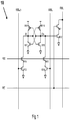
- FIG 1 illustrates a dual port SRAM cell 10 that may be used for computation.
- the dual port SRAM cell may include two cross coupled inverters (transistors M17, M19 pair as one inverter and transistors M18 and M110 pair as another inverter) that form a latch or storage cell and access transistors M11-M16 that are coupled together as shown in Figure 1 to form an SRAM cell.
- the SRAM cell may be operated as a storage latch and may have a read port and a write port so that the SRAM cell is a dual port SRAM cell.
- the two inverters are cross coupled since the input of the first inverter is connected to the output of the second inverter and the output of the first inverter is coupled to the input of the second inverter as shown in Figure 1 .
- a Write Word line carries a signal and is called WE (see Figure 1 ) and a write bit line and its complement are called WBL and WBLb, respectively.
- the Write word line (WE) is coupled to the gate of each of the two access transistors M15, M16 that are part of the SRAM cell.
- the write bit line and its complement (WBL and WBLb) are each coupled to a gate of the respective access transistors M13, M14 as shown in Figure 1 and M13 is coupled to M15 and M14 is coupled to M16.
- the source of each of transistors M13 and M14 is coupled to ground.
- the drain of each of those access transistors M15, M16 is coupled to each side of the cross coupled inverters (labeled D and Db in Figure 1 ).
- the circuit in Figure 1 may also have a read word line RE, a read bit line RBL and a read port formed by transistors M11, M12 coupled together to form an isolation circuit.
- the read word line RE may be coupled to the gate of transistor M11 that forms part of the read port while the read bit line is coupled to the drain terminal of transistor M11.
- the gate of transistor M12 may be coupled to the Db output from the cross coupled inverters and the source of transistor M12 may be coupled to ground.
- the dual port SRAM cell may read data stored in the latch using a signal on the read word line (RE) to address/activate the dual port SRAM cell and the read bit line (RBL) to read the data stored in the dual port SRAM cell.
- the dual port SRAM cell may write data into the dual port SRAM cell by addressing/activating the dual port SRAM cell using a signal on the write word line (WE) and then writing data into the dual port SRAM cell using the write bit lines (WBL, WBLb).
- multiple cells can be turned on to perform an AND function between the data stored in the cells that were turned on.
- a number of cells in a column of the processing array 20 in Figure 2 such as cell 00,..., cell m0, may be activated by the RE signal for each of those cells.
- RBL is pre-charged high and if the Db signal of all cells that are turned on by RE are "0", then RBL stays high.
- the gate of transistor M11 is turned on by the RE signal, the gate of M12 is not turned on since the Db signal is low.
- the RBL line is not connected to the ground to which the source of transistor M12 is connected and the RBL line is not discharged.
- the write operation is activated by WE and the data is written by toggling of WBL and WBLb.
- the read operation is activated by RE and the read data is accessed on RBL.
- the Db signal of the cell 10 may be coupled to a gate of transistor M12 to drive the RBL line.
- the Db signal is isolated from the RBL line and its signal/voltage level by the transistors M11, M12 (together forming the isolation circuit). Because the Db signal/value is isolated from the RBL line and signal/voltage level, the Db signal is not susceptible to the lower bit line level caused by multiple "0" data stored in multiple cells. Therefore, for the cell in Figure 1 , there is no limitation of how many cells can be turned on to drive RBL.
- the cell offers more operands for the Boolean functions such as AND function described above and NOR/OR/NAND/XOR/XNOR functions described in co-pending and commonly owned 15/709,401 filed September 19, 2017 (now issued as US Patent 10,249,362 on April 2, 2019 ) and 15/709,399 filed September 19, 2017 and U.S. Provisional Application No. 62/430,767 filed December 6, 2016 (incorporated herein by reference) since there is no limit of how many cells can be turned on to drive RBL.
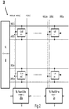
- FIG 2 illustrates a processing array device 20 that may incorporate the dual port SRAM cell of Figure 1 , in which each cell, such as cell 00, ..., cell 0n and cell m0, ...., cell mn, is the cell shown in Figure 1 .
- the cells form an array of cells laid out as shown in Figure 2 .
- the processing array 20 may perform computations using the computational capabilities of the dual port SRAM cell described above.
- the array device 20 may be formed by M word lines (such as RE0, WE0,...., REm, WEm) and N bit lines (such as WBL0, WBLb0, RBL0, ...., WBLn, WBLbn, RBLn.)
- the array device 20 may also include a word line generator 24 (WL Generator) that generates word line signals as well as a plurality of bit line read/write logic 26 (such as BL Read/Write Logic 0,...., BL Read/Write Logic n) that perform read and write operations using the bit lines.
- the array device 20 may be manufactured on an integrated circuit or may be integrated into another integrated circuit depending on the use of the processing array 20.
- the word line generator 24 may generate one or multiple RE signals in a cycle to turn on/activate one or more cells and the RBL lines of the cells activated by the RE signal form AND or NOR functions whose output is sent to a respective BL Read/Write Logic (26o,..., 26n).
- Each BL Read/Write Logic 26 processes the RBL result (the result of the AND or NOR operation) and sends the results back to its WBL/WBLb for use/writing back to the same BL, or to the neighboring BL Read/Write Logic 26 for use/writing back to the neighboring BL, or send it out of the processing array.
- the BL Read/Write logic 26 can store the RBL result from its own bit line or from the neighboring bit line in a latch within the BL Read/Write Logic so that, during a next or later cycle, the BL Read/Write logic 26 can perform logic with the latched data that is the RBL result.
- the word line generator 24 In a write cycle, the word line generator 24 generates one or more WE signals for the cells into which data is to be written.
- the BL Read/Write Logic (26o,..., 26n) processes the write data, either from its own RBL, or from the neighboring RBL, or from out of the processing array 20.
- the ability of BL Read/Write Logic 26 to process the data from the neighboring bit line means that the data can be shifting from one bit line to the neighboring bit line and one or more or all bit lines in the processing array may be shifting concurrently.
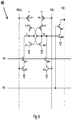
- the circuit 40 in Fig 4 improves the write port transistor size issue by modifying the circuit shown in Figure 1 to be ratioless during a write operation.
- the table in Fig 3 applies to circuit 40 in Fig 4 since the circuit 40 in Figure 4 has the same elements and operates in the same manner as the circuit 10 in Figure 1 , but has a ratioless write operation as described below.
- the cell 40 may also replace the cell 10 and be used seamlessly in the processing array 20 in Figure 2 .
- write port transistor M43, M44, M45 and M46 may be the same minimum size of transistor as PMOS transistors M49, M410, M411 and M412.
- the cell 40 size can be reduced and the write port is not affected by the write ratio.
- both WBLb and WBL are low to keep the cross coupled transistors M47, M48, M49 and M410 operating as the cross coupled latch of the SRAM cell 40.
- series transistor pair M49, M411 and M410, M412 can swap position to achieve the same function.
- M49 may have its gate tied to Db and is coupled to VDD and the source of M411 while M411 has its gate tied to WBLb that is coupled to D.
- series transistor pair M43, M45 and M44, M46 can swap position to achieve the same function.
- a ratioless write is performed with write bit line (WBL) or complementary write bit line (WBLb) to write the "0" node of the storage latch with its pull up transistor disabled and to write the "1" node of the storage latch with its pull up transistor enabled.
- WBL write bit line
- WBLb complementary write bit line
- the cell 40 in Fig 4 can be used in the processing array 20 in Fig 2 in the same way as cell 10 in Fig 1 .
- Figure 5 illustrates an implementation of a 3-port SRAM cell 50 that can perform basic Boolean operations, XOR and XNOR functions and ratioless selective write.
- the cell 50 has the same storage latch and write port circuitry as cell 40, therefore, the same ratioless selective write operation as cell 40.
- the cell 50 in Fig 5 adds another read port to the cell 40 in Fig 4 .
- Transistors M513 and M514 are added to form the second read port and an isolation circuit for that second read port.
- the complementary read word line REb may be coupled to the gate of transistor M513 that forms part of the read port while the complementary read bit line RBLb is coupled to the drain terminal of transistor M513.
- the gate of transistor M514 may be coupled to the D output from the cross coupled inverters and the source of transistor M514 may be coupled to ground.
- multiple cells can be turned on to perform an AND function between the complementary data stored in the cells that were turned on.
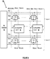
- FIG. 6 illustrates an implementation of a processing array 60 that has a plurality of the 3-port SRAM cells shown in Figure 5 in an array and split segments (Segment 1 and Segment 2 as shown) and each of the bit line (BL) read/write logic circuitry 64 (BL Read/Write Logic 0,..., BL Read/Write Logic n for each bit line) in the middle of each bit line.
- This processing array has a word line generator 62 that generates control signals (RF0, ..., REm, REb0, ..., REbm and WEO, ..., WEm) and each bit line has the two segments.
- segment 1 has RBLs1 and RBLs1b read bit lines (RBL0s1, ..., RBLns1 and RBL0s1b, ..., RBLns1b) with number of cells connected on it (cell 00, ...., cell 0n in the example in Figure 6 ) which are all connected to the BL read/write circuitry 64 and segment 2 has RBLs2 and RBLs2b lines (RBL0s2, ..., RBLns2 and RBL0s2b, ..., RBLns2b) with a number of cells (cell m0, ..., cell mn in the example in Figure 6 ) which are all connected to another input of the BL read/write circuitry 64.
- RBL0s1, ..., RBLns1 and RBL0s1b, ..., RBLns1b with number of cells connected on it (cell 00, ...., cell 0n in the example in Figure 6 ) which are all connected to the BL read/write circuitry 64
- the word line generator may generate one or multiple RE, REb signals in a cycle to turn on/activate one or more cells and the RBL, RBLb lines of the cells activated by the RE and REb signals form AND or NOR functions whose output is sent to the respective BL Read/Write Logic 64 for each bit line.
- Each BL Read/Write Logic 64 processes the RBL result (the result of the AND or NOR operation) and sends the results back to its WBL/WBLb for use/writing back to the same cell, or to the neighboring BL Read/Write Logic for use/writing back to the neighboring cell, or send it out of the processing array.
- the BL Read/Write logic 64 can store the RBL result from its own bit line or from the neighboring bit line in a latch within the BL Read/Write Logic so that, during a next or later cycle, the Read/Write logic can perform logic with the latched data that is the RBL result.
- the word line generator 62 generates one or more WE signals for the one or more cells into which data is to be written.
- the BL Read/Write Logic 64 processes the write data, either from its own RBL, or from the neighboring RBL, or from out of the processing array.
- the ability of BL Read/Write Logic 64 to process the data from the neighboring bit line means that the data can be shifting from one bit line to the neighboring bit line and one or more or all bit lines in the processing array may be shifting concurrently.
- the cells 40 and 50 described here are for computation memory applications, but these cells in Figures 4 and 5 can be operated as an SRAM cell with great noise immunity and ultralow VDD operation.
- the VDD operation level can be as low as the threshold voltage of NMOS and PMOS transistors of the cell.
- Isolated storage latch the read or write operation will not affect the stability of storage latch.
- the VDD operation level for storage is as low as the threshold voltage of NMOS and PMOS transistors for the cross coupled latch to be active.
- the read bit line voltage level will not affect the stability of the storage node.
- the read bit line is pre-charged high and be discharged by the turning on of the read port access transistors.
- the VDD operation level is as low as the threshold voltage of read port NMOS transistors.
- Ratioless write The writing to the storage latch occurs by just turning on the NMOS or PMOS transistors of the write port without write ratio.
- the VDD operation level is as low as the threshold voltage of write port NMOS and PMOS transistors.
- system and method disclosed herein may be implemented via one or more components, systems, servers, appliances, other subcomponents, or distributed between such elements.
- systems may include an/or involve, inter alia, components such as software modules, general-purpose CPU, RAM, etc. found in general-purpose computersP.
- components such as software modules, general-purpose CPU, RAM, etc. found in general-purpose computersP.
- a server may include or involve components such as CPU, RAM, etc., such as those found in general-purpose computers.
- system and method herein may be achieved via implementations with disparate or entirely different software, hardware and/or firmware components, beyond that set forth above.
- components e.g., software, processing components, etc.
- computer-readable media associated with or embodying the present inventions
- aspects of the innovations herein may be implemented consistent with numerous general purpose or special purpose computing systems or configurations.
- exemplary computing systems, environments, and/or configurations may include, but are not limited to: software or other components within or embodied on personal computers, servers or server computing devices such as routing/connectivity components, hand-held or laptop devices, multiprocessor systems, microprocessor-based systems, set top boxes, consumer electronic devices, network PCs, other existing computer platforms, distributed computing environments that include one or more of the above systems or devices, etc.
- aspects of the system and method may be achieved via or performed by logic and/or logic instructions including program modules, executed in association with such components or circuitry, for example.
- program modules may include routines, programs, objects, components, data structures, etc. that perform particular tasks or implement particular instructions herein.
- the inventions may also be practiced in the context of distributed software, computer, or circuit settings where circuitry is connected via communication buses, circuitry or links. In distributed settings, control/instructions may occur from both local and remote computer storage media including memory storage devices.
- Computer readable media can be any available media that is resident on, associable with, or can be accessed by such circuits and/or computing components.
- Computer readable media may comprise computer storage media and communication media.
- Computer storage media includes volatile and nonvolatile, removable and non-removable media implemented in any method or technology for storage of information such as computer readable instructions, data structures, program modules or other data.
- Computer storage media includes, but is not limited to, RAM, ROM, EEPROM, flash memory or other memory technology, CD-ROM, digital versatile disks (DVD) or other optical storage, magnetic tape, magnetic disk storage or other magnetic storage devices, or any other medium which can be used to store the desired information and can accessed by computing component.
- Communication media may comprise computer readable instructions, data structures, program modules and/or other components. Further, communication media may include wired media such as a wired network or direct-wired connection, however no media of any such type herein includes transitory media. Combinations of the any of the above are also included within the scope of computer readable media.
- the terms component, module, device, etc. may refer to any type of logical or functional software elements, circuits, blocks and/or processes that may be implemented in a variety of ways.
- the functions of various circuits and/or blocks can be combined with one another into any other number of modules.
- Each module may even be implemented as a software program stored on a tangible memory (e.g., random access memory, read only memory, CD-ROM memory, hard disk drive, etc.) to be read by a central processing unit to implement the functions of the innovations herein.
- the modules can comprise programming instructions transmitted to a general purpose computer or to processing/graphics hardware via a transmission carrier wave.
- the modules can be implemented as hardware logic circuitry implementing the functions encompassed by the innovations herein.
- the modules can be implemented using special purpose instructions (SIMD instructions), field programmable logic arrays or any mix thereof which provides the desired level performance and cost.
- SIMD instructions special purpose instructions
- features consistent with the disclosure may be implemented via computer-hardware, software and/or firmware.
- the systems and methods disclosed herein may be embodied in various forms including, for example, a data processor, such as a computer that also includes a database, digital electronic circuitry, firmware, software, or in combinations of them.
- a data processor such as a computer that also includes a database
- digital electronic circuitry such as a computer
- firmware such as a firmware
- software such as a computer
- the systems and methods disclosed herein may be implemented with any combination of hardware, software and/or firmware.
- the above-noted features and other aspects and principles of the innovations herein may be implemented in various environments.
- Such environments and related applications may be specially constructed for performing the various routines, processes and/or operations according to the invention or they may include a general-purpose computer or computing platform selectively activated or reconfigured by code to provide the necessary functionality.
- the processes disclosed herein are not inherently related to any particular computer, network, architecture, environment, or other apparatus, and may be implemented by a suitable combination of hardware, software, and/or firmware.
- various general-purpose machines may be used with programs written in accordance with teachings of the invention, or it may be more convenient to construct a specialized apparatus or system to perform the required methods and techniques.
- aspects of the method and system described herein, such as the logic may also be implemented as functionality programmed into any of a variety of circuitry, including programmable logic devices (“PLDs”), such as field programmable gate arrays (“FPGAs”), programmable array logic (“PAL”) devices, electrically programmable logic and memory devices and standard cell-based devices, as well as application specific integrated circuits.
- PLDs programmable logic devices
- FPGAs field programmable gate arrays
- PAL programmable array logic
- Some other possibilities for implementing aspects include: memory devices, microcontrollers with memory (such as EEPROM), embedded microprocessors, firmware, software, etc.
- aspects may be embodied in microprocessors having software-based circuit emulation, discrete logic (sequential and combinatorial), custom devices, fuzzy (neural) logic, quantum devices, and hybrids of any of the above device types.
- the underlying device technologies may be provided in a variety of component types, e.g., metal-oxide semiconductor field-effect transistor (“MOSFET”) technologies like complementary metal-oxide semiconductor (“CMOS”), bipolar technologies like emitter-coupled logic (“ECL”), polymer technologies (e.g., silicon-conjugated polymer and metal-conjugated polymer-metal structures), mixed analog and digital, and so on.
- MOSFET metal-oxide semiconductor field-effect transistor
- CMOS complementary metal-oxide semiconductor
- ECL emitter-coupled logic
- polymer technologies e.g., silicon-conjugated polymer and metal-conjugated polymer-metal structures
- mixed analog and digital and so on.
Landscapes
- Engineering & Computer Science (AREA)
- Microelectronics & Electronic Packaging (AREA)
- Computer Hardware Design (AREA)
- Theoretical Computer Science (AREA)
- Physics & Mathematics (AREA)
- General Engineering & Computer Science (AREA)
- General Physics & Mathematics (AREA)
- Static Random-Access Memory (AREA)
Applications Claiming Priority (1)
| Application Number | Priority Date | Filing Date | Title |
|---|---|---|---|
| US16/785,141 US10854284B1 (en) | 2016-12-06 | 2020-02-07 | Computational memory cell and processing array device with ratioless write port |
Publications (2)
| Publication Number | Publication Date |
|---|---|
| EP3863014A1 true EP3863014A1 (de) | 2021-08-11 |
| EP3863014B1 EP3863014B1 (de) | 2025-10-29 |
Family
ID=74556765
Family Applications (1)
| Application Number | Title | Priority Date | Filing Date |
|---|---|---|---|
| EP21155509.9A Active EP3863014B1 (de) | 2020-02-07 | 2021-02-05 | Rechnergesteuerte speicherzelle und verarbeitungsanordnungsvorrichtung mit verhältnislosem schreibport |
Country Status (3)
| Country | Link |
|---|---|
| EP (1) | EP3863014B1 (de) |
| CN (1) | CN113257305B (de) |
| TW (1) | TWI777404B (de) |
Citations (3)
| Publication number | Priority date | Publication date | Assignee | Title |
|---|---|---|---|---|
| US20120212996A1 (en) * | 2011-02-22 | 2012-08-23 | Setti Shanmukheswara Rao | Memory device having memory cells with write assist functionality |
| US20160254045A1 (en) * | 2013-12-30 | 2016-09-01 | The Regents Of The University Of Michigan | Static random access memory cell having improved write margin for use in ultra-low power application |
| US20180158519A1 (en) * | 2016-12-06 | 2018-06-07 | Gsi Technology, Inc. | Computational memory cell and processing array device using the memory cells for xor and xnor computations |
Family Cites Families (2)
| Publication number | Priority date | Publication date | Assignee | Title |
|---|---|---|---|---|
| US9640540B1 (en) * | 2016-07-19 | 2017-05-02 | Taiwan Semiconductor Manufacturing Co., Ltd. | Structure and method for an SRAM circuit |
| US10860318B2 (en) * | 2016-12-06 | 2020-12-08 | Gsi Technology, Inc. | Computational memory cell and processing array device using memory cells |
-
2021
- 2021-02-05 EP EP21155509.9A patent/EP3863014B1/de active Active
- 2021-02-05 TW TW110104531A patent/TWI777404B/zh active
- 2021-02-05 CN CN202110166435.3A patent/CN113257305B/zh active Active
Patent Citations (4)
| Publication number | Priority date | Publication date | Assignee | Title |
|---|---|---|---|---|
| US20120212996A1 (en) * | 2011-02-22 | 2012-08-23 | Setti Shanmukheswara Rao | Memory device having memory cells with write assist functionality |
| US20160254045A1 (en) * | 2013-12-30 | 2016-09-01 | The Regents Of The University Of Michigan | Static random access memory cell having improved write margin for use in ultra-low power application |
| US20180158519A1 (en) * | 2016-12-06 | 2018-06-07 | Gsi Technology, Inc. | Computational memory cell and processing array device using the memory cells for xor and xnor computations |
| US10249362B2 (en) | 2016-12-06 | 2019-04-02 | Gsi Technology, Inc. | Computational memory cell and processing array device using the memory cells for XOR and XNOR computations |
Also Published As
| Publication number | Publication date |
|---|---|
| CN113257305B (zh) | 2025-05-27 |
| TWI777404B (zh) | 2022-09-11 |
| TW202131328A (zh) | 2021-08-16 |
| CN113257305A (zh) | 2021-08-13 |
| EP3863014B1 (de) | 2025-10-29 |
Similar Documents
| Publication | Publication Date | Title |
|---|---|---|
| US11150903B2 (en) | Computational memory cell and processing array device using memory cells | |
| US10854284B1 (en) | Computational memory cell and processing array device with ratioless write port | |
| US11763881B2 (en) | Computational memory cell and processing array device using the memory cells for XOR and XNOR computations | |
| US11194548B2 (en) | Processing array device that performs one cycle full adder operation and bit line read/write logic features | |
| US10943648B1 (en) | Ultra low VDD memory cell with ratioless write port | |
| US10958272B2 (en) | Computational memory cell and processing array device using complementary exclusive or memory cells | |
| US10930341B1 (en) | Processing array device that performs one cycle full adder operation and bit line read/write logic features | |
| CN113205846A (zh) | 适用于高速内容寻址和存内布尔逻辑计算的sram单元 | |
| KR102172380B1 (ko) | 3진 메모리 셀 및 이를 포함하는 메모리 장치 | |
| Chen et al. | Configurable 8T SRAM for enbling in-memory computing | |
| US20250349349A1 (en) | Memory cell and method of operating the same | |
| Tsai et al. | Testing of in-memory-computing memories with 8 T SRAMs | |
| CN102054528A (zh) | 二进制内容可寻址存储器 | |
| Monga et al. | Design of in-memory computing enabled SRAM macro | |
| EP3863014B1 (de) | Rechnergesteuerte speicherzelle und verarbeitungsanordnungsvorrichtung mit verhältnislosem schreibport | |
| US20250349358A1 (en) | Associative processing cell with xnor+xor functions |
Legal Events
| Date | Code | Title | Description |
|---|---|---|---|
| PUAI | Public reference made under article 153(3) epc to a published international application that has entered the european phase |
Free format text: ORIGINAL CODE: 0009012 |
|
| STAA | Information on the status of an ep patent application or granted ep patent |
Free format text: STATUS: THE APPLICATION HAS BEEN PUBLISHED |
|
| AK | Designated contracting states |
Kind code of ref document: A1 Designated state(s): AL AT BE BG CH CY CZ DE DK EE ES FI FR GB GR HR HU IE IS IT LI LT LU LV MC MK MT NL NO PL PT RO RS SE SI SK SM TR |
|
| STAA | Information on the status of an ep patent application or granted ep patent |
Free format text: STATUS: REQUEST FOR EXAMINATION WAS MADE |
|
| 17P | Request for examination filed |
Effective date: 20220211 |
|
| RBV | Designated contracting states (corrected) |
Designated state(s): AL AT BE BG CH CY CZ DE DK EE ES FI FR GB GR HR HU IE IS IT LI LT LU LV MC MK MT NL NO PL PT RO RS SE SI SK SM TR |
|
| STAA | Information on the status of an ep patent application or granted ep patent |
Free format text: STATUS: EXAMINATION IS IN PROGRESS |
|
| 17Q | First examination report despatched |
Effective date: 20230420 |
|
| GRAP | Despatch of communication of intention to grant a patent |
Free format text: ORIGINAL CODE: EPIDOSNIGR1 |
|
| STAA | Information on the status of an ep patent application or granted ep patent |
Free format text: STATUS: GRANT OF PATENT IS INTENDED |
|
| INTG | Intention to grant announced |
Effective date: 20250221 |
|
| RIN1 | Information on inventor provided before grant (corrected) |
Inventor name: SHU, LEE-LEAN Inventor name: CHANG, CHAO-HUNG Inventor name: CHUANG, PATRICK |
|
| GRAJ | Information related to disapproval of communication of intention to grant by the applicant or resumption of examination proceedings by the epo deleted |
Free format text: ORIGINAL CODE: EPIDOSDIGR1 |
|
| STAA | Information on the status of an ep patent application or granted ep patent |
Free format text: STATUS: EXAMINATION IS IN PROGRESS |
|
| GRAP | Despatch of communication of intention to grant a patent |
Free format text: ORIGINAL CODE: EPIDOSNIGR1 |
|
| STAA | Information on the status of an ep patent application or granted ep patent |
Free format text: STATUS: GRANT OF PATENT IS INTENDED |
|
| INTC | Intention to grant announced (deleted) | ||
| INTG | Intention to grant announced |
Effective date: 20250528 |
|
| GRAS | Grant fee paid |
Free format text: ORIGINAL CODE: EPIDOSNIGR3 |
|
| GRAA | (expected) grant |
Free format text: ORIGINAL CODE: 0009210 |
|
| STAA | Information on the status of an ep patent application or granted ep patent |
Free format text: STATUS: THE PATENT HAS BEEN GRANTED |
|
| AK | Designated contracting states |
Kind code of ref document: B1 Designated state(s): AL AT BE BG CH CY CZ DE DK EE ES FI FR GB GR HR HU IE IS IT LI LT LU LV MC MK MT NL NO PL PT RO RS SE SI SK SM TR |
|
| REG | Reference to a national code |
Ref country code: CH Ref legal event code: F10 Free format text: ST27 STATUS EVENT CODE: U-0-0-F10-F00 (AS PROVIDED BY THE NATIONAL OFFICE) Effective date: 20251029 Ref country code: GB Ref legal event code: FG4D |
|
| REG | Reference to a national code |
Ref country code: IE Ref legal event code: FG4D |
|
| REG | Reference to a national code |
Ref country code: DE Ref legal event code: R096 Ref document number: 602021041107 Country of ref document: DE |
|
| REG | Reference to a national code |
Ref country code: NL Ref legal event code: MP Effective date: 20251029 |
|
| P01 | Opt-out of the competence of the unified patent court (upc) registered |
Free format text: CASE NUMBER: UPC_APP_0004342_3863014/2026 Effective date: 20260206 |
|
| PGFP | Annual fee paid to national office [announced via postgrant information from national office to epo] |
Ref country code: GB Payment date: 20260121 Year of fee payment: 6 |
|
| PG25 | Lapsed in a contracting state [announced via postgrant information from national office to epo] |
Ref country code: ES Free format text: LAPSE BECAUSE OF FAILURE TO SUBMIT A TRANSLATION OF THE DESCRIPTION OR TO PAY THE FEE WITHIN THE PRESCRIBED TIME-LIMIT Effective date: 20251029 |
|
| REG | Reference to a national code |
Ref country code: LT Ref legal event code: MG9D |
|
| PG25 | Lapsed in a contracting state [announced via postgrant information from national office to epo] |
Ref country code: NO Free format text: LAPSE BECAUSE OF FAILURE TO SUBMIT A TRANSLATION OF THE DESCRIPTION OR TO PAY THE FEE WITHIN THE PRESCRIBED TIME-LIMIT Effective date: 20260129 |
|
| PGFP | Annual fee paid to national office [announced via postgrant information from national office to epo] |
Ref country code: DE Payment date: 20260121 Year of fee payment: 6 |
|
| PG25 | Lapsed in a contracting state [announced via postgrant information from national office to epo] |
Ref country code: AT Free format text: LAPSE BECAUSE OF FAILURE TO SUBMIT A TRANSLATION OF THE DESCRIPTION OR TO PAY THE FEE WITHIN THE PRESCRIBED TIME-LIMIT Effective date: 20251029 Ref country code: FI Free format text: LAPSE BECAUSE OF FAILURE TO SUBMIT A TRANSLATION OF THE DESCRIPTION OR TO PAY THE FEE WITHIN THE PRESCRIBED TIME-LIMIT Effective date: 20251029 Ref country code: HR Free format text: LAPSE BECAUSE OF FAILURE TO SUBMIT A TRANSLATION OF THE DESCRIPTION OR TO PAY THE FEE WITHIN THE PRESCRIBED TIME-LIMIT Effective date: 20251029 |
|
| REG | Reference to a national code |
Ref country code: AT Ref legal event code: MK05 Ref document number: 1852613 Country of ref document: AT Kind code of ref document: T Effective date: 20251029 |
|
| PG25 | Lapsed in a contracting state [announced via postgrant information from national office to epo] |
Ref country code: NL Free format text: LAPSE BECAUSE OF FAILURE TO SUBMIT A TRANSLATION OF THE DESCRIPTION OR TO PAY THE FEE WITHIN THE PRESCRIBED TIME-LIMIT Effective date: 20251029 |
|
| PG25 | Lapsed in a contracting state [announced via postgrant information from national office to epo] |
Ref country code: RS Free format text: LAPSE BECAUSE OF FAILURE TO SUBMIT A TRANSLATION OF THE DESCRIPTION OR TO PAY THE FEE WITHIN THE PRESCRIBED TIME-LIMIT Effective date: 20260129 |
|
| PG25 | Lapsed in a contracting state [announced via postgrant information from national office to epo] |
Ref country code: IS Free format text: LAPSE BECAUSE OF FAILURE TO SUBMIT A TRANSLATION OF THE DESCRIPTION OR TO PAY THE FEE WITHIN THE PRESCRIBED TIME-LIMIT Effective date: 20260228 |
|
| PGFP | Annual fee paid to national office [announced via postgrant information from national office to epo] |
Ref country code: FR Payment date: 20260121 Year of fee payment: 6 |