EP3862844A1 - Systems and methods for memory system management based on thermal information of a memory system - Google Patents
Systems and methods for memory system management based on thermal information of a memory system Download PDFInfo
- Publication number
- EP3862844A1 EP3862844A1 EP21163241.9A EP21163241A EP3862844A1 EP 3862844 A1 EP3862844 A1 EP 3862844A1 EP 21163241 A EP21163241 A EP 21163241A EP 3862844 A1 EP3862844 A1 EP 3862844A1
- Authority
- EP
- European Patent Office
- Prior art keywords
- memory
- thermal
- regions
- memory system
- region
- Prior art date
- Legal status (The legal status is an assumption and is not a legal conclusion. Google has not performed a legal analysis and makes no representation as to the accuracy of the status listed.)
- Granted
Links
Images






Classifications
-
- G—PHYSICS
- G06—COMPUTING OR CALCULATING; COUNTING
- G06F—ELECTRIC DIGITAL DATA PROCESSING
- G06F12/00—Accessing, addressing or allocating within memory systems or architectures
- G06F12/02—Addressing or allocation; Relocation
- G06F12/0223—User address space allocation, e.g. contiguous or non contiguous base addressing
-
- G—PHYSICS
- G06—COMPUTING OR CALCULATING; COUNTING
- G06F—ELECTRIC DIGITAL DATA PROCESSING
- G06F1/00—Details not covered by groups G06F3/00 - G06F13/00 and G06F21/00
- G06F1/16—Constructional details or arrangements
- G06F1/20—Cooling means
- G06F1/206—Cooling means comprising thermal management
-
- G—PHYSICS
- G06—COMPUTING OR CALCULATING; COUNTING
- G06F—ELECTRIC DIGITAL DATA PROCESSING
- G06F1/00—Details not covered by groups G06F3/00 - G06F13/00 and G06F21/00
- G06F1/26—Power supply means, e.g. regulation thereof
- G06F1/32—Means for saving power
- G06F1/3203—Power management, i.e. event-based initiation of a power-saving mode
- G06F1/3234—Power saving characterised by the action undertaken
- G06F1/325—Power saving in peripheral device
- G06F1/3275—Power saving in memory, e.g. RAM, cache
-
- G—PHYSICS
- G06—COMPUTING OR CALCULATING; COUNTING
- G06F—ELECTRIC DIGITAL DATA PROCESSING
- G06F12/00—Accessing, addressing or allocating within memory systems or architectures
- G06F12/02—Addressing or allocation; Relocation
- G06F12/0223—User address space allocation, e.g. contiguous or non contiguous base addressing
- G06F12/023—Free address space management
-
- G—PHYSICS
- G06—COMPUTING OR CALCULATING; COUNTING
- G06F—ELECTRIC DIGITAL DATA PROCESSING
- G06F12/00—Accessing, addressing or allocating within memory systems or architectures
- G06F12/02—Addressing or allocation; Relocation
- G06F12/08—Addressing or allocation; Relocation in hierarchically structured memory systems, e.g. virtual memory systems
- G06F12/10—Address translation
-
- G—PHYSICS
- G06—COMPUTING OR CALCULATING; COUNTING
- G06F—ELECTRIC DIGITAL DATA PROCESSING
- G06F12/00—Accessing, addressing or allocating within memory systems or architectures
- G06F12/02—Addressing or allocation; Relocation
- G06F12/08—Addressing or allocation; Relocation in hierarchically structured memory systems, e.g. virtual memory systems
- G06F12/12—Replacement control
- G06F12/121—Replacement control using replacement algorithms
- G06F12/122—Replacement control using replacement algorithms of the least frequently used [LFU] type, e.g. with individual count value
-
- G—PHYSICS
- G06—COMPUTING OR CALCULATING; COUNTING
- G06F—ELECTRIC DIGITAL DATA PROCESSING
- G06F13/00—Interconnection of, or transfer of information or other signals between, memories, input/output devices or central processing units
- G06F13/14—Handling requests for interconnection or transfer
- G06F13/16—Handling requests for interconnection or transfer for access to memory bus
- G06F13/1668—Details of memory controller
-
- G—PHYSICS
- G06—COMPUTING OR CALCULATING; COUNTING
- G06F—ELECTRIC DIGITAL DATA PROCESSING
- G06F13/00—Interconnection of, or transfer of information or other signals between, memories, input/output devices or central processing units
- G06F13/14—Handling requests for interconnection or transfer
- G06F13/20—Handling requests for interconnection or transfer for access to input/output bus
- G06F13/24—Handling requests for interconnection or transfer for access to input/output bus using interrupt
-
- G—PHYSICS
- G06—COMPUTING OR CALCULATING; COUNTING
- G06F—ELECTRIC DIGITAL DATA PROCESSING
- G06F13/00—Interconnection of, or transfer of information or other signals between, memories, input/output devices or central processing units
- G06F13/38—Information transfer, e.g. on bus
- G06F13/42—Bus transfer protocol, e.g. handshake; Synchronisation
- G06F13/4282—Bus transfer protocol, e.g. handshake; Synchronisation on a serial bus, e.g. I2C bus, SPI bus
-
- G—PHYSICS
- G06—COMPUTING OR CALCULATING; COUNTING
- G06F—ELECTRIC DIGITAL DATA PROCESSING
- G06F3/00—Input arrangements for transferring data to be processed into a form capable of being handled by the computer; Output arrangements for transferring data from processing unit to output unit, e.g. interface arrangements
- G06F3/06—Digital input from, or digital output to, record carriers, e.g. RAID, emulated record carriers or networked record carriers
- G06F3/0601—Interfaces specially adapted for storage systems
- G06F3/0602—Interfaces specially adapted for storage systems specifically adapted to achieve a particular effect
- G06F3/0604—Improving or facilitating administration, e.g. storage management
-
- G—PHYSICS
- G06—COMPUTING OR CALCULATING; COUNTING
- G06F—ELECTRIC DIGITAL DATA PROCESSING
- G06F3/00—Input arrangements for transferring data to be processed into a form capable of being handled by the computer; Output arrangements for transferring data from processing unit to output unit, e.g. interface arrangements
- G06F3/06—Digital input from, or digital output to, record carriers, e.g. RAID, emulated record carriers or networked record carriers
- G06F3/0601—Interfaces specially adapted for storage systems
- G06F3/0628—Interfaces specially adapted for storage systems making use of a particular technique
- G06F3/0629—Configuration or reconfiguration of storage systems
- G06F3/0631—Configuration or reconfiguration of storage systems by allocating resources to storage systems
-
- G—PHYSICS
- G06—COMPUTING OR CALCULATING; COUNTING
- G06F—ELECTRIC DIGITAL DATA PROCESSING
- G06F3/00—Input arrangements for transferring data to be processed into a form capable of being handled by the computer; Output arrangements for transferring data from processing unit to output unit, e.g. interface arrangements
- G06F3/06—Digital input from, or digital output to, record carriers, e.g. RAID, emulated record carriers or networked record carriers
- G06F3/0601—Interfaces specially adapted for storage systems
- G06F3/0668—Interfaces specially adapted for storage systems adopting a particular infrastructure
- G06F3/0671—In-line storage system
- G06F3/0673—Single storage device
-
- G—PHYSICS
- G06—COMPUTING OR CALCULATING; COUNTING
- G06F—ELECTRIC DIGITAL DATA PROCESSING
- G06F9/00—Arrangements for program control, e.g. control units
- G06F9/06—Arrangements for program control, e.g. control units using stored programs, i.e. using an internal store of processing equipment to receive or retain programs
- G06F9/46—Multiprogramming arrangements
- G06F9/50—Allocation of resources, e.g. of the central processing unit [CPU]
- G06F9/5094—Allocation of resources, e.g. of the central processing unit [CPU] where the allocation takes into account power or heat criteria
-
- G—PHYSICS
- G11—INFORMATION STORAGE
- G11C—STATIC STORES
- G11C7/00—Arrangements for writing information into, or reading information out from, a digital store
- G11C7/04—Arrangements for writing information into, or reading information out from, a digital store with means for avoiding disturbances due to temperature effects
-
- G—PHYSICS
- G06—COMPUTING OR CALCULATING; COUNTING
- G06F—ELECTRIC DIGITAL DATA PROCESSING
- G06F2212/00—Indexing scheme relating to accessing, addressing or allocation within memory systems or architectures
- G06F2212/10—Providing a specific technical effect
- G06F2212/1016—Performance improvement
-
- G—PHYSICS
- G11—INFORMATION STORAGE
- G11C—STATIC STORES
- G11C11/00—Digital stores characterised by the use of particular electric or magnetic storage elements; Storage elements therefor
- G11C11/21—Digital stores characterised by the use of particular electric or magnetic storage elements; Storage elements therefor using electric elements
- G11C11/34—Digital stores characterised by the use of particular electric or magnetic storage elements; Storage elements therefor using electric elements using semiconductor devices
- G11C11/40—Digital stores characterised by the use of particular electric or magnetic storage elements; Storage elements therefor using electric elements using semiconductor devices using transistors
- G11C11/401—Digital stores characterised by the use of particular electric or magnetic storage elements; Storage elements therefor using electric elements using semiconductor devices using transistors forming cells needing refreshing or charge regeneration, i.e. dynamic cells
- G11C11/406—Management or control of the refreshing or charge-regeneration cycles
- G11C11/40626—Temperature related aspects of refresh operations
-
- Y—GENERAL TAGGING OF NEW TECHNOLOGICAL DEVELOPMENTS; GENERAL TAGGING OF CROSS-SECTIONAL TECHNOLOGIES SPANNING OVER SEVERAL SECTIONS OF THE IPC; TECHNICAL SUBJECTS COVERED BY FORMER USPC CROSS-REFERENCE ART COLLECTIONS [XRACs] AND DIGESTS
- Y02—TECHNOLOGIES OR APPLICATIONS FOR MITIGATION OR ADAPTATION AGAINST CLIMATE CHANGE
- Y02D—CLIMATE CHANGE MITIGATION TECHNOLOGIES IN INFORMATION AND COMMUNICATION TECHNOLOGIES [ICT], I.E. INFORMATION AND COMMUNICATION TECHNOLOGIES AIMING AT THE REDUCTION OF THEIR OWN ENERGY USE
- Y02D10/00—Energy efficient computing, e.g. low power processors, power management or thermal management
Definitions
- Memory systems are used in many electronic devices such as personal digital assistants (PDAs), laptop computers, mobile phones and digital cameras.
- Recent memory chip designs particularly those that use 3D-stacked structures, may exhibit increased data density and power density. With the use of multi-channel and sub-ranked memories, as well as partitioning of workloads across channels, it is possible for thermal hotspots to arise in the memory system.
- thermal management such as by energy management and resource sharing or workload fairness schemes to reduce or eliminate hotspots.
- request stream prioritization and transaction throttling mechanisms for energy management and resource sharing or workload fairness schemes.
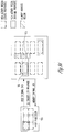
- FIG. 1 is a diagram illustrating a system 100 in which example embodiments may be implemented.
- the system 100 may include a processor 110 coupled to a memory controller 120 through a first bus 121.
- the memory controller 120 may be coupled to a memory system 125 through a second bus 122.
- the memory controller 120 may execute memory transaction requests from the processor 110.
- the memory controller 120 may transfer data between the processor 110 and the memory system 125 over the first and second buses 121 and 122.
- the first bus 121 and the second bus 122 may employ a known protocol to connect the processor 110 to the memory controller 120 and to connect the memory controller 120 to the memory system 130.
- Some examples of system 100 may include personal computers, laptop computers, personal digital assistants (PDAs), digital cameras, electronic games, digital media player/records, and the like.
- PDAs personal digital assistants
- the memory system 130 may comprise one or more physical devices (not shown) each comprised of one or more physical channels (not shown) that are mapped to regions according to a data structure, hereinafter referred to by example as a "table", stored in a map RAM 140 of the memory controller 120.
- a region can be a channel, bank, vault, group, or any other grouping in a memory system.
- the map RAM 140 may store temperatures of regions of memory cells as described below with respect to FIG. 2 .
- the memory controller 120 may include logic to map a logical memory address, received from the processor 110 in a memory allocation request, to a block address of a region based on the temperatures stored in the map RAM 140.
- the memory system 130 may include a hybrid memory cube (HMC) system of stacked memory dies though example embodiments are not limited thereto.
- HMC hybrid memory cube
- Instructions 145 may execute an operating system (OS) and one or more applications on the processor 110.
- the OS may request memory in the memory system 130 on behalf of the one or more applications.
- the memory controller 120 may map applications to physical locations in the memory system 130.
- Current address mapping and memory configuration systems may be designed in view of performance or power requirements. These or other systems may not provide a mechanism by which a memory system 130 can influence the data allocation choices of host processors 110, inform host processors 110 of events such as thermal emergencies, or provide thermal profiles to other thermally-connected elements.
- the processor 110 or the memory controller 120 may use on-die thermal sensors and thermal models to direct how data is mapped and relocated. In some example embodiments, the processor 110 or the memory controller 120 may use on-die thermal sensors and thermal models to individually adjust memory cell refresh across regions based on their temperature.
- FIG. 2 is a diagram of a memory system 200 according to various embodiments.
- the memory system 200 may serve functions of the memory system 130 ( FIG. 1 ).
- the memory system 200 may comprise memory dies 210 and 220. While two memory dies are illustrated, the memory system 200 may include fewer or more than two memory dies.
- the memory dies 210 and 220 may include two or more regions of memory cells. Two or more of the plurality of regions of memory cells may each include a thermal sensor (TS) for sensing a temperature of a corresponding region of memory cells.
- TS thermal sensor
- the memory system 200 may include independent logic and memory dies, dies stacked via silicon interposers or directly stacked dies ("3D stacking"), or any other arrangement of logic and storage dies.
- thermal sensors may be included in the logic die 230, in one or more memory dies, or in both logic die 230 and memory dies 210 and 220.
- Each of the plurality of memory dies may include at least one TS.
- Each of the plurality of memory dies may include a TS situated in each region of the memory die.
- Each of the TSs may transmit information to each other of the plurality of memory dies, and each of the TSs may transmit information to thermal control logic (TCL).
- TCL thermal control logic
- the number of TSs may be determined based on die size, thermal gradient, and required resolution for temperature sensing. If a higher resolution is required, more TSs may be used. If a lower resolution is sufficient, then fewer TSs may be used.
- TCL Temperature Control Logic
- the TCL may read the state of the thermal sensors and can be used to adjust the refresh rates of each region based on the temperature of that region.
- the TCL may read a plurality of thermal sensors, at least two of the plurality of thermal sensors corresponding to different regions of memory cells.
- the TSs may be read by external logic via an external interface.
- Each type of memory or storage may be managed separately by separate TCL or other control logic.
- the TCL may indicate hot spots by transmitting thermal information to the host Operating System executing on the host processor 110 ( FIG. 1 ).
- the TCL may further indicate hot spots to the mapping logic of the memory controller 120 such that the memory controller 120 may avoid mapping to the hot spots.
- the TCL may further receive thermal information from either or both the host processor 110 or the memory controller 120.
- the TCL block may reside on one or more of the memory dies 210 or 220.
- the memory controller 120 or other block may read the data from the TCL or the TCL may transmit the required changes to the processor 110. This transmission may be achieved using the standard protocol to read registers in the memory, with the use of interrupt signals, or special IO added to the memory system 130 to allow the transition of the required information such as a simple serial interface.
- the TCL may reside in any location, including separate logic or memory die of the memory system 130.
- the TCL may continuously monitor the TSs or the TCL may sample the state of the TSs periodically. For example, the TCL may sample TS state every few micro-seconds (uS).
- Example embodiments may provide more than one, or multiple, TS sampling algorithms. For instance, when the memory system 130 is relatively cool, power may be saved by only sampling the temperature sensors periodically, for example, eight times per second. When a temperature sensor reports a hot rating the algorithm can be updated to sample that sensor more frequently.
- the sampling rate may be determined by how quickly the device(s) 130 can change temperature. Devices and systems that can change quickly over time will require faster sampling, devices or systems that change temperature slower can be sampled more slowly.
- the TCL logic may track the state of each TS.
- the states can vary from design to design and system to system in different example embodiments.
- Example embodiments may control the refresh rate of memory cells based on temperature.
- the entire memory system 130 is not treated the same with respect to control of refresh rates.
- each region may be refreshed individually based on the temperature of that region and not the worst-case temperature at any given location of the device.
- Table 1 is an example of how the Temperature Gradient Categories may be used to control refresh: Table 1 Category Refresh Rate Cold 1/8x Cool 1/4x Room Temp 1/2x Warm 1x Hot1x 1x Hot2x 2x Hot3x 4x Hot4x N/A - device damaged
- the refresh rate may change for each channel or region of memory independently, based on the sample taken from the local temperature sensor.
- Warm and Hot1x receive the same refresh rate, the rate specified in the device specification.
- the samples show the device is in the Cold region the device or channel receives only 1/8 the normal refresh commands because the retention of the device is better when cold.
- the sample from the TS identifies the temperature is in the Hot2x region the device, or channel will be refreshed twice as fast as specified.
- Table 1 is just an example, and the refresh rate varaiation may depend on the memory type and system implementation.
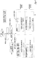
- FIG. 3 is a flow diagram illustrating a method 300 for setting refresh rates according to various embodiments.
- Thermal Control Logic ( FIG. 2 ) may read temperature values periodically, from thermal sensors, of a plurality of regions of the memory system 130.
- the Thermal Control Logic may set a refresh rate for each of the plurality of regions of the memory system based on the temperatures.
- the TCL may adjust time intervals between readings based on the temperature values.
- the TCL may reduce the time intervals between readings upon a reading of a large change in temperatures and the TCL may increase the time intervals between readings if the temperatures remain unchanged over a number of readings.
- the TCL may transmit readings from a first memory region to a second memory region and from the second memory region to the first memory region.
- the TCL may help perform allocation and migration decisions based on the transmitted readings.
- Example embodiments may provide methods to physically place data in memories to improve performance or power usage or to satisfy other system constraints.
- Mechanisms discussed with respect to example embodiments include address decoder-level (e.g., hardware) mapping changes as well as host operating system (e.g., software) memory allocation policies.
- Hot spots of a system may be characterized prior to the actual use of the system. Hot spots may be located around areas of high throughput compute, interface, or analog blocks that draw a lot of current. These hot spots may not always be “hot” depending on which application or function is being performed in the system but these are areas that are known to become hot based on the functionality the device is going to perform. These hot spots generally transfer heat to the adjacent die, in this example the other die is considered to be DRAM but could be any other memory or logic type.
- Processors 110 supporting Virtual Memory may introduce a level of indirection between requested memory locations and their physical addresses. However, the target physical addresses may be re-mapped again into memory channel, rank, bank, row and column control signals without regard for thermal or other physically non-uniform regions.
- Memory controllers 120 typically scramble the logical to physical address mappings to achieve better performance or power characteristics. Example embodiments may add the thermal map knowledge to the mapping process.
- hardware implemented in the memory controller 120 may utilize the pre-characterized and runtime (dynamic) thermal data to remap the physical locations such that the hot spots are in a known region of the map.
- this known hot region may be the last memory to be assigned, thus if there is any available memory with a cooler temperature map those regions may be used first.
- the hot regions may be assigned the least frequently accessed logical addresses.
- the monitoring and remapping facilities of example embodiments may migrate data accordingly, to different regions than the ones originally assigned.
- the mapping solution of example embodiments may be performed in hardware or software.
- the operating system executing on a host processor 110 may maintain a list of free physical pages which can be selected to hold newly allocated data.
- An enhanced operating system may continuously update the free page list in order of lowest to highest temperature.
- the updates may be hardware-assisted, whereby the memory controller 120 or other hardware maintains the hot/cold free list in its own reserved storage area (e.g. SRAM, Flash, PCM or a reserved DRAM region), for example map RAM 140 ( FIG. 1 ).
- the address map may be manipulated in a virtualized system via memory management systems, for example, memory management code that may make allocation decisions (and periodically, remapping decisions) based on real-time feedback on region temperature.
- example embodiments may use an Intermediate Address Map (IAM).
- IAM may provide another level of indirection between physical addresses entering the memory controller 120, and the main memory (e.g. DRAM) addresses actually used.
- Some memory systems may have hot components in the stacked controller die (e.g. I/O interfaces or channel controllers). Because of the hot components, applying dynamic address mapping according to example embodiments may balance transactions across all physical I/O links at runtime, removing hotspots.
- hot components e.g. I/O interfaces or channel controllers.
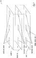
- FIG. 4 is a diagram of a physical dynamic random access memory (DRAM) floor plan according to various embodiments.
- FIG. 4 illustrates how the physical address space may be subdivided into large 'uniform regions' relating to the physical placement of the uniform regions. This address translation may occur within a memory controller 120 ( FIG. 1 ) enhanced with static and runtime thermal information. The same techniques may be used for mapping between non-uniform memory regions such as those with different latencies and bandwidths.
- memory die may include banks of addresses operating with different latencies, so thermal information according to example embodiments could indicated to the host processor 110 as permanently 'cold' regions for allocating the most heavily used data.
- a host processor 110 may provide virtual addresses to a translation lookaside buffer (TLB).
- TLB translation lookaside buffer
- the TLB may store a mapping between a virtual address, which is the address of a process executing on the host processor 110, and the physical addresses, which are natural physical locations in the memory system.
- a virtual address which is the address of a process executing on the host processor 110
- the physical addresses which are natural physical locations in the memory system.
- the physical address may be provided by the TLB to the memory controller 120 and the memory controller 120 may do a further level of remapping to map the physical address to the structure inside the memory system 130, for example to memory system rows, columns, banks, channels, etc.
- FIG. 4 depicts two mapping schemes that may be implemented by the memory controller 120 when the memory controller 120 maps the physical address from the TLB to locations in the memory system 130.
- coarse-grained physical region mapping for single-rank and double-rank regional Depth Mapping modes may be implemented in accordance with some embodiments.
- first mapping scheme implemented in the top row of thermal regions of the memory system 130, memory locations are mapped to be physically adjacent to each other in the memory.
- a first set of addresses is mapped in region Mem[0], then the next set of physical addresses is mapped to region Mem[1] and so forth down to Mem[N/4-1].
- the region Mem[N/4] in the adjacent thermal region is mapped to the next set of physical addresses.
- the memory controller 120 may implement both the first and the second mapping scheme together, or the memory controller 120 may implement one or the other of the first mapping scheme and the second mapping scheme.
- the processor 110 or the memory controller 120 may use a memory request throttling mechanism to shape memory activity and to remove thermal hotspots temporarily while the memory controller 120 performs data re-mapping. These and other embodiments may reduce or eliminate the occurrence of memory failure or degradation when sudden thermal events do not leave sufficient time for a data migration, or when thermal events are too short for implementation of data migration and re-mapping.
- the memory controller 120 may turn off (e.g., disable) data accesses to certain channels, banks or regions of the memory. The memory controller 120 may migrate data from those memory cells to other memory cells to remove the need to refresh those memory cells and to minimize or reduce power consumption in the region including those memory cells.
- the memory controller 120 may perform transaction throttling.
- request prioritization may allow more memory transaction requests from different sources.
- Transaction throttling in some embodiments may allow memory and logic thermal hotspots to be controlled or moved by reducing switching activity in the logic or memory being targeted.
- requests may be reduced to a hot area of a 3D-stacked memory controller and DRAM die such as the Micron HMC.
- the activity of a hot core may be indirectly throttled in a 3D-stacked compute and DRAM die by limiting its request bandwidth. This indirect throttling may reduce the temperature of memory components directly above the core, allowing the components to be refreshed less frequently.
- the memory addresses being throttled may be in entirely different physical locations in the DRAM die.
- Throttling may be performed at different granularities within the memory device. In order of increasing complexity, throttling may be done at the channel or vault level, the rank level, the bank level, the sub-bank level, or the row or column level in a memory device.
- the memory controller 120 may perform throttling. In some embodiments, throttling may be performed outside the memory controller 120 when an appropriate command protocol is present (which allows the target memory 130 ( FIG. 1 ) to assert back-pressure or deny requests). Using JEDEC-like protocols, the target memory 130 may implement throttling using the error-detection mechanism. When the memory 130 wants to ignore requests, the memory 130 may a fake memory error (e.g. CRC or ECC error). The host processor 110 may then re-try the request at a later time.
- an appropriate command protocol which allows the target memory 130 ( FIG. 1 ) to assert back-pressure or deny requests).
- JEDEC-like protocols the target memory 130 may implement throttling using the error-detection mechanism.
- the memory 130 may a fake memory error (e.g. CRC or ECC error).
- the host processor 110 may then re-try the request at a later time.
- the command protocol for a memory system 130 may include the on-die or off-die memory controller 120, may include a priority level.
- the priority level may support a level of indirection, whereby an identifier associated with a memory request initiates a table lookup (see Table 2).
- the table may be programmable by special commands.
- the lookup may indicate minimum and maximum bandwidth limits, along with maximum latency values. Separate limits may be specified for reads and writes, and there may be a set of hard limits and soft ('preferred') limits. The hard limits may be used to support performance-critical or real-time workloads.
- Table 2 Priority characteristics table.
- This table may be programmable and may be used by the host system(s) to indicate mandatory and desired characteristics of transaction streams as indicated by a per-transaction "Priority ID" field.
- Priority ID READ WRITE Hard Limit Soft Limit Hard Limit Soft Limit Min BW Max BW Max Lat Min BW Max BW Max Lat Min BW Max BW Max Lat Min BW Max BW Max Lat Min BW Max BW Max Lat Min 0 1 ...
- External messages or signals may be provided to the host processor 110 when these limits are violated, and the current status of runtime bandwidth and latency, per Priority ID, may be queried at any time.
- the mechanisms by which memory controllers 120 enforce the transaction priority characteristics may include, but are not restricted to: per-priority mode counters that monitor request bandwidth and latency; periodic, incremental adjustment of knobs to approach the target limits, where the knobs may include the number of memory controller buffer entries allocated to each Priority ID or counters in the command arbiter and selection units to change relative priorities; ignoring Priority ID groups well within their limits while adjusting knobs of Priority ID groups that are close to their limits; and runtime adjustment of memory controller 120 settings using a host processor 110 thread, a dedicated microcontroller, or custom logic.
- the memory controller 120 may further throttle the number of transactions that issue to the 'hot' region by limiting or slowing the accesses to the region.
- Transaction throttling may also be used with versions of the ARM Advanced Extensible Interface (AXI) bus virtualization protocol.
- the virtualization protocol may give each processor 110 or set of processors 110 its own network ID. Accordingly, several processors 110 in a system 100 may share the same physical bus or buses and queues but the processors 110 may continue to have different arbitration results and slave-way responses based on the virtual network to which the processor 110 belongs.
- the memory controller 120 may reduce the queue entries associated with that network to reduce the request rate without having to use software intervention or adding sideband signals back to the processor 110. In this manner, the memory controller 120 may shape the traffic targeting only the hot spot(s) without affecting traffic that targets cooler or cold regions leaving those regions to operate at their pre-determined operating points.
- FIG. 5 is a flow diagram of a method 500 for throttling memory transactions in accordance with at least one embodiment.
- a memory controller 120 may receive a request for a memory transaction accessing a location within a physical memory region.
- the request may be received from, for example, a host processor 110 ( FIG. 1 ).
- the memory controller 120 may retrieve a priority level of the request.
- the memory controller 120 may retrieve the priority level from a table similar to the Table 2 discussed previously.
- the table may be programmable by special commands, and the table may indicate minimum and maximum bandwidth limits, along with maximum latency values. Separate limits may be specified for reads and writes, and there may be a set of hard limits and soft ('preferred') limits. The hard limits may be used to support performance-critical or real-time workloads.
- the memory controller 120 may reserve a bandwidth for the memory transaction based on the priority level of the request and based on a temperature of the physical memory region.
- the method 500 may further include determining that the physical memory region is in a first temperature state, inhibiting the request from accessing the location based on the determining, and transmitting an error message to a host processor 110 to notify of the inhibiting.
- Throttling as discussed above, may be implemented using current bus interface standards such as the ARM AXI bus virtualization protocol.
- a host processor 110 may obtain the thermal physical characteristics of an external (3D stacked or otherwise) device, for example the memory system 130 ( FIG. 1 ).
- the host processor 110 may obtain the thermal information from the memory controller 120 or map RAM 140 of the memory controller.
- Thermal information may include a graph, for example a data structure, of material regions along with the regions' location in space, and the regions' thermal capacitance and resistance (RC) properties.
- the thermal information may also be specified at a higher level, for example by a separate software application for collecting and dispensing thermal information. For example the static thermal properties of the devices may be loaded from software rather than a hardware table.
- a memory controller 120 may protect thermal information via encryption or through the need for a privileged memory request, through a read from a reserved region of addresses, or through reads via a separate data channel (e.g. a simple serial interface).
- the host processor 110 may use thermal information communicated by the memory controller 120 to the host processor 110 to allocate (and re-allocate as temperature changes) memory pages in a priority order.
- the host processor 110 may implement a priority order according to one of at least two alternatives. In a first alternative, the most frequently-accessed pages may be allocated to the coolest regions. In at least these embodiments, heat may be spread out from I/O, sense-amp and other access logic into areas with more thermal headroom.
- the most frequently-accessed pages may be allocated to the hottest regions.
- a host processor 110 may implement this alternative because the hot regions in some volatile memories such as DRAM may require more frequent refresh operations than cold regions. By pushing memory activity to those regions, fewer explicit refresh commands need to be sent to those regions, as page open and close activity serves as a refresh.
- Some embodiments may implement an additional "upload" mechanism whereby information such as thermal limits (for a remote memory controller 120), thermal properties or dynamic temperature measurements of a host processor 110 die (or any other nearby die) can be sent by the host processor 110 to the units, dies, or regions of the memory system 130.
- the host processor 110 may store the settings or measurements may be stored in a memory of the host processor 110 and the host processor 110 may send the settings or measurements to the memory controller 120.
- the memory controller 120 may use this information to direct transaction throttling or data movement operations.
- micro-code or other executable instructions for implementing thermal control policies, throttling policies or other memory controller 120 behaviors can be sent to the memory system 130.
- the host processor 110, the memory controller 120, and the memory system 130 may share thermal data during a power up or during periodic sharing.
- nearby dies may communicate their static thermal properties and dynamic thermal sensor data to each other. This sharing may support data and thread placement (allocation) and migration (movement) decisions. The sharing may occur between any types of component in the system 100, not merely between compute and memory dies.
- the memory controller 120 may provide hardware support for operating system page allocation and migration mechanisms.
- an in-memory copy command may be provided by the memory controller 120 to perform internal transfers of thermal information that without using external bus resources.
- a map RAM 140 (SRAM/DRAM etc.), may be controlled by the memory controller 120 may provide a 'free list' of the coolest page addresses that should be allocated next.
- the map RAM 140 may alternatively or additionally be controlled by, for example, thermal control logic (TCL), the host processor 110, or a software application.
- TTL thermal control logic
- the map RAM 140 may be addressable by the host processor or host processors 110 (via appropriate mutual exclusion or lock mechanisms). To avoid providing already-allocated free list entries to the host processor 110, the memory controller 120 may have access to the host page table structures maintained by the host processor 110. The memory controller 120 may query the host page table structures to see if the host processor 110 has mapped a page.
- Example embodiments may further provide a "memory interrupt" signal or message that allows the memory system 130 or an external memory controller 120 to notify the host processor 110 or thermally-connected devices of thermal events. For example, if a memory region has too many errors, has too high a refresh frequency or has become a thermal hotspot, nearby devices or a controlling host processor 110 can be notified to take evasive action (re-mapping data, throttling frequency/voltage, migrating code to other cores etc.).
- evasive action re-mapping data, throttling frequency/voltage, migrating code to other cores etc.
- Example embodiments may include mechanisms for control logic to query memory devices on their temperature, to set thermal limits on memory devices, to communicate thermal maps and notification of status and thermal emergencies to connected control or processing logic.
- Memory devices for example the memory system 130, may communicate their physical thermal properties to an external processing unit, for example the memory controller 120 or the host processor 110. In this manner, thermal management mechanisms already implemented on the processor 110 can build a thermal model for temperature prediction, independent of the type of memory device actually connected to it.
- the memory device can provide other static information indicating the energy and power implications of certain controller actions to the processor 110 or the memory controller 120.
- the static information may include a table of absolute or relative energy, power or power density, as a function of request bandwidth, size, page hit rate or other measurable traffic features.
- FIG. 6 illustrates cooperate host memory data activity mapping in accordance with some embodiments.
- the host processor 610 may be operative to serve the functions of the host processor 110 ( FIG. 1 ).
- the memory system 630 may serve the functions of the memory system 130 ( FIG. 1 ).
- the memory system 630 may include 3D-stacked memory dies but example embodiments are not limited thereto.
- the memory system 630 may include a controller logic layer for example a logic die.
- the logic die may be stacked directly under the memory chips. All or some of the memory controller 120 logic may be implemented in the logic die.
- Regions such as regions 650 and 655 may be statically-defined hot regions or regions that are expected to get hot.
- Regions 660 and 665 are regions measured as hot in real-time by temperature sensors ( FIG. 2 ).
- the thermal information for the regions may be stored in the map RAM 140 ( FIG. 1 ).
- the bidirectional arrow 670 shows that the host processor 610 can both read temperature information from the memory system 630 and provide host
- the host processor 610 may create hot spots and the host processor 610 may communicate this information to other thermally-connected devices.
- the memory system 630 may likewise inform the host processor 610 of thermal conditions, including the static map stored in the map RAM 140 ( FIG. 1 ) and dynamic thermal information measured by temperature sensors ( FIG. 2 ).
- FIG. 7A depicts a similar system to FIG. 6 , in which the host processor 710 has produced a hot spot 750 that overlaps a hot spot 751 in the memory system 730. Accordingly, in FIG. 7B , the host processor 710 or the memory controller 120 ( FIG. 1 ) may move the hot spot 751 so that the hot spot 751 no longer overlaps with hot spot 750. The host process 710 or the memory controller 120 may copy data from its original location and update the map RAM 140 ( FIG. 1 ) to reflect the new mapped region of hot spot 751.
- FIG. 8 depicts a similar system as that described above with respect to FIG. 6-7 .
- the host processor 110 may migrate code, rather than data as discussed above with respect to FIG. 7 , to another host processor 110 (for multi-processor systems).
- FIG. 9 depicts a similar system as described above with respect to FIG. 6-8 .
- memory address regions 955 are migrated to be away from the hot spot 960.
- FIG. 10 is a flow diagram illustrating a method 1000 for mapping memory in accordance with some embodiments.
- a memory controller 120 may receive a memory allocation request from a host processor 110.
- the memory allocation request may include a first logical memory address.
- the memory controller 120 may map the first logical memory address to the block address in a first memory region of the memory system based on thermal data for memory regions of the memory system.
- the first memory region may have a lowest temperature of the memory regions of the memory system 130.
- the thermal data may be received from thermal sensors discussed above with respect to FIG. 2 .
- the method 1000 may further include mapping a second logical memory address to a second memory region.
- the second memory region may have a higher temperature than the first memory region.
- the method 1000 may further include storing the thermal data in a table in, for example, the map RAM 140 ( FIG. 1 ).
- the method 1000 may further include storing a default value for thermal data for each of the memory regions in the memory system 130. The default value may be based on a characteristic of each of the memory regions.
- the method 1000 may further include updating thermal data in the table in the map RAM 140 based on a sensed temperature during operation of the memory regions.
- the method may further include remapping the first logical memory address to a block address in a second memory region based on the updated thermal data. The remapping may comprise copying data from the first memory region to the second memory region as discussed above with respect to FIG. 6 .
- the method 1000 may further include mapping physical data corresponding to the first logical memory address across two or more memory regions of the memory system and accessing physical data in each of the two or more memory regions.
- the memory controller 120 may interleave addresses across regions, as shown in the second mapping scheme discussed above with respect to FIG. 4 .
- the interleaving of the lower two regions may make it more costly to migrate data to other regions if either of the two regions become hot. Interleaving of the type shown in the lower two regions of FIG. 4 may safely be performed if the static thermal map indicates that both regions are likely to be of equal temperature.
- FIG. 11 is a flow diagram illustrating a method 1100 for allocating memory according to various embodiments.
- the host processor 110 may query a table for temperatures of regions of the memory system 130.
- the table may be stored in the map RAM 140 as discussed above with respect to FIG. 1-2 .
- the host processor 110 may create an ordered list of regions of the memory system based on the temperatures of the regions retrieved form the table in, for example, the map RAM 140.
- the ordered list may further be ordered based on a physical location of the regions of the memory system 130.
- the host processor 110 may request allocation to a region based on a position of the region in the ordered list. For example, the host processor 110 may first allocate to the coldest region on the list. The request may further be based on a characteristic of the process. For example, some processes may require a certain amount of bandwidth or specific energy requirements for process data. As another illustrative example, some processes may be allocated to a hotter region if refresh operations are expected to occur more frequently for that process.
- the operation 1100 may further include receiving an indication that the temperatures of the region have changed.
- the processor 110 or memory controller 120 may receive indications on temperatures as discussed above with respect to FIG. 6-9 .
- the processor 110 may reorder the ordered list based on the updated temperatures.
- the processor 110 may remap a logical address corresponding to the allocation from a first memory region to a second memory region based on receiving updated temperature information.
- the remapping including copying data from the first memory region to the second memory region.
- the processor 110 may perform remapping of code or data, as discussed above with respect to FIG. 6-9 .
- the apparatus of various embodiments includes or can be included in electronic circuitry used in high-speed computers, communication and signal processing circuitry, memory modules, portable memory storage devices (e.g., thumb drives), single or multi-processor modules, single or multiple embedded processors, multi-core processors, data switches, and application-specific modules including multilayer, multi-chip modules.
- Such apparatus may further be included as subcomponents within a variety of electronic systems, such as televisions, memory cellular telephones, personal computers (e.g., laptop computers, desktop computers, handheld computers, tablet computers, etc.), workstations, radios, video players, audio players (e.g., MP3 (Motion Picture Experts Group, Audio Layer 3) players), vehicles, medical devices (e.g., heart monitor, blood pressure monitor, etc.), set top boxes, and others.
- televisions e.g., laptop computers, desktop computers, handheld computers, tablet computers, etc.
- workstations e.g., radios, video players, audio players (e.g., MP3 (Motion Picture Experts Group, Audio Layer 3) players), vehicles, medical devices (e.g., heart monitor, blood pressure monitor, etc.), set top boxes, and others.
- video players e.g., laptop computers, desktop computers, handheld computers, tablet computers, etc.
- audio players e.g., MP3 (Motion Picture Experts Group, Audio
- Some embodiments may include a machine-readable medium on which is stored one or more sets of instructions (e.g., software) embodying any one or more of the methodologies or functions described herein.
- the instructions may reside, completely or at least partially, within the processor 110 or the memory controller 120 ( FIG. 1 ) during execution thereof by the system 100, with the processor 110 and the memory controller 120 also constituting machine-readable media.
- the machine-readable medium when executed on the processor 110, may cause the processor 110 to maintain a list of available regions of a memory system 130.
- the list may be in an order based on temperatures of the available regions.
- the temperatures may be default temperatures based on a predicted temperature of the corresponding available region.
- the predicted temperature may be based on a physical characteristic of the corresponding available region.
- the computer-readable medium may further cause the processor 110 to request an allocation, to a process executing on the processor 110, of a first block address in a first available region in the list based on the order of the first available region in the list and further based on a characteristic of the process.
- the machine-readable medium may cause the processor 110 to receive update temperature data from, for example, the map RAM 140 ( FIG. 1 ) from the memory controller 130, or from temperature sensors in the memory system 130.
- the machine-readable medium may cause the processor 110 to reorder the list based on the updated temperature data and allocate a second process to be mapped to a second block address in a second available region of the memory system 130 based on the reordered list.
- Example embodiments described herein may provide control of memory refresh rates in the presence of activity hotspots.
- Example embodiments may provide increased thermal headroom for performance-boosting techniques where clock frequency is boosted when most compute units are idle by moving data away from the hot core or by throttling its memory bandwidth.
- memory bandwidth throttling and data re-mapping from hot memory regions described with respect to example embodiments may be entirely under the control of the memory logic. Accordingly, example embodiments may permit the memory vendor to use proprietary sensors embedded in memory to avoid thermal hazards.
- Example embodiments may use a memory controller stack layer of a hybrid memory cube (HMC) or other memory that is not stacked with the host processing device, to provide thermal control.
- HMC hybrid memory cube
- the machine-readable medium may be a single medium or may be multiple media (e.g., a centralized or distributed database, and/or associated caches and servers) that store the one or more sets of instructions.
- Machine-readable medium may include any non-transitory medium that is capable of storing, encoding, or carrying a set of instructions of execution by the machine.
- machine-readable medium may include solid-state memories, optical media, or magnetic media.
Landscapes
- Engineering & Computer Science (AREA)
- Theoretical Computer Science (AREA)
- Physics & Mathematics (AREA)
- General Engineering & Computer Science (AREA)
- General Physics & Mathematics (AREA)
- Human Computer Interaction (AREA)
- Software Systems (AREA)
- Memory System (AREA)
- Techniques For Improving Reliability Of Storages (AREA)
- Dram (AREA)
- Microelectronics & Electronic Packaging (AREA)
- Computer Hardware Design (AREA)
Abstract
Description
- This application claims the benefit of priority to U.S. Application Serial No.
14/055,672, filed 16 October 2013 U.S. Provisional Application No. 61/791,673, filed 15 March 2013 - Memory systems are used in many electronic devices such as personal digital assistants (PDAs), laptop computers, mobile phones and digital cameras. Recent memory chip designs, particularly those that use 3D-stacked structures, may exhibit increased data density and power density. With the use of multi-channel and sub-ranked memories, as well as partitioning of workloads across channels, it is possible for thermal hotspots to arise in the memory system.
- Therefore, there exists a general need to perform thermal management, such as by energy management and resource sharing or workload fairness schemes to reduce or eliminate hotspots. There also exists a general need for request stream prioritization and transaction throttling mechanisms for energy management and resource sharing or workload fairness schemes.
- Some embodiments of the disclosed technology are illustrated by way of example and not limitation in the figures of the accompanying drawings in which:
-
FIG. 1 is a diagram of a system according to various embodiments; -
FIG. 2 is a diagram of a hybrid chip stack according to various embodiments; -
FIG. 3 is a flow diagram illustrating a method for setting refresh rates according to various embodiments; -
FIG. 4 is a diagram of the logical system structure according to various embodiments; -
FIG. 5 is a flow diagram illustrating a method of memory throttling according to various embodiments; -
FIG. 6 is an example of static and dynamic thermal information sharing according to various embodiments; -
FIGS. 7A - 7B are examples of cooperative host memory data activity mapping according to various embodiments; -
FIG. 8 is an example of cooperative host memory data activity mapping according to various embodiments; -
FIGS. 9A - 9B are diagrams of host- or memory controller-initiated data allocation using static and dynamic thermal data according to various embodiments; -
FIG. 10 is a flow diagram illustrating a method for mapping memory according to various embodiments; and -
FIG. 11 is a flow diagram illustrating a method for allocating memory according to various embodiments. -
FIG. 1 is a diagram illustrating asystem 100 in which example embodiments may be implemented. Thesystem 100 may include aprocessor 110 coupled to amemory controller 120 through afirst bus 121. Thememory controller 120 may be coupled to amemory system 125 through asecond bus 122. Thememory controller 120 may execute memory transaction requests from theprocessor 110. Thememory controller 120 may transfer data between theprocessor 110 and thememory system 125 over the first andsecond buses first bus 121 and thesecond bus 122 may employ a known protocol to connect theprocessor 110 to thememory controller 120 and to connect thememory controller 120 to thememory system 130. Some examples ofsystem 100 may include personal computers, laptop computers, personal digital assistants (PDAs), digital cameras, electronic games, digital media player/records, and the like. - The
memory system 130 may comprise one or more physical devices (not shown) each comprised of one or more physical channels (not shown) that are mapped to regions according to a data structure, hereinafter referred to by example as a "table", stored in amap RAM 140 of thememory controller 120. A region can be a channel, bank, vault, group, or any other grouping in a memory system. Themap RAM 140 may store temperatures of regions of memory cells as described below with respect toFIG. 2 . Thememory controller 120 may include logic to map a logical memory address, received from theprocessor 110 in a memory allocation request, to a block address of a region based on the temperatures stored in themap RAM 140. Thememory system 130 may include a hybrid memory cube (HMC) system of stacked memory dies though example embodiments are not limited thereto. -
Instructions 145 may execute an operating system (OS) and one or more applications on theprocessor 110. The OS may request memory in thememory system 130 on behalf of the one or more applications. Thememory controller 120 may map applications to physical locations in thememory system 130. - Current address mapping and memory configuration systems may be designed in view of performance or power requirements. These or other systems may not provide a mechanism by which a
memory system 130 can influence the data allocation choices ofhost processors 110, informhost processors 110 of events such as thermal emergencies, or provide thermal profiles to other thermally-connected elements. - In some embodiments, the
processor 110 or thememory controller 120 may use on-die thermal sensors and thermal models to direct how data is mapped and relocated. In some example embodiments, theprocessor 110 or thememory controller 120 may use on-die thermal sensors and thermal models to individually adjust memory cell refresh across regions based on their temperature. -
FIG. 2 is a diagram of amemory system 200 according to various embodiments. Thememory system 200 may serve functions of the memory system 130 (FIG. 1 ). Thememory system 200 may comprise memory dies 210 and 220. While two memory dies are illustrated, thememory system 200 may include fewer or more than two memory dies. The memory dies 210 and 220 may include two or more regions of memory cells. Two or more of the plurality of regions of memory cells may each include a thermal sensor (TS) for sensing a temperature of a corresponding region of memory cells. - The
memory system 200 may include independent logic and memory dies, dies stacked via silicon interposers or directly stacked dies ("3D stacking"), or any other arrangement of logic and storage dies. In example embodiments, thermal sensors (TS) may be included in thelogic die 230, in one or more memory dies, or in bothlogic die 230 and memory dies 210 and 220. Each of the plurality of memory dies may include at least one TS. Each of the plurality of memory dies may include a TS situated in each region of the memory die. Each of the TSs may transmit information to each other of the plurality of memory dies, and each of the TSs may transmit information to thermal control logic (TCL).The number of TSs may be determined based on die size, thermal gradient, and required resolution for temperature sensing. If a higher resolution is required, more TSs may be used. If a lower resolution is sufficient, then fewer TSs may be used. - Temperature Control Logic (TCL) may be developed in firmware or hardware. TCL may read the state of the thermal sensors and can be used to adjust the refresh rates of each region based on the temperature of that region. The TCL may read a plurality of thermal sensors, at least two of the plurality of thermal sensors corresponding to different regions of memory cells. In order to support different device combinations, the TSs may be read by external logic via an external interface. Each type of memory or storage may be managed separately by separate TCL or other control logic.
- In some embodiments, the TCL may indicate hot spots by transmitting thermal information to the host Operating System executing on the host processor 110 (
FIG. 1 ). The TCL may further indicate hot spots to the mapping logic of thememory controller 120 such that thememory controller 120 may avoid mapping to the hot spots. The TCL may further receive thermal information from either or both thehost processor 110 or thememory controller 120. - In a
memory system 130 in which the logic layer is not tightly coupled to the memory dies, the TCL block may reside on one or more of the memory dies 210 or 220. In at least these embodiments, thememory controller 120 or other block may read the data from the TCL or the TCL may transmit the required changes to theprocessor 110. This transmission may be achieved using the standard protocol to read registers in the memory, with the use of interrupt signals, or special IO added to thememory system 130 to allow the transition of the required information such as a simple serial interface. The TCL may reside in any location, including separate logic or memory die of thememory system 130. - The TCL may continuously monitor the TSs or the TCL may sample the state of the TSs periodically. For example, the TCL may sample TS state every few micro-seconds (uS). Example embodiments may provide more than one, or multiple, TS sampling algorithms. For instance, when the
memory system 130 is relatively cool, power may be saved by only sampling the temperature sensors periodically, for example, eight times per second. When a temperature sensor reports a hot rating the algorithm can be updated to sample that sensor more frequently. The sampling rate may be determined by how quickly the device(s) 130 can change temperature. Devices and systems that can change quickly over time will require faster sampling, devices or systems that change temperature slower can be sampled more slowly. - The TCL logic may track the state of each TS. The states can vary from design to design and system to system in different example embodiments.
- Example embodiments may control the refresh rate of memory cells based on temperature. In example embodiments, the
entire memory system 130 is not treated the same with respect to control of refresh rates. On the contrary, each region may be refreshed individually based on the temperature of that region and not the worst-case temperature at any given location of the device. - Table 1 is an example of how the Temperature Gradient Categories may be used to control refresh:
Table 1 Category Refresh Rate Cold 1/ 8x Cool 1/ 4x Room Temp 1/2x Warm 1x Hot1x 1x Hot2x 2x Hot3x 4x Hot4x N/A - device damaged - As can be seen in Table 1, the refresh rate may change for each channel or region of memory independently, based on the sample taken from the local temperature sensor. In the illustrative example of Table 1, Warm and Hot1x receive the same refresh rate, the rate specified in the device specification. When the samples show the device is in the Cold region the device or channel receives only 1/8 the normal refresh commands because the retention of the device is better when cold. When the sample from the TS identifies the temperature is in the Hot2x region the device, or channel will be refreshed twice as fast as specified. As temperature increases the DRAM may require more refresh cycles because the retention deteriorates with heat. Nevertheless, Table 1 is just an example, and the refresh rate varaiation may depend on the memory type and system implementation.
-
FIG. 3 is a flow diagram illustrating amethod 300 for setting refresh rates according to various embodiments. - In
operation 310, Thermal Control Logic (TCL) (FIG. 2 ) may read temperature values periodically, from thermal sensors, of a plurality of regions of thememory system 130. - In
operation 320, the Thermal Control Logic (TCL) may set a refresh rate for each of the plurality of regions of the memory system based on the temperatures. The TCL may adjust time intervals between readings based on the temperature values. The TCL may reduce the time intervals between readings upon a reading of a large change in temperatures and the TCL may increase the time intervals between readings if the temperatures remain unchanged over a number of readings. The TCL may transmit readings from a first memory region to a second memory region and from the second memory region to the first memory region. The TCL may help perform allocation and migration decisions based on the transmitted readings. - Example embodiments may provide methods to physically place data in memories to improve performance or power usage or to satisfy other system constraints. Mechanisms discussed with respect to example embodiments include address decoder-level (e.g., hardware) mapping changes as well as host operating system (e.g., software) memory allocation policies.
- In example embodiments, 'static' thermal hot spots of a system may be characterized prior to the actual use of the system. Hot spots may be located around areas of high throughput compute, interface, or analog blocks that draw a lot of current. These hot spots may not always be "hot" depending on which application or function is being performed in the system but these are areas that are known to become hot based on the functionality the device is going to perform. These hot spots generally transfer heat to the adjacent die, in this example the other die is considered to be DRAM but could be any other memory or logic type.
- Some software and firmware architects may prefer large regions of similar memory arranged in blocks such that they can then sub-divide the large region for particular applications without having holes or discontinuities in the memory map.
Processors 110 supporting Virtual Memory may introduce a level of indirection between requested memory locations and their physical addresses. However, the target physical addresses may be re-mapped again into memory channel, rank, bank, row and column control signals without regard for thermal or other physically non-uniform regions.Memory controllers 120 typically scramble the logical to physical address mappings to achieve better performance or power characteristics. Example embodiments may add the thermal map knowledge to the mapping process. - In example embodiments hardware implemented in the
memory controller 120 may utilize the pre-characterized and runtime (dynamic) thermal data to remap the physical locations such that the hot spots are in a known region of the map. In example embodiments, this known hot region may be the last memory to be assigned, thus if there is any available memory with a cooler temperature map those regions may be used first. When hot regions are mapped, according to example embodiments, the hot regions may be assigned the least frequently accessed logical addresses. Moreover, as runtime conditions change (software utilization and hardware), the monitoring and remapping facilities of example embodiments may migrate data accordingly, to different regions than the ones originally assigned. - The mapping solution of example embodiments may be performed in hardware or software. For a software solution, the operating system executing on a host processor 110 (
FIG. 1 ) may maintain a list of free physical pages which can be selected to hold newly allocated data. An enhanced operating system may continuously update the free page list in order of lowest to highest temperature. The updates may be hardware-assisted, whereby thememory controller 120 or other hardware maintains the hot/cold free list in its own reserved storage area (e.g. SRAM, Flash, PCM or a reserved DRAM region), for example map RAM 140 (FIG. 1 ). The address map may be manipulated in a virtualized system via memory management systems, for example, memory management code that may make allocation decisions (and periodically, remapping decisions) based on real-time feedback on region temperature. - For a hardware solution, example embodiments may use an Intermediate Address Map (IAM). The IAM may provide another level of indirection between physical addresses entering the
memory controller 120, and the main memory (e.g. DRAM) addresses actually used. - Some memory systems, for example hybrid stacked memories, may have hot components in the stacked controller die (e.g. I/O interfaces or channel controllers). Because of the hot components, applying dynamic address mapping according to example embodiments may balance transactions across all physical I/O links at runtime, removing hotspots.
-
FIG. 4 is a diagram of a physical dynamic random access memory (DRAM) floor plan according to various embodiments.FIG. 4 illustrates how the physical address space may be subdivided into large 'uniform regions' relating to the physical placement of the uniform regions. This address translation may occur within a memory controller 120 (FIG. 1 ) enhanced with static and runtime thermal information. The same techniques may be used for mapping between non-uniform memory regions such as those with different latencies and bandwidths. In some systems according to example embodiments, memory die may include banks of addresses operating with different latencies, so thermal information according to example embodiments could indicated to thehost processor 110 as permanently 'cold' regions for allocating the most heavily used data. - As shown in
FIG. 4 , ahost processor 110 may provide virtual addresses to a translation lookaside buffer (TLB). The TLB may store a mapping between a virtual address, which is the address of a process executing on thehost processor 110, and the physical addresses, which are natural physical locations in the memory system. Each time a process of thehost processor 110 accesses memory in thememory system 130, thehost processor 110 provides a virtual address, which is translated by the TLB to a physical address. The physical address may be provided by the TLB to thememory controller 120 and thememory controller 120 may do a further level of remapping to map the physical address to the structure inside thememory system 130, for example to memory system rows, columns, banks, channels, etc. -
FIG. 4 depicts two mapping schemes that may be implemented by thememory controller 120 when thememory controller 120 maps the physical address from the TLB to locations in thememory system 130. In the illustrative example shown inFIG. 4 , coarse-grained physical region mapping for single-rank and double-rank regional Depth Mapping modes may be implemented in accordance with some embodiments. - In the first mapping scheme, implemented in the top row of thermal regions of the
memory system 130, memory locations are mapped to be physically adjacent to each other in the memory. A first set of addresses is mapped in region Mem[0], then the next set of physical addresses is mapped to region Mem[1] and so forth down to Mem[N/4-1]. After the region Mem[N/4-1] has been used, according to the first mapping scheme, the region Mem[N/4] in the adjacent thermal region is mapped to the next set of physical addresses. - In the second memory mapping scheme, implemented in the bottom row of thermal regions of the
memory system 130, physical addresses are mapped first to the region Mem[N/2], then to the memory region Mem[N/2+1], then back to Mem [N/2+2], and subsequently into alternate mappings between memory regions in the left thermal region and memory regions of the right thermal region. While the second memory mapping scheme may have performance benefits, data migration may become more difficult so the necessity data migration will preferably be minimized in example embodiments. - The necessity for data migration may be minimized if the two thermal regions have similar temperatures, areas, and thermal capacitance, as will be discussed below with respect to
FIG. 6-9 . - The
memory controller 120 may implement both the first and the second mapping scheme together, or thememory controller 120 may implement one or the other of the first mapping scheme and the second mapping scheme. - In some embodiments, the
processor 110 or thememory controller 120 may use a memory request throttling mechanism to shape memory activity and to remove thermal hotspots temporarily while thememory controller 120 performs data re-mapping. These and other embodiments may reduce or eliminate the occurrence of memory failure or degradation when sudden thermal events do not leave sufficient time for a data migration, or when thermal events are too short for implementation of data migration and re-mapping. In some embodiments, thememory controller 120 may turn off (e.g., disable) data accesses to certain channels, banks or regions of the memory. Thememory controller 120 may migrate data from those memory cells to other memory cells to remove the need to refresh those memory cells and to minimize or reduce power consumption in the region including those memory cells. - In some example embodiments, the
memory controller 120 may perform transaction throttling. In some current systems, request prioritization may allow more memory transaction requests from different sources. Transaction throttling in some embodiments may allow memory and logic thermal hotspots to be controlled or moved by reducing switching activity in the logic or memory being targeted. For example, in some embodiments, requests may be reduced to a hot area of a 3D-stacked memory controller and DRAM die such as the Micron HMC. As a further example, the activity of a hot core may be indirectly throttled in a 3D-stacked compute and DRAM die by limiting its request bandwidth. This indirect throttling may reduce the temperature of memory components directly above the core, allowing the components to be refreshed less frequently. In some embodiments, the memory addresses being throttled may be in entirely different physical locations in the DRAM die. - Throttling may be performed at different granularities within the memory device. In order of increasing complexity, throttling may be done at the channel or vault level, the rank level, the bank level, the sub-bank level, or the row or column level in a memory device.
- In some embodiments, the
memory controller 120 may perform throttling. In some embodiments, throttling may be performed outside thememory controller 120 when an appropriate command protocol is present (which allows the target memory 130 (FIG. 1 ) to assert back-pressure or deny requests). Using JEDEC-like protocols, thetarget memory 130 may implement throttling using the error-detection mechanism. When thememory 130 wants to ignore requests, thememory 130 may a fake memory error (e.g. CRC or ECC error). Thehost processor 110 may then re-try the request at a later time. - Current die-stacked memory systems with a command interface do not currently support advanced request priority features. In some example embodiments, the command protocol for a
memory system 130, which may include the on-die or off-die memory controller 120, may include a priority level. The priority level may support a level of indirection, whereby an identifier associated with a memory request initiates a table lookup (see Table 2). The table may be programmable by special commands. The lookup may indicate minimum and maximum bandwidth limits, along with maximum latency values. Separate limits may be specified for reads and writes, and there may be a set of hard limits and soft ('preferred') limits. The hard limits may be used to support performance-critical or real-time workloads.Table 2: Priority characteristics table. This table may be programmable and may be used by the host system(s) to indicate mandatory and desired characteristics of transaction streams as indicated by a per-transaction "Priority ID" field. Priority ID READ WRITE Hard Limit Soft Limit Hard Limit Soft Limit Min BW Max BW Max Lat Min BW Max BW Max Lat Min BW Max BW Max Lat Min BW Max BW Max Lat 0 1 ... - External messages or signals may be provided to the
host processor 110 when these limits are violated, and the current status of runtime bandwidth and latency, per Priority ID, may be queried at any time. The mechanisms by whichmemory controllers 120 enforce the transaction priority characteristics may include, but are not restricted to: per-priority mode counters that monitor request bandwidth and latency; periodic, incremental adjustment of knobs to approach the target limits, where the knobs may include the number of memory controller buffer entries allocated to each Priority ID or counters in the command arbiter and selection units to change relative priorities; ignoring Priority ID groups well within their limits while adjusting knobs of Priority ID groups that are close to their limits; and runtime adjustment ofmemory controller 120 settings using ahost processor 110 thread, a dedicated microcontroller, or custom logic. - In an example embodiment of transaction throttling using an existing bus interface standard, in addition to the
memory device 130 throttling the memory traffic accesses to 'hot' regions, thememory controller 120 may further throttle the number of transactions that issue to the 'hot' region by limiting or slowing the accesses to the region. - Transaction throttling may also be used with versions of the ARM Advanced Extensible Interface (AXI) bus virtualization protocol. The virtualization protocol may give each
processor 110 or set ofprocessors 110 its own network ID. Accordingly,several processors 110 in asystem 100 may share the same physical bus or buses and queues but theprocessors 110 may continue to have different arbitration results and slave-way responses based on the virtual network to which theprocessor 110 belongs. In some embodiments, when aprocessor 110 is on a virtual network and theprocessor 110 targeting a hot memory region, thememory controller 120 may reduce the queue entries associated with that network to reduce the request rate without having to use software intervention or adding sideband signals back to theprocessor 110. In this manner, thememory controller 120 may shape the traffic targeting only the hot spot(s) without affecting traffic that targets cooler or cold regions leaving those regions to operate at their pre-determined operating points. -
FIG. 5 is a flow diagram of amethod 500 for throttling memory transactions in accordance with at least one embodiment. - In
operation 510, a memory controller 120 (FIG. 1 ), may receive a request for a memory transaction accessing a location within a physical memory region. The request may be received from, for example, a host processor 110 (FIG. 1 ). - In
operation 520, thememory controller 120 may retrieve a priority level of the request. Thememory controller 120 may retrieve the priority level from a table similar to the Table 2 discussed previously. As discussed above, the table may be programmable by special commands, and the table may indicate minimum and maximum bandwidth limits, along with maximum latency values. Separate limits may be specified for reads and writes, and there may be a set of hard limits and soft ('preferred') limits. The hard limits may be used to support performance-critical or real-time workloads. - In
operation 530, thememory controller 120 may reserve a bandwidth for the memory transaction based on the priority level of the request and based on a temperature of the physical memory region. - The
method 500 may further include determining that the physical memory region is in a first temperature state, inhibiting the request from accessing the location based on the determining, and transmitting an error message to ahost processor 110 to notify of the inhibiting. Throttling, as discussed above, may be implemented using current bus interface standards such as the ARM AXI bus virtualization protocol. - In some embodiments, a
host processor 110 may obtain the thermal physical characteristics of an external (3D stacked or otherwise) device, for example the memory system 130 (FIG. 1 ). Thehost processor 110 may obtain the thermal information from thememory controller 120 ormap RAM 140 of the memory controller. Thermal information may include a graph, for example a data structure, of material regions along with the regions' location in space, and the regions' thermal capacitance and resistance (RC) properties. The thermal information may also be specified at a higher level, for example by a separate software application for collecting and dispensing thermal information. For example the static thermal properties of the devices may be loaded from software rather than a hardware table. - In some embodiments, a
memory controller 120 may protect thermal information via encryption or through the need for a privileged memory request, through a read from a reserved region of addresses, or through reads via a separate data channel (e.g. a simple serial interface). - In some embodiments, the
host processor 110 may use thermal information communicated by thememory controller 120 to thehost processor 110 to allocate (and re-allocate as temperature changes) memory pages in a priority order. Thehost processor 110 may implement a priority order according to one of at least two alternatives. In a first alternative, the most frequently-accessed pages may be allocated to the coolest regions. In at least these embodiments, heat may be spread out from I/O, sense-amp and other access logic into areas with more thermal headroom. - In a second alternative, the most frequently-accessed pages may be allocated to the hottest regions. A
host processor 110 may implement this alternative because the hot regions in some volatile memories such as DRAM may require more frequent refresh operations than cold regions. By pushing memory activity to those regions, fewer explicit refresh commands need to be sent to those regions, as page open and close activity serves as a refresh. - Some embodiments may implement an additional "upload" mechanism whereby information such as thermal limits (for a remote memory controller 120), thermal properties or dynamic temperature measurements of a
host processor 110 die (or any other nearby die) can be sent by thehost processor 110 to the units, dies, or regions of thememory system 130. For example, thehost processor 110 may store the settings or measurements may be stored in a memory of thehost processor 110 and thehost processor 110 may send the settings or measurements to thememory controller 120. Thememory controller 120 may use this information to direct transaction throttling or data movement operations. In addition to data being sent, micro-code or other executable instructions for implementing thermal control policies, throttling policies orother memory controller 120 behaviors can be sent to thememory system 130. - In some embodiments, the
host processor 110, thememory controller 120, and thememory system 130 may share thermal data during a power up or during periodic sharing. In at least these embodiments, nearby dies may communicate their static thermal properties and dynamic thermal sensor data to each other. This sharing may support data and thread placement (allocation) and migration (movement) decisions. The sharing may occur between any types of component in thesystem 100, not merely between compute and memory dies. - In some embodiments, the
memory controller 120 may provide hardware support for operating system page allocation and migration mechanisms. In at least these embodiments, an in-memory copy command may be provided by thememory controller 120 to perform internal transfers of thermal information that without using external bus resources. A map RAM 140 (SRAM/DRAM etc.), may be controlled by thememory controller 120 may provide a 'free list' of the coolest page addresses that should be allocated next. Themap RAM 140 may alternatively or additionally be controlled by, for example, thermal control logic (TCL), thehost processor 110, or a software application. - The
map RAM 140 may be addressable by the host processor or host processors 110 (via appropriate mutual exclusion or lock mechanisms). To avoid providing already-allocated free list entries to thehost processor 110, thememory controller 120 may have access to the host page table structures maintained by thehost processor 110. Thememory controller 120 may query the host page table structures to see if thehost processor 110 has mapped a page. - Example embodiments may further provide a "memory interrupt" signal or message that allows the
memory system 130 or anexternal memory controller 120 to notify thehost processor 110 or thermally-connected devices of thermal events. For example, if a memory region has too many errors, has too high a refresh frequency or has become a thermal hotspot, nearby devices or acontrolling host processor 110 can be notified to take evasive action (re-mapping data, throttling frequency/voltage, migrating code to other cores etc.). - Example embodiments may include mechanisms for control logic to query memory devices on their temperature, to set thermal limits on memory devices, to communicate thermal maps and notification of status and thermal emergencies to connected control or processing logic. Memory devices, for example the
memory system 130, may communicate their physical thermal properties to an external processing unit, for example thememory controller 120 or thehost processor 110. In this manner, thermal management mechanisms already implemented on theprocessor 110 can build a thermal model for temperature prediction, independent of the type of memory device actually connected to it. Similarly, the memory device can provide other static information indicating the energy and power implications of certain controller actions to theprocessor 110 or thememory controller 120. The static information may include a table of absolute or relative energy, power or power density, as a function of request bandwidth, size, page hit rate or other measurable traffic features. -
FIG. 6 illustrates cooperate host memory data activity mapping in accordance with some embodiments. InFIG. 6 , thehost processor 610 may be operative to serve the functions of the host processor 110 (FIG. 1 ). Thememory system 630 may serve the functions of the memory system 130 (FIG. 1 ). Thememory system 630 may include 3D-stacked memory dies but example embodiments are not limited thereto. Thememory system 630 may include a controller logic layer for example a logic die. The logic die may be stacked directly under the memory chips. All or some of thememory controller 120 logic may be implemented in the logic die. Regions such asregions Regions FIG. 2 ). The thermal information for the regions may be stored in the map RAM 140 (FIG. 1 ). Thebidirectional arrow 670 shows that thehost processor 610 can both read temperature information from thememory system 630 and providehost processor 610 temperature information to thememory system 630. - During run time, the
host processor 610 may create hot spots and thehost processor 610 may communicate this information to other thermally-connected devices. Thememory system 630 may likewise inform thehost processor 610 of thermal conditions, including the static map stored in the map RAM 140 (FIG. 1 ) and dynamic thermal information measured by temperature sensors (FIG. 2 ). -
FIG. 7A depicts a similar system toFIG. 6 , in which thehost processor 710 has produced ahot spot 750 that overlaps ahot spot 751 in thememory system 730. Accordingly, inFIG. 7B , thehost processor 710 or the memory controller 120 (FIG. 1 ) may move thehot spot 751 so that thehot spot 751 no longer overlaps withhot spot 750. Thehost process 710 or thememory controller 120 may copy data from its original location and update the map RAM 140 (FIG. 1 ) to reflect the new mapped region ofhot spot 751. -
FIG. 8 depicts a similar system as that described above with respect toFIG. 6-7 . InFIG. 8 , thehost processor 110 may migrate code, rather than data as discussed above with respect toFIG. 7 , to another host processor 110 (for multi-processor systems). -
FIG. 9 depicts a similar system as described above with respect toFIG. 6-8 . InFIG. 9 ,memory address regions 955 are migrated to be away from thehot spot 960. -
FIG. 10 is a flow diagram illustrating amethod 1000 for mapping memory in accordance with some embodiments. - In
operation 1010, a memory controller 120 (FIG. 1 ) may receive a memory allocation request from ahost processor 110. The memory allocation request may include a first logical memory address. - In
operation 1020, thememory controller 120 may map the first logical memory address to the block address in a first memory region of the memory system based on thermal data for memory regions of the memory system. The first memory region may have a lowest temperature of the memory regions of thememory system 130. The thermal data may be received from thermal sensors discussed above with respect toFIG. 2 . Themethod 1000 may further include mapping a second logical memory address to a second memory region. The second memory region may have a higher temperature than the first memory region. - The
method 1000 may further include storing the thermal data in a table in, for example, the map RAM 140 (FIG. 1 ). Themethod 1000 may further include storing a default value for thermal data for each of the memory regions in thememory system 130. The default value may be based on a characteristic of each of the memory regions. Themethod 1000 may further include updating thermal data in the table in themap RAM 140 based on a sensed temperature during operation of the memory regions. The method may further include remapping the first logical memory address to a block address in a second memory region based on the updated thermal data. The remapping may comprise copying data from the first memory region to the second memory region as discussed above with respect toFIG. 6 . - The
method 1000 may further include mapping physical data corresponding to the first logical memory address across two or more memory regions of the memory system and accessing physical data in each of the two or more memory regions. As discussed above with respect toFIG. 4 , thememory controller 120 may interleave addresses across regions, as shown in the second mapping scheme discussed above with respect toFIG. 4 . However, the interleaving of the lower two regions may make it more costly to migrate data to other regions if either of the two regions become hot. Interleaving of the type shown in the lower two regions ofFIG. 4 may safely be performed if the static thermal map indicates that both regions are likely to be of equal temperature. -
FIG. 11 is a flow diagram illustrating amethod 1100 for allocating memory according to various embodiments. - In
operation 1110, the host processor 110 (FIG. 1 ) may query a table for temperatures of regions of thememory system 130. In an example, the table may be stored in themap RAM 140 as discussed above with respect toFIG. 1-2 . - In
operation 1120, thehost processor 110 may create an ordered list of regions of the memory system based on the temperatures of the regions retrieved form the table in, for example, themap RAM 140. The ordered list may further be ordered based on a physical location of the regions of thememory system 130. - In
operation 1130, thehost processor 110 may request allocation to a region based on a position of the region in the ordered list. For example, thehost processor 110 may first allocate to the coldest region on the list. The request may further be based on a characteristic of the process. For example, some processes may require a certain amount of bandwidth or specific energy requirements for process data. As another illustrative example, some processes may be allocated to a hotter region if refresh operations are expected to occur more frequently for that process. - The
operation 1100 may further include receiving an indication that the temperatures of the region have changed. For example, theprocessor 110 ormemory controller 120 may receive indications on temperatures as discussed above with respect toFIG. 6-9 . Theprocessor 110 may reorder the ordered list based on the updated temperatures. Theprocessor 110 may remap a logical address corresponding to the allocation from a first memory region to a second memory region based on receiving updated temperature information. The remapping including copying data from the first memory region to the second memory region. Theprocessor 110 may perform remapping of code or data, as discussed above with respect toFIG. 6-9 . - The apparatus of various embodiments includes or can be included in electronic circuitry used in high-speed computers, communication and signal processing circuitry, memory modules, portable memory storage devices (e.g., thumb drives), single or multi-processor modules, single or multiple embedded processors, multi-core processors, data switches, and application-specific modules including multilayer, multi-chip modules. Such apparatus may further be included as subcomponents within a variety of electronic systems, such as televisions, memory cellular telephones, personal computers (e.g., laptop computers, desktop computers, handheld computers, tablet computers, etc.), workstations, radios, video players, audio players (e.g., MP3 (Motion Picture Experts Group, Audio Layer 3) players), vehicles, medical devices (e.g., heart monitor, blood pressure monitor, etc.), set top boxes, and others.
- Some embodiments may include a machine-readable medium on which is stored one or more sets of instructions (e.g., software) embodying any one or more of the methodologies or functions described herein. The instructions may reside, completely or at least partially, within the
processor 110 or the memory controller 120 (FIG. 1 ) during execution thereof by thesystem 100, with theprocessor 110 and thememory controller 120 also constituting machine-readable media. - For example, the machine-readable medium, when executed on the
processor 110, may cause theprocessor 110 to maintain a list of available regions of amemory system 130. The list may be in an order based on temperatures of the available regions. The temperatures may be default temperatures based on a predicted temperature of the corresponding available region. The predicted temperature may be based on a physical characteristic of the corresponding available region. - The computer-readable medium may further cause the
processor 110 to request an allocation, to a process executing on theprocessor 110, of a first block address in a first available region in the list based on the order of the first available region in the list and further based on a characteristic of the process. The machine-readable medium may cause theprocessor 110 to receive update temperature data from, for example, the map RAM 140 (FIG. 1 ) from thememory controller 130, or from temperature sensors in thememory system 130. The machine-readable medium may cause theprocessor 110 to reorder the list based on the updated temperature data and allocate a second process to be mapped to a second block address in a second available region of thememory system 130 based on the reordered list. - Example embodiments described herein may provide control of memory refresh rates in the presence of activity hotspots. Example embodiments may provide increased thermal headroom for performance-boosting techniques where clock frequency is boosted when most compute units are idle by moving data away from the hot core or by throttling its memory bandwidth. In contrast to some existing systems, memory bandwidth throttling and data re-mapping from hot memory regions described with respect to example embodiments may be entirely under the control of the memory logic. Accordingly, example embodiments may permit the memory vendor to use proprietary sensors embedded in memory to avoid thermal hazards. Example embodiments may use a memory controller stack layer of a hybrid memory cube (HMC) or other memory that is not stacked with the host processing device, to provide thermal control.
- The machine-readable medium may be a single medium or may be multiple media (e.g., a centralized or distributed database, and/or associated caches and servers) that store the one or more sets of instructions. "Machine-readable medium" may include any non-transitory medium that is capable of storing, encoding, or carrying a set of instructions of execution by the machine. By way of example and not limitation, "machine-readable medium" may include solid-state memories, optical media, or magnetic media.
- The above description and the drawings illustrate embodiments to enable those skilled in the art to practice the embodiments. Other embodiments may incorporate structural, logical, electrical, process, and other changes. In the drawings, like features or like numerals describe substantially similar features throughout the several views. Portions and features of some embodiments may be included in, or substituted for, those of others. Many other embodiments will be apparent to those of skill in the art upon reading and understanding the above description.
- The Abstract of the Disclosure is provided to comply with 37 C.F.R. §1.72(b), requiring an abstract that allows the reader to quickly ascertain the nature of the technical disclosure. The Abstract is submitted with the understanding that it will not be used to interpret or limit the claims.
- Further embodiments are set out in the following clauses:
- 1. A method, performed by a memory controller, of mapping a first logical memory address to an address in a memory system, the method comprising:
- receiving a memory allocation request, the memory allocation request including the first logical memory address; and
- mapping the first logical memory address to the address in a first memory region of the memory system based on thermal data for memory regions of the memory system.
- 2. The method of
clause 1, further comprising:- storing the thermal data in a table, and wherein
- the first memory region has a lowest temperature of the memory regions of the memory system.
- 3. The method of
clause 2, further comprising:
storing a default value for thermal data for each of the memory regions, the default value being based on a characteristic of each of the memory regions. - 4. The method of
clause 3, further comprising:- updating thermal data in the table based on a sensed temperature during operation of the memory regions; and
- remapping the first logical memory address to an address in a second memory region based on the updated thermal data.
- 5. The method of
clause 4, wherein the remapping comprises copying data from the first memory region to the second memory region. - 6. The method of
clause 1, further comprising:
mapping a second logical memory address to a second memory region subsequent to mapping the first logical memory address, the second memory region having a higher temperature than the first memory region. - 7. The method of
clause 1, further comprising:- mapping physical data corresponding to the first logical memory address across two or more memory regions of the memory system;
- accessing physical data in each of the two or more memory regions.
- 8. A method, performed by a host processor, for allocating memory in a memory system to a process executed on the host processor, the method comprising:
- querying a table for temperatures of regions of the memory system;
- creating an ordered list of regions of the memory system based on the temperatures; and
- requesting allocation to a region based on a position of the region in the ordered list.
- 9. The method of clause 8, wherein the requesting is further based on a characteristic of the process.
- 10. The method of clause 8, further comprising:
- receiving an indication that the temperatures of the regions have changed; and
- reordering the ordered list based on the updated temperatures.
- 11. The method of clause 10, further comprising:
remapping a logical address corresponding to the allocation from a first memory region to a second memory region based on receiving updated temperature information, the remapping including copying data from the first memory region to the second memory region. - 12. The method of clause 10, further comprising:
remapping the process from a first processing unit of the host processor to a second processing unit of the host processor based on receiving updated temperature information. - 13. The method of clause 8, wherein the ordered list is further ordered based on a physical location of the regions of the memory system.
- 14. A computer-readable medium comprising instructions that, when executed on a machine, cause the machine to:
- maintain a list of available regions of a memory system, the list in an order based on temperatures of the available regions;
- request an allocation, to a process executing on the machine, of a first address in a first available region in the list based on the order of the first available region in the list and further based on a characteristic of the process.
- 15. The computer-readable medium of clause 14, further comprising instructions that, when executed on the machine, cause the machine to:
- receiving updated temperature data;
- reorder the list based on the updated temperature data;
- allocate a second process to be mapped to a second address in a second available region based on the reordered list.
- 16. The computer-readable medium of clause 14, wherein the temperatures are default temperatures based on a predicted temperature of the corresponding available region, the predicted temperature being based on a physical characteristic of the corresponding available region.
- 17. A memory apparatus comprising:
a memory die including a plurality of regions of memory cells, two or more of the plurality of regions of memory cells each including a thermal sensor for sensing a temperature of a corresponding region of memory cells. - 18. The apparatus of clause 17, further comprising:
thermal control logic (TCL) to- read the thermal sensors, and
- provide temperature values based on the readings to a table of temperature values.
- 19. The apparatus of clause 18, wherein the TCL continuously reads the thermal sensors.
- 20. The apparatus of clause 18, wherein the TCL reads the thermal sensors periodically.
- 21. The apparatus of clause 18, wherein the TCL continuously reads the thermal sensors if a status of the memory system is a first status, and the TCL reads the thermal sensors periodically during if the status of the memory system is a second status different from the first status.
- 22. The apparatus of clause 18, wherein the TCL reads a plurality of thermal sensors, at least two of the plurality of thermal sensors corresponding to different regions of memory cells.
- 23. The apparatus of clause 22, wherein the TCL transmits thermal information to a host processor.
- 24. The apparatus of clause 22, wherein the TCL receives thermal information from a host processor.
- 25. The apparatus of clause 17, further comprising a logic chip coupled to the memory die.
- 26. The apparatus of clause 25, wherein the logic chip further includes a thermal sensor for measuring a temperature of the logic chip.
- 27. The apparatus of clause 26, wherein the apparatus comprises a plurality of memory dies arranged in a vertical stack.
- 28. The apparatus of clause 27, wherein
each of the plurality of memory dies includes a thermal sensor, each of the thermal sensors transmitting information- to each other of the plurality of memory dies, and
- to thermal control logic.
- 29. A system comprising:
- a memory system having a memory die, the memory die including a plurality of regions of memory cells and at least two of the plurality of regions including a thermal sensor;
- a processor to request allocation of memory in the memory system;
- a memory configured to store temperature data of the plurality of regions of memory cells; and
- a memory controller to map a logical address to a physical address of the memory system based on an allocation request from the processor.
- 30. The system of clause 29, wherein the memory system further comprises a logic die and the memory system includes a plurality of memory dies arranged in a stack.
- 31. The system of clause 30, wherein the logic die further includes thermal control logic for adjusting a refresh rate of a region of the memory system based on a temperature of the region.
- 32. The system of clause 29, wherein the memory die further includes thermal control logic for adjusting a refresh rate of a region of the memory die based on a temperature of the region.
- 33. The system of clause 29, further comprising:
a translation lookaside buffer (TLB) to provide logical address translation between the processor and the memory controller. - 34. A method for operating a memory system, the method comprising:
- reading temperature values periodically, from thermal sensors, of a plurality of regions of the memory system;
- setting a refresh rate for each of the plurality of regions of the memory system based on the temperatures.
- 35. The method of clause 34, further comprising:
adjusting time intervals between readings based on the temperature values. - 36. The method of clause 35, further comprising:
reducing the time intervals between readings upon a reading of a large change in temperatures. - 37. The method of clause 35, further comprising:
increasing the time intervals between readings if the temperatures remain unchanged over a number of readings. - 38. The method of clause 35, further comprising:
transmitting readings from a first memory region to a second memory region and from the second memory region to the first memory region. - 39. The method of clause 38, further comprising:
performing allocation and migration decisions based on the transmitted readings. - 40. A memory controller for a memory system, the memory system including a memory die having regions of memory cells, the memory controller comprising:
a memory configured to store temperatures of the regions of memory cells; and logic to map a logical memory address, received from a processor in an allocation request, to an address of a region based on the stored temperatures. - 41. A method for throttling memory transactions, the method comprising:
- receiving a request for a memory transaction accessing a location within a physical memory region;
- retrieving a priority level of the request; and
- reserving a bandwidth for the memory transaction based on the priority level of the request and based on a temperature of the physical memory region.
- 42. The method of clause 41, further comprising:
- determining that the physical memory region is in a first temperature state; inhibiting the request from accessing the location based on the determining; and
- transmitting an error message to a host processor to notify of the inhibiting.
- 43. The method of clause 41, wherein bandwidth is reserved for the memory transaction based on an identity of a network including a processor from which the memory transaction is sent.
- 44. The method of clause 43, wherein the processor receives a network identifier based on a virtualization protocol.
- 45. The method of clause 44, wherein the virtualization protocol is an ARM Advanced Extensible Interface (AXI) bus virtualization protocol.
- 46. A method comprising any combination of operations herein to map data or relocate data in a memory system based on thermal information of the memory system.
- 47. A system comprising any combination of components discussed herein to map data or relocate data based on thermal information of memory regions of the system.
- 48. A system comprising:
- a stacked memory structure, the stacked memory structure having multiple memory dies arranged vertically in a stack, one or more of the multiple memory die arranged into multiple regions, such regions having a respective thermal sensor; and
- thermal control logic operable to read the state of the thermal sensors and to adjust refresh rates of the multiple regions of the one or more memory die based on the temperature of the respective region.
- 49. The system of clause 48, wherein the thermal control logic is operable to transmit thermal information to a host to indicate hot spots and/or to transmit thermal information to a memory controller for the stacked memory structure to indicate hot spots for mapping logic of the memory controller.
- 50. The system of clause 48, wherein the thermal control logic is operable to adjust refresh rates of multiple regions of each memory die independently, using a relationship between temperature gradient categories and refresh rates to control refresh, the relationship correlated to a product of a factor and a reference refresh rate.
- 51. The system of clause 48, wherein the stacked memory structure is further stacked with a logic die, the logic die having memory controller logic to execute memory transaction requests from the host and transfer data between the host and the stacked memory structure.
- 52. The system of clause 51, wherein the thermal control logic is disposed in the logic die.
- 53. The system of clause 51, wherein the memory controller logic is operable to:
- map a logical memory address to a block address in a region of a memory die based on the thermal data for regions of the stacked memory structure; and
- remap the logical memory address to another block address in another region of the stacked memory structure, based on updated thermal data.
- 54. The system of clause 51, wherein the memory controller logic is operable to control memory bandwidth throttling and data re-mapping from regions of the stacked memory structure identified as hot memory regions, based on the thermal data.
- 55. The system of clause 51, wherein the memory controller logic is operable to reserve a bandwidth for a memory transaction, from a host request to access a location within the stacked memory structure, based on a priority level of the host request and based on a temperature of a region corresponding to the access.
- 56. The system of clause 51, wherein each of the multiple memory dies comprises multiple memory channels, with the respective thermal sensor of each region configured by multiple channel thermal sensors allocated correspondingly to the multiple memory channels, the multiple channel thermal sensors accessible by the logic die.
- 57. A method of operating a memory system, the method comprising:
- reading temperature values, using thermal control logic, from thermal sensors for a multiple regions of a stacked memory structure, the stacked memory structure having multiple memory dies arranged vertically in a stack, one or more of the multiple memory dies arranged into multiple regions;
- setting a refresh rate for each of the multiple regions of the memory system based on the temperatures.
- 58. The method of clause 57, wherein the method includes:
- periodically reading the temperature values; and
- adjusting time intervals between readings based on the temperature values.
- 59. The method of clause 57, wherein the method includes:
- receiving a request for a memory transaction accessing a location within a physical memory region;
- retrieving a priority level of the request; and
- reserving a bandwidth for the memory transaction based on the priority level of the request and based on a temperature of the physical memory region, wherein the temperature is retrieved from a table that includes an ordered list of temperatures for the multiple regions, with the ordered list being ordered from lowest to highest temperature.
- 60. The method of clause 59, wherein the method includes:
- determining that the physical memory region is in a first temperature state;
- inhibiting the request from accessing the location based on the determining; and
- transmitting an error message, as a notification of the inhibiting, to a host processor.
- 61. The method of clause 59, wherein bandwidth is reserved for the memory transaction based on an identity of a network including a processor from which the memory transaction is sent.
- 62. The method of clause 61, wherein the processor receives a network identifier based on a virtualization protocol.
Claims (15)
- A system comprising:a processing unit; anda memory system coupled to the processing unit, wherein the processing unit is configured to adjust mapping of the memory system based on information corresponding to a plurality of regions of the memory system and on a characteristic of a process.
- The system of claim 1, wherein the characteristic of a process is one or more of absolute energy, relative energy, power, or power density, as a function of traffic to the memory system.
- The system of claim 1 or 2, wherein the processing unit is configured to adjust mapping of the memory system by at least one of a) or b) or c):(a) adjusting allocation of a location in the memory system to a logical address responsive to the information; or(b) remapping a logical address to a location in the memory system responsive to the information; or(c) migrating data from a first location to a second location responsive to the information.
- The system of any of the preceding claims, wherein the information includes latency information or bandwidth information.
- The system of any of the preceding claims, wherein the processing unit adjusts mapping of the memory system based on information corresponding to a plurality of regions of the memory system by receiving a command from an operating system to update, based on the information, a list of free physical pages which can be selected to hold newly allocated data.
- The system of any of the preceding claims, wherein the processing unit is configured to perform memory transaction throttling.
- The system of claim 6, wherein the memory transaction throttling comprises at least one of turning off data access to a region of the plurality of regions, reducing requests to a region of the plurality of regions, limiting request bandwidth of a region of the plurality of regions, limiting access to a region of the plurality of regions, slowing access to a region of the plurality of regions, or generating a fake error to cause a request to be retried at a later time.
- The system of claim 6 or 7, wherein the processing unit is configured to perform the memory transaction throttling concurrently with data migration.
- The system of any preceding claim, wherein the processing unit is configured to allocate memory pages in a priority order, the priority order being based on frequency of access of the memory pages, such that a first page that is frequently accessed is allocated to a thermally cooler region than a second page that is less frequently accessed than the first page.
- The system of any of the preceding claims, wherein the memory system or the processing unit is configured to provide a memory interrupt to a device thermally connected to the memory system to notify the device of a thermal event.
- The system of any of the preceding claims, wherein the memory system includes:a plurality of memory dies, with at least one of the plurality of memory dies being coupled to the processing unit and at least one of the plurality of memory dies being stacked on another of the plurality of memory dies; anda logic die coupled to the plurality of memory dies, with the logic die including thermal control logic.
- A processor-implemented method of operating a memory system, the method comprising:
adjusting mapping of the memory system based on thermal information corresponding to a plurality of regions of the memory system and on a characteristic of a process. - The processor-implemented method of claim 12, wherein the characteristic of a process is one or more of absolute energy, relative energy, power, or power density, as a function of traffic to the memory system.
- The processor-implemented method of claim 13, wherein the traffic to the memory system includes at least one of request bandwidth, size, or page hit rate of data traffic to the memory system and the thermal information includes at least one of a thermal setting, a thermal measurement, a thermal capacitance and resistance property, a temperature, a temperature state, temperature information, a notification of a thermal emergency, notification of a thermal event, a thermal condition, a thermal control policy, a temperature measurement, a graph, a thermal limit, a thermal property, a thermal physical characteristic, a thermal event, thermal data, a map, a thermal model, a thermal profile, a thermal hotspot, or temperature information.
- The processor-implemented method of claim 13, wherein the method includes:adjusting the mapping of the memory system using a processing unit, by utilizing the information corresponding to the plurality of regions of the memory system, to remap physical locations in the memory system such that a hot spot is in a known region of the plurality of regions; andbuilding, using the processing unit, a thermal model for temperature prediction using the one or more of absolute energy, relative energy, power, or power density, as a function of traffic to the memory system.
Priority Applications (1)
| Application Number | Priority Date | Filing Date | Title |
|---|---|---|---|
| EP25157084.2A EP4528734A3 (en) | 2013-03-15 | 2014-03-06 | Systems and methods for memory system management based on thermal information of a memory system |
Applications Claiming Priority (5)
| Application Number | Priority Date | Filing Date | Title |
|---|---|---|---|
| US201361791673P | 2013-03-15 | 2013-03-15 | |
| US14/055,672 US9342443B2 (en) | 2013-03-15 | 2013-10-16 | Systems and methods for memory system management based on thermal information of a memory system |
| EP14770621.2A EP2972915B1 (en) | 2013-03-15 | 2014-03-06 | Systems and methods for memory system management based on thermal information of a memory system |
| EP19192049.5A EP3588501B1 (en) | 2013-03-15 | 2014-03-06 | Systems and methods for memory system management based on thermal information of a memory system |
| PCT/US2014/021241 WO2014149860A1 (en) | 2013-03-15 | 2014-03-06 | Systems and methods for memory system management based on thermal information of a memory system |
Related Parent Applications (3)
| Application Number | Title | Priority Date | Filing Date |
|---|---|---|---|
| EP19192049.5A Division EP3588501B1 (en) | 2013-03-15 | 2014-03-06 | Systems and methods for memory system management based on thermal information of a memory system |
| EP19192049.5A Division-Into EP3588501B1 (en) | 2013-03-15 | 2014-03-06 | Systems and methods for memory system management based on thermal information of a memory system |
| EP14770621.2A Division EP2972915B1 (en) | 2013-03-15 | 2014-03-06 | Systems and methods for memory system management based on thermal information of a memory system |
Related Child Applications (2)
| Application Number | Title | Priority Date | Filing Date |
|---|---|---|---|
| EP25157084.2A Division-Into EP4528734A3 (en) | 2013-03-15 | 2014-03-06 | Systems and methods for memory system management based on thermal information of a memory system |
| EP25157084.2A Division EP4528734A3 (en) | 2013-03-15 | 2014-03-06 | Systems and methods for memory system management based on thermal information of a memory system |
Publications (2)
| Publication Number | Publication Date |
|---|---|
| EP3862844A1 true EP3862844A1 (en) | 2021-08-11 |
| EP3862844B1 EP3862844B1 (en) | 2025-04-30 |
Family
ID=51533939
Family Applications (4)
| Application Number | Title | Priority Date | Filing Date |
|---|---|---|---|
| EP25157084.2A Pending EP4528734A3 (en) | 2013-03-15 | 2014-03-06 | Systems and methods for memory system management based on thermal information of a memory system |
| EP19192049.5A Active EP3588501B1 (en) | 2013-03-15 | 2014-03-06 | Systems and methods for memory system management based on thermal information of a memory system |
| EP14770621.2A Active EP2972915B1 (en) | 2013-03-15 | 2014-03-06 | Systems and methods for memory system management based on thermal information of a memory system |
| EP21163241.9A Active EP3862844B1 (en) | 2013-03-15 | 2014-03-06 | Systems and methods for memory system management based on thermal information of a memory system |
Family Applications Before (3)
| Application Number | Title | Priority Date | Filing Date |
|---|---|---|---|
| EP25157084.2A Pending EP4528734A3 (en) | 2013-03-15 | 2014-03-06 | Systems and methods for memory system management based on thermal information of a memory system |
| EP19192049.5A Active EP3588501B1 (en) | 2013-03-15 | 2014-03-06 | Systems and methods for memory system management based on thermal information of a memory system |
| EP14770621.2A Active EP2972915B1 (en) | 2013-03-15 | 2014-03-06 | Systems and methods for memory system management based on thermal information of a memory system |
Country Status (7)
| Country | Link |
|---|---|
| US (5) | US9342443B2 (en) |
| EP (4) | EP4528734A3 (en) |
| JP (1) | JP6097444B2 (en) |
| KR (1) | KR101786572B1 (en) |
| CN (1) | CN105122226B (en) |
| TW (1) | TWI594183B (en) |
| WO (1) | WO2014149860A1 (en) |
Families Citing this family (121)
| Publication number | Priority date | Publication date | Assignee | Title |
|---|---|---|---|---|
| US9342443B2 (en) | 2013-03-15 | 2016-05-17 | Micron Technology, Inc. | Systems and methods for memory system management based on thermal information of a memory system |
| JP6098301B2 (en) * | 2013-03-29 | 2017-03-22 | 富士通株式会社 | Storage control device, storage control method, and storage control program |
| JP2015041395A (en) * | 2013-08-20 | 2015-03-02 | キヤノン株式会社 | Information processor and control method therefor and program therefor and storage medium |
| US10241717B2 (en) * | 2013-12-30 | 2019-03-26 | Qualcomm Technologies International, Ltd. | Memory boosting |
| US9959936B1 (en) * | 2014-03-12 | 2018-05-01 | Marvell International Ltd. | Temperature-based memory access |
| US10289604B2 (en) * | 2014-08-07 | 2019-05-14 | Wisconsin Alumni Research Foundation | Memory processing core architecture |
| JP6425462B2 (en) * | 2014-08-27 | 2018-11-21 | ルネサスエレクトロニクス株式会社 | Semiconductor device |
| US9947386B2 (en) * | 2014-09-21 | 2018-04-17 | Advanced Micro Devices, Inc. | Thermal aware data placement and compute dispatch in a memory system |
| US20160093345A1 (en) * | 2014-09-26 | 2016-03-31 | Qualcomm Incorporated | Dynamic random access memory timing adjustments |
| US9489146B2 (en) * | 2014-12-09 | 2016-11-08 | Sandisk Technologies Llc | Memory system and method for selecting memory dies to perform memory access operations in based on memory die temperatures |
| US9996276B2 (en) * | 2015-03-04 | 2018-06-12 | Toshiba Memory Corporation | Memory system, memory controller and control device |
| KR102316441B1 (en) * | 2015-04-14 | 2021-10-25 | 삼성전자주식회사 | Storage device and operating method of storage device |
| JP6381480B2 (en) * | 2015-05-12 | 2018-08-29 | 東芝メモリ株式会社 | Semiconductor device |
| US10007435B2 (en) | 2015-05-21 | 2018-06-26 | Micron Technology, Inc. | Translation lookaside buffer in memory |
| US9563505B2 (en) | 2015-05-26 | 2017-02-07 | Winbond Electronics Corp. | Methods and systems for nonvolatile memory data management |
| US9836349B2 (en) | 2015-05-29 | 2017-12-05 | Winbond Electronics Corp. | Methods and systems for detecting and correcting errors in nonvolatile memory |
| US9760402B2 (en) * | 2015-07-23 | 2017-09-12 | Dell Products L.P. | Systems and methods for input/output traffic shaping for optimal performance under thermal constraints |
| US9846612B2 (en) | 2015-08-11 | 2017-12-19 | Qualcomm Incorporated | Systems and methods of memory bit flip identification for debugging and power management |
| US20170109090A1 (en) * | 2015-10-16 | 2017-04-20 | Qualcomm Incorporated | System and method for page-by-page memory channel interleaving |
| US20170162235A1 (en) * | 2015-12-02 | 2017-06-08 | Qualcomm Incorporated | System and method for memory management using dynamic partial channel interleaving |
| US9640242B1 (en) * | 2015-12-02 | 2017-05-02 | Qualcomm Incorporated | System and method for temperature compensated refresh of dynamic random access memory |
| US9934154B2 (en) * | 2015-12-03 | 2018-04-03 | Samsung Electronics Co., Ltd. | Electronic system with memory management mechanism and method of operation thereof |
| KR102456118B1 (en) * | 2016-02-24 | 2022-10-19 | 에스케이하이닉스 주식회사 | Data storage device and operating method thereof |
| CN107179877B (en) * | 2016-03-09 | 2019-12-24 | 群联电子股份有限公司 | Data transmission method, memory control circuit unit and memory storage device |
| US9734887B1 (en) * | 2016-03-21 | 2017-08-15 | International Business Machines Corporation | Per-die based memory refresh control based on a master controller |
| US10198216B2 (en) * | 2016-05-28 | 2019-02-05 | Advanced Micro Devices, Inc. | Low power memory throttling |
| US10331352B2 (en) | 2016-06-06 | 2019-06-25 | Toshiba Memory Corporation | Dynamic processing of storage command based on internal operations of storage system |
| US10235085B2 (en) * | 2016-06-27 | 2019-03-19 | International Business Machines Corporation | Relocating storage unit data in response to detecting hotspots in a dispersed storage network |
| US9653144B1 (en) * | 2016-06-28 | 2017-05-16 | Intel Corporation | Apparatuses, methods, and systems for package on package memory refresh and self-refresh rate management |
| US9871020B1 (en) * | 2016-07-14 | 2018-01-16 | Globalfoundries Inc. | Through silicon via sharing in a 3D integrated circuit |
| US10372635B2 (en) * | 2016-08-26 | 2019-08-06 | Qualcomm Incorporated | Dynamically determining memory attributes in processor-based systems |
| US10318428B2 (en) | 2016-09-12 | 2019-06-11 | Microsoft Technology Licensing, Llc | Power aware hash function for cache memory mapping |
| US10496482B1 (en) * | 2016-09-30 | 2019-12-03 | EMC IP Holding Company LLC | Selective raid repair based on content mapping |
| KR102774072B1 (en) * | 2016-10-05 | 2025-03-05 | 삼성전자주식회사 | Electronic device including monitoring circuit and storage device included therein |
| JP6765940B2 (en) * | 2016-11-16 | 2020-10-07 | キヤノン株式会社 | Image processing device and its control method |
| KR102669687B1 (en) | 2016-12-05 | 2024-05-28 | 삼성전자주식회사 | Storage device operating differently according to temperature of memory |
| JP6756965B2 (en) * | 2016-12-09 | 2020-09-16 | 富士通株式会社 | Semiconductor devices and control methods for semiconductor devices |
| US20180210836A1 (en) * | 2017-01-24 | 2018-07-26 | Microsoft Technology Licensing, Llc | Thermal and reliability based cache slice migration |
| TWI712925B (en) * | 2017-01-24 | 2020-12-11 | 瑞昱半導體股份有限公司 | Electronic apparatus and control method thereof |
| US10809780B2 (en) | 2017-03-13 | 2020-10-20 | Samsung Electronics Co., Ltd. | Active disturbance rejection based thermal control |
| US10698460B2 (en) | 2017-03-13 | 2020-06-30 | Samsung Electronics Co., Ltd. | Advanced thermal control for SSD |
| US11016545B2 (en) * | 2017-03-29 | 2021-05-25 | Western Digital Technologies, Inc. | Thermal throttling for memory devices |
| US10241561B2 (en) | 2017-06-13 | 2019-03-26 | Microsoft Technology Licensing, Llc | Adaptive power down of intra-chip interconnect |
| US10115437B1 (en) | 2017-06-26 | 2018-10-30 | Western Digital Technologies, Inc. | Storage system and method for die-based data retention recycling |
| US10949361B1 (en) * | 2017-08-04 | 2021-03-16 | Nimbus Data, Inc. | Multiprocessor software-defined solid-state storage drive |
| US11551990B2 (en) | 2017-08-11 | 2023-01-10 | Advanced Micro Devices, Inc. | Method and apparatus for providing thermal wear leveling |
| US11742038B2 (en) * | 2017-08-11 | 2023-08-29 | Advanced Micro Devices, Inc. | Method and apparatus for providing wear leveling |
| US10642727B1 (en) * | 2017-09-27 | 2020-05-05 | Amazon Technologies, Inc. | Managing migration events performed by a memory controller |
| KR102414047B1 (en) * | 2017-10-30 | 2022-06-29 | 에스케이하이닉스 주식회사 | Convergence memory device and method thereof |
| KR102499255B1 (en) | 2018-02-19 | 2023-02-13 | 에스케이하이닉스 주식회사 | Convergence memory device and method thereof |
| US11544168B2 (en) * | 2017-10-30 | 2023-01-03 | SK Hynix Inc. | Memory system |
| US10331377B2 (en) * | 2017-11-01 | 2019-06-25 | Micron Technology, Inc. | NAND flash thermal alerting |
| US10515173B2 (en) * | 2017-12-29 | 2019-12-24 | Advanced Micro Devices, Inc. | Input-output processing on a remote integrated circuit chip |
| US12135876B2 (en) | 2018-02-05 | 2024-11-05 | Micron Technology, Inc. | Memory systems having controllers embedded in packages of integrated circuit memory |
| US10880401B2 (en) * | 2018-02-12 | 2020-12-29 | Micron Technology, Inc. | Optimization of data access and communication in memory systems |
| KR102583448B1 (en) | 2018-04-10 | 2023-09-27 | 에스케이하이닉스 주식회사 | Semiconductor memory device controlling address for temperature management |
| US10564861B2 (en) | 2018-04-17 | 2020-02-18 | Western Digital Technologies, Inc. | Parity relocation for reducing temperature throttling |
| KR102684047B1 (en) * | 2018-07-13 | 2024-07-12 | 에스케이하이닉스 주식회사 | Memory system and operation method thereof |
| US11516042B2 (en) | 2018-07-19 | 2022-11-29 | Panasonic Intellectual Property Management Co., Ltd. | In-vehicle detection system and control method thereof |
| CN108959153B (en) * | 2018-08-01 | 2021-04-06 | 广州视源电子科技股份有限公司 | All-in-one machine, data continuous transmission method, device, equipment and storage medium |
| KR102653147B1 (en) | 2018-08-21 | 2024-04-02 | 삼성전자주식회사 | Semiconductor memory device, semiconductor memory module and method of accessing nonvolatile memory |
| US10650875B2 (en) * | 2018-08-21 | 2020-05-12 | Spin Memory, Inc. | System for a wide temperature range nonvolatile memory |
| US20190041928A1 (en) * | 2018-09-12 | 2019-02-07 | Intel Corporation | Technologies for predictive feed forward multiple input multiple output ssd thermal throttling |
| US10901893B2 (en) * | 2018-09-28 | 2021-01-26 | International Business Machines Corporation | Memory bandwidth management for performance-sensitive IaaS |
| US10852792B2 (en) * | 2018-10-25 | 2020-12-01 | Dell Products, L.P. | System and method for recovery of sideband interfaces for controllers |
| US10929062B2 (en) * | 2018-11-07 | 2021-02-23 | International Business Machines Corporation | Gradually throttling memory due to dynamic thermal conditions |
| US11321008B2 (en) | 2018-11-15 | 2022-05-03 | Micron Technology, Inc. | Temperature-based memory management |
| US11017834B2 (en) * | 2018-11-30 | 2021-05-25 | Micron Technology, Inc. | Refresh command management |
| US10831396B2 (en) | 2018-12-18 | 2020-11-10 | Micron Technology, Inc. | Data storage organization based on one or more stresses |
| US11036406B2 (en) | 2019-05-21 | 2021-06-15 | International Business Machines Corporation | Thermally aware memory management |
| US12436804B2 (en) | 2019-05-28 | 2025-10-07 | Micron Technology, Inc. | Memory as a service for artificial neural network (ANN) applications |
| US11061819B2 (en) * | 2019-05-28 | 2021-07-13 | Micron Technology, Inc. | Distributed computing based on memory as a service |
| US11269552B2 (en) | 2019-06-14 | 2022-03-08 | Micron Technology, Inc. | Multi-pass data programming in a memory sub-system having multiple dies and planes |
| US10942655B2 (en) * | 2019-07-09 | 2021-03-09 | Seagate Technology Llc | Mitigating data errors in a storage device |
| US10978136B2 (en) * | 2019-07-18 | 2021-04-13 | Apple Inc. | Dynamic refresh rate control |
| US11681909B2 (en) * | 2019-10-14 | 2023-06-20 | Micron Technology, Inc. | Memory component with a bus to transmit data for a machine learning operation and another bus to transmit host data |
| US11755475B2 (en) * | 2020-01-31 | 2023-09-12 | Dell Products L.P. | System and method for utilizing enhanced thermal telemetry for differential storage of data on a memory module |
| CN114902331A (en) * | 2020-02-24 | 2022-08-12 | 华为技术有限公司 | Storage device, bandwidth adjusting method and electronic equipment |
| US11309011B2 (en) * | 2020-02-26 | 2022-04-19 | Taiwan Semiconductor Manufacturing Co., Ltd. | Method and system for refresh of memory devices |
| TWI725773B (en) * | 2020-03-13 | 2021-04-21 | 華邦電子股份有限公司 | Temperature sensing circuit and sensing method thereof |
| CN111443875B (en) * | 2020-04-13 | 2022-08-12 | Oppo广东移动通信有限公司 | Data processing method, device and device based on address relation table |
| JP2022049531A (en) * | 2020-09-16 | 2022-03-29 | キオクシア株式会社 | Memory system |
| US11775185B2 (en) * | 2020-09-17 | 2023-10-03 | Micron Technology, Inc. | Power budget arbitration for multiple concurrent access operations in a memory device |
| US11722138B2 (en) * | 2020-10-20 | 2023-08-08 | Micron Technology, Inc. | Dynamic power and thermal loading in a chiplet-based system |
| KR20220061579A (en) | 2020-11-06 | 2022-05-13 | 에스케이하이닉스 주식회사 | Memory device and operating method thereof |
| KR102914872B1 (en) | 2020-12-23 | 2026-01-16 | 삼성전자 주식회사 | Memory device and method for refreshing operation irrelevant to refresh rate multipliers for temperatatures |
| US12524324B2 (en) * | 2020-12-28 | 2026-01-13 | Advanced Micro Devices, Inc. | Methods and apparatus for managing data in stacked DRAMs |
| US11687432B2 (en) * | 2021-01-14 | 2023-06-27 | Silicon Motion, Inc. | Data accessing method using dynamic speed adjustment with aid of thermal control unit, and associated apparatus |
| US12242315B2 (en) * | 2021-03-16 | 2025-03-04 | Intel Corporation | Thermal management in horizontally or vertically stacked dies |
| US11935796B2 (en) * | 2021-03-23 | 2024-03-19 | Cisco Technology, Inc. | Temperature control for multiple die types in a common package |
| CN113220227B (en) * | 2021-04-27 | 2022-10-14 | 锐捷网络股份有限公司 | Method and device for dynamically adjusting sleep duration of information access task |
| US11733902B2 (en) * | 2021-04-30 | 2023-08-22 | International Business Machines Corporation | Integrating and increasing performance of disaggregated memory in operating systems |
| US12147691B2 (en) | 2021-06-11 | 2024-11-19 | Micron Technology, Inc. | Bank remapping based on sensed temperature |
| US11531485B1 (en) | 2021-09-07 | 2022-12-20 | International Business Machines Corporation | Throttling access to high latency hybrid memory DIMMs |
| KR102950012B1 (en) | 2021-10-19 | 2026-04-09 | 삼성전자주식회사 | Semiconductor package and thermal management method of the same |
| EP4390925A4 (en) * | 2021-11-04 | 2025-01-01 | Samsung Electronics Co., Ltd. | ELECTRONIC DEVICE FOR CONTROLLING THE OPERATION OF A VOLATILE MEMORY AND OPERATING METHOD THEREFOR |
| US12541307B2 (en) * | 2021-11-08 | 2026-02-03 | Ambiq Micro, Inc. | Flexible and low power cache memory architecture |
| US11797190B2 (en) | 2021-12-03 | 2023-10-24 | Western Digital Technologies, Inc. | Data storage device and method for providing a temperature-driven variable storage capacity point |
| US12099737B2 (en) | 2021-12-14 | 2024-09-24 | Micron Technology, Inc. | Temperature controlled zone creation and allocation |
| KR20230093914A (en) | 2021-12-20 | 2023-06-27 | 삼성전자주식회사 | Method of writing data in storage device and method of reading data from storage device using sensor information, and storage device performing the same |
| US12547329B2 (en) * | 2022-03-08 | 2026-02-10 | Intel Corporation | Techniques for mapping memory allocation to DRAM dies of a stacked memory module |
| US11915764B2 (en) | 2022-03-25 | 2024-02-27 | Micron Technology, Inc. | Apparatus and methods for thermal management in a memory |
| US12153529B2 (en) * | 2022-05-17 | 2024-11-26 | Samsung Electronics Co., Ltd. | Memory system and computing system including the same |
| US11886260B2 (en) | 2022-05-19 | 2024-01-30 | Western Digital Technologies, Inc. | Thermal management of storage devices increasing host write performance |
| US12141467B2 (en) * | 2022-07-19 | 2024-11-12 | Micron Technology, Inc. | Cross-temperature mitigation in a memory system |
| US12026108B1 (en) * | 2022-08-02 | 2024-07-02 | Apple Inc. | Latency-based performance state control |
| US12093541B1 (en) * | 2022-09-06 | 2024-09-17 | Apple Inc. | Temperature-based bandwidth compensation for memory traffic |
| US12050780B2 (en) * | 2022-09-06 | 2024-07-30 | Micron Technology, Inc. | Adaptive temperature protection for a memory controller |
| US12277322B2 (en) * | 2022-09-30 | 2025-04-15 | Samsung Electronics Co., Ltd. | Method of optimizing quality of service (QOS) in solid-state drives (SSDS) and an SSD thereof |
| KR20240065770A (en) * | 2022-11-07 | 2024-05-14 | 에스케이하이닉스 주식회사 | Storage device and operating method thereof for determing priority based on temperature and temperature change of memory dies |
| KR20240067460A (en) * | 2022-11-09 | 2024-05-17 | 에스케이하이닉스 주식회사 | Controller, storage device and method of operation therof being capable of controlling system temperature |
| US12237029B2 (en) * | 2022-11-15 | 2025-02-25 | Nanya Technology Corporation | Testing method and testing system |
| JP7425170B1 (en) | 2022-12-09 | 2024-01-30 | Necプラットフォームズ株式会社 | Memory refresh control device, memory refresh control method, and memory refresh control program |
| KR20240114865A (en) | 2023-01-18 | 2024-07-25 | 삼성전자주식회사 | Storage device including nonvolatile memory device and operating method of storage device |
| US20240370175A1 (en) * | 2023-05-03 | 2024-11-07 | Micron Technology, Inc. | Control of Memory Access Cycles for Thermal Stability and Performance |
| US12374379B2 (en) * | 2023-05-25 | 2025-07-29 | Western Digital Technologies, Inc. | Temperature dependent refresh read rate |
| US12443252B2 (en) * | 2023-09-04 | 2025-10-14 | Kambix Innovations, Llc | Heat transfer enhancement for three-dimensional integrated circuit chips |
| CN120048306A (en) * | 2023-11-27 | 2025-05-27 | 三星电子株式会社 | Memory device performing refresh operation and method of operating the same |
| CN117591304B (en) * | 2024-01-19 | 2024-03-26 | 深圳市众智空调设备有限公司 | Computer vision-based high-efficiency machine room consumption control method and system |
| US20250298513A1 (en) * | 2024-03-21 | 2025-09-25 | Advanced Micro Devices, Inc. | Independent refresh of memory dies based on temperature information |
| US12619545B2 (en) | 2024-04-02 | 2026-05-05 | Samsung Electronics, Co., Ltd. | Systems and methods for heat map generation and operation |
Citations (3)
| Publication number | Priority date | Publication date | Assignee | Title |
|---|---|---|---|---|
| US20080052483A1 (en) * | 2006-08-25 | 2008-02-28 | Dell Products L.P. | Thermal control of memory modules using proximity information |
| US20110252180A1 (en) * | 2010-04-13 | 2011-10-13 | Apple Inc. | Memory controller mapping on-the-fly |
| US20120249219A1 (en) * | 2011-03-31 | 2012-10-04 | Shoemaker Kenneth D | Induced thermal gradients |
Family Cites Families (44)
| Publication number | Priority date | Publication date | Assignee | Title |
|---|---|---|---|---|
| JPH0462070A (en) | 1990-06-25 | 1992-02-27 | Sanyo Electric Co Ltd | Heat transfer video printer |
| JP3177207B2 (en) | 1998-01-27 | 2001-06-18 | インターナショナル・ビジネス・マシーンズ・コーポレ−ション | Refresh interval control apparatus and method, and computer |
| CN100487816C (en) * | 2003-04-23 | 2009-05-13 | 富士通微电子株式会社 | Semiconductor memory and refreshing method thereof |
| US8224639B2 (en) * | 2004-03-29 | 2012-07-17 | Sony Computer Entertainment Inc. | Methods and apparatus for achieving thermal management using processing task scheduling |
| KR100610011B1 (en) * | 2004-07-29 | 2006-08-09 | 삼성전자주식회사 | Self refresh cycle control circuit |
| JP4569921B2 (en) | 2004-08-04 | 2010-10-27 | パナソニック株式会社 | Power-saving memory access control device |
| US7149645B2 (en) * | 2004-12-30 | 2006-12-12 | Intel Corporation | Method and apparatus for accurate on-die temperature measurement |
| US7260007B2 (en) * | 2005-03-30 | 2007-08-21 | Intel Corporation | Temperature determination and communication for multiple devices of a memory module |
| US20070005996A1 (en) * | 2005-06-30 | 2007-01-04 | Nalawadi Rajeev K | Collecting thermal, acoustic or power data about a computing platform and deriving characterization data for use by a driver |
| US7549034B2 (en) * | 2005-11-10 | 2009-06-16 | International Business Machines Corporation | Redistribution of memory to reduce computer system power consumption |
| US20070219747A1 (en) * | 2006-03-07 | 2007-09-20 | Hughes James E | HDD throttle polling based on blade temperature |
| US8118483B2 (en) | 2006-06-21 | 2012-02-21 | Intel Corporation | Thermal sensor having toggle control |
| US7830690B2 (en) * | 2006-10-30 | 2010-11-09 | Intel Corporation | Memory module thermal management |
| WO2008088732A2 (en) * | 2007-01-11 | 2008-07-24 | Marvell World Trade Ltd. | Temperature sensing system |
| US7705721B1 (en) * | 2007-03-13 | 2010-04-27 | Network Appliance, Inc. | Apparatus and method for sensing and responding to environmental conditions of a computer system at non-uniform polling intervals |
| US7818499B2 (en) * | 2007-09-18 | 2010-10-19 | Hitachi, Ltd. | Methods and apparatuses for heat management in storage systems |
| US20090138220A1 (en) * | 2007-11-28 | 2009-05-28 | Bell Jr Robert H | Power-aware line intervention for a multiprocessor directory-based coherency protocol |
| US8200999B2 (en) * | 2008-08-11 | 2012-06-12 | International Business Machines Corporation | Selective power reduction of memory hardware |
| US7929368B2 (en) * | 2008-12-30 | 2011-04-19 | Micron Technology, Inc. | Variable memory refresh devices and methods |
| US8248831B2 (en) | 2008-12-31 | 2012-08-21 | Apple Inc. | Rejuvenation of analog memory cells |
| US8322154B2 (en) * | 2009-09-09 | 2012-12-04 | International Business Machines Corporation | Control of system coolant to facilitate two-phase heat transfer in a multi-evaporator cooling system |
| US20110093132A1 (en) | 2009-10-19 | 2011-04-21 | Apple Inc. | Platform-independent thermal management of components in electronic devices |
| JP2011154744A (en) * | 2010-01-26 | 2011-08-11 | Sony Corp | Memory device |
| US8639964B2 (en) * | 2010-03-17 | 2014-01-28 | Dell Products L.P. | Systems and methods for improving reliability and availability of an information handling system |
| US8751056B2 (en) * | 2010-05-25 | 2014-06-10 | Motorola Mobility Llc | User computer device with temperature sensing capabilities and method of operating same |
| US20140013129A1 (en) * | 2012-07-09 | 2014-01-09 | L. Pierre de Rochemont | Hybrid computing module |
| JP2012185764A (en) * | 2011-03-08 | 2012-09-27 | Nec Corp | Memory access processing system, control method, and program |
| US8942857B2 (en) * | 2011-04-22 | 2015-01-27 | Qualcomm Incorporated | Method and system for thermal load management in a portable computing device |
| US8750065B2 (en) * | 2011-06-28 | 2014-06-10 | Rochester Institute Of Technology | Thermal management apparatuses with temperature sensing resistive random access memory devices and methods thereof |
| US8688289B2 (en) * | 2011-07-07 | 2014-04-01 | Qualcomm Incorporated | Method and system for preempting thermal load by proactive load steering |
| US9164898B2 (en) * | 2011-09-09 | 2015-10-20 | International Business Machines Corporation | Administering thermal distribution among memory modules of a computing system |
| US9195577B2 (en) * | 2011-09-30 | 2015-11-24 | Intel Corporation | Dynamic operations for 3D stacked memory using thermal data |
| US8595520B2 (en) * | 2011-10-12 | 2013-11-26 | Qualcomm Incorporated | System and method for determining thermal management policy from leakage current measurement |
| US8985847B2 (en) * | 2011-11-21 | 2015-03-24 | International Business Machines Corporation | Thermal resistance-based monitoring of cooling of an electronic component |
| US9442773B2 (en) * | 2011-11-21 | 2016-09-13 | Qualcomm Incorporated | Thermally driven workload scheduling in a heterogeneous multi-processor system on a chip |
| WO2013095674A1 (en) * | 2011-12-23 | 2013-06-27 | Intel Corporation | Memory operations using system thermal sensor data |
| TW201344427A (en) * | 2012-04-27 | 2013-11-01 | Hon Hai Prec Ind Co Ltd | System and method of monitoring server |
| US9508607B2 (en) * | 2012-07-20 | 2016-11-29 | Qualcomm Incorporated | Thermal management of tightly integrated semiconductor device, system and/or package |
| US9342443B2 (en) | 2013-03-15 | 2016-05-17 | Micron Technology, Inc. | Systems and methods for memory system management based on thermal information of a memory system |
| US9760136B2 (en) * | 2014-08-15 | 2017-09-12 | Intel Corporation | Controlling temperature of a system memory |
| KR102254098B1 (en) * | 2014-11-20 | 2021-05-20 | 삼성전자주식회사 | A semiconductor chip capable of sensing a temparature, and a semiconductor system including the semiconductor chip |
| KR102276374B1 (en) * | 2015-01-09 | 2021-07-14 | 삼성전자주식회사 | SEMICONDUCTOR PACKAGE WITH PoP STRUCTURE AND THEREFORE REFRESH CONTROL METHOD |
| US9658663B2 (en) * | 2015-09-22 | 2017-05-23 | Advanced Micro Devices, Inc. | Thermally-aware throttling in a three-dimensional processor stack |
| US12297098B2 (en) * | 2017-11-28 | 2025-05-13 | Micron Technology, Inc. | Systems and methods for temperature sensor access in die stacks |
-
2013
- 2013-10-16 US US14/055,672 patent/US9342443B2/en active Active
-
2014
- 2014-03-06 EP EP25157084.2A patent/EP4528734A3/en active Pending
- 2014-03-06 EP EP19192049.5A patent/EP3588501B1/en active Active
- 2014-03-06 KR KR1020157029481A patent/KR101786572B1/en active Active
- 2014-03-06 JP JP2016500740A patent/JP6097444B2/en active Active
- 2014-03-06 CN CN201480021823.0A patent/CN105122226B/en active Active
- 2014-03-06 EP EP14770621.2A patent/EP2972915B1/en active Active
- 2014-03-06 WO PCT/US2014/021241 patent/WO2014149860A1/en not_active Ceased
- 2014-03-06 EP EP21163241.9A patent/EP3862844B1/en active Active
- 2014-03-14 TW TW103109299A patent/TWI594183B/en active
- 2014-04-08 US US14/247,833 patent/US10089221B2/en active Active
-
2016
- 2016-05-16 US US15/156,022 patent/US9767012B2/en active Active
-
2018
- 2018-09-10 US US16/126,405 patent/US10713156B2/en active Active
-
2020
- 2020-05-28 US US16/886,252 patent/US11119908B2/en active Active
Patent Citations (3)
| Publication number | Priority date | Publication date | Assignee | Title |
|---|---|---|---|---|
| US20080052483A1 (en) * | 2006-08-25 | 2008-02-28 | Dell Products L.P. | Thermal control of memory modules using proximity information |
| US20110252180A1 (en) * | 2010-04-13 | 2011-10-13 | Apple Inc. | Memory controller mapping on-the-fly |
| US20120249219A1 (en) * | 2011-03-31 | 2012-10-04 | Shoemaker Kenneth D | Induced thermal gradients |
Also Published As
| Publication number | Publication date |
|---|---|
| EP3862844B1 (en) | 2025-04-30 |
| US20190121723A1 (en) | 2019-04-25 |
| EP4528734A2 (en) | 2025-03-26 |
| EP2972915B1 (en) | 2019-09-04 |
| US20140281311A1 (en) | 2014-09-18 |
| KR101786572B1 (en) | 2017-10-18 |
| EP2972915A4 (en) | 2016-09-07 |
| US9342443B2 (en) | 2016-05-17 |
| EP2972915A1 (en) | 2016-01-20 |
| EP3588501A1 (en) | 2020-01-01 |
| US9767012B2 (en) | 2017-09-19 |
| US20200293438A1 (en) | 2020-09-17 |
| CN105122226A (en) | 2015-12-02 |
| KR20150132460A (en) | 2015-11-25 |
| US20160259721A1 (en) | 2016-09-08 |
| CN105122226B (en) | 2018-02-02 |
| US11119908B2 (en) | 2021-09-14 |
| JP6097444B2 (en) | 2017-03-15 |
| JP2016510930A (en) | 2016-04-11 |
| TW201506778A (en) | 2015-02-16 |
| US20140304444A1 (en) | 2014-10-09 |
| EP4528734A3 (en) | 2025-05-21 |
| TWI594183B (en) | 2017-08-01 |
| US10713156B2 (en) | 2020-07-14 |
| EP3588501B1 (en) | 2021-05-05 |
| WO2014149860A1 (en) | 2014-09-25 |
| US10089221B2 (en) | 2018-10-02 |
Similar Documents
| Publication | Publication Date | Title |
|---|---|---|
| US11119908B2 (en) | Systems and methods for memory system management | |
| US11966581B2 (en) | Data management scheme in virtualized hyperscale environments | |
| US11658159B2 (en) | Methods and apparatus for managing thermal behavior in multichip packages | |
| US11036397B2 (en) | Unified addressing and hierarchical heterogeneous storage and memory | |
| US10282292B2 (en) | Cluster-based migration in a multi-level memory hierarchy | |
| US10042750B2 (en) | Apparatuses and methods for adaptive control of memory using an adaptive memory controller with a memory management hypervisor | |
| US20230315293A1 (en) | Data management scheme in virtualized hyperscale environments | |
| TW201324523A (en) | Dynamic operations for 3D stacked memory using thermal data | |
| WO2020024113A1 (en) | Memory interleaving method and device | |
| US12405752B2 (en) | Migrating data between byte-addressable and block-addressable storage devices in processor-based devices | |
| WO2024088150A1 (en) | Data storage method and apparatus based on open-channel solid state drive, device, medium, and product | |
| HK40057992B (en) | Mapping table management method and system executed in computing device |
Legal Events
| Date | Code | Title | Description |
|---|---|---|---|
| PUAI | Public reference made under article 153(3) epc to a published international application that has entered the european phase |
Free format text: ORIGINAL CODE: 0009012 |
|
| STAA | Information on the status of an ep patent application or granted ep patent |
Free format text: STATUS: REQUEST FOR EXAMINATION WAS MADE |
|
| 17P | Request for examination filed |
Effective date: 20210317 |
|
| AC | Divisional application: reference to earlier application |
Ref document number: 3588501 Country of ref document: EP Kind code of ref document: P Ref document number: 2972915 Country of ref document: EP Kind code of ref document: P |
|
| AK | Designated contracting states |
Kind code of ref document: A1 Designated state(s): AL AT BE BG CH CY CZ DE DK EE ES FI FR GB GR HR HU IE IS IT LI LT LU LV MC MK MT NL NO PL PT RO RS SE SI SK SM TR |
|
| STAA | Information on the status of an ep patent application or granted ep patent |
Free format text: STATUS: EXAMINATION IS IN PROGRESS |
|
| 17Q | First examination report despatched |
Effective date: 20230127 |
|
| GRAP | Despatch of communication of intention to grant a patent |
Free format text: ORIGINAL CODE: EPIDOSNIGR1 |
|
| STAA | Information on the status of an ep patent application or granted ep patent |
Free format text: STATUS: GRANT OF PATENT IS INTENDED |
|
| RIC1 | Information provided on ipc code assigned before grant |
Ipc: G11C 11/406 20060101ALN20241009BHEP Ipc: G11C 7/04 20060101ALI20241009BHEP Ipc: G06F 13/16 20060101ALI20241009BHEP Ipc: G06F 12/10 20160101ALI20241009BHEP Ipc: G06F 1/20 20060101ALI20241009BHEP Ipc: G06F 1/3234 20190101AFI20241009BHEP |
|
| INTG | Intention to grant announced |
Effective date: 20241030 |
|
| GRAS | Grant fee paid |
Free format text: ORIGINAL CODE: EPIDOSNIGR3 |
|
| GRAA | (expected) grant |
Free format text: ORIGINAL CODE: 0009210 |
|
| STAA | Information on the status of an ep patent application or granted ep patent |
Free format text: STATUS: THE PATENT HAS BEEN GRANTED |
|
| AC | Divisional application: reference to earlier application |
Ref document number: 2972915 Country of ref document: EP Kind code of ref document: P Ref document number: 3588501 Country of ref document: EP Kind code of ref document: P |
|
| AK | Designated contracting states |
Kind code of ref document: B1 Designated state(s): AL AT BE BG CH CY CZ DE DK EE ES FI FR GB GR HR HU IE IS IT LI LT LU LV MC MK MT NL NO PL PT RO RS SE SI SK SM TR |
|
| REG | Reference to a national code |
Ref country code: CH Ref legal event code: EP Ref country code: GB Ref legal event code: FG4D |
|
| REG | Reference to a national code |
Ref country code: DE Ref legal event code: R096 Ref document number: 602014091872 Country of ref document: DE |
|
| REG | Reference to a national code |
Ref country code: IE Ref legal event code: FG4D |
|
| REG | Reference to a national code |
Ref country code: NL Ref legal event code: MP Effective date: 20250430 |
|
| REG | Reference to a national code |
Ref country code: AT Ref legal event code: MK05 Ref document number: 1790619 Country of ref document: AT Kind code of ref document: T Effective date: 20250430 |
|
| PG25 | Lapsed in a contracting state [announced via postgrant information from national office to epo] |
Ref country code: PT Free format text: LAPSE BECAUSE OF FAILURE TO SUBMIT A TRANSLATION OF THE DESCRIPTION OR TO PAY THE FEE WITHIN THE PRESCRIBED TIME-LIMIT Effective date: 20250901 Ref country code: FI Free format text: LAPSE BECAUSE OF FAILURE TO SUBMIT A TRANSLATION OF THE DESCRIPTION OR TO PAY THE FEE WITHIN THE PRESCRIBED TIME-LIMIT Effective date: 20250430 Ref country code: ES Free format text: LAPSE BECAUSE OF FAILURE TO SUBMIT A TRANSLATION OF THE DESCRIPTION OR TO PAY THE FEE WITHIN THE PRESCRIBED TIME-LIMIT Effective date: 20250430 |
|
| REG | Reference to a national code |
Ref country code: LT Ref legal event code: MG9D |
|
| PG25 | Lapsed in a contracting state [announced via postgrant information from national office to epo] |
Ref country code: NO Free format text: LAPSE BECAUSE OF FAILURE TO SUBMIT A TRANSLATION OF THE DESCRIPTION OR TO PAY THE FEE WITHIN THE PRESCRIBED TIME-LIMIT Effective date: 20250730 Ref country code: GR Free format text: LAPSE BECAUSE OF FAILURE TO SUBMIT A TRANSLATION OF THE DESCRIPTION OR TO PAY THE FEE WITHIN THE PRESCRIBED TIME-LIMIT Effective date: 20250731 |
|
| PG25 | Lapsed in a contracting state [announced via postgrant information from national office to epo] |
Ref country code: NL Free format text: LAPSE BECAUSE OF FAILURE TO SUBMIT A TRANSLATION OF THE DESCRIPTION OR TO PAY THE FEE WITHIN THE PRESCRIBED TIME-LIMIT Effective date: 20250430 Ref country code: PL Free format text: LAPSE BECAUSE OF FAILURE TO SUBMIT A TRANSLATION OF THE DESCRIPTION OR TO PAY THE FEE WITHIN THE PRESCRIBED TIME-LIMIT Effective date: 20250430 |
|
| PG25 | Lapsed in a contracting state [announced via postgrant information from national office to epo] |
Ref country code: BG Free format text: LAPSE BECAUSE OF FAILURE TO SUBMIT A TRANSLATION OF THE DESCRIPTION OR TO PAY THE FEE WITHIN THE PRESCRIBED TIME-LIMIT Effective date: 20250430 |
|
| PG25 | Lapsed in a contracting state [announced via postgrant information from national office to epo] |
Ref country code: HR Free format text: LAPSE BECAUSE OF FAILURE TO SUBMIT A TRANSLATION OF THE DESCRIPTION OR TO PAY THE FEE WITHIN THE PRESCRIBED TIME-LIMIT Effective date: 20250430 |
|
| PG25 | Lapsed in a contracting state [announced via postgrant information from national office to epo] |
Ref country code: AT Free format text: LAPSE BECAUSE OF FAILURE TO SUBMIT A TRANSLATION OF THE DESCRIPTION OR TO PAY THE FEE WITHIN THE PRESCRIBED TIME-LIMIT Effective date: 20250430 |
|
| PG25 | Lapsed in a contracting state [announced via postgrant information from national office to epo] |
Ref country code: RS Free format text: LAPSE BECAUSE OF FAILURE TO SUBMIT A TRANSLATION OF THE DESCRIPTION OR TO PAY THE FEE WITHIN THE PRESCRIBED TIME-LIMIT Effective date: 20250731 |
|
| PG25 | Lapsed in a contracting state [announced via postgrant information from national office to epo] |
Ref country code: IS Free format text: LAPSE BECAUSE OF FAILURE TO SUBMIT A TRANSLATION OF THE DESCRIPTION OR TO PAY THE FEE WITHIN THE PRESCRIBED TIME-LIMIT Effective date: 20250830 |
|
| PG25 | Lapsed in a contracting state [announced via postgrant information from national office to epo] |
Ref country code: LV Free format text: LAPSE BECAUSE OF FAILURE TO SUBMIT A TRANSLATION OF THE DESCRIPTION OR TO PAY THE FEE WITHIN THE PRESCRIBED TIME-LIMIT Effective date: 20250430 |
|
| PG25 | Lapsed in a contracting state [announced via postgrant information from national office to epo] |
Ref country code: SM Free format text: LAPSE BECAUSE OF FAILURE TO SUBMIT A TRANSLATION OF THE DESCRIPTION OR TO PAY THE FEE WITHIN THE PRESCRIBED TIME-LIMIT Effective date: 20250430 Ref country code: DK Free format text: LAPSE BECAUSE OF FAILURE TO SUBMIT A TRANSLATION OF THE DESCRIPTION OR TO PAY THE FEE WITHIN THE PRESCRIBED TIME-LIMIT Effective date: 20250430 |
|
| PG25 | Lapsed in a contracting state [announced via postgrant information from national office to epo] |
Ref country code: CZ Free format text: LAPSE BECAUSE OF FAILURE TO SUBMIT A TRANSLATION OF THE DESCRIPTION OR TO PAY THE FEE WITHIN THE PRESCRIBED TIME-LIMIT Effective date: 20250430 |
|
| PG25 | Lapsed in a contracting state [announced via postgrant information from national office to epo] |
Ref country code: EE Free format text: LAPSE BECAUSE OF FAILURE TO SUBMIT A TRANSLATION OF THE DESCRIPTION OR TO PAY THE FEE WITHIN THE PRESCRIBED TIME-LIMIT Effective date: 20250430 |
|
| PG25 | Lapsed in a contracting state [announced via postgrant information from national office to epo] |
Ref country code: RO Free format text: LAPSE BECAUSE OF FAILURE TO SUBMIT A TRANSLATION OF THE DESCRIPTION OR TO PAY THE FEE WITHIN THE PRESCRIBED TIME-LIMIT Effective date: 20250430 Ref country code: SK Free format text: LAPSE BECAUSE OF FAILURE TO SUBMIT A TRANSLATION OF THE DESCRIPTION OR TO PAY THE FEE WITHIN THE PRESCRIBED TIME-LIMIT Effective date: 20250430 |
|
| PG25 | Lapsed in a contracting state [announced via postgrant information from national office to epo] |
Ref country code: IT Free format text: LAPSE BECAUSE OF FAILURE TO SUBMIT A TRANSLATION OF THE DESCRIPTION OR TO PAY THE FEE WITHIN THE PRESCRIBED TIME-LIMIT Effective date: 20250430 |
|
| REG | Reference to a national code |
Ref country code: DE Ref legal event code: R097 Ref document number: 602014091872 Country of ref document: DE |
|
| PLBE | No opposition filed within time limit |
Free format text: ORIGINAL CODE: 0009261 |
|
| STAA | Information on the status of an ep patent application or granted ep patent |
Free format text: STATUS: NO OPPOSITION FILED WITHIN TIME LIMIT |
|
| REG | Reference to a national code |
Ref country code: CH Ref legal event code: L10 Free format text: ST27 STATUS EVENT CODE: U-0-0-L10-L00 (AS PROVIDED BY THE NATIONAL OFFICE) Effective date: 20260311 |
|
| 26N | No opposition filed |
Effective date: 20260202 |
|
| PGFP | Annual fee paid to national office [announced via postgrant information from national office to epo] |
Ref country code: GB Payment date: 20260331 Year of fee payment: 13 |
|
| PGFP | Annual fee paid to national office [announced via postgrant information from national office to epo] |
Ref country code: FR Payment date: 20260331 Year of fee payment: 13 |