EP3859869A1 - Battery pack - Google Patents
Battery pack Download PDFInfo
- Publication number
- EP3859869A1 EP3859869A1 EP21153674.3A EP21153674A EP3859869A1 EP 3859869 A1 EP3859869 A1 EP 3859869A1 EP 21153674 A EP21153674 A EP 21153674A EP 3859869 A1 EP3859869 A1 EP 3859869A1
- Authority
- EP
- European Patent Office
- Prior art keywords
- circuit board
- printed circuit
- battery pack
- battery
- low pressure
- Prior art date
- Legal status (The legal status is an assumption and is not a legal conclusion. Google has not performed a legal analysis and makes no representation as to the accuracy of the status listed.)
- Pending
Links
- 239000000463 material Substances 0.000 claims abstract description 48
- 239000003990 capacitor Substances 0.000 description 2
- 230000008878 coupling Effects 0.000 description 2
- 238000010168 coupling process Methods 0.000 description 2
- 238000005859 coupling reaction Methods 0.000 description 2
- XLYOFNOQVPJJNP-UHFFFAOYSA-N water Substances O XLYOFNOQVPJJNP-UHFFFAOYSA-N 0.000 description 2
- 238000004519 manufacturing process Methods 0.000 description 1
- 239000002184 metal Substances 0.000 description 1
- 238000000034 method Methods 0.000 description 1
- 238000012986 modification Methods 0.000 description 1
- 230000004048 modification Effects 0.000 description 1
- 230000000149 penetrating effect Effects 0.000 description 1
- 230000000737 periodic effect Effects 0.000 description 1
Images


Classifications
-
- H—ELECTRICITY
- H01—ELECTRIC ELEMENTS
- H01M—PROCESSES OR MEANS, e.g. BATTERIES, FOR THE DIRECT CONVERSION OF CHEMICAL ENERGY INTO ELECTRICAL ENERGY
- H01M10/00—Secondary cells; Manufacture thereof
- H01M10/42—Methods or arrangements for servicing or maintenance of secondary cells or secondary half-cells
- H01M10/425—Structural combination with electronic components, e.g. electronic circuits integrated to the outside of the casing
- H01M10/4257—Smart batteries, e.g. electronic circuits inside the housing of the cells or batteries
-
- H—ELECTRICITY
- H01—ELECTRIC ELEMENTS
- H01M—PROCESSES OR MEANS, e.g. BATTERIES, FOR THE DIRECT CONVERSION OF CHEMICAL ENERGY INTO ELECTRICAL ENERGY
- H01M50/00—Constructional details or processes of manufacture of the non-active parts of electrochemical cells other than fuel cells, e.g. hybrid cells
- H01M50/50—Current conducting connections for cells or batteries
- H01M50/502—Interconnectors for connecting terminals of adjacent batteries; Interconnectors for connecting cells outside a battery casing
- H01M50/519—Interconnectors for connecting terminals of adjacent batteries; Interconnectors for connecting cells outside a battery casing comprising printed circuit boards [PCB]
-
- H—ELECTRICITY
- H01—ELECTRIC ELEMENTS
- H01M—PROCESSES OR MEANS, e.g. BATTERIES, FOR THE DIRECT CONVERSION OF CHEMICAL ENERGY INTO ELECTRICAL ENERGY
- H01M2220/00—Batteries for particular applications
- H01M2220/30—Batteries in portable systems, e.g. mobile phone, laptop
-
- Y—GENERAL TAGGING OF NEW TECHNOLOGICAL DEVELOPMENTS; GENERAL TAGGING OF CROSS-SECTIONAL TECHNOLOGIES SPANNING OVER SEVERAL SECTIONS OF THE IPC; TECHNICAL SUBJECTS COVERED BY FORMER USPC CROSS-REFERENCE ART COLLECTIONS [XRACs] AND DIGESTS
- Y02—TECHNOLOGIES OR APPLICATIONS FOR MITIGATION OR ADAPTATION AGAINST CLIMATE CHANGE
- Y02E—REDUCTION OF GREENHOUSE GAS [GHG] EMISSIONS, RELATED TO ENERGY GENERATION, TRANSMISSION OR DISTRIBUTION
- Y02E60/00—Enabling technologies; Technologies with a potential or indirect contribution to GHG emissions mitigation
- Y02E60/10—Energy storage using batteries
Definitions
- the battery pack includes a plurality of battery cells, a cell holder, and a printed circuit board coupled to the cell holder.
- a removable and rechargeable battery pack includes a housing.
- the housing holds and includes a plurality of battery cells.
- the housing may also include a mechanical interface for coupling to an associated electrical device such as a power tool.
- the interface typically includes a plurality of slots or openings that allows battery pack electrical terminals to mechanically and electrically mate with corresponding electrical device electrical terminals.
- the battery cells are held together, at least in part, by a battery cell holder and electrically coupled to the battery pack electrical terminals.
- the battery pack also includes a printed circuit board.
- the printed circuit board may be coupled to the battery cell holder, simply held against the battery cell holder or floating relative to the battery cell holder.
- the battery pack also includes a plurality of components coupled to the printed circuit board.
- low pressure molded (LPM) material may be used.
- LPM material works best if the electronics and PCB are completely encapsulated and enclosed. LPM material does not reliably adhere to exposed edges or flat surfaces. If the LPM material is not adequately adhered to the printed circuit board moisture or debris may seep in between the LPM material and the printed circuit board. This may cause damage to certain electronic components (such as resistors, integrated circuit chips, capacitors, etc.) on the printed circuit board that are encapsulated and protected by the LPM material.
- the instant application describes an example battery pack for protecting various encapsulated components on a printed circuit board from moisture or debris.
- An aspect of the present invention includes a battery pack comprising a housing, a plurality of battery cells, a battery cell holder holding the plurality of battery cells, a printed circuit board, a plurality of components requiring exposure, the plurality of components affixed to the printed circuit board, a plurality of adhesion holes positioned to form a boundary about the plurality of components, a low pressure molded material applied to the printed circuit board such that the plurality of components are exposed and surrounded by the low pressure molded material; and the low pressure molded material having flowed through the plurality of adhesion holes.
- Another aspect of the present invention includes the printed circuit board and the low pressure molded material, wherein at least a portion of a boundary of the low pressure molded material is aligned with a subset of the plurality of adhesion holes.
- Another aspect of the present invention includes the printed circuit board and the low pressure molded material and the adhesion holes, wherein the adhesion holes have a diameter in a range of approximately 0.5 mm to approximately 2 mm.
- Another aspect of the present invention includes the printed circuit board and the low pressure molded material and the adhesion holes, wherein the adhesion holes have a diameter of approximately 1 mm.
- Another aspect of the present invention includes the printed circuit board and the low pressure molded material and the adhesion holes, wherein the distance between edges of adjacent adhesion holes is in a range of approximately 1 mm to approximately 3 mm.
- Another aspect of the present invention includes the printed circuit board and the low pressure molded material and the adhesion holes, wherein the distance between adjacent edges of adjacent adhesion holes is approximately 2 mm.
- An aspect of the present invention includes a battery pack comprising a housing, a plurality of battery cells, a battery holder holding the plurality of battery cells, a printed circuit board coupled to the battery holder, a plurality of elements associated with the printed circuit board, a plurality of adhesion holes positioned at least partially about the plurality of elements, a low pressure molded material applied to the printed circuit board such that the plurality of elements are exposed and the low pressure molded material flows through the plurality of adhesion holes.
- Another aspect of the present invention includes the printed circuit board and the low pressure molded material, wherein a subset of the plurality of adhesion holes are positioned along a portion of a boundary of the low pressure molded material.
- Implementations of this aspect may include one or more of the following features.
- a battery pack 10 includes an upper housing 12 and a lower housing 14 coupled to the upper housing 12.
- the battery pack 10 includes a plurality of battery cells 15 and a battery cell holder 17 holding the plurality of battery cells 15.
- the battery pack 10 includes a mechanical interface for coupling to an associated electrical device (not shown), for example a power tool or a battery charger.
- the interface includes a plurality of slots for providing access to a plurality of battery pack terminals 22 (described in more detail below). The slots allow for ingress of moisture and debris.
- the printed circuit board 18 may include a plurality of electronic components, such as processors, resistors and capacitors (not shown) that are susceptible to damage if contacted by moisture or debris. As such, it is desirable to encapsulate and enclose these components with LPM material 20. There are other components or features on the printed circuit board 18, such as battery pack terminals 22, test points 24, and battery strap holes 26, that must be accessible to couple or mate with other components. As such, these components and features cannot be encapsulated with LPM material 20. This results in boundaries of the LPM material 20 between components that are encapsulated and components/features that are not encapsulated.
- the LPM material 20 does not adhere well to the printed circuit board 18 exposed edges 28 or flat surfaces.
- the printed circuit board 18 includes a plurality or array of adhesion holes 30.
- the adhesion holes 30 are positioned at the boundaries of the LPM material 20.
- the adhesion holes 30 enable the LPM material 20 to flow through the printed circuit board 18.
- the LPM material 20 wraps around the printed circuit board 18 providing improved adhesion to the printed circuit board 18.
- the adhesion holes 30 are positioned, for example, around a plurality of battery strap holes 26. Each of the plurality of battery strap holes 26 receive an end of a battery strap 32.
- the adhesion holes 30 are also positioned, for example, around the plurality of battery pack terminals 22.
- the adhesion holes 30 are also positioned, for example, around the plurality of test points 24 and the fuses 34.
- FIGs. 3 , 4 and 5 illustrate the LPM material 20 applied to the printed circuit board 18.
- the LPM material 20 surrounds but does not encapsulate, for example, the battery strap holes 26 and the ends of the battery straps 32 that extend through the battery strap holes 26 or the battery pack terminals 22 or the fuses 34 or the test points 24.
- the adhesion holes 30 are positioned along the boundary or border of the LPM material 20 around the various exposed components. The positioning (positions) of the adhesion holes 30 enables the LPM material 20 to flow through the printed circuit board 18 at the boundary of the LPM material 20. This enables the LPM material 20 to grab or adhere to the printed circuit board 18.
- the improved adhesion of the LPM material 20 to the printed circuit board 18 prevents water and other debris from penetrating or infiltrating between the LPM material 20 and the printed circuit board 18. This prevents the water or other debris from contaminating any components encapsulated by the LPM material 20.
- the plurality of adhesion holes 30 in the printed circuit board 18 allow LPM material 20 to pass from a first side of the printed circuit board 18 to a second side of the printed circuit board 18.
- the LMP material is able to wrap or grab the printed circuit board 18 for improved adhesion.
- Providing an array of periodic adhesion holes 30 along the boundaries or edges of the LPM material 20 improves adhesion of the LPM material 20 to printed circuit board 18.
- the adhesion holes 30 have a diameter in the range of approximately 0.5 mm to approximately 2 mm. In another embodiment, the adhesion holes 30 have a diameter of approximately 1 mm. In one embodiment, the distance between edges of adjacent adhesion holes 30 is in a range of approximately 1 mm to approximately 3 mm. In another embodiment, the distance between adjacent edges of adjacent adhesion holes 30 is approximately 2 mm.
Landscapes
- Chemical & Material Sciences (AREA)
- Chemical Kinetics & Catalysis (AREA)
- Electrochemistry (AREA)
- General Chemical & Material Sciences (AREA)
- Engineering & Computer Science (AREA)
- Microelectronics & Electronic Packaging (AREA)
- Manufacturing & Machinery (AREA)
- Battery Mounting, Suspending (AREA)
Abstract
Description
- This application claims priority under 35 U.S.C. § 119(e) to
U.S. Provisional Patent Application No. 62/966,623, filed January 28, 2020 - This application relates to a battery pack and a method for manufacturing a battery pack. In one implementation, the battery pack includes a plurality of battery cells, a cell holder, and a printed circuit board coupled to the cell holder.
- A removable and rechargeable battery pack includes a housing. The housing holds and includes a plurality of battery cells. The housing may also include a mechanical interface for coupling to an associated electrical device such as a power tool. The interface typically includes a plurality of slots or openings that allows battery pack electrical terminals to mechanically and electrically mate with corresponding electrical device electrical terminals. The battery cells are held together, at least in part, by a battery cell holder and electrically coupled to the battery pack electrical terminals. The battery pack also includes a printed circuit board. The printed circuit board may be coupled to the battery cell holder, simply held against the battery cell holder or floating relative to the battery cell holder. The battery pack also includes a plurality of components coupled to the printed circuit board. It is not uncommon for moisture or debris such as metal shavings to enter the battery pack housing through the plurality of slots. The moisture or debris may come into contact with the one or more of the plurality of components on the printed circuit board. This may cause short circuits or other problems with the battery pack. As such, it is desirable to encapsulate or enclose the portions of the printed circuit board to protect the components from the moisture or debris.
- In order to encapsulate or enclose portions of the printed circuit board, low pressure molded (LPM) material may be used. LPM material works best if the electronics and PCB are completely encapsulated and enclosed. LPM material does not reliably adhere to exposed edges or flat surfaces. If the LPM material is not adequately adhered to the printed circuit board moisture or debris may seep in between the LPM material and the printed circuit board. This may cause damage to certain electronic components (such as resistors, integrated circuit chips, capacitors, etc.) on the printed circuit board that are encapsulated and protected by the LPM material.
- The instant application describes an example battery pack for protecting various encapsulated components on a printed circuit board from moisture or debris.
- An aspect of the present invention includes a battery pack comprising a housing, a plurality of battery cells, a battery cell holder holding the plurality of battery cells, a printed circuit board, a plurality of components requiring exposure, the plurality of components affixed to the printed circuit board, a plurality of adhesion holes positioned to form a boundary about the plurality of components, a low pressure molded material applied to the printed circuit board such that the plurality of components are exposed and surrounded by the low pressure molded material; and the low pressure molded material having flowed through the plurality of adhesion holes.
- Another aspect of the present invention includes the printed circuit board and the low pressure molded material, wherein at least a portion of a boundary of the low pressure molded material is aligned with a subset of the plurality of adhesion holes.
- Another aspect of the present invention includes the printed circuit board and the low pressure molded material and the adhesion holes, wherein the adhesion holes have a diameter in a range of approximately 0.5 mm to approximately 2 mm.
- Another aspect of the present invention includes the printed circuit board and the low pressure molded material and the adhesion holes, wherein the adhesion holes have a diameter of approximately 1 mm.
- Another aspect of the present invention includes the printed circuit board and the low pressure molded material and the adhesion holes, wherein the distance between edges of adjacent adhesion holes is in a range of approximately 1 mm to approximately 3 mm.
- Another aspect of the present invention includes the printed circuit board and the low pressure molded material and the adhesion holes, wherein the distance between adjacent edges of adjacent adhesion holes is approximately 2 mm.
- An aspect of the present invention includes a battery pack comprising a housing, a plurality of battery cells, a battery holder holding the plurality of battery cells, a printed circuit board coupled to the battery holder, a plurality of elements associated with the printed circuit board, a plurality of adhesion holes positioned at least partially about the plurality of elements, a low pressure molded material applied to the printed circuit board such that the plurality of elements are exposed and the low pressure molded material flows through the plurality of adhesion holes.
- Another aspect of the present invention includes the printed circuit board and the low pressure molded material, wherein a subset of the plurality of adhesion holes are positioned along a portion of a boundary of the low pressure molded material.
- Implementations of this aspect may include one or more of the following features.
- These and other advantages and features will be apparent from the description and the drawings.
-
-
FIG. 1 is an example of a battery pack in accordance with the present invention. -
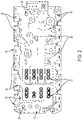
FIG. 2 is an example of a printed circuit board in accordance with the present invention. -
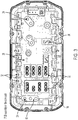
FIG. 3 is an example of a top view of a battery pack in accordance with the present invention with a top housing removed. -
FIG. 4 is an isometric view of the battery pack ofFIG. 3 . -
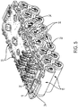
FIG. 5 is an isometric view of the printed circuit board and a plurality of battery cells of the present invention. - Referring to
FIG. 1 , in an example embodiment, abattery pack 10 includes anupper housing 12 and alower housing 14 coupled to theupper housing 12. Thebattery pack 10 includes a plurality ofbattery cells 15 and abattery cell holder 17 holding the plurality ofbattery cells 15. Thebattery pack 10 includes a mechanical interface for coupling to an associated electrical device (not shown), for example a power tool or a battery charger. The interface includes a plurality of slots for providing access to a plurality of battery pack terminals 22 (described in more detail below). The slots allow for ingress of moisture and debris. - Referring to
FIG. 2 , there is illustrated an example of a printedcircuit board 18 in accordance with the present invention. The printedcircuit board 18 may include a plurality of electronic components, such as processors, resistors and capacitors (not shown) that are susceptible to damage if contacted by moisture or debris. As such, it is desirable to encapsulate and enclose these components withLPM material 20. There are other components or features on the printedcircuit board 18, such asbattery pack terminals 22,test points 24, andbattery strap holes 26, that must be accessible to couple or mate with other components. As such, these components and features cannot be encapsulated withLPM material 20. This results in boundaries of theLPM material 20 between components that are encapsulated and components/features that are not encapsulated. - As noted above, the
LPM material 20 does not adhere well to the printedcircuit board 18 exposededges 28 or flat surfaces. To address this shortcoming, the printedcircuit board 18 includes a plurality or array ofadhesion holes 30. Theadhesion holes 30 are positioned at the boundaries of theLPM material 20. Theadhesion holes 30 enable theLPM material 20 to flow through the printedcircuit board 18. As a result, theLPM material 20 wraps around the printedcircuit board 18 providing improved adhesion to the printedcircuit board 18. - As illustrated in
FIG. 2 , theadhesion holes 30 are positioned, for example, around a plurality ofbattery strap holes 26. Each of the plurality ofbattery strap holes 26 receive an end of abattery strap 32. Theadhesion holes 30 are also positioned, for example, around the plurality ofbattery pack terminals 22. Theadhesion holes 30 are also positioned, for example, around the plurality oftest points 24 and thefuses 34. -
FIGs. 3 ,4 and5 illustrate theLPM material 20 applied to theprinted circuit board 18. As illustrated, theLPM material 20 surrounds but does not encapsulate, for example, the battery strap holes 26 and the ends of the battery straps 32 that extend through the battery strap holes 26 or thebattery pack terminals 22 or thefuses 34 or the test points 24. The adhesion holes 30 are positioned along the boundary or border of theLPM material 20 around the various exposed components. The positioning (positions) of the adhesion holes 30 enables theLPM material 20 to flow through the printedcircuit board 18 at the boundary of theLPM material 20. This enables theLPM material 20 to grab or adhere to the printedcircuit board 18. The improved adhesion of theLPM material 20 to the printedcircuit board 18 prevents water and other debris from penetrating or infiltrating between theLPM material 20 and the printedcircuit board 18. This prevents the water or other debris from contaminating any components encapsulated by theLPM material 20. - The plurality of adhesion holes 30 in the printed
circuit board 18 allowLPM material 20 to pass from a first side of the printedcircuit board 18 to a second side of the printedcircuit board 18. In other words, the LMP material is able to wrap or grab the printedcircuit board 18 for improved adhesion. Providing an array of periodic adhesion holes 30 along the boundaries or edges of theLPM material 20 improves adhesion of theLPM material 20 to printedcircuit board 18. - In one embodiment, the adhesion holes 30 have a diameter in the range of approximately 0.5 mm to approximately 2 mm. In another embodiment, the adhesion holes 30 have a diameter of approximately 1 mm. In one embodiment, the distance between edges of adjacent adhesion holes 30 is in a range of approximately 1 mm to approximately 3 mm. In another embodiment, the distance between adjacent edges of adjacent adhesion holes 30 is approximately 2 mm.
- Numerous modifications may be made to the exemplary implementations described above. These and other implementations are within the scope of this application.
Claims (7)
- A battery pack comprising:a housing;a plurality of battery cells;a battery cell holder holding the plurality of battery cells;a printed circuit board;a plurality of components requiring exposure, the plurality of components being affixed to the printed circuit board;a plurality of adhesion holes positioned to form a boundary about the plurality of components; anda low pressure molded material applied to the printed circuit board such that the plurality of components are exposed and surrounded by the low pressure molded material,wherein the low pressure molded material having flowed through the plurality of adhesion holes.
- The battery pack, as recited in claim 1, wherein at least a portion of a boundary of the low pressure molded material is aligned with a subset of the plurality of adhesion holes.
- The battery pack, as recited in claim 1 or 2, wherein the adhesion holes have a diameter in a range of approximately 0.5 mm to approximately 2 mm.
- The battery pack, as recited in claim 1, 2 or 3, wherein the adhesion holes have a diameter of approximately 1 mm.
- The battery pack, as recited in any preceding claim, wherein the distance between adjacent edges of adjacent adhesion holes is approximately 2 mm.
- A battery pack comprising:a housing;a plurality of battery cells;a battery holder holding the plurality of battery cells;a printed circuit board coupled to the battery holder;a plurality of elements associated with the printed circuit board;a plurality of adhesion holes positioned at least partially about the plurality of elements; anda low pressure molded material applied to the printed circuit board such that the plurality of elements are exposed and the low pressure molded material flows through the plurality of adhesion holes.
- The battery pack, as recited in claim 6, wherein a subset of the plurality of adhesion holes are positioned along a portion of a boundary of the low pressure molded material.
Applications Claiming Priority (1)
| Application Number | Priority Date | Filing Date | Title |
|---|---|---|---|
| US202062966623P | 2020-01-28 | 2020-01-28 |
Publications (1)
| Publication Number | Publication Date |
|---|---|
| EP3859869A1 true EP3859869A1 (en) | 2021-08-04 |
Family
ID=74285357
Family Applications (1)
| Application Number | Title | Priority Date | Filing Date |
|---|---|---|---|
| EP21153674.3A Pending EP3859869A1 (en) | 2020-01-28 | 2021-01-27 | Battery pack |
Country Status (1)
| Country | Link |
|---|---|
| EP (1) | EP3859869A1 (en) |
Citations (4)
| Publication number | Priority date | Publication date | Assignee | Title |
|---|---|---|---|---|
| US20100221584A1 (en) * | 2009-02-27 | 2010-09-02 | Andreas Stihl Ag & Co. Kg | Battery Pack with Electronic Monitoring Device Integrated in the Housing Cover |
| JP2011049377A (en) * | 2009-08-27 | 2011-03-10 | Autonetworks Technologies Ltd | Circuit structure, and electrical connection box |
| US20170365826A1 (en) * | 2016-06-20 | 2017-12-21 | Black & Decker Inc. | Battery packs and methods for manufacturing battery packs |
| WO2019163549A1 (en) * | 2018-02-22 | 2019-08-29 | 三洋電機株式会社 | Battery pack and method for producing same |
-
2021
- 2021-01-27 EP EP21153674.3A patent/EP3859869A1/en active Pending
Patent Citations (4)
| Publication number | Priority date | Publication date | Assignee | Title |
|---|---|---|---|---|
| US20100221584A1 (en) * | 2009-02-27 | 2010-09-02 | Andreas Stihl Ag & Co. Kg | Battery Pack with Electronic Monitoring Device Integrated in the Housing Cover |
| JP2011049377A (en) * | 2009-08-27 | 2011-03-10 | Autonetworks Technologies Ltd | Circuit structure, and electrical connection box |
| US20170365826A1 (en) * | 2016-06-20 | 2017-12-21 | Black & Decker Inc. | Battery packs and methods for manufacturing battery packs |
| WO2019163549A1 (en) * | 2018-02-22 | 2019-08-29 | 三洋電機株式会社 | Battery pack and method for producing same |
Similar Documents
| Publication | Publication Date | Title |
|---|---|---|
| US11923557B2 (en) | Battery pack | |
| US12095046B2 (en) | Battery pack and method of manufacture | |
| US6358772B2 (en) | Semiconductor package having semiconductor element mounting structure of semiconductor package mounted on circuit board and method of assembling semiconductor package | |
| US4371912A (en) | Method of mounting interrelated components | |
| US7273769B1 (en) | Method and apparatus for removing encapsulating material from a packaged microelectronic device | |
| EP2169757B1 (en) | Protection circuit module and secondary battery including the protection circuit module | |
| US7433197B2 (en) | Electronic module and method for sealing an electronic module | |
| US8966749B2 (en) | Manufacturing method for protection circuit module of secondary battery | |
| CN112218444B (en) | Battery protection circuit package and manufacturing method thereof | |
| US5726859A (en) | Circuit board component retainer and extractor | |
| CN113659185B (en) | Method for manufacturing battery protection circuit package | |
| US6329594B1 (en) | Integrated circuit package | |
| EP3859869A1 (en) | Battery pack | |
| US6191955B1 (en) | Encapsulation and enclosure of electronic modules | |
| EP3822997A1 (en) | Busbar laminate, electronic component mounting module including same, and method of manufacturing busbar laminate | |
| JP4086123B2 (en) | Semiconductor device | |
| EP0907307A1 (en) | Heat sink for surface mount power packages | |
| US9590227B2 (en) | Protection apparatus of battery pack, method of manufacturing the protection apparatus, and battery pack including the protection apparatus | |
| KR100724179B1 (en) | Data carriers and devices with them | |
| KR102813678B1 (en) | Fixing module of circuit-board and terminal | |
| JP2006344643A (en) | Pack battery | |
| US12322820B2 (en) | Assembly for protecting an SMD component from environmental influences | |
| US8424199B1 (en) | Semiconductor chip mounting system | |
| KR100200289B1 (en) | Self-positioning ic package and wiring board | |
| US8305768B2 (en) | Secondary battery protecting module and lead mounting method |
Legal Events
| Date | Code | Title | Description |
|---|---|---|---|
| PUAI | Public reference made under article 153(3) epc to a published international application that has entered the european phase |
Free format text: ORIGINAL CODE: 0009012 |
|
| STAA | Information on the status of an ep patent application or granted ep patent |
Free format text: STATUS: THE APPLICATION HAS BEEN PUBLISHED |
|
| AK | Designated contracting states |
Kind code of ref document: A1 Designated state(s): AL AT BE BG CH CY CZ DE DK EE ES FI FR GB GR HR HU IE IS IT LI LT LU LV MC MK MT NL NO PL PT RO RS SE SI SK SM TR |
|
| STAA | Information on the status of an ep patent application or granted ep patent |
Free format text: STATUS: REQUEST FOR EXAMINATION WAS MADE |
|
| 17P | Request for examination filed |
Effective date: 20220202 |
|
| RBV | Designated contracting states (corrected) |
Designated state(s): AL AT BE BG CH CY CZ DE DK EE ES FI FR GB GR HR HU IE IS IT LI LT LU LV MC MK MT NL NO PL PT RO RS SE SI SK SM TR |