EP3859760A1 - Method and conductor structure for manufacturing an electric winding of an electromagnetic induction apparatus - Google Patents
Method and conductor structure for manufacturing an electric winding of an electromagnetic induction apparatus Download PDFInfo
- Publication number
- EP3859760A1 EP3859760A1 EP20154715.5A EP20154715A EP3859760A1 EP 3859760 A1 EP3859760 A1 EP 3859760A1 EP 20154715 A EP20154715 A EP 20154715A EP 3859760 A1 EP3859760 A1 EP 3859760A1
- Authority
- EP
- European Patent Office
- Prior art keywords
- supporting structure
- spacer
- spacer elements
- electric winding
- conductor
- Prior art date
- Legal status (The legal status is an assumption and is not a legal conclusion. Google has not performed a legal analysis and makes no representation as to the accuracy of the status listed.)
- Granted
Links
Images




Classifications
-
- H—ELECTRICITY
- H01—ELECTRIC ELEMENTS
- H01F—MAGNETS; INDUCTANCES; TRANSFORMERS; SELECTION OF MATERIALS FOR THEIR MAGNETIC PROPERTIES
- H01F27/00—Details of transformers or inductances, in general
- H01F27/28—Coils; Windings; Conductive connections
- H01F27/32—Insulating of coils, windings, or parts thereof
- H01F27/322—Insulating of coils, windings, or parts thereof the insulation forming channels for circulation of the fluid
-
- H—ELECTRICITY
- H01—ELECTRIC ELEMENTS
- H01F—MAGNETS; INDUCTANCES; TRANSFORMERS; SELECTION OF MATERIALS FOR THEIR MAGNETIC PROPERTIES
- H01F41/00—Apparatus or processes specially adapted for manufacturing or assembling magnets, inductances or transformers; Apparatus or processes specially adapted for manufacturing materials characterised by their magnetic properties
- H01F41/02—Apparatus or processes specially adapted for manufacturing or assembling magnets, inductances or transformers; Apparatus or processes specially adapted for manufacturing materials characterised by their magnetic properties for manufacturing cores, coils, or magnets
- H01F41/04—Apparatus or processes specially adapted for manufacturing or assembling magnets, inductances or transformers; Apparatus or processes specially adapted for manufacturing materials characterised by their magnetic properties for manufacturing cores, coils, or magnets for manufacturing coils
- H01F41/06—Coil winding
-
- H—ELECTRICITY
- H01—ELECTRIC ELEMENTS
- H01F—MAGNETS; INDUCTANCES; TRANSFORMERS; SELECTION OF MATERIALS FOR THEIR MAGNETIC PROPERTIES
- H01F41/00—Apparatus or processes specially adapted for manufacturing or assembling magnets, inductances or transformers; Apparatus or processes specially adapted for manufacturing materials characterised by their magnetic properties
- H01F41/02—Apparatus or processes specially adapted for manufacturing or assembling magnets, inductances or transformers; Apparatus or processes specially adapted for manufacturing materials characterised by their magnetic properties for manufacturing cores, coils, or magnets
- H01F41/04—Apparatus or processes specially adapted for manufacturing or assembling magnets, inductances or transformers; Apparatus or processes specially adapted for manufacturing materials characterised by their magnetic properties for manufacturing cores, coils, or magnets for manufacturing coils
- H01F41/06—Coil winding
- H01F41/061—Winding flat conductive wires or sheets
-
- H—ELECTRICITY
- H01—ELECTRIC ELEMENTS
- H01F—MAGNETS; INDUCTANCES; TRANSFORMERS; SELECTION OF MATERIALS FOR THEIR MAGNETIC PROPERTIES
- H01F27/00—Details of transformers or inductances, in general
- H01F27/28—Coils; Windings; Conductive connections
-
- H—ELECTRICITY
- H01—ELECTRIC ELEMENTS
- H01F—MAGNETS; INDUCTANCES; TRANSFORMERS; SELECTION OF MATERIALS FOR THEIR MAGNETIC PROPERTIES
- H01F27/00—Details of transformers or inductances, in general
- H01F27/28—Coils; Windings; Conductive connections
- H01F27/2823—Wires
-
- H—ELECTRICITY
- H01—ELECTRIC ELEMENTS
- H01F—MAGNETS; INDUCTANCES; TRANSFORMERS; SELECTION OF MATERIALS FOR THEIR MAGNETIC PROPERTIES
- H01F27/00—Details of transformers or inductances, in general
- H01F27/28—Coils; Windings; Conductive connections
- H01F27/32—Insulating of coils, windings, or parts thereof
- H01F27/323—Insulation between winding turns, between winding layers
-
- H—ELECTRICITY
- H01—ELECTRIC ELEMENTS
- H01F—MAGNETS; INDUCTANCES; TRANSFORMERS; SELECTION OF MATERIALS FOR THEIR MAGNETIC PROPERTIES
- H01F5/00—Coils
- H01F5/06—Insulation of windings
-
- H—ELECTRICITY
- H01—ELECTRIC ELEMENTS
- H01F—MAGNETS; INDUCTANCES; TRANSFORMERS; SELECTION OF MATERIALS FOR THEIR MAGNETIC PROPERTIES
- H01F27/00—Details of transformers or inductances, in general
- H01F27/28—Coils; Windings; Conductive connections
- H01F27/2823—Wires
- H01F2027/2838—Wires using transposed wires
-
- H—ELECTRICITY
- H01—ELECTRIC ELEMENTS
- H01F—MAGNETS; INDUCTANCES; TRANSFORMERS; SELECTION OF MATERIALS FOR THEIR MAGNETIC PROPERTIES
- H01F41/00—Apparatus or processes specially adapted for manufacturing or assembling magnets, inductances or transformers; Apparatus or processes specially adapted for manufacturing materials characterised by their magnetic properties
- H01F41/02—Apparatus or processes specially adapted for manufacturing or assembling magnets, inductances or transformers; Apparatus or processes specially adapted for manufacturing materials characterised by their magnetic properties for manufacturing cores, coils, or magnets
- H01F41/04—Apparatus or processes specially adapted for manufacturing or assembling magnets, inductances or transformers; Apparatus or processes specially adapted for manufacturing materials characterised by their magnetic properties for manufacturing cores, coils, or magnets for manufacturing coils
- H01F41/12—Insulating of windings
- H01F41/122—Insulating between turns or between winding layers
Definitions
- the present invention relates to the field of electromagnetic induction apparatuses for electric power transmission and distribution grids, for example power transformers.
- the present invention relates to a method and a conductor structure for manufacturing an electric winding of an electromagnetic induction apparatus.
- Electric windings of electromagnetic induction apparatuses may be manufactured at industrial level according to various methods.
- a widely used method consists in winding a conductor around a winding direction, so that the electric winding has a plurality of adjacent turns arranged around said winding direction.
- electric windings for electromagnetic induction apparatuses have axial and radial channels to ensure the passage of an electrically insulating medium (e.g. insulating fluid or solid cast resin) among the turns.
- an electrically insulating medium e.g. insulating fluid or solid cast resin
- the axial channels of an electric winding are obtained by arranging insulating blocks oriented in parallel to the winding direction while electrically insulating spacers interposed between adjacent turns of the electric winding and oriented radially with respect to the winding direction are arranged to define the radial channels.
- insulating spacers are inserted manually between each pair of adjacent turns, during the winding process.
- insulating spacers are fixed along a suitable lateral surface of a conductor intended to form the turns of the electric winding.
- the conductor structure so obtained is then wound around a winding direction.
- insulating spacers take position between each pair of adjacent turns of said electric winding.
- State-of-the-art electric windings for electromagnetic induction apparatuses generally perform their functions in a rather satisfying way. However, there are still some critical aspects to deal with.
- this phenomenon is due to the fact that, in operation, an electric winding is subject to huge compressive forces along directions substantially parallel to its winding direction.
- the above-illustrated technical issue may lead to a dangerous unbalancing condition of the overall winding structure, which may cause its collapse in certain operating conditions, e.g. when short-circuit currents flow along the electric winding and this latter is subject to huge mechanical stresses.
- the main aim of the present invention is providing a method and a conductor structure for manufacturing an electric winding of an electromagnetic induction apparatus, which allows the above-mentioned critical aspects to be overcome or mitigated.
- another object of the present invention is providing a method and a conductor structure for manufacturing an electric winding, which allow obtaining an electric winding with a high structural balancing and a high resistance to mechanical stresses.
- Another object of the present invention is providing a method and a conductor structure for manufacturing an electric winding, which are relatively easy and inexpensive to implement at industrial level.
- the method comprises the following steps:
- each turn of said electric winding is formed by a corresponding longitudinal portion of said conductor element.
- said spacer elements are interposed between adjacent turns of said electric winding at opposite sides of said turns, when said electric winding is formed.
- said spacer elements are arranged in such a way to bond with the surface of an adjacent turn, when said electric winding is formed.
- said spacer elements are formed by shaped pads of electrically insulating material.
- said shaped pads of electrically insulating material are glued on said supporting structure.
- said shaped pads of electrically insulating material have a surface, on which a layer of gluing material is deposited.
- said spacer elements are formed by shaped regions of electrically insulating material.
- said shaped regions of electrically insulating material are deposited on said supporting structure.
- each spacer band includes spacer elements arranged on a same supporting surface of said supporting structure.
- each spacer band includes spacer elements arranged on opposite supporting surfaces of said supporting structure.
- each spacer band includes spacer elements arranged in such a way to pass through said supporting structure and protrude from opposite surfaces of said supporting structure.
- each spacer band includes spacer elements made in one piece with said supporting structure.
- each spacer band includes spacer elements randomly arranged on said supporting structure.
- each spacer band includes spacer elements arranged on said supporting structure according to a predefined geometric pattern.
- said spacer bands are fixed to said conductor element by gluing or by means of an electrically insulating enclosure element wound around said conductor element.
- said conductor element is a continuously transposed conductor.
- the present invention relates to a conductor structure for manufacturing an electric winding of an electromagnetic induction apparatus according to the following claim 17.
- the conductor structure according to the invention, comprises:
- each turn of said electric winding is formed by a corresponding longitudinal portion of said conductor element.
- said spacer elements are interposed between adjacent turns of said electric winding at opposite sides of said turns, when said electric winding is formed.
- the present invention relates to an electric winding for an electromagnetic induction apparatus, according to the following claim 18.
- the present invention relates to an electromagnetic induction apparatus for electric power transmission and distribution grids according to the following claim 19.
- said electromagnetic induction apparatus is an electric transformer for electric power transmission and distribution grids.
- the present invention relates to a method for manufacturing an electric winding 100 of an electromagnetic induction apparatus (not shown) for electric power transmission and distribution grids.
- Such an electromagnetic induction apparatus may be an electric transformer for electric power transmission and distribution grids, for example a power transformer or a distribution transformer.
- the manufacturing method comprises a step of providing a conductor structure 1 intended to form the electric winding 100.
- the conductor structure 1 comprises a conductor element 2 extending longitudinally along a main extension direction L ( figure 1 ).
- the conductor element 2 is shaped as an elongated parallelepiped including conductive material.
- the conductor element 2 has a shaped section (e.g. a rectangular or square cross section), opposite first and second lateral surfaces 2A, 2B and opposite third and fourth lateral surfaces 2C, 2D.
- a shaped section e.g. a rectangular or square cross section
- the conductor element 2 is a continuously transposed conductor.
- the conductor element 2 may be manufactured according to the construction shown in figure 1 .
- the conductor element 2 comprises two or more stacks 21, 22 of conductors, which are placed side by side along the extension direction L of said conductor element.
- Stacked conductors 20 have portions alternating between the above-mentioned stacks 21, 22. In this way, portions of stacked conductors 20 alternately occupy every possible cross section position along the whole longitudinal extension of the conductor element 2.
- Stacked conductors 20 may be at least partially covered by electrically insulating material.
- the conductor element 2 may include an insulating separator 23 arranged between the stacks 21, 22 of conductors along the extension direction L of said conductor.
- the conductor element 2 may include an insulating band or mesh (not shown) wound around the stacked conductors 20 to maintain these latter in position during the winding operations. According to other embodiments of the invention, however, the conductor element 2 may have different constructions (which may be of known type).
- it may include a single conductor, a plurality of conductors arranged side by side or a bundle of twisted conductors.
- the conductor element 2 may be formed by one or more conductive bars or by one or more conductive foils or disks.
- the conductor structure 1 include one or more layers of electrically insulating material (not shown) arranged in such a way to externally cover the conductor element 2.
- Such an electrically insulating material may be arranged according to solutions of known type.
- it may be selected in a group of materials comprising: paper, polyester materials, aramid or stabilized-PE materials, fiberglass materials, and the like.
- the conductor structure 1 comprises one or more spacer bands 3 arranged on a same corresponding lateral surface 2A or 2B of the conductor element 2.
- Each spacer band 3 includes a supporting structure 30 made of electrically insulating material and a plurality of spacer elements 31 made of electrically insulating material and arranged on said supporting structure.
- each spacer band 3 is spaced one from another along the supporting structure 30 to delimit suitable empty regions 32 ( figure 3, 4 , 7 ).
- the conductor structure 1 is obtained, it is carried out a step of forming the electric winding 100 by means of said conductor structure.
- the electric winding 100 extends axially along the winding direction DW ( figure 2 ).
- the step of forming the electric winding 100 includes winding the conductor structure 1 around the winding direction DW.
- the step of forming the electric winding 100 may include the step of mechanically connecting separated portions of the conductor structure 1 to form the electric winding 100.
- the electric winding 100 has a plurality of adjacent turns 101 arranged around the winding direction DW ( figure 2 ).
- Each turn 101 is formed by a corresponding longitudinal portion of the conductor element 2 included in the winding structure 1.
- the first and second lateral surfaces 2A, 2B of the conductor element 2 are positioned perpendicular to the winding direction DW and form opposite first and second sides 101A, 101B of each turn 101, which extend radially with respect to said winding direction.
- the third and fourth lateral surfaces 2C, 2D of the conductor element 2 are positioned parallel to the winding direction DW and form third and fourth sides 101C, 101D of each turn 101, which extend parallel and coaxially to said winding direction ( figures 2A, 2B ).
- the spacer elements 31 are interposed between adjacent turns 101 at the first and second sides 101A, 101B of these latter.
- the spacer elements 31 lay on radial planes perpendicular to said the winding direction DW ( figure 2 ).
- the empty regions 32 delimited by the spacer elements 31 form radial channels 104 of the electric winding 100, which ensure the passage of an electrically insulating medium (e.g. insulating fluid or solid cast resin) among adjacent turns 101.
- an electrically insulating medium e.g. insulating fluid or solid cast resin
- An important aspect of the invention consists in that, in the electric winding 100, the spacer elements 31, which are interposed between each pair of adjacent turns 101 and distributed along the sides 101A, 101B of said turns, provide a substantially uniform mechanical support to the turns 101 and ensure a stable structural balancing of the electric winding 100.
- each spacer band 3 is formed by an elongated element of electrically insulating material having a reduced thickness (e.g. some millimeters) and two main opposite supporting surfaces 30A, 30B.
- the supporting structure 30 of each spacer band 3 may be formed by a strip of electrically insulating material.
- the supporting structure 30 of each spacer band 3 may be formed by a molded element of electrically insulating material.
- the supporting structure 30 of each spacer band 3 may be formed by a mesh of electrically insulating material.
- the electrically insulating material used for the supporting structure 30 is selected in a group of materials comprising: paper, plastic materials, fiberglass materials, nylon-based materials.
- the supporting structure 30 has a holed or netting structure to favor the passage of heat during the operation of the electric winding 100.
- the spacer bands 3 have the spacer elements 31 arranged on a same supporting surface 30A of the supporting structure 30.
- the opposite supporting surface 30B of the supporting structure 30 is intended to lay on a lateral surface 2A, 2B of the conductor element 2.
- the spacer bands 3 have the spacer elements 31 arranged on both the opposite supporting surfaces 30A, 30B of the supporting structure 30.
- the spacer bands 3 have the spacer elements 31 passing through the thickness of the supporting structure 30 and protruding from the opposite supporting surfaces 30A, 30B of the supporting structure 30 ( figure 7 ).
- the spacer elements 31 may be arranged on the supporting surfaces 30A and/or 30B of a supporting structure according to any desired layout.
- the spacer bands 3 have the spacer elements 31 arranged in a random manner.
- the spacer bands 3 have the spacer elements 31 arranged according to a predefined geometric pattern.
- the spacer bands 3 are fixed to the conductor element 2 by gluing.
- Each spacer band 3 may be directly fixed to the conductors of the conductor element 2, or on an insulating layer of said conductor element or on an additional insulating band or mesh surrounding said conductor element.
- Glue may be applied to a supporting surface 30B of a supporting structure 30 (opposite to the supporting surface 30A on which the spacer elements are arranged) and/or to the corresponding lateral surfaces 2A, 2B of the conductor element 2 in a known manner, for example by spraying, brushing, dusting, by immersion or by applying a prepreg film activatable by UV radiation or heat.
- Special glues designed to withstand high temperatures e.g. up to 250 °C may be used.
- Gluing the one or more spacer bands 3 allows preventing or reducing possible undesired dislocations of these latter.
- Such dislocations of spacer portions 3A, 3B may occur due tangential forces exerted on the winding turns during the operation of the electromagnetic induction apparatus (this phenomenon is also referred to as "spiraling" of the electric winding) or during manufacturing.
- the spacer bands 3 may be fixed to the conductor element 2 by means of an additional electrically insulating enclosure (e.g. formed by an electrically insulating band or mesh wound around the assembly formed by the conductor element 2 and the one or more spacer tapes 3), for example made of a glass-fiber material or polyester.
- an additional electrically insulating enclosure e.g. formed by an electrically insulating band or mesh wound around the assembly formed by the conductor element 2 and the one or more spacer tapes 3
- a glass-fiber material or polyester for example made of a glass-fiber material or polyester.
- the one or more spacer tapes 3 may be directly fixed on the conductors 20 of the electrical conductor element 2, or on an insulating layer of said conductor or on an insulating tape or mesh surrounding said conductor.
- the spacer elements 31 may have any shape according to the needs. As an example, they may have a circular shape, a polygonal shape or even an irregular shape.
- the selected size and distribution density of the spacer elements 31 on the supporting structure 30 depend on the type of the winding 100 to be manufactured (e.g. on the magnitude of the stress forces to which the winding 100 is subject and/or on its cooling requirements).
- the spacer elements 31 have a relatively small size with respect to the width of the supporting structure 30 on which they are arranged. As an example, they may have a width of 5-10 mm and a height of 2 mm.
- the supporting structure 30 and the spacer elements 31 are separated elements assembled through a suitable manufacturing process.
- the spacer elements 31 are arranged in such a way to bond with the surface of an adjacent turn 101, when the electric winding 100 is formed.
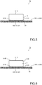
- the spacer elements 31 are formed by shaped pads of electrically insulating material ( figures 5-6 , 8 ).
- such an electrically insulating material is selected in a group of materials comprising: pressed paperboard, plastic materials, fiberglass materials, nylon-based materials.
- the shaped pads 31 of electrically insulating material are glued on the supporting structure 30.
- the shaped pads 31 of electrically insulating material when they are arranged on a supporting surface 30A or 30B of the supporting structure 30, the shaped pads 31 of electrically insulating material have a base surface 31A intended to lay on a supporting surface 30A or 30B of the supporting structure 30 and a top surface 31B, opposite to the base surface 31A ( figures 5-6 ).
- the shaped pads 31 of electrically insulating material are glued on a supporting surface 30A or 30B of the supporting structure 30 at their base surface 31A.
- This can be obtained by depositing a suitable layer 310A of gluing material (e.g. an epoxy resin) on the base surface 31A of each shaped pad 31 and/or on the corresponding region of the supporting surface 30A, 30B on which each shaped 31 is intended to be positioned.
- a suitable layer 310A of gluing material e.g. an epoxy resin
- the shaped pads 31 of electrically insulating material have opposite free surfaces 31A, 31B and a lateral surface at which they are glued with a suitable layer of gluing material 310A with the supporting structure 30 ( figure 8 ).
- the shaped pads 31 comprise at least a surface 31A, 31B on which an additional layer of gluing material 310B (e.g. an epoxy resin) is deposited.
- an additional layer of gluing material 310B e.g. an epoxy resin
- the additional layer of gluing material 310B is conveniently deposited on the top surface 31B of each shaped pad 31 ( figure 6 ).
- the additional layer of gluing material 310B may be conveniently deposited on both the opposite surfaces 31A, 31B of each shaped pad 31 or on one of them only (in this case the surface in distal position with respect to the conductor 2).
- the arrangement of an additional layer on at least a surface of the shaped pads 31 is quite advantageous as it allows obtaining (by means of a suitable thermal treatment) the bonding of each shaped pad 31 to both the adjacent turns 101 between which it is positioned, once the electric winding 100 is formed.
- This solution thus allows further improving the overall structural strength of the electric winding 100.
- this solution is quite effective in preventing or reducing possible undesired dislocations due to the above-mentioned "spiraling" phenomenon.
- the gluing material 310A used for gluing the shaped pads 21 to the supporting structure 30 bonds at ambient temperature.
- the above-mentioned curing temperature (e.g. 100-140°C) is higher than said bonding temperature (e.g. ambient temperature).
- the shaped pads 31 of electrically insulating material may be placed on the supporting structure manually or, preferably, by means of a suitable equipment, which may be of known type.
- the layers of gluing material 310A, 301B may be arranged manually (e.g. by means a suitable tool) or, preferably, by means of suitable industrial equipment, which may be of known type.
- the gluing material 310B used for covering at least a surface 31A, 31B of the shaped pads 31 has a bonding temperature, at which it bonds (e.g. with the surface of adjacent turn 101), and a curing temperature, at which such an electrically insulating material cures.
- the spacer elements 31 are formed by shaped regions of electrically insulating material ( figure 9 ).
- such an electrically insulating material is a gluing material (e.g. an epoxy resin) or, more generally, a suitable plastic material.
- the electrically insulating material used for the shaped regions 31 has a bonding temperature, at which such an electrically insulating material bonds (e.g. with the supporting surface 30A, 30B of the supporting structure 30 and the surface of adjacent turn 101), and a curing temperature, at which such an electrically insulating material cures.
- the above-mentioned curing temperature (e.g. 100-140°C) is higher than said bonding temperature (e.g. ambient temperature).
- the spacer elements 31 are arranged in such a way to bond with the surface of an adjacent turn 101, when the electric winding 100 is formed.
- the shaped regions 31 of electrically insulating material are deposited on a supporting surface 30A, 30B of the supporting structure 30, for example in the form of liquid drops.
- the shaped regions 31 of electrically insulating material may be placed manually (e.g. by means of a suitable tool) or, preferably, by means of suitable industrial equipment, which may be of known type.
- the shaped regions 31 of electrically insulating material may be further subject to a flattening process after the deposition. In this way, the thickness of the shaped regions 31 may be suitably equalized.
- the supporting structure 30 and the spacer elements 31 are made in one piece, e.g. through a moulding process.
- the spacer elements 31 may have comprise at least a surface on which an additional layer of gluing material (e.g. an epoxy resin) is deposited.
- an additional layer of gluing material e.g. an epoxy resin
- the conductor structure 1 comprises a single spacer tape 3 arranged on a same lateral surface 2A, 2B of the conductor element 2 along the entire length of this latter.
- the spacer elements 3 will be continuously distributed on a same lateral surface 2A, 2B along the entire length of the conductor element 2.
- the conductor structure 1 comprises a plurality of spacer bands 3 arranged on a same lateral surface 2A, 2B of the conductor element 2.
- each spacer tape 3 is arranged on at least a lateral surface 2A, 2B of a corresponding longitudinal portion of the conductor element 2, which is intended to form a turn 101 of the electric winding 100 ( figure 11 ).
- the spacer bands 3 are arranged at selected longitudinal portions 2E of the conductor element 2, along the main extension direction L, which are alternate with longitudinal portions 2F, on which no spacer band is present.
- each longitudinal portion 2E, 2F has a length (measured along the main extension direction L) equal to the length of a turn 101 of the electric winding 100.
- the method and conductor structure, according to the invention allow obtaining electric windings with a high structural balancing and a high resistance to mechanical stresses, in particular to compression stresses.
- the method and conductor structure, according to the invention are relatively easy to implement at industrial level at competitive costs with respect to known solutions of the state of the art.
Landscapes
- Engineering & Computer Science (AREA)
- Power Engineering (AREA)
- Manufacturing & Machinery (AREA)
- Insulating Of Coils (AREA)
- Coils Of Transformers For General Uses (AREA)
- Manufacturing Cores, Coils, And Magnets (AREA)
Abstract
Description
- The present invention relates to the field of electromagnetic induction apparatuses for electric power transmission and distribution grids, for example power transformers.
- More particularly, the present invention relates to a method and a conductor structure for manufacturing an electric winding of an electromagnetic induction apparatus.
- Electric windings of electromagnetic induction apparatuses may be manufactured at industrial level according to various methods.
- A widely used method consists in winding a conductor around a winding direction, so that the electric winding has a plurality of adjacent turns arranged around said winding direction.
- As it is known, generally, electric windings for electromagnetic induction apparatuses have axial and radial channels to ensure the passage of an electrically insulating medium (e.g. insulating fluid or solid cast resin) among the turns.
- Traditionally, the axial channels of an electric winding are obtained by arranging insulating blocks oriented in parallel to the winding direction while electrically insulating spacers interposed between adjacent turns of the electric winding and oriented radially with respect to the winding direction are arranged to define the radial channels.
- According to most traditional solutions of the state of the art, the above-mentioned insulating spacers are inserted manually between each pair of adjacent turns, during the winding process. According to more recent manufacturing methods, insulating spacers are fixed along a suitable lateral surface of a conductor intended to form the turns of the electric winding. The conductor structure so obtained is then wound around a winding direction. In this way, insulating spacers take position between each pair of adjacent turns of said electric winding. State-of-the-art electric windings for electromagnetic induction apparatuses generally perform their functions in a rather satisfying way. However, there are still some critical aspects to deal with.
- In operation, electric windings often show deformed turns, particularly at the regions where radial channels are present.
- Basically, this phenomenon is due to the fact that, in operation, an electric winding is subject to huge compressive forces along directions substantially parallel to its winding direction.
- The above-illustrated technical issue may lead to a dangerous unbalancing condition of the overall winding structure, which may cause its collapse in certain operating conditions, e.g. when short-circuit currents flow along the electric winding and this latter is subject to huge mechanical stresses.
- The main aim of the present invention is providing a method and a conductor structure for manufacturing an electric winding of an electromagnetic induction apparatus, which allows the above-mentioned critical aspects to be overcome or mitigated.
- Within this aim, another object of the present invention is providing a method and a conductor structure for manufacturing an electric winding, which allow obtaining an electric winding with a high structural balancing and a high resistance to mechanical stresses. Another object of the present invention is providing a method and a conductor structure for manufacturing an electric winding, which are relatively easy and inexpensive to implement at industrial level. This aim and these objects, together with other objects that will be more apparent from the subsequent description and from the accompanying drawings, are achieved, according to the invention, by a method for manufacturing an electric winding of an electromagnetic induction apparatus, according to
claim 1 and to the related dependent claims. - In a general definition, the method, according to the invention, comprises the following steps:
- providing a conductor structure comprising a conductor element extending longitudinally along a main extension direction and one or more spacer bands arranged on a corresponding lateral surface of said conductor element. Each spacer band includes a supporting structure made of electrically insulating material and spacer elements made of electrically insulating material arranged on said supporting structure. Said spacer elements are spaced one from another, along said supporting structure;
- forming an electric winding by means of said conductor structure. Said electric winding extends axially along a winding direction and it has a plurality of turns arranged around said winding direction.
- According to the invention, each turn of said electric winding is formed by a corresponding longitudinal portion of said conductor element.
- According to the invention, said spacer elements are interposed between adjacent turns of said electric winding at opposite sides of said turns, when said electric winding is formed. According to preferred embodiments of the invention, said spacer elements are arranged in such a way to bond with the surface of an adjacent turn, when said electric winding is formed. According to some embodiments of the invention, said spacer elements are formed by shaped pads of electrically insulating material.
- Preferably, said shaped pads of electrically insulating material are glued on said supporting structure.
- Preferably, said shaped pads of electrically insulating material have a surface, on which a layer of gluing material is deposited.
- According to some embodiments of the invention, said spacer elements are formed by shaped regions of electrically insulating material.
- Preferably, said shaped regions of electrically insulating material are deposited on said supporting structure.
- According to some embodiments of the invention, each spacer band includes spacer elements arranged on a same supporting surface of said supporting structure.
- According to other embodiments of the invention, each spacer band includes spacer elements arranged on opposite supporting surfaces of said supporting structure.
- According to other embodiments of the invention, each spacer band includes spacer elements arranged in such a way to pass through said supporting structure and protrude from opposite surfaces of said supporting structure.
- According to some embodiments of the invention, each spacer band includes spacer elements made in one piece with said supporting structure.
- According to some embodiments of the invention, each spacer band includes spacer elements randomly arranged on said supporting structure.
- According to preferred embodiments of the invention, each spacer band includes spacer elements arranged on said supporting structure according to a predefined geometric pattern. Preferably, said spacer bands are fixed to said conductor element by gluing or by means of an electrically insulating enclosure element wound around said conductor element.
- Preferably, said conductor element is a continuously transposed conductor.
- In a further aspect, the present invention relates to a conductor structure for manufacturing an electric winding of an electromagnetic induction apparatus according to the following claim 17. The conductor structure, according to the invention, comprises:
- a conductor element extending longitudinally along a main extension direction;
- one or more spacer bands arranged on a corresponding lateral surface of said conductor element. Each spacer band includes a supporting structure made of electrically insulating material and spacer elements made of electrically insulating material arranged on said supporting structure. Said spacer elements are spaced one from another, along said supporting structure.
- According to the invention, each turn of said electric winding is formed by a corresponding longitudinal portion of said conductor element.
- According to the invention, said spacer elements are interposed between adjacent turns of said electric winding at opposite sides of said turns, when said electric winding is formed.
- In yet a further aspect, the present invention relates to an electric winding for an electromagnetic induction apparatus, according to the following claim 18.
- In yet a further aspect, the present invention relates to an electromagnetic induction apparatus for electric power transmission and distribution grids according to the following claim 19. Preferably, said electromagnetic induction apparatus is an electric transformer for electric power transmission and distribution grids.
- Further characteristics and advantages of the present invention will be more apparent with reference to the description given below and to the accompanying figures, provided purely for explanatory and non-limiting purposes, wherein:
-
Fig. 1 schematically shows a conductor element used in the manufacturing method and conductor structure, according to the present invention; -
Fig. 2 schematically shows an electric winding for an electromagnetic induction apparatus obtained by means of the manufacturing method, according to the present invention; -
Figs. 2A, 2B schematically show opposite views of a turn portion of the electric winding ofFig. 2 ; -
Figs. 3-4 schematically show a conductor structure, according to some embodiments of the present invention; -
Figs. 5-6 schematically show some details of a spacer band included a conductor structure, according to some embodiments of the present invention; -
Fig. 7 schematically shows a conductor structure, according to another embodiment of the present invention; -
Fig. 8 schematically shows some details of a spacer band included a conductor structure, according to another embodiment of the present invention; -
Fig. 9 schematically shows a conductor structure, according to another embodiment of the present invention. - With reference to the aforesaid figures, the present invention relates to a method for manufacturing an
electric winding 100 of an electromagnetic induction apparatus (not shown) for electric power transmission and distribution grids. - Such an electromagnetic induction apparatus may be an electric transformer for electric power transmission and distribution grids, for example a power transformer or a distribution transformer.
- The manufacturing method, according to the invention, comprises a step of providing a
conductor structure 1 intended to form theelectric winding 100. - The
conductor structure 1 comprises aconductor element 2 extending longitudinally along a main extension direction L (figure 1 ). - Preferably, the
conductor element 2 is shaped as an elongated parallelepiped including conductive material. - Preferably, the
conductor element 2 has a shaped section (e.g. a rectangular or square cross section), opposite first and second lateral surfaces 2A, 2B and opposite third and fourth lateral surfaces 2C, 2D. - According to some embodiments of the invention, the
conductor element 2 is a continuously transposed conductor. - In this case, the
conductor element 2 may be manufactured according to the construction shown infigure 1 . - According to this embodiment of the invention, the
conductor element 2 comprises two ormore stacks -
Stacked conductors 20 have portions alternating between the above-mentionedstacks stacked conductors 20 alternately occupy every possible cross section position along the whole longitudinal extension of theconductor element 2. -
Stacked conductors 20 may be at least partially covered by electrically insulating material. - The
conductor element 2 may include an insulatingseparator 23 arranged between thestacks - The
conductor element 2 may include an insulating band or mesh (not shown) wound around the stackedconductors 20 to maintain these latter in position during the winding operations. According to other embodiments of the invention, however, theconductor element 2 may have different constructions (which may be of known type). - For example, it may include a single conductor, a plurality of conductors arranged side by side or a bundle of twisted conductors.
- As a further example, the
conductor element 2 may be formed by one or more conductive bars or by one or more conductive foils or disks. - According to some embodiments of the invention (not shown), the
conductor structure 1 include one or more layers of electrically insulating material (not shown) arranged in such a way to externally cover theconductor element 2. - Such an electrically insulating material may be arranged according to solutions of known type. For example, it may be selected in a group of materials comprising: paper, polyester materials, aramid or stabilized-PE materials, fiberglass materials, and the like.
- The
conductor structure 1 comprises one ormore spacer bands 3 arranged on a same correspondinglateral surface conductor element 2. - Each
spacer band 3 includes a supportingstructure 30 made of electrically insulating material and a plurality ofspacer elements 31 made of electrically insulating material and arranged on said supporting structure. - Conveniently, the
spacer elements 31 of eachspacer band 3 are spaced one from another along the supportingstructure 30 to delimit suitable empty regions 32 (figure 3, 4 ,7 ). - According to the method of the invention, once the
conductor structure 1 is obtained, it is carried out a step of forming the electric winding 100 by means of said conductor structure. The electric winding 100 extends axially along the winding direction DW (figure 2 ). Preferably, e.g. when the conductor structure can be bent by means of a suitable bending apparatus, the step of forming the electric winding 100 includes winding theconductor structure 1 around the winding direction DW. - According to alternative embodiments, e.g. when the conductor structure cannot be bent, the step of forming the electric winding 100 may include the step of mechanically connecting separated portions of the
conductor structure 1 to form the electric winding 100. - The electric winding 100 has a plurality of
adjacent turns 101 arranged around the winding direction DW (figure 2 ). - Each
turn 101 is formed by a corresponding longitudinal portion of theconductor element 2 included in the windingstructure 1. - In the electric winding 100, the first and second lateral surfaces 2A, 2B of the
conductor element 2 are positioned perpendicular to the winding direction DW and form opposite first andsecond sides turn 101, which extend radially with respect to said winding direction. - On the other hand, the third and fourth lateral surfaces 2C, 2D of the
conductor element 2 are positioned parallel to the winding direction DW and form third andfourth sides turn 101, which extend parallel and coaxially to said winding direction (figures 2A, 2B ). - In the electric winding 1, due to their positioning along the first and
second surfaces conductor element 2, thespacer elements 31 are interposed betweenadjacent turns 101 at the first andsecond sides - In this way, the
spacer elements 31 lay on radial planes perpendicular to said the winding direction DW (figure 2 ). - The
empty regions 32 delimited by thespacer elements 31form radial channels 104 of the electric winding 100, which ensure the passage of an electrically insulating medium (e.g. insulating fluid or solid cast resin) among adjacent turns 101. - An important aspect of the invention consists in that, in the electric winding 100, the
spacer elements 31, which are interposed between each pair ofadjacent turns 101 and distributed along thesides turns 101 and ensure a stable structural balancing of the electric winding 100. - It has been seen that the solution provided by the claimed invention greatly improves the overall resistance of the electric winding 100 to compressive forces as it ensures an optimal structural balancing.
- It is therefore possible to prevent or remarkably mitigate the onset of deformation phenomena of the turns of the electric winding 100 during the operation of the electromagnetic induction apparatus.
- Preferably, the supporting
structure 30 of eachspacer band 3 is formed by an elongated element of electrically insulating material having a reduced thickness (e.g. some millimeters) and two main opposite supportingsurfaces - According to some embodiments of the invention, the supporting
structure 30 of eachspacer band 3 may be formed by a strip of electrically insulating material. - According to other embodiments of the invention, the supporting
structure 30 of eachspacer band 3 may be formed by a molded element of electrically insulating material. - According to yet another embodiment of the invention, the supporting
structure 30 of eachspacer band 3 may be formed by a mesh of electrically insulating material. - Preferably, the electrically insulating material used for the supporting
structure 30 is selected in a group of materials comprising: paper, plastic materials, fiberglass materials, nylon-based materials. - Preferably, the supporting
structure 30 has a holed or netting structure to favor the passage of heat during the operation of the electric winding 100. - According to some embodiments of the invention (
figures 3-4 ), thespacer bands 3 have thespacer elements 31 arranged on a same supportingsurface 30A of the supportingstructure 30. In this case, the opposite supportingsurface 30B of the supportingstructure 30 is intended to lay on alateral surface conductor element 2. - According to other embodiments of the invention (not shown), the
spacer bands 3 have thespacer elements 31 arranged on both the opposite supportingsurfaces structure 30. - According to yet other embodiments of the invention, the
spacer bands 3 have thespacer elements 31 passing through the thickness of the supportingstructure 30 and protruding from the opposite supportingsurfaces figure 7 ). - In principle, the
spacer elements 31 may be arranged on the supportingsurfaces 30A and/or 30B of a supporting structure according to any desired layout. - According to some embodiments of the invention (
figures 3 ,7 ), thespacer bands 3 have thespacer elements 31 arranged in a random manner. - According to other embodiments of the invention (
figure 4 ), thespacer bands 3 have thespacer elements 31 arranged according to a predefined geometric pattern. - According to some embodiments of the invention (in particular where the
spacer elements 31 are arranged on a same supportingsurface 30A of the supporting structure 30), thespacer bands 3 are fixed to theconductor element 2 by gluing. - Each
spacer band 3 may be directly fixed to the conductors of theconductor element 2, or on an insulating layer of said conductor element or on an additional insulating band or mesh surrounding said conductor element. - Glue may be applied to a supporting
surface 30B of a supporting structure 30 (opposite to the supportingsurface 30A on which the spacer elements are arranged) and/or to the correspondinglateral surfaces conductor element 2 in a known manner, for example by spraying, brushing, dusting, by immersion or by applying a prepreg film activatable by UV radiation or heat. - Special glues designed to withstand high temperatures (e.g. up to 250 °C) may be used.
- The above-describe solutions are quite advantageous. Gluing the one or
more spacer bands 3 allows preventing or reducing possible undesired dislocations of these latter. Such dislocations of spacer portions 3A, 3B may occur due tangential forces exerted on the winding turns during the operation of the electromagnetic induction apparatus (this phenomenon is also referred to as "spiraling" of the electric winding) or during manufacturing. - According to other embodiments of the invention (in particular where the
spacer elements 31 are arranged on both the supportingsurfaces structure 30 or pass through it), thespacer bands 3 may be fixed to theconductor element 2 by means of an additional electrically insulating enclosure (e.g. formed by an electrically insulating band or mesh wound around the assembly formed by theconductor element 2 and the one or more spacer tapes 3), for example made of a glass-fiber material or polyester. - Also, in this case, the one or
more spacer tapes 3 may be directly fixed on theconductors 20 of theelectrical conductor element 2, or on an insulating layer of said conductor or on an insulating tape or mesh surrounding said conductor. - In principle, the
spacer elements 31 may have any shape according to the needs. As an example, they may have a circular shape, a polygonal shape or even an irregular shape. - In general, the selected size and distribution density of the
spacer elements 31 on the supportingstructure 30 depend on the type of the winding 100 to be manufactured (e.g. on the magnitude of the stress forces to which the winding 100 is subject and/or on its cooling requirements). - However, preferably, the
spacer elements 31 have a relatively small size with respect to the width of the supportingstructure 30 on which they are arranged. As an example, they may have a width of 5-10 mm and a height of 2 mm. - In general, the supporting
structure 30 and thespacer elements 31 are separated elements assembled through a suitable manufacturing process. - According to preferred embodiments of the invention, the
spacer elements 31 are arranged in such a way to bond with the surface of anadjacent turn 101, when the electric winding 100 is formed. - As it will be better discussed below, this solution is quite effective in preventing or reducing possible undesired dislocations due to the above-mentioned "spiraling" phenomenon. According to some embodiments of the invention, the
spacer elements 31 are formed by shaped pads of electrically insulating material (figures 5-6 ,8 ). - Preferably, such an electrically insulating material is selected in a group of materials comprising: pressed paperboard, plastic materials, fiberglass materials, nylon-based materials. Preferably, the shaped
pads 31 of electrically insulating material are glued on the supportingstructure 30. - Preferably, when they are arranged on a supporting
surface structure 30, the shapedpads 31 of electrically insulating material have abase surface 31A intended to lay on a supportingsurface structure 30 and atop surface 31B, opposite to thebase surface 31A (figures 5-6 ). - Preferably, the shaped
pads 31 of electrically insulating material are glued on a supportingsurface structure 30 at theirbase surface 31A. This can be obtained by depositing asuitable layer 310A of gluing material (e.g. an epoxy resin) on thebase surface 31A of each shapedpad 31 and/or on the corresponding region of the supportingsurface - Preferably, when they pass through the supporting
structure 30, the shapedpads 31 of electrically insulating material have oppositefree surfaces material 310A with the supporting structure 30 (figure 8 ). - Preferably, the shaped
pads 31 comprise at least asurface material 310B (e.g. an epoxy resin) is deposited. - In the embodiment of
figure 5 , the additional layer of gluingmaterial 310B is conveniently deposited on thetop surface 31B of each shaped pad 31 (figure 6 ). - In the embodiment of
figure 8 , the additional layer of gluingmaterial 310B may be conveniently deposited on both theopposite surfaces pad 31 or on one of them only (in this case the surface in distal position with respect to the conductor 2). The arrangement of an additional layer on at least a surface of the shapedpads 31 is quite advantageous as it allows obtaining (by means of a suitable thermal treatment) the bonding of each shapedpad 31 to both the adjacent turns 101 between which it is positioned, once the electric winding 100 is formed. - This solution thus allows further improving the overall structural strength of the electric winding 100. In particular, this solution is quite effective in preventing or reducing possible undesired dislocations due to the above-mentioned "spiraling" phenomenon.
- Preferably, the gluing
material 310A used for gluing the shapedpads 21 to the supportingstructure 30 bonds at ambient temperature. - Preferably, the above-mentioned curing temperature (e.g. 100-140°C) is higher than said bonding temperature (e.g. ambient temperature).
- The shaped
pads 31 of electrically insulating material may be placed on the supporting structure manually or, preferably, by means of a suitable equipment, which may be of known type. - The layers of gluing
material 310A, 301B may be arranged manually (e.g. by means a suitable tool) or, preferably, by means of suitable industrial equipment, which may be of known type. Preferably, the gluingmaterial 310B used for covering at least asurface pads 31 has a bonding temperature, at which it bonds (e.g. with the surface of adjacent turn 101), and a curing temperature, at which such an electrically insulating material cures. According to some embodiments of the invention, thespacer elements 31 are formed by shaped regions of electrically insulating material (figure 9 ). - Preferably, such an electrically insulating material is a gluing material (e.g. an epoxy resin) or, more generally, a suitable plastic material.
- Preferably, the electrically insulating material used for the shaped
regions 31 has a bonding temperature, at which such an electrically insulating material bonds (e.g. with the supportingsurface structure 30 and the surface of adjacent turn 101), and a curing temperature, at which such an electrically insulating material cures. - Preferably, the above-mentioned curing temperature (e.g. 100-140°C) is higher than said bonding temperature (e.g. ambient temperature).
- it is evident that also, according to these embodiment of the invention, the spacer elements 31 (in this case formed by shaped regions of electrically insulating material) are arranged in such a way to bond with the surface of an
adjacent turn 101, when the electric winding 100 is formed. Preferably, the shapedregions 31 of electrically insulating material are deposited on a supportingsurface structure 30, for example in the form of liquid drops. - The shaped
regions 31 of electrically insulating material may be placed manually (e.g. by means of a suitable tool) or, preferably, by means of suitable industrial equipment, which may be of known type. - Since they may have a different thickness when they are deposited on the supporting
structure 30, the shapedregions 31 of electrically insulating material may be further subject to a flattening process after the deposition. In this way, the thickness of the shapedregions 31 may be suitably equalized. - According to other embodiments of the invention (not shown), the supporting
structure 30 and thespacer elements 31 are made in one piece, e.g. through a moulding process. - Also in this case, the
spacer elements 31 may have comprise at least a surface on which an additional layer of gluing material (e.g. an epoxy resin) is deposited. - According to some embodiments of the invention (
figure 10 ), theconductor structure 1 comprises asingle spacer tape 3 arranged on a samelateral surface conductor element 2 along the entire length of this latter. In this case, thespacer elements 3 will be continuously distributed on a samelateral surface conductor element 2. - According to some embodiments of the invention, the
conductor structure 1 comprises a plurality ofspacer bands 3 arranged on a samelateral surface conductor element 2. - Preferably, each
spacer tape 3 is arranged on at least alateral surface conductor element 2, which is intended to form aturn 101 of the electric winding 100 (figure 11 ). - Preferably, the
spacer bands 3 are arranged at selectedlongitudinal portions 2E of theconductor element 2, along the main extension direction L, which are alternate withlongitudinal portions 2F, on which no spacer band is present. - Conveniently, each
longitudinal portion turn 101 of the electric winding 100. - The method and the conductor structure, according to the invention, provide relevant advantages.
- The method and conductor structure, according to the invention, allow obtaining electric windings with a high structural balancing and a high resistance to mechanical stresses, in particular to compression stresses.
- This allows preventing or reducing the deformation of the turns of the electric winding in operation with a consequent remarkable increase of the reliability of the electromagnetic induction apparatus in operation, even in presence of fault events or short-circuit events.
- The method and conductor structure, according to the invention, are relatively easy to implement at industrial level at competitive costs with respect to known solutions of the state of the art.
Claims (19)
- A method for manufacturing an electric winding (100) of an electromagnetic induction apparatus, characterised in that it comprises the following steps:- providing a conductor structure (1) comprising a conductor element (2) extending longitudinally along a main extension direction (L) and one or more spacer bands (3) arranged on a corresponding lateral surface of said conductor element, each spacer band including a supporting structure (30) made of electrically insulating material and spacer elements (31) made of electrically insulating material arranged on said supporting structure, said spacer elements being spaced one from another, along said supporting structure;- forming an electric winding (100) by means of said conductor structure, said electric winding extending axially along a winding direction (DW) and having a plurality of turns (101) arranged around said winding direction;
wherein each turn (101) of said electric winding (100) is formed by a corresponding longitudinal portion (2E, 2F) of said conductor element (2);
wherein said spacer elements (31) are interposed between adjacent turns of said electric winding (100) at opposite sides (101A, 101B) of said turns (101). - Method, according to claim 1, characterised in that said spacer elements (31) bond with an adjacent turn, when said electric winding (100) is formed.
- Method, according to claim 1 or 2, characterised in that said spacer elements (31) are formed by shaped pads of electrically insulating material.
- Method, according to claim 3, characterised in that said shaped pads (31) of electrically insulating material are glued to said supporting structure (30).
- Method, according to one of the claims from 2 to 4, characterised in that said shaped pads (31) of electrically insulating material have a surface (31B), on which a layer (310B) of gluing material is deposited.
- Method, according to claim 1, characterised in that said spacer elements (31) are formed by shaped regions of electrically insulating material.
- Method, according to claim 6, characterised in that said shaped regions (31) of electrically insulating material are deposited on said supporting structure (30).
- Method, according to one of the previous claims, characterised in that each spacer band (3) includes spacer elements (31) arranged on a same supporting surface (30A) of said supporting structure (30).
- Method, according to one of the previous claims, characterised in that each spacer band (3) includes spacer elements (31) arranged on opposite supporting surfaces (30A, 30B) of said supporting structure (30).
- Method, according to one of the claims from 1 to 8, characterised in that each spacer band (3) includes spacer elements (31) arranged in such a way to pass through said supporting structure (3) and protrude from opposite surfaces (30A, 30B) of said supporting structure (30).
- Method, according to one of the claims from 8 to 10, characterised in that each spacer band (3) includes spacer elements (31) made in one piece with said supporting structure (3).
- Method, according to one of the previous claims, characterised in that each spacer band (3) includes spacer elements (31) randomly arranged on said supporting structure (30).
- Method, according to one of the claims from 1 to 11, characterised in that each spacer band (3) includes spacer elements (31) arranged on said supporting structure (30) according to a predefined geometric pattern.
- Method, according to one of the previous claims, characterised in that said spacer bands (3) are fixed to said conductor element (2) by gluing or by means of an electrically insulating enclosure element wound around said conductor element.
- Method, according to one or more of the previous claims, characterised in that said conductor element (2) is a continuously transposed conductor.
- Method, according to one or more of the previous claims, characterised in that said electromagnetic induction apparatus is an electric transformer for electric power transmission and distribution grids.
- A conductor structure (1) for manufacturing an electric winding (100) of an electromagnetic induction apparatus, comprising:- a conductor element (2) extending longitudinally along a main extension direction (L);- one or more spacer bands (3) arranged on a corresponding lateral surface of said conductor element, each spacer band including a supporting structure (30) made of electrically insulating material and spacer elements (31) made of electrically insulating material arranged on said supporting structure, said spacer elements being spaced one from another along said supporting structure;
wherein said conductor structure (1) is intended to form an electric winding (100) extending axially along said winding direction and having a plurality of turns (101) arranged around said electric winding direction,
wherein each turn (101) of said electric winding (100) is formed by a corresponding longitudinal portion (2E, 2F) of said conductor element (2);
wherein said spacer elements (31) are interposed between adjacent turns of said electric winding (100) at opposite sides (101A, 101B) of said turns (101). - An electric winding (100) for an electromagnetic induction apparatus characterised in that it comprises a conductor structure (1), according to claim 17.
- An electromagnetic induction apparatus for electric power transmission and distribution grids characterised in that it includes an electric winding (100), according to claim 18.
Priority Applications (7)
| Application Number | Priority Date | Filing Date | Title |
|---|---|---|---|
| EP20154715.5A EP3859760B1 (en) | 2020-01-30 | 2020-01-30 | Method and conductor structure for manufacturing an electric winding of an electromagnetic induction apparatus |
| CA3142458A CA3142458C (en) | 2020-01-30 | 2020-12-28 | Method and conductor structure for manufacturing an electric winding of an electromagnetic induction apparatus |
| PCT/EP2020/087937 WO2021151610A1 (en) | 2020-01-30 | 2020-12-28 | Method and conductor structure for manufacturing an electric winding of an electromagnetic induction apparatus |
| US17/631,521 US11657961B2 (en) | 2020-01-30 | 2020-12-28 | Method and conductor structure for manufacturing an electric winding of an electromagnetic induction apparatus |
| JP2022505354A JP7196362B2 (en) | 2020-01-30 | 2020-12-28 | Method and conductor structure for manufacturing electrical windings for electromagnetic induction devices |
| CN202080054184.3A CN114175192A (en) | 2020-01-30 | 2020-12-28 | Method and conductor structure for producing an electrical winding of an electromagnetic induction device |
| KR1020227001552A KR102411469B1 (en) | 2020-01-30 | 2020-12-28 | Method and conductor structure for manufacturing electrical windings of electromagnetic induction devices |
Applications Claiming Priority (1)
| Application Number | Priority Date | Filing Date | Title |
|---|---|---|---|
| EP20154715.5A EP3859760B1 (en) | 2020-01-30 | 2020-01-30 | Method and conductor structure for manufacturing an electric winding of an electromagnetic induction apparatus |
Publications (2)
| Publication Number | Publication Date |
|---|---|
| EP3859760A1 true EP3859760A1 (en) | 2021-08-04 |
| EP3859760B1 EP3859760B1 (en) | 2024-06-19 |
Family
ID=69411391
Family Applications (1)
| Application Number | Title | Priority Date | Filing Date |
|---|---|---|---|
| EP20154715.5A Active EP3859760B1 (en) | 2020-01-30 | 2020-01-30 | Method and conductor structure for manufacturing an electric winding of an electromagnetic induction apparatus |
Country Status (7)
| Country | Link |
|---|---|
| US (1) | US11657961B2 (en) |
| EP (1) | EP3859760B1 (en) |
| JP (1) | JP7196362B2 (en) |
| KR (1) | KR102411469B1 (en) |
| CN (1) | CN114175192A (en) |
| CA (1) | CA3142458C (en) |
| WO (1) | WO2021151610A1 (en) |
Families Citing this family (1)
| Publication number | Priority date | Publication date | Assignee | Title |
|---|---|---|---|---|
| EP4026879A1 (en) * | 2021-01-11 | 2022-07-13 | Hitachi Energy Switzerland AG | Spacer tape, method for manufacturing a winding and winding |
Citations (3)
| Publication number | Priority date | Publication date | Assignee | Title |
|---|---|---|---|---|
| DE2653315A1 (en) * | 1976-10-29 | 1978-05-03 | Bbc Brown Boveri & Cie | INSULATION AND DISTANCE BODY FOR AXIAL INSULATION AND DISTANCING OF THE CONDUCTORS FROM COILS AND THE PROCESS FOR THE PRODUCTION THEREOF |
| CN209496640U (en) * | 2019-04-11 | 2019-10-15 | 陕西兰威机电有限责任公司 | Band oil duct transposed conductor |
| WO2019238558A1 (en) * | 2018-06-12 | 2019-12-19 | Asta Elektrodraht Gmbh | Multiple parallel conductor with spacer plates |
Family Cites Families (13)
| Publication number | Priority date | Publication date | Assignee | Title |
|---|---|---|---|---|
| GB1242401A (en) * | 1967-11-07 | 1971-08-11 | Bruce Peebles Ind Ltd | Transformer or reactor winding |
| DE2812466A1 (en) | 1978-03-22 | 1979-09-27 | Authenrieth Presspanfab | INSULATING MATERIAL FOR HIGH VOLTAGE DEVICES OR DGL. |
| SE421570B (en) | 1980-05-21 | 1982-01-04 | Asea Ab | WITH ISOLERATED COOL BAND WINDING FOR A TRANSFORMER OR REACTOR |
| IT1218980B (en) * | 1988-01-27 | 1990-04-24 | Marelli Autronica | ELECTRIC INCLINATION SENSOR AND DETECTION CIRCUIT FOR SUCH SENSOR |
| JPH0385708A (en) | 1989-08-30 | 1991-04-10 | Hitachi Ltd | Construction of winding for transformer |
| AT399962B (en) | 1992-09-16 | 1995-08-25 | Asta Eisen Und Metallwarenerze | THIRD PARTY |
| JP2002118020A (en) | 2000-10-10 | 2002-04-19 | Fuji Electric Co Ltd | Dislocation conductor and induction winding |
| EP2853313B1 (en) * | 2013-09-26 | 2017-09-20 | ABB Schweiz AG | Method of manufacturing a polymer-insulated conductor |
| JP7178558B2 (en) * | 2017-04-13 | 2022-11-28 | パナソニックIpマネジメント株式会社 | Coil and motor using it |
| DE102017208814A1 (en) * | 2017-05-24 | 2018-11-29 | Isotek Gmbh | Spacer tape, transformer winding and transformer and the method for producing a spacer strip |
| JP2019192785A (en) | 2018-04-25 | 2019-10-31 | 三菱電機株式会社 | Mold coil, mold coil manufacturing apparatus, and manufacturing method of the mold coil |
| IT201800002572U1 (en) | 2018-05-17 | 2019-11-17 | Transposed cable and winding made by means of said transposed cable | |
| EP3839987B1 (en) * | 2019-12-18 | 2024-04-17 | Hitachi Energy Ltd | Method and conductor structure for manufacturing an electric winding of an electromagnetic induction apparatus |
-
2020
- 2020-01-30 EP EP20154715.5A patent/EP3859760B1/en active Active
- 2020-12-28 CN CN202080054184.3A patent/CN114175192A/en active Pending
- 2020-12-28 CA CA3142458A patent/CA3142458C/en active Active
- 2020-12-28 KR KR1020227001552A patent/KR102411469B1/en active Active
- 2020-12-28 US US17/631,521 patent/US11657961B2/en active Active
- 2020-12-28 WO PCT/EP2020/087937 patent/WO2021151610A1/en not_active Ceased
- 2020-12-28 JP JP2022505354A patent/JP7196362B2/en active Active
Patent Citations (3)
| Publication number | Priority date | Publication date | Assignee | Title |
|---|---|---|---|---|
| DE2653315A1 (en) * | 1976-10-29 | 1978-05-03 | Bbc Brown Boveri & Cie | INSULATION AND DISTANCE BODY FOR AXIAL INSULATION AND DISTANCING OF THE CONDUCTORS FROM COILS AND THE PROCESS FOR THE PRODUCTION THEREOF |
| WO2019238558A1 (en) * | 2018-06-12 | 2019-12-19 | Asta Elektrodraht Gmbh | Multiple parallel conductor with spacer plates |
| CN209496640U (en) * | 2019-04-11 | 2019-10-15 | 陕西兰威机电有限责任公司 | Band oil duct transposed conductor |
Also Published As
| Publication number | Publication date |
|---|---|
| US20220270809A1 (en) | 2022-08-25 |
| KR102411469B1 (en) | 2022-06-22 |
| KR20220011227A (en) | 2022-01-27 |
| EP3859760B1 (en) | 2024-06-19 |
| JP2022535620A (en) | 2022-08-09 |
| CA3142458A1 (en) | 2021-08-05 |
| CN114175192A (en) | 2022-03-11 |
| JP7196362B2 (en) | 2022-12-26 |
| US11657961B2 (en) | 2023-05-23 |
| CA3142458C (en) | 2023-03-28 |
| WO2021151610A1 (en) | 2021-08-05 |
Similar Documents
| Publication | Publication Date | Title |
|---|---|---|
| US4538131A (en) | Air-core choke coil | |
| US20100162557A1 (en) | Method of forming a disc-wound transformer with improved cooling and impulse voltage distribution | |
| KR20120094014A (en) | Continuously transposed conductor | |
| EP2320440B1 (en) | Transformer winding and a method of reinforcing a transformer winding | |
| CN112534525B (en) | Multiple parallel conductors with spacer plates | |
| CA3142458C (en) | Method and conductor structure for manufacturing an electric winding of an electromagnetic induction apparatus | |
| EP2963662B1 (en) | Oil-filled transformer | |
| EP3839987B1 (en) | Method and conductor structure for manufacturing an electric winding of an electromagnetic induction apparatus | |
| US20090174518A1 (en) | Toroidal star-shaped transformer | |
| JP2004047482A (en) | Induction heating device | |
| CA1177546A (en) | Inductor and process of manufacturing the same | |
| JP4295744B2 (en) | Round wire, coil, stator coil, rotor coil, and transformer | |
| KR102742985B1 (en) | Method for manufacturing electric winding of electromagnetic induction device and conductor structure | |
| EP4086927B1 (en) | Coil for a transformer core | |
| JP6255697B2 (en) | Resin molded coil, manufacturing method thereof, and molded transformer | |
| JP2003151754A5 (en) | ||
| JP4845239B2 (en) | Induction heating coil | |
| WO2014207155A1 (en) | Method for producing a coil device, an end ring element and a coil device having an end ring element | |
| KR102905535B1 (en) | a method for manufacturing of transformer which multi layer type | |
| JP2002118020A (en) | Dislocation conductor and induction winding | |
| KR20120098302A (en) | Environment-friendly power supply for the pole transformer | |
| JPH1187147A (en) | Winding of electromagnetic induction equipment | |
| CN120089518A (en) | Coil assembly manufacturing method, voltage transformer production method and voltage transformer | |
| JPH0719692B2 (en) | Superconducting coil | |
| JPS58150206A (en) | Transposed wire for induction electric appliances |
Legal Events
| Date | Code | Title | Description |
|---|---|---|---|
| PUAI | Public reference made under article 153(3) epc to a published international application that has entered the european phase |
Free format text: ORIGINAL CODE: 0009012 |
|
| STAA | Information on the status of an ep patent application or granted ep patent |
Free format text: STATUS: THE APPLICATION HAS BEEN PUBLISHED |
|
| AK | Designated contracting states |
Kind code of ref document: A1 Designated state(s): AL AT BE BG CH CY CZ DE DK EE ES FI FR GB GR HR HU IE IS IT LI LT LU LV MC MK MT NL NO PL PT RO RS SE SI SK SM TR |
|
| STAA | Information on the status of an ep patent application or granted ep patent |
Free format text: STATUS: REQUEST FOR EXAMINATION WAS MADE |
|
| RAP3 | Party data changed (applicant data changed or rights of an application transferred) |
Owner name: HITACHI ENERGY SWITZERLAND AG |
|
| 17P | Request for examination filed |
Effective date: 20211228 |
|
| RBV | Designated contracting states (corrected) |
Designated state(s): AL AT BE BG CH CY CZ DE DK EE ES FI FR GB GR HR HU IE IS IT LI LT LU LV MC MK MT NL NO PL PT RO RS SE SI SK SM TR |
|
| P01 | Opt-out of the competence of the unified patent court (upc) registered |
Effective date: 20230527 |
|
| RAP1 | Party data changed (applicant data changed or rights of an application transferred) |
Owner name: HITACHI ENERGY LTD |
|
| GRAP | Despatch of communication of intention to grant a patent |
Free format text: ORIGINAL CODE: EPIDOSNIGR1 |
|
| STAA | Information on the status of an ep patent application or granted ep patent |
Free format text: STATUS: GRANT OF PATENT IS INTENDED |
|
| INTG | Intention to grant announced |
Effective date: 20240209 |
|
| GRAS | Grant fee paid |
Free format text: ORIGINAL CODE: EPIDOSNIGR3 |
|
| GRAA | (expected) grant |
Free format text: ORIGINAL CODE: 0009210 |
|
| STAA | Information on the status of an ep patent application or granted ep patent |
Free format text: STATUS: THE PATENT HAS BEEN GRANTED |
|
| AK | Designated contracting states |
Kind code of ref document: B1 Designated state(s): AL AT BE BG CH CY CZ DE DK EE ES FI FR GB GR HR HU IE IS IT LI LT LU LV MC MK MT NL NO PL PT RO RS SE SI SK SM TR |
|
| REG | Reference to a national code |
Ref country code: GB Ref legal event code: FG4D |
|
| REG | Reference to a national code |
Ref country code: CH Ref legal event code: EP |
|
| REG | Reference to a national code |
Ref country code: DE Ref legal event code: R096 Ref document number: 602020032518 Country of ref document: DE |
|
| PG25 | Lapsed in a contracting state [announced via postgrant information from national office to epo] |
Ref country code: BG Free format text: LAPSE BECAUSE OF FAILURE TO SUBMIT A TRANSLATION OF THE DESCRIPTION OR TO PAY THE FEE WITHIN THE PRESCRIBED TIME-LIMIT Effective date: 20240619 |
|
| PG25 | Lapsed in a contracting state [announced via postgrant information from national office to epo] |
Ref country code: HR Free format text: LAPSE BECAUSE OF FAILURE TO SUBMIT A TRANSLATION OF THE DESCRIPTION OR TO PAY THE FEE WITHIN THE PRESCRIBED TIME-LIMIT Effective date: 20240619 Ref country code: FI Free format text: LAPSE BECAUSE OF FAILURE TO SUBMIT A TRANSLATION OF THE DESCRIPTION OR TO PAY THE FEE WITHIN THE PRESCRIBED TIME-LIMIT Effective date: 20240619 |
|
| REG | Reference to a national code |
Ref country code: LT Ref legal event code: MG9D |
|
| PG25 | Lapsed in a contracting state [announced via postgrant information from national office to epo] |
Ref country code: GR Free format text: LAPSE BECAUSE OF FAILURE TO SUBMIT A TRANSLATION OF THE DESCRIPTION OR TO PAY THE FEE WITHIN THE PRESCRIBED TIME-LIMIT Effective date: 20240920 |
|
| REG | Reference to a national code |
Ref country code: NL Ref legal event code: MP Effective date: 20240619 |
|
| PG25 | Lapsed in a contracting state [announced via postgrant information from national office to epo] |
Ref country code: LV Free format text: LAPSE BECAUSE OF FAILURE TO SUBMIT A TRANSLATION OF THE DESCRIPTION OR TO PAY THE FEE WITHIN THE PRESCRIBED TIME-LIMIT Effective date: 20240619 |
|
| PG25 | Lapsed in a contracting state [announced via postgrant information from national office to epo] |
Ref country code: NO Free format text: LAPSE BECAUSE OF FAILURE TO SUBMIT A TRANSLATION OF THE DESCRIPTION OR TO PAY THE FEE WITHIN THE PRESCRIBED TIME-LIMIT Effective date: 20240919 Ref country code: LV Free format text: LAPSE BECAUSE OF FAILURE TO SUBMIT A TRANSLATION OF THE DESCRIPTION OR TO PAY THE FEE WITHIN THE PRESCRIBED TIME-LIMIT Effective date: 20240619 Ref country code: HR Free format text: LAPSE BECAUSE OF FAILURE TO SUBMIT A TRANSLATION OF THE DESCRIPTION OR TO PAY THE FEE WITHIN THE PRESCRIBED TIME-LIMIT Effective date: 20240619 Ref country code: GR Free format text: LAPSE BECAUSE OF FAILURE TO SUBMIT A TRANSLATION OF THE DESCRIPTION OR TO PAY THE FEE WITHIN THE PRESCRIBED TIME-LIMIT Effective date: 20240920 Ref country code: FI Free format text: LAPSE BECAUSE OF FAILURE TO SUBMIT A TRANSLATION OF THE DESCRIPTION OR TO PAY THE FEE WITHIN THE PRESCRIBED TIME-LIMIT Effective date: 20240619 Ref country code: BG Free format text: LAPSE BECAUSE OF FAILURE TO SUBMIT A TRANSLATION OF THE DESCRIPTION OR TO PAY THE FEE WITHIN THE PRESCRIBED TIME-LIMIT Effective date: 20240619 Ref country code: RS Free format text: LAPSE BECAUSE OF FAILURE TO SUBMIT A TRANSLATION OF THE DESCRIPTION OR TO PAY THE FEE WITHIN THE PRESCRIBED TIME-LIMIT Effective date: 20240919 |
|
| PG25 | Lapsed in a contracting state [announced via postgrant information from national office to epo] |
Ref country code: NL Free format text: LAPSE BECAUSE OF FAILURE TO SUBMIT A TRANSLATION OF THE DESCRIPTION OR TO PAY THE FEE WITHIN THE PRESCRIBED TIME-LIMIT Effective date: 20240619 |
|
| REG | Reference to a national code |
Ref country code: AT Ref legal event code: MK05 Ref document number: 1696487 Country of ref document: AT Kind code of ref document: T Effective date: 20240619 |
|
| PG25 | Lapsed in a contracting state [announced via postgrant information from national office to epo] |
Ref country code: NL Free format text: LAPSE BECAUSE OF FAILURE TO SUBMIT A TRANSLATION OF THE DESCRIPTION OR TO PAY THE FEE WITHIN THE PRESCRIBED TIME-LIMIT Effective date: 20240619 |
|
| PG25 | Lapsed in a contracting state [announced via postgrant information from national office to epo] |
Ref country code: PT Free format text: LAPSE BECAUSE OF FAILURE TO SUBMIT A TRANSLATION OF THE DESCRIPTION OR TO PAY THE FEE WITHIN THE PRESCRIBED TIME-LIMIT Effective date: 20241021 |
|
| PG25 | Lapsed in a contracting state [announced via postgrant information from national office to epo] |
Ref country code: PT Free format text: LAPSE BECAUSE OF FAILURE TO SUBMIT A TRANSLATION OF THE DESCRIPTION OR TO PAY THE FEE WITHIN THE PRESCRIBED TIME-LIMIT Effective date: 20241021 |
|
| PG25 | Lapsed in a contracting state [announced via postgrant information from national office to epo] |
Ref country code: PL Free format text: LAPSE BECAUSE OF FAILURE TO SUBMIT A TRANSLATION OF THE DESCRIPTION OR TO PAY THE FEE WITHIN THE PRESCRIBED TIME-LIMIT Effective date: 20240619 |
|
| PG25 | Lapsed in a contracting state [announced via postgrant information from national office to epo] |
Ref country code: EE Free format text: LAPSE BECAUSE OF FAILURE TO SUBMIT A TRANSLATION OF THE DESCRIPTION OR TO PAY THE FEE WITHIN THE PRESCRIBED TIME-LIMIT Effective date: 20240619 |
|
| PG25 | Lapsed in a contracting state [announced via postgrant information from national office to epo] |
Ref country code: AT Free format text: LAPSE BECAUSE OF FAILURE TO SUBMIT A TRANSLATION OF THE DESCRIPTION OR TO PAY THE FEE WITHIN THE PRESCRIBED TIME-LIMIT Effective date: 20240619 Ref country code: IS Free format text: LAPSE BECAUSE OF FAILURE TO SUBMIT A TRANSLATION OF THE DESCRIPTION OR TO PAY THE FEE WITHIN THE PRESCRIBED TIME-LIMIT Effective date: 20241019 |
|
| PG25 | Lapsed in a contracting state [announced via postgrant information from national office to epo] |
Ref country code: CZ Free format text: LAPSE BECAUSE OF FAILURE TO SUBMIT A TRANSLATION OF THE DESCRIPTION OR TO PAY THE FEE WITHIN THE PRESCRIBED TIME-LIMIT Effective date: 20240619 |
|
| PG25 | Lapsed in a contracting state [announced via postgrant information from national office to epo] |
Ref country code: SK Free format text: LAPSE BECAUSE OF FAILURE TO SUBMIT A TRANSLATION OF THE DESCRIPTION OR TO PAY THE FEE WITHIN THE PRESCRIBED TIME-LIMIT Effective date: 20240619 Ref country code: RO Free format text: LAPSE BECAUSE OF FAILURE TO SUBMIT A TRANSLATION OF THE DESCRIPTION OR TO PAY THE FEE WITHIN THE PRESCRIBED TIME-LIMIT Effective date: 20240619 |
|
| PG25 | Lapsed in a contracting state [announced via postgrant information from national office to epo] |
Ref country code: ES Free format text: LAPSE BECAUSE OF FAILURE TO SUBMIT A TRANSLATION OF THE DESCRIPTION OR TO PAY THE FEE WITHIN THE PRESCRIBED TIME-LIMIT Effective date: 20240619 Ref country code: SM Free format text: LAPSE BECAUSE OF FAILURE TO SUBMIT A TRANSLATION OF THE DESCRIPTION OR TO PAY THE FEE WITHIN THE PRESCRIBED TIME-LIMIT Effective date: 20240619 |
|
| PG25 | Lapsed in a contracting state [announced via postgrant information from national office to epo] |
Ref country code: SM Free format text: LAPSE BECAUSE OF FAILURE TO SUBMIT A TRANSLATION OF THE DESCRIPTION OR TO PAY THE FEE WITHIN THE PRESCRIBED TIME-LIMIT Effective date: 20240619 Ref country code: SK Free format text: LAPSE BECAUSE OF FAILURE TO SUBMIT A TRANSLATION OF THE DESCRIPTION OR TO PAY THE FEE WITHIN THE PRESCRIBED TIME-LIMIT Effective date: 20240619 Ref country code: RO Free format text: LAPSE BECAUSE OF FAILURE TO SUBMIT A TRANSLATION OF THE DESCRIPTION OR TO PAY THE FEE WITHIN THE PRESCRIBED TIME-LIMIT Effective date: 20240619 Ref country code: PL Free format text: LAPSE BECAUSE OF FAILURE TO SUBMIT A TRANSLATION OF THE DESCRIPTION OR TO PAY THE FEE WITHIN THE PRESCRIBED TIME-LIMIT Effective date: 20240619 Ref country code: IS Free format text: LAPSE BECAUSE OF FAILURE TO SUBMIT A TRANSLATION OF THE DESCRIPTION OR TO PAY THE FEE WITHIN THE PRESCRIBED TIME-LIMIT Effective date: 20241019 Ref country code: ES Free format text: LAPSE BECAUSE OF FAILURE TO SUBMIT A TRANSLATION OF THE DESCRIPTION OR TO PAY THE FEE WITHIN THE PRESCRIBED TIME-LIMIT Effective date: 20240619 Ref country code: EE Free format text: LAPSE BECAUSE OF FAILURE TO SUBMIT A TRANSLATION OF THE DESCRIPTION OR TO PAY THE FEE WITHIN THE PRESCRIBED TIME-LIMIT Effective date: 20240619 Ref country code: CZ Free format text: LAPSE BECAUSE OF FAILURE TO SUBMIT A TRANSLATION OF THE DESCRIPTION OR TO PAY THE FEE WITHIN THE PRESCRIBED TIME-LIMIT Effective date: 20240619 Ref country code: AT Free format text: LAPSE BECAUSE OF FAILURE TO SUBMIT A TRANSLATION OF THE DESCRIPTION OR TO PAY THE FEE WITHIN THE PRESCRIBED TIME-LIMIT Effective date: 20240619 |
|
| REG | Reference to a national code |
Ref country code: DE Ref legal event code: R097 Ref document number: 602020032518 Country of ref document: DE |
|
| PG25 | Lapsed in a contracting state [announced via postgrant information from national office to epo] |
Ref country code: DK Free format text: LAPSE BECAUSE OF FAILURE TO SUBMIT A TRANSLATION OF THE DESCRIPTION OR TO PAY THE FEE WITHIN THE PRESCRIBED TIME-LIMIT Effective date: 20240619 |
|
| PLBE | No opposition filed within time limit |
Free format text: ORIGINAL CODE: 0009261 |
|
| STAA | Information on the status of an ep patent application or granted ep patent |
Free format text: STATUS: NO OPPOSITION FILED WITHIN TIME LIMIT |
|
| 26N | No opposition filed |
Effective date: 20250320 |
|
| REG | Reference to a national code |
Ref country code: CH Ref legal event code: PL |
|
| PG25 | Lapsed in a contracting state [announced via postgrant information from national office to epo] |
Ref country code: SE Free format text: LAPSE BECAUSE OF FAILURE TO SUBMIT A TRANSLATION OF THE DESCRIPTION OR TO PAY THE FEE WITHIN THE PRESCRIBED TIME-LIMIT Effective date: 20240619 |
|
| PG25 | Lapsed in a contracting state [announced via postgrant information from national office to epo] |
Ref country code: LU Free format text: LAPSE BECAUSE OF NON-PAYMENT OF DUE FEES Effective date: 20250130 Ref country code: MC Free format text: LAPSE BECAUSE OF FAILURE TO SUBMIT A TRANSLATION OF THE DESCRIPTION OR TO PAY THE FEE WITHIN THE PRESCRIBED TIME-LIMIT Effective date: 20240619 |
|
| PG25 | Lapsed in a contracting state [announced via postgrant information from national office to epo] |
Ref country code: BE Free format text: LAPSE BECAUSE OF NON-PAYMENT OF DUE FEES Effective date: 20250131 |
|
| PG25 | Lapsed in a contracting state [announced via postgrant information from national office to epo] |
Ref country code: CH Free format text: LAPSE BECAUSE OF NON-PAYMENT OF DUE FEES Effective date: 20250131 |
|
| REG | Reference to a national code |
Ref country code: BE Ref legal event code: MM Effective date: 20250131 |
|
| PG25 | Lapsed in a contracting state [announced via postgrant information from national office to epo] |
Ref country code: IE Free format text: LAPSE BECAUSE OF NON-PAYMENT OF DUE FEES Effective date: 20250130 |
|
| PGFP | Annual fee paid to national office [announced via postgrant information from national office to epo] |
Ref country code: GB Payment date: 20260123 Year of fee payment: 7 |
|
| PGFP | Annual fee paid to national office [announced via postgrant information from national office to epo] |
Ref country code: DE Payment date: 20260121 Year of fee payment: 7 |
|
| PGFP | Annual fee paid to national office [announced via postgrant information from national office to epo] |
Ref country code: IT Payment date: 20260126 Year of fee payment: 7 |
|
| PGFP | Annual fee paid to national office [announced via postgrant information from national office to epo] |
Ref country code: FR Payment date: 20260123 Year of fee payment: 7 |
|
| PGFP | Annual fee paid to national office [announced via postgrant information from national office to epo] |
Ref country code: TR Payment date: 20260126 Year of fee payment: 7 |
|
| PG25 | Lapsed in a contracting state [announced via postgrant information from national office to epo] |
Ref country code: CY Free format text: LAPSE BECAUSE OF FAILURE TO SUBMIT A TRANSLATION OF THE DESCRIPTION OR TO PAY THE FEE WITHIN THE PRESCRIBED TIME-LIMIT Effective date: 20240619 |
|
| PG25 | Lapsed in a contracting state [announced via postgrant information from national office to epo] |
Ref country code: LT Free format text: LAPSE BECAUSE OF FAILURE TO SUBMIT A TRANSLATION OF THE DESCRIPTION OR TO PAY THE FEE WITHIN THE PRESCRIBED TIME-LIMIT Effective date: 20240619 |