EP3855482A1 - Electronic device, electronic apparatus, and design assistance method for electronic device - Google Patents
Electronic device, electronic apparatus, and design assistance method for electronic device Download PDFInfo
- Publication number
- EP3855482A1 EP3855482A1 EP18933785.0A EP18933785A EP3855482A1 EP 3855482 A1 EP3855482 A1 EP 3855482A1 EP 18933785 A EP18933785 A EP 18933785A EP 3855482 A1 EP3855482 A1 EP 3855482A1
- Authority
- EP
- European Patent Office
- Prior art keywords
- pads
- power source
- ground
- contact
- ground pads
- Prior art date
- Legal status (The legal status is an assumption and is not a legal conclusion. Google has not performed a legal analysis and makes no representation as to the accuracy of the status listed.)
- Granted
Links
Images








Classifications
-
- H—ELECTRICITY
- H10—SEMICONDUCTOR DEVICES; ELECTRIC SOLID-STATE DEVICES NOT OTHERWISE PROVIDED FOR
- H10W—GENERIC PACKAGES, INTERCONNECTIONS, CONNECTORS OR OTHER CONSTRUCTIONAL DETAILS OF DEVICES COVERED BY CLASS H10
- H10W90/00—Package configurations
-
- H—ELECTRICITY
- H10—SEMICONDUCTOR DEVICES; ELECTRIC SOLID-STATE DEVICES NOT OTHERWISE PROVIDED FOR
- H10W—GENERIC PACKAGES, INTERCONNECTIONS, CONNECTORS OR OTHER CONSTRUCTIONAL DETAILS OF DEVICES COVERED BY CLASS H10
- H10W70/00—Package substrates; Interposers; Redistribution layers [RDL]
- H10W70/60—Insulating or insulated package substrates; Interposers; Redistribution layers
- H10W70/62—Insulating or insulated package substrates; Interposers; Redistribution layers characterised by their interconnections
- H10W70/65—Shapes or dispositions of interconnections
-
- G—PHYSICS
- G06—COMPUTING OR CALCULATING; COUNTING
- G06F—ELECTRIC DIGITAL DATA PROCESSING
- G06F30/00—Computer-aided design [CAD]
- G06F30/30—Circuit design
- G06F30/39—Circuit design at the physical level
- G06F30/394—Routing
-
- H—ELECTRICITY
- H05—ELECTRIC TECHNIQUES NOT OTHERWISE PROVIDED FOR
- H05K—PRINTED CIRCUITS; CASINGS OR CONSTRUCTIONAL DETAILS OF ELECTRIC APPARATUS; MANUFACTURE OF ASSEMBLAGES OF ELECTRICAL COMPONENTS
- H05K1/00—Printed circuits
- H05K1/18—Printed circuits structurally associated with non-printed electric components
- H05K1/181—Printed circuits structurally associated with non-printed electric components associated with surface mounted components
-
- H—ELECTRICITY
- H10—SEMICONDUCTOR DEVICES; ELECTRIC SOLID-STATE DEVICES NOT OTHERWISE PROVIDED FOR
- H10W—GENERIC PACKAGES, INTERCONNECTIONS, CONNECTORS OR OTHER CONSTRUCTIONAL DETAILS OF DEVICES COVERED BY CLASS H10
- H10W44/00—Electrical arrangements for controlling or matching impedance
- H10W44/601—Capacitive arrangements
-
- H—ELECTRICITY
- H10—SEMICONDUCTOR DEVICES; ELECTRIC SOLID-STATE DEVICES NOT OTHERWISE PROVIDED FOR
- H10W—GENERIC PACKAGES, INTERCONNECTIONS, CONNECTORS OR OTHER CONSTRUCTIONAL DETAILS OF DEVICES COVERED BY CLASS H10
- H10W70/00—Package substrates; Interposers; Redistribution layers [RDL]
- H10W70/60—Insulating or insulated package substrates; Interposers; Redistribution layers
- H10W70/62—Insulating or insulated package substrates; Interposers; Redistribution layers characterised by their interconnections
- H10W70/63—Vias, e.g. via plugs
- H10W70/635—Through-vias
-
- H—ELECTRICITY
- H10—SEMICONDUCTOR DEVICES; ELECTRIC SOLID-STATE DEVICES NOT OTHERWISE PROVIDED FOR
- H10W—GENERIC PACKAGES, INTERCONNECTIONS, CONNECTORS OR OTHER CONSTRUCTIONAL DETAILS OF DEVICES COVERED BY CLASS H10
- H10W90/00—Package configurations
- H10W90/401—Package configurations characterised by multiple insulating or insulated package substrates, interposers or RDLs
-
- G—PHYSICS
- G06—COMPUTING OR CALCULATING; COUNTING
- G06F—ELECTRIC DIGITAL DATA PROCESSING
- G06F2115/00—Details relating to the type of the circuit
- G06F2115/12—Printed circuit boards [PCB] or multi-chip modules [MCM]
-
- H—ELECTRICITY
- H05—ELECTRIC TECHNIQUES NOT OTHERWISE PROVIDED FOR
- H05K—PRINTED CIRCUITS; CASINGS OR CONSTRUCTIONAL DETAILS OF ELECTRIC APPARATUS; MANUFACTURE OF ASSEMBLAGES OF ELECTRICAL COMPONENTS
- H05K2201/00—Indexing scheme relating to printed circuits covered by H05K1/00
- H05K2201/10—Details of components or other objects attached to or integrated in a printed circuit board
- H05K2201/10007—Types of components
- H05K2201/10015—Non-printed capacitor
-
- H—ELECTRICITY
- H05—ELECTRIC TECHNIQUES NOT OTHERWISE PROVIDED FOR
- H05K—PRINTED CIRCUITS; CASINGS OR CONSTRUCTIONAL DETAILS OF ELECTRIC APPARATUS; MANUFACTURE OF ASSEMBLAGES OF ELECTRICAL COMPONENTS
- H05K2201/00—Indexing scheme relating to printed circuits covered by H05K1/00
- H05K2201/10—Details of components or other objects attached to or integrated in a printed circuit board
- H05K2201/10227—Other objects, e.g. metallic pieces
- H05K2201/10378—Interposers
-
- H—ELECTRICITY
- H05—ELECTRIC TECHNIQUES NOT OTHERWISE PROVIDED FOR
- H05K—PRINTED CIRCUITS; CASINGS OR CONSTRUCTIONAL DETAILS OF ELECTRIC APPARATUS; MANUFACTURE OF ASSEMBLAGES OF ELECTRICAL COMPONENTS
- H05K2201/00—Indexing scheme relating to printed circuits covered by H05K1/00
- H05K2201/10—Details of components or other objects attached to or integrated in a printed circuit board
- H05K2201/10431—Details of mounted components
- H05K2201/10507—Involving several components
- H05K2201/10515—Stacked components
-
- H—ELECTRICITY
- H10—SEMICONDUCTOR DEVICES; ELECTRIC SOLID-STATE DEVICES NOT OTHERWISE PROVIDED FOR
- H10W—GENERIC PACKAGES, INTERCONNECTIONS, CONNECTORS OR OTHER CONSTRUCTIONAL DETAILS OF DEVICES COVERED BY CLASS H10
- H10W70/00—Package substrates; Interposers; Redistribution layers [RDL]
- H10W70/60—Insulating or insulated package substrates; Interposers; Redistribution layers
- H10W70/67—Insulating or insulated package substrates; Interposers; Redistribution layers characterised by their insulating layers or insulating parts
- H10W70/68—Shapes or dispositions thereof
- H10W70/685—Shapes or dispositions thereof comprising multiple insulating layers
-
- H—ELECTRICITY
- H10—SEMICONDUCTOR DEVICES; ELECTRIC SOLID-STATE DEVICES NOT OTHERWISE PROVIDED FOR
- H10W—GENERIC PACKAGES, INTERCONNECTIONS, CONNECTORS OR OTHER CONSTRUCTIONAL DETAILS OF DEVICES COVERED BY CLASS H10
- H10W70/00—Package substrates; Interposers; Redistribution layers [RDL]
- H10W70/60—Insulating or insulated package substrates; Interposers; Redistribution layers
- H10W70/67—Insulating or insulated package substrates; Interposers; Redistribution layers characterised by their insulating layers or insulating parts
- H10W70/69—Insulating materials thereof
- H10W70/695—Organic materials
-
- H—ELECTRICITY
- H10—SEMICONDUCTOR DEVICES; ELECTRIC SOLID-STATE DEVICES NOT OTHERWISE PROVIDED FOR
- H10W—GENERIC PACKAGES, INTERCONNECTIONS, CONNECTORS OR OTHER CONSTRUCTIONAL DETAILS OF DEVICES COVERED BY CLASS H10
- H10W72/00—Interconnections or connectors in packages
- H10W72/20—Bump connectors, e.g. solder bumps or copper pillars; Dummy bumps; Thermal bumps
- H10W72/251—Materials
- H10W72/252—Materials comprising solid metals or solid metalloids, e.g. PbSn, Ag or Cu
-
- H—ELECTRICITY
- H10—SEMICONDUCTOR DEVICES; ELECTRIC SOLID-STATE DEVICES NOT OTHERWISE PROVIDED FOR
- H10W—GENERIC PACKAGES, INTERCONNECTIONS, CONNECTORS OR OTHER CONSTRUCTIONAL DETAILS OF DEVICES COVERED BY CLASS H10
- H10W90/00—Package configurations
- H10W90/701—Package configurations characterised by the relative positions of pads or connectors relative to package parts
-
- H—ELECTRICITY
- H10—SEMICONDUCTOR DEVICES; ELECTRIC SOLID-STATE DEVICES NOT OTHERWISE PROVIDED FOR
- H10W—GENERIC PACKAGES, INTERCONNECTIONS, CONNECTORS OR OTHER CONSTRUCTIONAL DETAILS OF DEVICES COVERED BY CLASS H10
- H10W90/00—Package configurations
- H10W90/701—Package configurations characterised by the relative positions of pads or connectors relative to package parts
- H10W90/721—Package configurations characterised by the relative positions of pads or connectors relative to package parts of bump connectors
- H10W90/724—Package configurations characterised by the relative positions of pads or connectors relative to package parts of bump connectors between a chip and a stacked insulating package substrate, interposer or RDL
Definitions
- the embodiments discussed herein are related to an electronic device, an electronic apparatus, and a method for supporting a design of an electronic device.
- a method for coupling boards to each other by a bump such as a solder ball has been known.
- a method for improving uniformity of a current density in the solder ball by setting an area density of a via to be higher in a central region of a pad than in a peripheral region thereof so as to suppress formation of a void in the solder ball due to electromigration has been known (for example, PTL 1).
- it is an object to relax concentration of currents on some bumps.
- an electronic device including a board that includes an insulating film, a wiring layer and a via provided in the insulating film, and a plurality of power source pads and a plurality of ground pads which are provided in the insulating film so as to surround a capacitor region in which a capacitor is provided and to which a plurality of bumps is coupled, and an electronic component that is mounted at the board, and is electrically coupled to the plurality of power source pads and the plurality of ground pads through the wiring layer and the via.
- an electronic apparatus including a first board, a second board that includes an insulating film, a wiring layer and a via provided in the insulating film, and a plurality of power source pads and a plurality of ground pads provided in the insulating film so as to surround a capacitor region in which a capacitor is provided, and is mounted at the first board by a plurality of bumps being coupled to the plurality of power source pads and the plurality of ground pads, and an electronic component that is mounted at the second board, and is electrically coupled to the plurality of power source pads and the plurality of ground pads through the wiring layer and the via.
- a method for supporting a design of an electronic device that includes a board, which includes an insulating film, a wiring layer and a via provided in the insulating film, and a plurality of power source pads and a plurality of ground pads which are provided in the insulating film so as to surround a capacitor region in which a capacitor is provided and to which a plurality of bumps is coupled, and an electronic component which is mounted at the board and is electrically coupled to the plurality of power source pads and the plurality of ground pads through the wiring layer and the via.
- the method includes, by using a computer, obtaining magnitudes of currents flowing through the plurality of bumps, and correcting, when there is the bump of which the magnitude of the current exceeds a predetermined value among the plurality of bumps, design information of the board such that the magnitudes of the currents flowing through the plurality of bumps are in the predetermined value by decreasing a total area with which at least one of the power source pad and the ground pad to which the bump exceeding the predetermined value is coupled is in contact with the via among the plurality of power source pads and the plurality of ground pads.
- concentration of currents on some bumps may be relaxed.
- FIG. 1A is a cross-sectional view of an electronic apparatus according to Comparative Example 1
- FIG. 1B is a cross-sectional view taken along a line I-I of FIG. 1A
- an electronic apparatus 1000 according to Comparative Example 1 includes a printed board 10, a package board 30, and an electronic component 50.
- the package board 30 is mounted at the printed board 10 by a plurality of bumps 70.
- the electronic component 50 is mounted at the package board 30 by a plurality of bumps 72.
- a power source 20 is provided on the printed board 10.
- the electronic component 50 is electrically coupled to the power source 20 through wiring layers 14, vias 16, and pads 18 provided at an insulating film 12 of the printed board 10 and wiring layers 34 and vias 36 provided at an insulating film 32 of the package board 30.
- the via 36 is provided immediately above each of the plurality of bumps 70 arranged in a lattice shape.
- a wiring distance between the power source 20 and the electronic component 50 is easy to be shorter and a resistance is easy to be lower than those in the other bumps 70.
- the currents are easy to concentrate on the bumps 70a 1 and 70a 2 located in the central portion in the inner column.
- the amount of currents supplied from the power source 20 increases, it is considered that a large amount of currents also flows to bumps 70a 3 and 70a 4 located adjacent to the bumps 70a 1 and 70a 2 .
- FIG. 2 is a cross-sectional view of an electronic apparatus according to Embodiment 1.
- FIG. 2 illustrates a part of the electronic apparatus of Embodiment 1 for clarification of the drawing.
- an electronic apparatus 100 according to Embodiment 1 includes a printed board 10, a package board 30, and an electronic component 50.
- the printed board 10 includes an insulating film 12, wiring layers 14 extending in a direction intersecting a thickness direction of the insulating film 12, vias 16 extending in the thickness direction of the insulating film 12, and pads 18 provided at upper and lower surfaces of the insulating film 12.
- a power source 20 is mounted at the upper surface of the insulating film 12.
- the power source 20 is a power source unit that supplies a power such as a DC-DC converter.
- the pads 18 include ground pads 18a coupled to the ground and power source pads 18b coupled to a power source side of the power source 20.
- the wiring layers 14 include ground wiring layers 14a coupled to the ground pads 18a and power source wiring layers 14b coupled to the power source pads 18b.
- the vias 16 include ground vias 16a coupled to the ground pads 18a and the ground wiring layers 14a and power source vias 16b coupled to the power source pads 18b and the power source wiring layers 14b.
- the insulating film 12 is made of an organic material containing a resin material such as, for example, an epoxy resin as a main component or a ceramic material such as aluminum oxide.
- the wiring layers 14, the vias 16, and the pads 18 are made of metal such as, for example, copper or gold.
- Resist films 74 having openings in regions in which the pads 18 are provided are provided on upper and lower surfaces of the printed board 10.
- the resist film 74 is, for example, a solder resist film.
- the package board 30 is mounted at the printed board 10 by a plurality of bumps 70 such as solder balls.
- the package board 30 includes an insulating film 32, wiring layers 34 extending in a direction intersecting a thickness direction of the insulating film 32, vias 36 extending in the thickness direction of the insulating film 32, and pads 38 provided at upper and lower surfaces of the insulating film 32.
- the pads 38 include ground pads 38a coupled to the ground and power source pads 38b coupled to the power source side of the power source 20.
- the package board 30 is mounted at the printed board 10 by bonding the ground pads 38a to the ground pads 18a by the bumps 70 and bonding the power source pads 38b to the power source pads 18b by the bumps 70.
- the wiring layers 34 include ground wiring layers coupled to the ground pads 38a and power source wiring layers coupled to the power source pads 38b.
- the vias 36 include ground vias coupled to the ground pads 38a and the ground wiring layers and power source vias coupled to the power source pads 38b and the power source wiring layers.
- the insulating film 32 is made of an organic material containing a resin material such as, for example, an epoxy resin as a main component or a ceramic material such as aluminum oxide.
- the wiring layers 34, the vias 36, and the pads 38 are made of metal such as, for example, copper or gold.
- a capacitor 40 is mounted at the package board 30.
- the capacitor 40 is, for example, a chip component and is mounted at a ground wiring layer 34a provided at the lower surface of the insulating film 32. Only one capacitor 40 may be provided, or two or more capacitors may be provided.
- a resist film 76 having openings that expose the pads 38 are provided at a lower surface of the package board 30.
- the resist film 76 also has an opening that exposes the ground wiring layer 34a in a region in which the capacitor 40 is mounted.
- the resist film 76 is, for example, a solder resist film.
- the bumps 70 are bonded to the pads 38 exposed through the openings of the resist film 76.
- the electronic component 50 is mounted at an upper surface of the package board 30 by a plurality of bumps 72.
- the electronic component 50 is a semiconductor component such as, for example, large scale integration (LSI), but may be another component.
- the electronic component 50 is electrically coupled to the pads 38 through the wiring layers 34 and the vias 36.
- the electronic component 50 is electrically coupled to the power source 20 mounted at the printed board 10 and operates by a power supplied from the power source 20.
- the capacitor 40 is provided to stably supply a power of a fixed voltage to the electronic component 50.
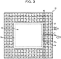
- FIG. 3 is a plan view of the package board according to Embodiment 1.
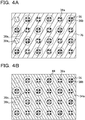
- FIG. 4A is an enlarged view of a region A of FIG. 3
- FIG. 4B is a perspective view of the resist film of FIG. 4A .
- FIG. 3 is a plan view of a lower surface side of the package board 30 to which the bumps 70 are coupled.
- an outline of a region 52 in which the electronic component 50 is projected onto the package board 30 is illustrated by a broken line, and a flow of the currents supplied from the power source 20 is illustrated by a white arrow.
- a plurality of ground pads 38a and a plurality of power source pads 38b are provided so as to surround a capacitor region 42 in which the capacitor 40 is mounted.
- the plurality of ground pads 38a and the plurality of power source pads 38b are alternately lined up lengthwise and breadthwise and arranged in a lattice shape.
- the plurality of ground pads 38a has sizes identical to each other.
- the plurality of power source pads 38b has sizes identical to each other.
- the ground pads 38a and the power source pads 38b may have sizes identical to each other or sizes different from each other.
- the identical sizes are not limited to a case where the sizes are completely identical, and includes a case where the sizes are different to an extent of a manufacturing error.
- the ground pads 38a are portions of the ground wiring layer 34a which is a solid film provided on the lower surface of the package board 30 which are exposed through the openings of the resist film 76.
- the power source pads 38b are located in the openings provided in the ground wiring layer 34a, and gaps 44 are provided between the power source pads and the ground wiring layer 34a. Accordingly, the ground pads 38a and the power source pads 38b are not electrically coupled.
- the ground pads 38a and the power source pads 38b are metal films in regions to which the bumps 70 are bonded and are metal films in regions exposed through the openings of the resist film 76.
- the ground pads 38a include ground pads 38a 1 with which the vias 36 are in contact and ground pads 38a 2 with which the vias 36 are not in contact.
- the ground pads 38a 1 are illustrated in white, and the ground pads 38a 2 are illustrated in black.
- one or a plurality of ground pads 38a 1 with which the via 36 is in contact and one or a plurality of ground pads 38a 2 with which the via 36 is not in contact are included in a column 46 adjacent to the capacitor region 42 among a plurality of columns formed by the plurality of pads 38.
- the ground pads 38a 2 are arranged in a central portion of a side of an outline of the capacitor region 42.
- the ground pads 38a 2 are not arranged at ends of the side of the outline of the capacitor region 42.
- the electronic apparatus of Comparative Example 2 is different from the electronic apparatus 100 of Embodiment 1 in that all the ground pads 38a are constituted by the ground pads 38a 1 in contact with the via 36. Otherwise, the electronic apparatus of Comparative Example 2 has a configuration identical to the configuration of the electronic apparatus 100 of Embodiment 1.
- the simulation was performed under the following conditions.
- the printed board 10 was made of an FR4 substrate, and 12 wiring layers 14 were laminated.
- the wiring layers 14, the vias 16, and the pads 18 were made of copper.
- the package board 30 was made of an organic material containing an epoxy resin as a main component, and 12 wiring layers 34 were laminated.
- the wiring layers 34, the vias 36, and the pads 38 are made of copper.
- the bumps 70 were solder balls and had a pitch interval of 1 mm. For this structure, current values flowing through the bumps 70 bonded to the ground pads 18a and 38a were calculated when a current consumed by the electronic component 50 was 200 A.
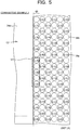
- FIG. 5 illustrates a simulation result of the electronic apparatus according to Comparative Example 2.
- FIG. 6 illustrates a simulation result of the electronic apparatus according to Embodiment 1.
- current values (unit: A) flowing through the bumps 70 are illustrated in the ground pads 38a.
- FIG. 5 in the electronic apparatus of Comparative Example 2, a result in which the currents concentratedly flow to the bumps 70 bonded to the ground pads 38a in a region 54 adjacent to the capacitor region 42 and located in the central portion of the side of the outline of the capacitor region 42 was obtained.
- a maximum current value was 1.90 A.
- FIG. 5 illustrates a simulation result of the electronic apparatus according to Comparative Example 2.
- the currents flowing through the bumps 70 bonded to the ground pads 38a in the region 54 were smaller than the currents in the electronic apparatus of Comparative Example 2. Instead, the currents flowing through the bumps 70 bonded to the ground pads 38a adjacent to the ground pads 38a in the region 54 in the identical column 46 are larger than the currents of the electronic apparatus of Comparative Example 2. A maximum current value was 1.72 A.
- the current values flowing through the bumps 70 bonded to the ground pads 38a in the region 54 were smaller than the current values in the electronic apparatus of Comparative Example 2. This is considered to be due to the following reasons.
- the ground pads 38a in the region 54 are the ground pads 38a 2 not in contact with the via 36.
- the currents are hard to flow through the bumps 70 bonded to the ground pads 38a 2 and the currents are distributed and flow to the bumps 70 bonded to the ground pads 38a 1 around the ground pads 38a 2 .
- the current values flowing through the bumps 70 bonded to the ground pads 38a 2 decrease.
- the plurality of ground pads 38a includes the ground pad 38ai in contact with the via 36 and the ground pads 38a 2 not in contact with the via 36 in the column 46 which is adjacent to the capacitor region 42 and is along the side of the capacitor region 42.
- the concentration of the currents on some bumps 70 among the plurality of bumps 70 may be relaxed.
- the reliability of the bumps 70 may be improved.
- the via 36 may be in contact with the ground pads 38a 2 in an area smaller than an area of the ground pads 38a 1 .
- the plurality of ground pads 38a may include the ground pads 38a 1 with which the via 36 is in contact and the ground pad 38a 2 of which a total area in contact with the via 36 is smaller than a total area of the ground pads 38a 1 in contact with the via 36 in the column 46.
- the current concentration may be relaxed.
- the ground pads 38a 2 may be arranged in the central portion of the side of the outline of the capacitor region 42 and may not be arranged at the ends.
- the concentration of the currents on some bumps 70 may be relaxed, and the stability of the supply of the power of the fixed voltage to the electronic component 50 may be improved by reducing the number of the ground pads 38a 2 with which the via 36 is not in contact.
- the ground pads 38a 2 are provided so as to be located at a side located on an upstream side of the currents supplied from the power source 20 among the sides of the outline of the capacitor region 42. Accordingly, the concentration of the currents on the bumps 70 in the portions in which the wiring distance between the power source 20 and the electronic component 50 is easy to be short (for example, a wiring resistance is easy to be small) may be effectively relaxed.
- FIG. 7 is a plan view of a package board according to Embodiment 2. Similar to FIG. 3 , FIG. 7 illustrates a plan view of a lower surface side of a package board 30a to which bumps 70 are coupled. As illustrated in FIG. 7 , in Embodiment 2, ground pads 38a 2 are arranged from one end to the other end of a side of an outline of a capacitor region 42. Other configurations of the electronic apparatus according to Embodiment 2 are identical to the configurations in Embodiment 1, and thus, the illustration and description thereof are omitted.
- FIG. 8 illustrates a simulation result of the electronic apparatus according to Embodiment 2.
- current values (unit: A) flowing through the bumps 70 are illustrated in ground pads 38a.
- a simulation was performed under conditions identical to the conditions described in Embodiment 1.
- the currents flowing through the bumps 70 bonded to the ground pads 38a in a column 46 decreases, and a maximum current value is 1.46 A.
- the bump 70 having the maximum current value was a bump coupled to the ground pad 38a located in the vicinity of the center of the side of the outline of the capacitor region 42. It is considered that since the ground pads 38a 2 are provided from one end to the other end of the side of the outline of the capacitor region 42, the currents flowing through the bumps 70 bonded to the ground pads 38a in the column 46 decrease.
- the ground pads 38a 2 are arranged from one end to the other end of the side of the outline of the capacitor region 42.
- the currents flowing through the plurality of bumps 70 may be further distributed, and the concentration of the currents on some bumps 70 may be further relaxed.
- FIG. 9 is a plan view of a package board according to Embodiment 3. Similar to FIG. 3 , FIG. 9 illustrates a plan view of a lower surface side of a package board 30b to which bumps 70 are coupled. As illustrated in FIG. 9 , in Embodiment 3, ground pads 38a 2 are arranged so as to surround a capacitor region 42. Other configurations of the electronic apparatus according to Embodiment 3 are identical to the configurations in Embodiment 1, and thus, the illustration and description thereof are omitted.
- the ground pads 38a 2 are arranged so as to surround the capacitor region 42. Accordingly, the concentration of the currents on some bumps 70 may be further relaxed.
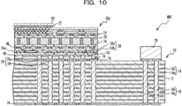
- FIG. 10 is a cross-sectional view of an electronic apparatus according to Embodiment 4.
- FIG. 11 is a plan view of a package board according to Embodiment 4.
- FIG. 11 is a plan view of a lower surface side of a package board 30c to which bumps 70 are coupled.
- ground pads 38a 2 are arranged from one end to the other end of a side of an outline of a capacitor region 42.
- a ground wiring layer 34a provided in the capacitor region 42 is not in contact with via 36 in at least a partial region 48 of regions located beside a column 46 adjacent to the capacitor region 42.
- a region in which the via 36 is not provided is expanded from the column 46 to the capacitor region 42.
- a length of the region 48 in a direction along the column 46 is longer than a length of one of the ground pad 38a and the power source pad 38b.
- the length of the region 48 in the direction along the column 46 is longer than a diameter of one bump 70.
- the region 48 is located so as to include a central portion of the side of the outline of the capacitor region 42.
- Other configurations are identical to the configurations in Embodiment 1, and thus, the illustration and description thereof are omitted.
- FIG. 12 illustrates a simulation result of the electronic apparatus according to Embodiment 4.
- current values (unit: A) flowing through the bumps 70 are illustrated in the ground pads 38a.
- a length L of the region 48 in which the via 36 is not provided was set to 11 mm, and a width W was set to 1 mm.
- the other conditions were identical to the conditions described in Embodiment 1.
- the current values flowing through the bumps 70 bonded to the ground pads 38a in the column 46 further decrease, and a maximum current value is 1.29 A.
- the bump 70 having the maximum current value was the bump 70 coupled to the ground pad 38a located in the vicinity of the center of the side of the outline of the capacitor region 42. It is considered that since the ground wiring layer 34a is not in contact with the via 36 in the region 48, the currents flowing through the bumps 70 bonded to the ground pads 38a in the column 46 decrease.
- the ground wiring layer 34a provided in the capacitor region 42 is not in contact with the via 36 in at least a partial region 48 of regions adjacent to the column 46.
- the concentration of the currents on some bumps 70 may be further relaxed.
- the length L of the region 48 of the ground wiring layer 34a provided in the capacitor region 42 with which the via 36 is not in contact in the direction along the column 46 is longer than a length of one of the ground pad 38a and the power source pad 38b.
- the concentration of the currents on some bumps 70 may be effectively relaxed.
- the length L of the region 48 in the direction along the column 46 is preferably three times or more, more preferably five times or more, and further preferably seven times or more the length of one of the ground pad 38a and the power source pad 38b.
- the region 48 may extend from one to the other of a pair of sides of the outline of the capacitor region 42.
- the length L of the region 48 along the column 46 may be identical to a length of the side of the outline of the capacitor region 42.
- the region 48 may be provided so as to round once along the side of the outline of the capacitor region 42.
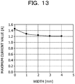
- FIG. 13 illustrates a simulation result representing a relationship between the width W of the region 48 with which the via 36 is not in contact and the maximum value of the currents flowing through the bumps 70.
- a result in which the maximum current value decreases as the width W increased until the width W of the region 48 becomes 3 mm was obtained.
- a result in which when the width W of the region 48 exceeds 3 mm, the maximum current value hardly decreases was obtained.
- the width W of the region 48 of the ground wiring layer 34a provided in the capacitor region 42 with which the via 36 is not in contact in the direction intersecting the direction along the column 46 is wider than 0 mm and equal to or narrower than 3.0 mm.
- a region of the ground wiring layer 34a provided in the capacitor region 42 which is large than 0 mm and equal to or smaller than 3.0 mm from an end in the column 46 close to the ground pad 38a is set as the region 48 with which the via 36 is not in contact. Accordingly, an increase in the region in which the via 36 is not provided may be suppressed while relaxing the concentration of the currents on some bumps 70.
- the stability of the supply of the power of the fixed voltage to the electronic component 50 may be improved.
- the width W of the region 48 is more preferably wider than 0 mm and equal to or narrower than 2.5 mm, and further preferably wider than 0 mm and equal to or narrower than 2.0 mm.
- the region 48 of the ground wiring layer 34a provided in the capacitor region 42 with which the via 36 is not in contact is located so as to include the central portion of the side of the outline of the capacitor region 42.
- the plurality of ground pads 38a includes the ground pads 38a 1 with which the via 36 is in contact and the ground pads 38a 2 of which the total area in contact with the via 36 is smaller than the total area of the ground pad 38a 1 in contact with the via in the column 46 adjacent to the capacitor region 42 has been described as an example in Embodiment 1 to Embodiment 4.
- the present disclosure is not limited to this case, and the same may apply to the power source pads 38b instead of the ground pads 38a or in addition to the ground pads 38a.
- the plurality of power source pads 38b may include first power source pads with which the via 36 is in contact and second power source pads of which a total area in contact with the via 36 is smaller than a total area of the first power source pads in contact with the via 36 in the column 46 adjacent to the capacitor region 42.
- the concentration of the currents on some bumps 70 may also be relaxed.
- the wiring layer provided in the capacitor region 42 is the ground wiring layer 34a electrically coupled to the ground pads 38a 2
- the present disclosure is not limited to this case.
- the wiring layer provided in the capacitor region 42 may be the power source wiring layer electrically coupled to the second power source pads.
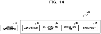
- FIG. 14 is a block diagram illustrating a design support apparatus.
- design information 80 is input to a board design support apparatus 500 from a graphic processing system such as a CAD system.
- the board design support apparatus 500 includes an analysis unit 81, a determination unit 82, a correction unit 83, and a display unit 84.
- FIG. 15 is a block diagram when the board design support apparatus is achieved by a computer.
- a computer 510 includes a CPU 85, a memory 86, and a nonvolatile storage unit 87.
- the CPU 85, the memory 86, and the storage unit 87 are coupled to each other through a bus 88.
- the computer 510 includes a display 89, a keyboard 90, and a mouse 91 which are also coupled to the bus 88.
- An interface (I/O) 93 for coupling the computer 510 to a computer network or the like and a device (R/W) 92 into which a storage medium is inserted to read and write data from and to the inserted storage medium are coupled to the bus 88.
- the storage unit 87 stores a design support program 94 for causing the computer 510 to function as the board design support apparatus 500.
- the design support program 94 includes an analysis process 95, a determination process 96, and a correction process 97.
- the CPU 85 reads out the design support program 94 from the storage unit 87, loads the design support program into the memory 86, and executes the processes of the design support program 94.
- the computer 510 operates as the board design support apparatus 500.
- the CPU 85 operates as the analysis unit 81, the determination unit 82, or the correction unit 83 by executing the analysis process 95, the determination process 96, or the correction process 97.
- FIG. 16 is a flowchart illustrating an example of the method for supporting the design of the package board.
- the CPU 85 acquires initial design information (layout pattern) of the printed board 10 and the package board 30, and calculates initial values of the currents flowing through the plurality of bumps 70 (step S10). Subsequently, the CPU 85 determines whether or not the current values of the plurality of bumps 70 is within a predetermined value (step S12).
- the predetermined value may be an allowable current value of the bump 70, for example, a current value that is a threshold value for determining whether or not disconnection occurs in the bump 70.
- the predetermined value is stored, for example, in the storage unit 87.
- the CPU 85 stores the design information of the package board 30 as current design information (in this example, initial design information) in the storage unit 87 (step S30). Thereafter, the processing is terminated.
- the via 36 in contact with at least one of the ground pad 38a and the power source pad 38b to which the bump 70 having the current value exceeding the predetermined value is coupled is deleted (step S14). For example, the via 36 in contact with the ground pad 38a or the power source pad 38b to which the bump 70 having the maximum current value is coupled is deleted.
- the CPU 85 calculates the current values of the plurality of bumps 70 and determines whether or not the current values fall within the predetermined value (step S16).
- the CPU 85 stores the design information of the package board 30 as the current design information in the storage unit 87 (step S30). Thereafter, the processing is terminated.
- the processing proceeds to step S18.
- step S18 the CPU 85 determines whether or not the via 36 in contact with the ground pad 38a adjacent to the ground pad 38a from which the via 36 is deleted or the power source pad 38b adjacent to the power source pad 38b from which the via 36 is deleted is able to be deleted (step S18).
- a case where the via 36 is not able to be deleted is, for example, a case where there is no adjacent ground pad 38a or power source pad 38b.
- a case where there is the adjacent pad may be a case where there is the adjacent pad in the column 46 in FIG. 3 , and may be a case where there is an adjacent pad on one side or there are adjacent pads on both sides.
- step S18 When the via 36 is not able to be deleted (No in step S18), the processing proceeds to step S22.
- the CPU 85 determines whether or not the bump 70 having the maximum current value calculated in step S16 is the bump located in the vicinity of the bump 70 having the maximum current value calculated in step S10 (step S20).
- a case where the bump is located in the vicinity includes, for example, a case where the bump is located adjacent to each other by one or two.
- step S20 the CPU 85 returns the processing to step S14, and deletes the via 36 in contact with the ground pad 38a adjacent to the ground pad 38a from which the via 36 is deleted or the power source pad 38b adjacent to the power source pad 38b from which the via 36 is deleted.
- the processing proceeds to step S22.
- step S22 the CPU 85 deletes the via 36 over the wiring layer 34 provided in the capacitor region 42 inside the ground pad 38a or the power source pad 38b (step S22). For example, in an initial stage, the via 36 in a region adjacent to the ground pad 38a or the power source pad 38b to which the bump 70 having the maximum current value calculated in step S10 is coupled in the wiring layer 34 provided in the capacitor region 42 is deleted. When the processing returns from step S26 to be described later, the via 36 located adjacent to the deleted via 36 in the direction along the column 46 is deleted. For example, the region 48 of the wiring layer 34 provided in the capacitor region 42 which is not in contact with the via 36 is expanded from the central portion to the ends of the side of the outline of the capacitor region 42.
- the CPU 85 calculates the current values of the plurality of bumps 70 and determines whether or not the current values fall within the predetermined value (step S24).
- the CPU 85 stores the design information of the package board 30 as the current design information in the storage unit 87 (step S30). Thereafter, the processing is terminated.
- step S26 determines whether or not the via 36 over the wiring layer 34 provided in the capacitor region 42 is able to be further deleted.
- the determination of whether or not the via 36 is able to be further deleted is performed depending on, for example, whether or not there is the via 36 in a region in which it is effective to decrease the maximum current value as described in Embodiment 3, or the like.
- the CPU 85 returns the processing to step S22 and repeats step S22 to step S26.
- the via 36 is not able to be deleted (No in step S26)
- the CPU 85 displays an error on the display 89 (step S28), and terminates the processing.
- step S14 Although a case where the via 36 in contact with the ground pad 38a or the power source pad 38b is deleted in step S14 has been described as an example in FIG. 16 , the total area of the via 36 in contact with the ground pad 38a or the power source pad 38b may be reduced.
- step S10 magnitudes of the currents flowing through the plurality of bumps 70 are obtained.
- the design information of the package board 30 is corrected such that the magnitudes of the currents are within the predetermined value by decreasing the total area of the ground pad 38a or the power source pad 38b in contact with the via 36 to which the bump 70 exceeding the predetermined value is coupled (steps S14, S16, and S30). Accordingly, the concentration of the currents on some bumps 70 may be relaxed.
- the current value may not be within the predetermined value (No in step S16).
- the design information of the package board 30 is corrected such that the current value is within the predetermined value by deleting the via 36 in contact with the wiring layer 34 provided in the capacitor region 42 (steps S22, S24, and S30). Accordingly, the concentration of the currents on some bumps 70 may be relaxed.
Landscapes
- Engineering & Computer Science (AREA)
- Physics & Mathematics (AREA)
- Computer Hardware Design (AREA)
- Theoretical Computer Science (AREA)
- Geometry (AREA)
- Computer Networks & Wireless Communication (AREA)
- Evolutionary Computation (AREA)
- General Engineering & Computer Science (AREA)
- General Physics & Mathematics (AREA)
- Microelectronics & Electronic Packaging (AREA)
- Production Of Multi-Layered Print Wiring Board (AREA)
- Structure Of Printed Boards (AREA)
Abstract
Description
- The embodiments discussed herein are related to an electronic device, an electronic apparatus, and a method for supporting a design of an electronic device.
- A method for coupling boards to each other by a bump such as a solder ball has been known. A method for improving uniformity of a current density in the solder ball by setting an area density of a via to be higher in a central region of a pad than in a peripheral region thereof so as to suppress formation of a void in the solder ball due to electromigration has been known (for example, PTL 1).
- PTL 1:
Japanese Laid-open Patent Publication No. 2010-251754 - When a first board at which an electronic component is mounted is mounted at a second board by a plurality of bumps, currents may flow concentratedly to some bumps of the plurality of bumps. In this case, a current exceeding an allowable current may flow to the bump at which the current concentrates, and damage such as disconnection may occur.
- In one aspect, it is an object to relax concentration of currents on some bumps.
- In one aspect, there is provided an electronic device including a board that includes an insulating film, a wiring layer and a via provided in the insulating film, and a plurality of power source pads and a plurality of ground pads which are provided in the insulating film so as to surround a capacitor region in which a capacitor is provided and to which a plurality of bumps is coupled, and an electronic component that is mounted at the board, and is electrically coupled to the plurality of power source pads and the plurality of ground pads through the wiring layer and the via. At least one of a case where the plurality of power source pads includes one or a plurality of first power source pads with which the via is in contact and one or a plurality of second power source pads of which a total area in contact with the via is smaller than a total area of the one or plurality of first power source pads in contact with the via in a column lined up along a side of an outline of the capacitor region so as to be adjacent to the capacitor region and a case where the plurality of ground pads includes one or a plurality of first ground pads with which the via is in contact and one or a plurality of second ground pads of which a total area in contact with the via is smaller than a total area of the one or plurality of first ground pads in contact with the via in the column lined up along the side of the outline of the capacitor region so as to be adjacent to the capacitor region is satisfied.
- In one aspect, there is provided an electronic apparatus including a first board, a second board that includes an insulating film, a wiring layer and a via provided in the insulating film, and a plurality of power source pads and a plurality of ground pads provided in the insulating film so as to surround a capacitor region in which a capacitor is provided, and is mounted at the first board by a plurality of bumps being coupled to the plurality of power source pads and the plurality of ground pads, and an electronic component that is mounted at the second board, and is electrically coupled to the plurality of power source pads and the plurality of ground pads through the wiring layer and the via. At least one of a case where the plurality of power source pads includes one or a plurality of first power source pads with which the via is in contact and one or a plurality of second power source pads of which a total area in contact with the via is smaller than a total area of the one or plurality of first power source pads in contact with the via in a column lined up along a side of an outline of the capacitor region so as to be adjacent to the capacitor region and a case where the plurality of ground pads includes one or a plurality of first ground pads with which the via is in contact and one or a plurality of second ground pads of which a total area in contact with the via is smaller than a total area of the one or plurality of first ground pads in contact with the via in the column lined up along the side of the outline of the capacitor region so as to be adjacent to the capacitor region is satisfied.
- In one aspect, there is provided a method for supporting a design of an electronic device that includes a board, which includes an insulating film, a wiring layer and a via provided in the insulating film, and a plurality of power source pads and a plurality of ground pads which are provided in the insulating film so as to surround a capacitor region in which a capacitor is provided and to which a plurality of bumps is coupled, and an electronic component which is mounted at the board and is electrically coupled to the plurality of power source pads and the plurality of ground pads through the wiring layer and the via. The method includes, by using a computer, obtaining magnitudes of currents flowing through the plurality of bumps, and correcting, when there is the bump of which the magnitude of the current exceeds a predetermined value among the plurality of bumps, design information of the board such that the magnitudes of the currents flowing through the plurality of bumps are in the predetermined value by decreasing a total area with which at least one of the power source pad and the ground pad to which the bump exceeding the predetermined value is coupled is in contact with the via among the plurality of power source pads and the plurality of ground pads. Advantageous Effects of Invention
- In one aspect, concentration of currents on some bumps may be relaxed.
-
- [
FIG. 1] FIG. 1A is a cross-sectional view of an electronic apparatus according to Comparative Example 1, andFIG. 1B is a cross-sectional view taken along a line I-I ofFIG. 1A . - [
FIG. 2] FIG. 2 is a cross-sectional view of an electronic apparatus according toEmbodiment 1. - [
FIG. 3] FIG. 3 is a plan view of a package board according to Embodiment 1. - [
FIG. 4] FIG. 4A is an enlarged view of a region A ofFIG. 3 , andFIG. 4B is a perspective view of a resist film ofFIG. 4A . - [
FIG. 5] FIG. 5 illustrates a simulation result of an electronic apparatus according to Comparative Example 2. - [
FIG. 6] FIG. 6 illustrates a simulation result of the electronic apparatus according toEmbodiment 1. - [
FIG. 7] FIG. 7 is a plan view of a package board according to Embodiment 2. - [
FIG. 8] FIG. 8 illustrates a simulation result of an electronic apparatus according toEmbodiment 2. - [
FIG. 9] FIG. 9 is a plan view of a package board according to Embodiment 3. - [
FIG. 10] FIG. 10 is a cross-sectional view of an electronic apparatus according to Embodiment 4. - [
FIG. 11] FIG. 11 is a plan view of a package board according to Embodiment 4. - [
FIG. 12] FIG. 12 illustrates a simulation result of the electronic apparatus according toEmbodiment 4. - [
FIG. 13] FIG. 13 illustrates a simulation result representing a relationship between a width of a region in which a via is not in contact and a maximum current value flowing through a bump. - [
FIG. 14] FIG. 14 is a block diagram illustrating a design support apparatus. - [
FIG. 15] FIG. 15 is a block diagram when a board design support apparatus is achieved by a computer. - [
FIG. 16] FIG. 16 is a flowchart illustrating an example of a method for supporting a design of the package board. - Hereinafter, embodiments of the present invention will be described with reference to the drawings.
- First, an electronic apparatus according to Comparative Example 1 will be described.
FIG. 1A is a cross-sectional view of an electronic apparatus according to Comparative Example 1, andFIG. 1B is a cross-sectional view taken along a line I-I ofFIG. 1A . As illustrated inFIG. 1A , anelectronic apparatus 1000 according to Comparative Example 1 includes a printedboard 10, apackage board 30, and anelectronic component 50. Thepackage board 30 is mounted at the printedboard 10 by a plurality ofbumps 70. Theelectronic component 50 is mounted at thepackage board 30 by a plurality ofbumps 72. Apower source 20 is provided on the printedboard 10. Theelectronic component 50 is electrically coupled to thepower source 20 throughwiring layers 14,vias 16, andpads 18 provided at aninsulating film 12 of the printedboard 10 andwiring layers 34 andvias 36 provided at aninsulating film 32 of thepackage board 30. As illustrated inFIG. 1B , thevia 36 is provided immediately above each of the plurality ofbumps 70 arranged in a lattice shape. - In Comparative Example 1, currents supplied from the
power source 20 are easy to concentratedly flow toinner bumps 70a inFIG. 1A , and are easy to concentratedly flow tobumps FIG. 1B . This is considered to be due to the following reasons. For example,vias 16a coupled to thebumps 70a are vias coupled to thewiring layers 14 on a downstream side in a direction in which the currents supplied from thepower source 20 flow through thewiring layers 14. Thus, it is considered that the currents are hard to flow to a downstream side of portions of thewiring layers 14 at which thevias 16a are coupled, and as a result, the currents concentratedly flow to thevias 16a. In thebumps power source 20 and theelectronic component 50 is easy to be shorter and a resistance is easy to be lower than those in the other bumps 70. Thus, it is considered that the currents are easy to concentrate on thebumps power source 20 increases, it is considered that a large amount of currents also flows tobumps bumps - When the current concentratedly flows to the
bumps 70a, currents exceeding an allowable current flow to thebumps 70a, and damage such as disconnection may occur. For example, a current density of thebumps 70a increases, disconnection due to electromigration may occur. Thus, embodiments in which the concentration of the currents on some bumps of the plurality ofbumps 70 may be suppressed will be described below. -
FIG. 2 is a cross-sectional view of an electronic apparatus according toEmbodiment 1.FIG. 2 illustrates a part of the electronic apparatus ofEmbodiment 1 for clarification of the drawing. As illustrated inFIG. 2 , an electronic apparatus 100 according toEmbodiment 1 includes a printedboard 10, apackage board 30, and anelectronic component 50. - The printed
board 10 includes an insulatingfilm 12, wiring layers 14 extending in a direction intersecting a thickness direction of the insulatingfilm 12, vias 16 extending in the thickness direction of the insulatingfilm 12, andpads 18 provided at upper and lower surfaces of the insulatingfilm 12. Apower source 20 is mounted at the upper surface of the insulatingfilm 12. Thepower source 20 is a power source unit that supplies a power such as a DC-DC converter. Thepads 18 includeground pads 18a coupled to the ground andpower source pads 18b coupled to a power source side of thepower source 20. The wiring layers 14 include ground wiring layers 14a coupled to theground pads 18a and power source wiring layers 14b coupled to thepower source pads 18b. Thevias 16 includeground vias 16a coupled to theground pads 18a and the ground wiring layers 14a and power source vias 16b coupled to thepower source pads 18b and the power source wiring layers 14b. The insulatingfilm 12 is made of an organic material containing a resin material such as, for example, an epoxy resin as a main component or a ceramic material such as aluminum oxide. The wiring layers 14, thevias 16, and thepads 18 are made of metal such as, for example, copper or gold. - Resist
films 74 having openings in regions in which thepads 18 are provided are provided on upper and lower surfaces of the printedboard 10. The resistfilm 74 is, for example, a solder resist film. - The
package board 30 is mounted at the printedboard 10 by a plurality ofbumps 70 such as solder balls. Thepackage board 30 includes an insulatingfilm 32, wiring layers 34 extending in a direction intersecting a thickness direction of the insulatingfilm 32, vias 36 extending in the thickness direction of the insulatingfilm 32, andpads 38 provided at upper and lower surfaces of the insulatingfilm 32. Thepads 38 includeground pads 38a coupled to the ground andpower source pads 38b coupled to the power source side of thepower source 20. Thepackage board 30 is mounted at the printedboard 10 by bonding theground pads 38a to theground pads 18a by thebumps 70 and bonding thepower source pads 38b to thepower source pads 18b by thebumps 70. - The wiring layers 34 include ground wiring layers coupled to the
ground pads 38a and power source wiring layers coupled to thepower source pads 38b. Thevias 36 include ground vias coupled to theground pads 38a and the ground wiring layers and power source vias coupled to thepower source pads 38b and the power source wiring layers. The insulatingfilm 32 is made of an organic material containing a resin material such as, for example, an epoxy resin as a main component or a ceramic material such as aluminum oxide. The wiring layers 34, thevias 36, and thepads 38 are made of metal such as, for example, copper or gold. - A
capacitor 40 is mounted at thepackage board 30. Thecapacitor 40 is, for example, a chip component and is mounted at aground wiring layer 34a provided at the lower surface of the insulatingfilm 32. Only onecapacitor 40 may be provided, or two or more capacitors may be provided. - A resist
film 76 having openings that expose thepads 38 are provided at a lower surface of thepackage board 30. The resistfilm 76 also has an opening that exposes theground wiring layer 34a in a region in which thecapacitor 40 is mounted. The resistfilm 76 is, for example, a solder resist film. Thebumps 70 are bonded to thepads 38 exposed through the openings of the resistfilm 76. - The
electronic component 50 is mounted at an upper surface of thepackage board 30 by a plurality ofbumps 72. Theelectronic component 50 is a semiconductor component such as, for example, large scale integration (LSI), but may be another component. Theelectronic component 50 is electrically coupled to thepads 38 through the wiring layers 34 and thevias 36. For example, theelectronic component 50 is electrically coupled to thepower source 20 mounted at the printedboard 10 and operates by a power supplied from thepower source 20. Thecapacitor 40 is provided to stably supply a power of a fixed voltage to theelectronic component 50. -
FIG. 3 is a plan view of the package board according toEmbodiment 1.FIG. 4A is an enlarged view of a region A ofFIG. 3 , andFIG. 4B is a perspective view of the resist film ofFIG. 4A .FIG. 3 is a plan view of a lower surface side of thepackage board 30 to which thebumps 70 are coupled. InFIG. 3 , an outline of aregion 52 in which theelectronic component 50 is projected onto thepackage board 30 is illustrated by a broken line, and a flow of the currents supplied from thepower source 20 is illustrated by a white arrow. As illustrated inFIG. 3 , a plurality ofground pads 38a and a plurality ofpower source pads 38b are provided so as to surround acapacitor region 42 in which thecapacitor 40 is mounted. The plurality ofground pads 38a and the plurality ofpower source pads 38b are alternately lined up lengthwise and breadthwise and arranged in a lattice shape. The plurality ofground pads 38a has sizes identical to each other. The plurality ofpower source pads 38b has sizes identical to each other. Theground pads 38a and thepower source pads 38b may have sizes identical to each other or sizes different from each other. The identical sizes are not limited to a case where the sizes are completely identical, and includes a case where the sizes are different to an extent of a manufacturing error. - As illustrated in
FIGs. 4(a) and 4(b) , theground pads 38a are portions of theground wiring layer 34a which is a solid film provided on the lower surface of thepackage board 30 which are exposed through the openings of the resistfilm 76. Thepower source pads 38b are located in the openings provided in theground wiring layer 34a, andgaps 44 are provided between the power source pads and theground wiring layer 34a. Accordingly, theground pads 38a and thepower source pads 38b are not electrically coupled. Since thebumps 70 are bonded to theground pads 38a and thepower source pads 38b exposed through the openings of the resistfilm 76, it may be said that theground pads 38a and thepower source pads 38b are metal films in regions to which thebumps 70 are bonded and are metal films in regions exposed through the openings of the resistfilm 76. - The
ground pads 38a includeground pads 38a1 with which thevias 36 are in contact andground pads 38a2 with which thevias 36 are not in contact. InFIG. 3 , theground pads 38a1 are illustrated in white, and theground pads 38a2 are illustrated in black. As illustrated inFIG. 3 , one or a plurality ofground pads 38a1 with which the via 36 is in contact and one or a plurality ofground pads 38a2 with which the via 36 is not in contact are included in acolumn 46 adjacent to thecapacitor region 42 among a plurality of columns formed by the plurality ofpads 38. Theground pads 38a2 are arranged in a central portion of a side of an outline of thecapacitor region 42. Theground pads 38a2 are not arranged at ends of the side of the outline of thecapacitor region 42. - Simulations performed for the electronic apparatus 100 of
Embodiment 1 and an electronic apparatus of Comparative Example 2 will be described. The electronic apparatus of Comparative Example 2 is different from the electronic apparatus 100 ofEmbodiment 1 in that all theground pads 38a are constituted by theground pads 38a1 in contact with the via 36. Otherwise, the electronic apparatus of Comparative Example 2 has a configuration identical to the configuration of the electronic apparatus 100 ofEmbodiment 1. The simulation was performed under the following conditions. The printedboard 10 was made of an FR4 substrate, and 12wiring layers 14 were laminated. The wiring layers 14, thevias 16, and thepads 18 were made of copper. Thepackage board 30 was made of an organic material containing an epoxy resin as a main component, and 12wiring layers 34 were laminated. The wiring layers 34, thevias 36, and thepads 38 are made of copper. Thebumps 70 were solder balls and had a pitch interval of 1 mm. For this structure, current values flowing through thebumps 70 bonded to theground pads electronic component 50 was 200 A. -
FIG. 5 illustrates a simulation result of the electronic apparatus according to Comparative Example 2.FIG. 6 illustrates a simulation result of the electronic apparatus according toEmbodiment 1. InFIGs. 5 and6 , current values (unit: A) flowing through thebumps 70 are illustrated in theground pads 38a. As illustrated inFIG. 5 , in the electronic apparatus of Comparative Example 2, a result in which the currents concentratedly flow to thebumps 70 bonded to theground pads 38a in aregion 54 adjacent to thecapacitor region 42 and located in the central portion of the side of the outline of thecapacitor region 42 was obtained. A maximum current value was 1.90 A. As illustrated inFIG. 6 , in the electronic apparatus 100 ofEmbodiment 1, the currents flowing through thebumps 70 bonded to theground pads 38a in theregion 54 were smaller than the currents in the electronic apparatus of Comparative Example 2. Instead, the currents flowing through thebumps 70 bonded to theground pads 38a adjacent to theground pads 38a in theregion 54 in theidentical column 46 are larger than the currents of the electronic apparatus of Comparative Example 2. A maximum current value was 1.72 A. - As described above, in the electronic apparatus 100 of
Embodiment 1, the current values flowing through thebumps 70 bonded to theground pads 38a in theregion 54 were smaller than the current values in the electronic apparatus of Comparative Example 2. This is considered to be due to the following reasons. For example, inEmbodiment 1, theground pads 38a in theregion 54 are theground pads 38a2 not in contact with the via 36. Thus, it is considered that the currents are hard to flow through thebumps 70 bonded to theground pads 38a2 and the currents are distributed and flow to thebumps 70 bonded to theground pads 38a1 around theground pads 38a2. Thus, it is considered that the current values flowing through thebumps 70 bonded to theground pads 38a2 decrease. - According to
Embodiment 1, as illustrated inFIGs. 3 to 4(b) , the plurality ofground pads 38a includes the ground pad 38ai in contact with the via 36 and theground pads 38a2 not in contact with the via 36 in thecolumn 46 which is adjacent to thecapacitor region 42 and is along the side of thecapacitor region 42. Thus, as illustrated inFIGs. 5 and6 , the concentration of the currents on somebumps 70 among the plurality ofbumps 70 may be relaxed. Thus, the reliability of thebumps 70 may be improved. Although a case where the via 36 is not in contact with theground pads 38a2 has been described as an example inEmbodiment 1, the via 36 may be in contact with theground pads 38a2 in an area smaller than an area of theground pads 38a1. For example, the plurality ofground pads 38a may include theground pads 38a1 with which the via 36 is in contact and theground pad 38a2 of which a total area in contact with the via 36 is smaller than a total area of theground pads 38a1 in contact with the via 36 in thecolumn 46. In this case, since the currents are also hard to flow through thebumps 70 bonded to theground pads 38a2, the current concentration may be relaxed. - As illustrated in
FIG. 5 of Comparative Example 2, large currents are easy to flow through thebumps 70 located in the central portion of the side of the outline of thecapacitor region 42. Accordingly, as illustrated inFIG. 3 , theground pads 38a2 may be arranged in the central portion of the side of the outline of thecapacitor region 42 and may not be arranged at the ends. Thus, the concentration of the currents on somebumps 70 may be relaxed, and the stability of the supply of the power of the fixed voltage to theelectronic component 50 may be improved by reducing the number of theground pads 38a2 with which the via 36 is not in contact. - As illustrated in
FIG. 3 , it is preferable that theground pads 38a2 are provided so as to be located at a side located on an upstream side of the currents supplied from thepower source 20 among the sides of the outline of thecapacitor region 42. Accordingly, the concentration of the currents on thebumps 70 in the portions in which the wiring distance between thepower source 20 and theelectronic component 50 is easy to be short (for example, a wiring resistance is easy to be small) may be effectively relaxed. -
FIG. 7 is a plan view of a package board according toEmbodiment 2. Similar toFIG. 3 ,FIG. 7 illustrates a plan view of a lower surface side of apackage board 30a to which bumps 70 are coupled. As illustrated inFIG. 7 , inEmbodiment 2,ground pads 38a2 are arranged from one end to the other end of a side of an outline of acapacitor region 42. Other configurations of the electronic apparatus according toEmbodiment 2 are identical to the configurations inEmbodiment 1, and thus, the illustration and description thereof are omitted. -
FIG. 8 illustrates a simulation result of the electronic apparatus according toEmbodiment 2. InFIG. 8 , current values (unit: A) flowing through thebumps 70 are illustrated inground pads 38a. A simulation was performed under conditions identical to the conditions described inEmbodiment 1. As illustrated inFIG. 8 , in the electronic apparatus ofEmbodiment 2, the currents flowing through thebumps 70 bonded to theground pads 38a in acolumn 46 decreases, and a maximum current value is 1.46 A. Thebump 70 having the maximum current value was a bump coupled to theground pad 38a located in the vicinity of the center of the side of the outline of thecapacitor region 42. It is considered that since theground pads 38a2 are provided from one end to the other end of the side of the outline of thecapacitor region 42, the currents flowing through thebumps 70 bonded to theground pads 38a in thecolumn 46 decrease. - According to
Embodiment 2, as illustrated inFIG. 7 , theground pads 38a2 are arranged from one end to the other end of the side of the outline of thecapacitor region 42. Thus, as illustrated inFIG. 8 , the currents flowing through the plurality ofbumps 70 may be further distributed, and the concentration of the currents on somebumps 70 may be further relaxed. -
FIG. 9 is a plan view of a package board according toEmbodiment 3. Similar toFIG. 3 ,FIG. 9 illustrates a plan view of a lower surface side of apackage board 30b to which bumps 70 are coupled. As illustrated inFIG. 9 , inEmbodiment 3,ground pads 38a2 are arranged so as to surround acapacitor region 42. Other configurations of the electronic apparatus according toEmbodiment 3 are identical to the configurations inEmbodiment 1, and thus, the illustration and description thereof are omitted. - According to
Embodiment 3, theground pads 38a2 are arranged so as to surround thecapacitor region 42. Accordingly, the concentration of the currents on somebumps 70 may be further relaxed. -
FIG. 10 is a cross-sectional view of an electronic apparatus according toEmbodiment 4.FIG. 11 is a plan view of a package board according toEmbodiment 4.FIG. 11 is a plan view of a lower surface side of apackage board 30c to which bumps 70 are coupled. As illustrated inFIGs. 10 and11 , in anelectronic apparatus 400 according toEmbodiment 4,ground pads 38a2 are arranged from one end to the other end of a side of an outline of acapacitor region 42. Aground wiring layer 34a provided in thecapacitor region 42 is not in contact with via 36 in at least apartial region 48 of regions located beside acolumn 46 adjacent to thecapacitor region 42. As described above, inEmbodiment 4, a region in which the via 36 is not provided is expanded from thecolumn 46 to thecapacitor region 42. A length of theregion 48 in a direction along thecolumn 46 is longer than a length of one of theground pad 38a and thepower source pad 38b. The length of theregion 48 in the direction along thecolumn 46 is longer than a diameter of onebump 70. Theregion 48 is located so as to include a central portion of the side of the outline of thecapacitor region 42. Other configurations are identical to the configurations inEmbodiment 1, and thus, the illustration and description thereof are omitted. -
FIG. 12 illustrates a simulation result of the electronic apparatus according toEmbodiment 4. InFIG. 12 , current values (unit: A) flowing through thebumps 70 are illustrated in theground pads 38a. In the simulation, a length L of theregion 48 in which the via 36 is not provided was set to 11 mm, and a width W was set to 1 mm. The other conditions were identical to the conditions described inEmbodiment 1. As illustrated inFIG. 12 , inEmbodiment 4, the current values flowing through thebumps 70 bonded to theground pads 38a in thecolumn 46 further decrease, and a maximum current value is 1.29 A. Thebump 70 having the maximum current value was thebump 70 coupled to theground pad 38a located in the vicinity of the center of the side of the outline of thecapacitor region 42. It is considered that since theground wiring layer 34a is not in contact with the via 36 in theregion 48, the currents flowing through thebumps 70 bonded to theground pads 38a in thecolumn 46 decrease. - According to
Embodiment 3, as illustrated inFIGs. 10 and11 , theground wiring layer 34a provided in thecapacitor region 42 is not in contact with the via 36 in at least apartial region 48 of regions adjacent to thecolumn 46. Thus, as illustrated inFIG. 12 , the concentration of the currents on somebumps 70 may be further relaxed. - As illustrated in
FIG. 11 , it is preferable that the length L of theregion 48 of theground wiring layer 34a provided in thecapacitor region 42 with which the via 36 is not in contact in the direction along thecolumn 46 is longer than a length of one of theground pad 38a and thepower source pad 38b. Thus, the concentration of the currents on somebumps 70 may be effectively relaxed. From the viewpoint of relaxing the concentration of the currents on somebumps 70, the length L of theregion 48 in the direction along thecolumn 46 is preferably three times or more, more preferably five times or more, and further preferably seven times or more the length of one of theground pad 38a and thepower source pad 38b. Theregion 48 may extend from one to the other of a pair of sides of the outline of thecapacitor region 42. For example, the length L of theregion 48 along thecolumn 46 may be identical to a length of the side of the outline of thecapacitor region 42. Theregion 48 may be provided so as to round once along the side of the outline of thecapacitor region 42. - Next, a simulation for investigating an influence of the width W of the
region 48 on the maximum value of the currents flowing through thebumps 70 will be described. In the simulation, the length L of theregion 48 was fixed to 11 mm, and the width W was changed to 1 mm, 2 mm, 3 mm, or 4 mm. The other conditions were identical to the conditions described inEmbodiment 1.FIG. 13 illustrates a simulation result representing a relationship between the width W of theregion 48 with which the via 36 is not in contact and the maximum value of the currents flowing through thebumps 70. As illustrated inFIG. 13 , a result in which the maximum current value decreases as the width W increased until the width W of theregion 48 becomes 3 mm was obtained. A result in which when the width W of theregion 48 exceeds 3 mm, the maximum current value hardly decreases was obtained. - Based on the simulation result of
FIG. 13 , it is preferable that the width W of theregion 48 of theground wiring layer 34a provided in thecapacitor region 42 with which the via 36 is not in contact in the direction intersecting the direction along thecolumn 46 is wider than 0 mm and equal to or narrower than 3.0 mm. In other words, for example, it is preferable that a region of theground wiring layer 34a provided in thecapacitor region 42 which is large than 0 mm and equal to or smaller than 3.0 mm from an end in thecolumn 46 close to theground pad 38a is set as theregion 48 with which the via 36 is not in contact. Accordingly, an increase in the region in which the via 36 is not provided may be suppressed while relaxing the concentration of the currents on somebumps 70. Thus, the stability of the supply of the power of the fixed voltage to theelectronic component 50 may be improved. From the viewpoint of supplying the current of the fixed voltage to theelectronic component 50, the width W of theregion 48 is more preferably wider than 0 mm and equal to or narrower than 2.5 mm, and further preferably wider than 0 mm and equal to or narrower than 2.0 mm. - As illustrated in
FIG. 5 of Comparative Example 2, large currents are easy to flow through thebumps 70 located in the central portion of the side of the outline of thecapacitor region 42. Accordingly, as illustrated inFIG. 11 , it is preferable that theregion 48 of theground wiring layer 34a provided in thecapacitor region 42 with which the via 36 is not in contact is located so as to include the central portion of the side of the outline of thecapacitor region 42. - A case where the plurality of
ground pads 38a includes theground pads 38a1 with which the via 36 is in contact and theground pads 38a2 of which the total area in contact with the via 36 is smaller than the total area of theground pad 38a1 in contact with the via in thecolumn 46 adjacent to thecapacitor region 42 has been described as an example inEmbodiment 1 toEmbodiment 4. However, the present disclosure is not limited to this case, and the same may apply to thepower source pads 38b instead of theground pads 38a or in addition to theground pads 38a. For example, the plurality ofpower source pads 38b may include first power source pads with which the via 36 is in contact and second power source pads of which a total area in contact with the via 36 is smaller than a total area of the first power source pads in contact with the via 36 in thecolumn 46 adjacent to thecapacitor region 42. In this case, the concentration of the currents on somebumps 70 may also be relaxed. - Although a case where the wiring layer provided in the
capacitor region 42 is theground wiring layer 34a electrically coupled to theground pads 38a2 has been described as an example inEmbodiment 4, the present disclosure is not limited to this case. The wiring layer provided in thecapacitor region 42 may be the power source wiring layer electrically coupled to the second power source pads. - In
Embodiment 5, a method for supporting a design of thepackage board 30 will be described.FIG. 14 is a block diagram illustrating a design support apparatus. As illustrated inFIG. 14 ,design information 80 is input to a boarddesign support apparatus 500 from a graphic processing system such as a CAD system. The boarddesign support apparatus 500 includes ananalysis unit 81, adetermination unit 82, acorrection unit 83, and adisplay unit 84. -
FIG. 15 is a block diagram when the board design support apparatus is achieved by a computer. Acomputer 510 includes aCPU 85, amemory 86, and anonvolatile storage unit 87. TheCPU 85, thememory 86, and thestorage unit 87 are coupled to each other through abus 88. Thecomputer 510 includes adisplay 89, akeyboard 90, and amouse 91 which are also coupled to thebus 88. An interface (I/O) 93 for coupling thecomputer 510 to a computer network or the like and a device (R/W) 92 into which a storage medium is inserted to read and write data from and to the inserted storage medium are coupled to thebus 88. - The
storage unit 87 stores adesign support program 94 for causing thecomputer 510 to function as the boarddesign support apparatus 500. Thedesign support program 94 includes ananalysis process 95, adetermination process 96, and acorrection process 97. TheCPU 85 reads out thedesign support program 94 from thestorage unit 87, loads the design support program into thememory 86, and executes the processes of thedesign support program 94. Thus, thecomputer 510 operates as the boarddesign support apparatus 500. TheCPU 85 operates as theanalysis unit 81, thedetermination unit 82, or thecorrection unit 83 by executing theanalysis process 95, thedetermination process 96, or thecorrection process 97. -
FIG. 16 is a flowchart illustrating an example of the method for supporting the design of the package board. As illustrated inFIG. 16 , theCPU 85 acquires initial design information (layout pattern) of the printedboard 10 and thepackage board 30, and calculates initial values of the currents flowing through the plurality of bumps 70 (step S10). Subsequently, theCPU 85 determines whether or not the current values of the plurality ofbumps 70 is within a predetermined value (step S12). The predetermined value may be an allowable current value of thebump 70, for example, a current value that is a threshold value for determining whether or not disconnection occurs in thebump 70. The predetermined value is stored, for example, in thestorage unit 87. - When the current values of the plurality of
bumps 70 fall within the predetermined value (Yes in step S12), theCPU 85 stores the design information of thepackage board 30 as current design information (in this example, initial design information) in the storage unit 87 (step S30). Thereafter, the processing is terminated. When there is thebump 70 having the current value exceeding the predetermined value (No in step S12), the via 36 in contact with at least one of theground pad 38a and thepower source pad 38b to which thebump 70 having the current value exceeding the predetermined value is coupled is deleted (step S14). For example, the via 36 in contact with theground pad 38a or thepower source pad 38b to which thebump 70 having the maximum current value is coupled is deleted. - Subsequently, the
CPU 85 calculates the current values of the plurality ofbumps 70 and determines whether or not the current values fall within the predetermined value (step S16). When the current values fall within the predetermined value (Yes in step S16), theCPU 85 stores the design information of thepackage board 30 as the current design information in the storage unit 87 (step S30). Thereafter, the processing is terminated. When there is thebump 70 having the current value exceeding the predetermined value (No in step S16), the processing proceeds to step S18. In step S18, theCPU 85 determines whether or not the via 36 in contact with theground pad 38a adjacent to theground pad 38a from which the via 36 is deleted or thepower source pad 38b adjacent to thepower source pad 38b from which the via 36 is deleted is able to be deleted (step S18). A case where the via 36 is not able to be deleted is, for example, a case where there is noadjacent ground pad 38a orpower source pad 38b. A case where there is the adjacent pad may be a case where there is the adjacent pad in thecolumn 46 inFIG. 3 , and may be a case where there is an adjacent pad on one side or there are adjacent pads on both sides. - When the via 36 is not able to be deleted (No in step S18), the processing proceeds to step S22. When the via 36 is able to be deleted (Yes in step S18), the
CPU 85 determines whether or not thebump 70 having the maximum current value calculated in step S16 is the bump located in the vicinity of thebump 70 having the maximum current value calculated in step S10 (step S20). A case where the bump is located in the vicinity includes, for example, a case where the bump is located adjacent to each other by one or two. When thebump 70 is not the bump located in the vicinity (NO in step S20), theCPU 85 returns the processing to step S14, and deletes the via 36 in contact with theground pad 38a adjacent to theground pad 38a from which the via 36 is deleted or thepower source pad 38b adjacent to thepower source pad 38b from which the via 36 is deleted. When thebump 70 is the bump located in the vicinity (Yes in step S20), since it is difficult to decrease the maximum current value even though the via 36 in contact with theadjacent ground pad 38a or the adjacentpower source pad 38b is deleted, the processing proceeds to step S22. - In step S22, the
CPU 85 deletes the via 36 over thewiring layer 34 provided in thecapacitor region 42 inside theground pad 38a or thepower source pad 38b (step S22). For example, in an initial stage, the via 36 in a region adjacent to theground pad 38a or thepower source pad 38b to which thebump 70 having the maximum current value calculated in step S10 is coupled in thewiring layer 34 provided in thecapacitor region 42 is deleted. When the processing returns from step S26 to be described later, the via 36 located adjacent to the deleted via 36 in the direction along thecolumn 46 is deleted. For example, theregion 48 of thewiring layer 34 provided in thecapacitor region 42 which is not in contact with the via 36 is expanded from the central portion to the ends of the side of the outline of thecapacitor region 42. - Subsequently, the
CPU 85 calculates the current values of the plurality ofbumps 70 and determines whether or not the current values fall within the predetermined value (step S24). When the current values fall within the predetermined value (Yes in step S24), theCPU 85 stores the design information of thepackage board 30 as the current design information in the storage unit 87 (step S30). Thereafter, the processing is terminated. - On the other hand, when there is the
bump 70 of which the current value exceeds the predetermined value (No in step S24), theCPU 85 determines whether or not the via 36 over thewiring layer 34 provided in thecapacitor region 42 is able to be further deleted (step S26). The determination of whether or not the via 36 is able to be further deleted is performed depending on, for example, whether or not there is the via 36 in a region in which it is effective to decrease the maximum current value as described inEmbodiment 3, or the like. When the via 36 is able to be deleted (Yes in step S26), theCPU 85 returns the processing to step S22 and repeats step S22 to step S26. When the via 36 is not able to be deleted (No in step S26), theCPU 85 displays an error on the display 89 (step S28), and terminates the processing. - Although a case where the via 36 in contact with the
ground pad 38a or thepower source pad 38b is deleted in step S14 has been described as an example inFIG. 16 , the total area of the via 36 in contact with theground pad 38a or thepower source pad 38b may be reduced. - According to
Embodiment 5, as illustrated inFIG. 16 , magnitudes of the currents flowing through the plurality ofbumps 70 are obtained (step S10). When there is thebump 70 of which the current value exceeds the predetermined value, the design information of thepackage board 30 is corrected such that the magnitudes of the currents are within the predetermined value by decreasing the total area of theground pad 38a or thepower source pad 38b in contact with the via 36 to which thebump 70 exceeding the predetermined value is coupled (steps S14, S16, and S30). Accordingly, the concentration of the currents on somebumps 70 may be relaxed. - As illustrated in
FIG. 16 , even though the total area of theground pad 38a and thepower source pad 38b in contact with the via 36 decreases, the current value may not be within the predetermined value (No in step S16). In this case, it is preferable that the design information of thepackage board 30 is corrected such that the current value is within the predetermined value by deleting the via 36 in contact with thewiring layer 34 provided in the capacitor region 42 (steps S22, S24, and S30). Accordingly, the concentration of the currents on somebumps 70 may be relaxed. - Although a case where the method for supporting the design of the
package board 30 in the flowchart ofFIG. 16 is achieved by thecomputer 510 has been described as an example inEmbodiment 5, the present disclosure is not limited thereto. Various improvements and modifications may be made without departing from the gist described above. Although a case where the program is stored in thestorage unit 87 in advance has been described as an example, the present disclosure is not limited thereto, and the program may be provided in a form of being stored in a storage medium such as a compact disc read-only memory (CD-ROM) or a Digital Versatile Disc (DVD)-ROM. - Although the embodiments of the present invention have been described in detail above, the present invention is not limited to such specific embodiments, and various modifications and changes may be made within the scope of the gist of the present invention described in the claims.
-
- 10 Printed board
- 12 Insulating film
- 14 Wiring layer
- 16 Via
- 18 Pad
- 18a Ground pad
- 18b Power source pad
- 20 Power source
- 30, 30a, 30b, 30c Package board
- 32 Insulating film
- 34 Wiring layer
- 34a Ground wiring layer
- 36 Via
- 38 Pad
- 38a, 38a1, 38a2 Ground pad
- 38b Power source pad
- 40 Capacitor
- 42 Capacitor region
- 44 Gap
- 46 Column
- 48 Region
- 50 Electronic component
- 54 Region
- 70, 72 Bump
- 74, 76 Resist film
- 100, 400, 1000 Electronic apparatus
- 500 Board design support apparatus
- 510 Computer
Claims (11)
- An electronic device comprising:a board that includes an insulating film, a wiring layer and a via provided in the insulating film, and a plurality of power source pads and a plurality of ground pads which are provided in the insulating film so as to surround a capacitor region in which a capacitor is provided and to which a plurality of bumps is coupled; andan electronic component that is mounted at the board, and is electrically coupled to the plurality of power source pads and the plurality of ground pads through the wiring layer and the via,wherein at least one ofa case where the plurality of power source pads includes one or a plurality of first power source pads with which the via is in contact and one or a plurality of second power source pads of which a total area in contact with the via is smaller than a total area of the one or plurality of first power source pads in contact with the via in a column lined up along a side of an outline of the capacitor region so as to be adjacent to the capacitor region anda case where the plurality of ground pads includes one or a plurality of first ground pads with which the via is in contact and one or a plurality of second ground pads of which a total area in contact with the via is smaller than a total area of the one or plurality of first ground pads in contact with the via in the column lined up along the side of the outline of the capacitor region so as to be adjacent to the capacitor region is satisfied.
- The electronic device according to claim 1, wherein at least one of the one or plurality of second power source pads and the one or plurality of second ground pads is not in contact with the via.
- The electronic device according to claim 1 or 2, wherein at least one of the one or plurality of second power source pads and the one or plurality of second ground pads is arranged in a central portion of the side of the outline of the capacitor region, and is not arranged at ends of the side.
- The electronic device according to claim 1 or 2, wherein at least one of the one or plurality of second power source pads and the one or plurality of second ground pads is arranged from one end to the other end of the side of the outline of the capacitor region.
- The electronic device according to claim 1 or 2, wherein at least one of the one or plurality of second power source pads and the one or plurality of second ground pads is arranged so as to surround the capacitor region.
- The electronic device according to any one of claims 1 to 5,
wherein the board includes the wiring layer electrically coupled to the one or plurality of second power source pads and the one or plurality of second ground pads in the capacitor region surrounded by the plurality of power source pads and the plurality of ground pads, and
the wiring layer provided in the capacitor region is not in contact with the via in at least a partial region of regions adjacent to the column. - The electronic device according to claim 6, wherein a length of the at least a partial region in a direction along the column is longer than lengths of one power source pad of the plurality of power source pads and one ground pad of the plurality of ground pads in the direction along the column.
- The electronic device according to claim 6 or 7, wherein a width of the at least a partial region in a direction intersecting the direction along the column is wider than 0 mm and equal to or narrower than 3.0 mm.
- The electronic device according to any one of claims 6 to 8, wherein the at least a partial region is located so as to include a central portion of the side of the outline of the capacitor region.
- An electronic apparatus comprising:a first board;a second board that includes an insulating film, a wiring layer and a via provided in the insulating film, and a plurality of power source pads and a plurality of ground pads provided in the insulating film so as to surround a capacitor region in which a capacitor is provided, and is mounted at the first board by a plurality of bumps being coupled to the plurality of power source pads and the plurality of ground pads; andan electronic component that is mounted at the second board, and is electrically coupled to the plurality of power source pads and the plurality of ground pads through the wiring layer and the via,wherein at least one ofa case where the plurality of power source pads includes one or a plurality of first power source pads with which the via is in contact and one or a plurality of second power source pads of which a total area in contact with the via is smaller than a total area of the one or plurality of first power source pads in contact with the via in a column lined up along a side of an outline of the capacitor region so as to be adjacent to the capacitor region anda case where the plurality of ground pads includes one or a plurality of first ground pads with which the via is in contact and one or a plurality of second ground pads of which a total area in contact with the via is smaller than a total area of the one or plurality of first ground pads in contact with the via in the column lined up along the side of the outline of the capacitor region so as to be adjacent to the capacitor region is satisfied.
- A method for supporting a design of an electronic device that includes a board, which includes an insulating film, a wiring layer and a via provided in the insulating film, and a plurality of power source pads and a plurality of ground pads which are provided in the insulating film so as to surround a capacitor region in which a capacitor is provided and to which a plurality of bumps is coupled, and an electronic component which is mounted at the board and is electrically coupled to the plurality of power source pads and the plurality of ground pads through the wiring layer and the via, the method comprising:by using a computer,obtaining magnitudes of currents flowing through the plurality of bumps; andcorrecting, when there is the bump of which the magnitude of the current exceeds a predetermined value among the plurality of bumps, design information of the board such that the magnitudes of the currents flowing through the plurality of bumps are in the predetermined value by decreasing a total area with which at least one of the power source pad and the ground pad to which the bump exceeding the predetermined value is coupled is in contact with the via among the plurality of power source pads and the plurality of ground pads.
Applications Claiming Priority (1)
| Application Number | Priority Date | Filing Date | Title |
|---|---|---|---|
| PCT/JP2018/034611 WO2020059041A1 (en) | 2018-09-19 | 2018-09-19 | Electronic device, electronic apparatus, and design assistance method for electronic device |
Publications (3)
| Publication Number | Publication Date |
|---|---|
| EP3855482A1 true EP3855482A1 (en) | 2021-07-28 |
| EP3855482A4 EP3855482A4 (en) | 2021-12-08 |
| EP3855482B1 EP3855482B1 (en) | 2026-05-06 |
Family
ID=69886985
Family Applications (1)
| Application Number | Title | Priority Date | Filing Date |
|---|---|---|---|
| EP18933785.0A Active EP3855482B1 (en) | 2018-09-19 | 2018-09-19 | Electronic device, electronic apparatus, and design assistance method for electronic device |
Country Status (4)
| Country | Link |
|---|---|
| US (1) | US11658106B2 (en) |
| EP (1) | EP3855482B1 (en) |
| JP (1) | JP7001175B2 (en) |
| WO (1) | WO2020059041A1 (en) |
Families Citing this family (3)
| Publication number | Priority date | Publication date | Assignee | Title |
|---|---|---|---|---|
| US12160952B2 (en) * | 2022-09-23 | 2024-12-03 | Qualcomm Incorporated | Providing a lower inductance path in a routing substrate for a capacitor, and related electronic devices and fabrication methods |
| US20240379522A1 (en) * | 2023-05-09 | 2024-11-14 | Juniper Networks, Inc. | Semiconductor package with two substrates |
| CN118919513B (en) * | 2024-07-23 | 2025-10-31 | 飞腾信息技术有限公司 | Packaging substrate and packaging device |
Family Cites Families (17)
| Publication number | Priority date | Publication date | Assignee | Title |
|---|---|---|---|---|
| JP2003264253A (en) * | 2002-03-12 | 2003-09-19 | Shinko Electric Ind Co Ltd | Semiconductor device and manufacturing method thereof |
| JP2004006488A (en) * | 2002-05-31 | 2004-01-08 | Nec Engineering Ltd | Printed wiring board and mounting machine using the same |
| JP2004006513A (en) * | 2002-05-31 | 2004-01-08 | Nec Corp | Semiconductor integrated circuit, printed wiring board and electronic equipment |
| US7738259B2 (en) | 2004-01-22 | 2010-06-15 | Alcatel Lucent | Shared via decoupling for area arrays components |
| US7185799B2 (en) * | 2004-03-29 | 2007-03-06 | Intel Corporation | Method of creating solder bar connections on electronic packages |
| JP4387231B2 (en) * | 2004-03-31 | 2009-12-16 | 新光電気工業株式会社 | Capacitor-mounted wiring board and manufacturing method thereof |
| JP4551730B2 (en) * | 2004-10-15 | 2010-09-29 | イビデン株式会社 | Multilayer core substrate and manufacturing method thereof |
| JP2006147676A (en) * | 2004-11-17 | 2006-06-08 | Nec Corp | Wiring board for semiconductor integrated circuit package and semiconductor integrated circuit device using the wiring board |
| JP4452217B2 (en) | 2005-07-04 | 2010-04-21 | 富士通マイクロエレクトロニクス株式会社 | Semiconductor device |
| JP5230997B2 (en) * | 2007-11-26 | 2013-07-10 | 新光電気工業株式会社 | Semiconductor device |
| US8084858B2 (en) | 2009-04-15 | 2011-12-27 | International Business Machines Corporation | Metal wiring structures for uniform current density in C4 balls |
| US8605397B2 (en) * | 2009-05-07 | 2013-12-10 | Rambus Inc. | Configurable, power supply voltage referenced single-ended signaling with ESD protection |
| JP5658640B2 (en) * | 2011-09-12 | 2015-01-28 | ルネサスエレクトロニクス株式会社 | Semiconductor device |
| JP2016066699A (en) * | 2014-09-25 | 2016-04-28 | 京セラサーキットソリューションズ株式会社 | Composite wiring board and mounting structure thereof |
| US9609749B2 (en) * | 2014-11-14 | 2017-03-28 | Mediatek Inc. | Printed circuit board having power/ground ball pad array |
| JP6818534B2 (en) * | 2016-12-13 | 2021-01-20 | キヤノン株式会社 | Printed wiring board, printed circuit board and electronic equipment |
| US20180184524A1 (en) * | 2016-12-27 | 2018-06-28 | Innovium, Inc. | Mixed ball grid array pitch for integrated circuit package |
-
2018
- 2018-09-19 JP JP2020547515A patent/JP7001175B2/en active Active
- 2018-09-19 WO PCT/JP2018/034611 patent/WO2020059041A1/en not_active Ceased
- 2018-09-19 EP EP18933785.0A patent/EP3855482B1/en active Active
-
2021
- 2021-02-24 US US17/183,405 patent/US11658106B2/en active Active
Also Published As
| Publication number | Publication date |
|---|---|
| JP7001175B2 (en) | 2022-01-19 |
| EP3855482A4 (en) | 2021-12-08 |
| EP3855482B1 (en) | 2026-05-06 |
| US11658106B2 (en) | 2023-05-23 |
| US20210183759A1 (en) | 2021-06-17 |
| JPWO2020059041A1 (en) | 2021-05-13 |
| WO2020059041A1 (en) | 2020-03-26 |
Similar Documents
| Publication | Publication Date | Title |
|---|---|---|
| US11658106B2 (en) | Electronic device, electronic apparatus, and method for supporting design of electronic device | |
| US6992376B2 (en) | Electronic package having a folded package substrate | |
| KR101562705B1 (en) | Metal bump and method of manufacturing same | |
| US9159670B2 (en) | Ultra fine pitch and spacing interconnects for substrate | |
| US9622350B2 (en) | Method of forming a circuit board | |
| JP5230157B2 (en) | Circuit board for warpage prevention and manufacturing method thereof | |
| US8151238B2 (en) | Semiconductor integrated circuit and design method thereof | |
| US8456025B2 (en) | Semiconductor chip having staggered arrangement of bonding pads | |
| US11437307B2 (en) | Device comprising first solder interconnects aligned in a first direction and second solder interconnects aligned in a second direction | |
| JP4275032B2 (en) | Circuit board design method | |
| CN110874518B (en) | Wiring substrate design aid, via hole arrangement method, and recording medium | |
| JP2001007456A (en) | Printed circuit board | |
| CN1723557A (en) | High density package interconnect power and ground strap and method therefor | |
| US9864829B2 (en) | Multilayer substrate, design method of multilayer substrate, manufacturing method of semiconductor device, and recording medium | |
| US7838998B2 (en) | Mounting substrate and semiconductor device | |
| JP4803997B2 (en) | Semiconductor integrated device, its design method, design device, and program | |
| US20070079276A1 (en) | Multilayered circuit board design support method, program, and apparatus, and multilayered circuit board | |
| US20050128721A1 (en) | Printed circuit boards having pads for solder balls and methods for the implementation thereof | |
| US7458053B2 (en) | Method for generating fill and cheese structures | |
| JP6984442B2 (en) | Board, electronic device, and board design support method | |
| TWI670614B (en) | Spine routing with multiple main spines | |
| CN100531514C (en) | Short-proof printed circuit board structure | |
| JP7423462B2 (en) | Mounted substrates and semiconductor devices | |
| JP2007208077A (en) | Semiconductor device | |
| JP2006261492A (en) | Circuit board |
Legal Events
| Date | Code | Title | Description |
|---|---|---|---|
| STAA | Information on the status of an ep patent application or granted ep patent |
Free format text: STATUS: THE INTERNATIONAL PUBLICATION HAS BEEN MADE |
|
| PUAI | Public reference made under article 153(3) epc to a published international application that has entered the european phase |
Free format text: ORIGINAL CODE: 0009012 |
|
| STAA | Information on the status of an ep patent application or granted ep patent |
Free format text: STATUS: REQUEST FOR EXAMINATION WAS MADE |
|
| 17P | Request for examination filed |
Effective date: 20210226 |
|
| AK | Designated contracting states |
Kind code of ref document: A1 Designated state(s): AL AT BE BG CH CY CZ DE DK EE ES FI FR GB GR HR HU IE IS IT LI LT LU LV MC MK MT NL NO PL PT RO RS SE SI SK SM TR |
|
| A4 | Supplementary search report drawn up and despatched |
Effective date: 20211108 |
|
| RIC1 | Information provided on ipc code assigned before grant |
Ipc: H01L 23/498 20060101ALI20211102BHEP Ipc: H01L 25/00 20060101ALI20211102BHEP Ipc: H01L 23/12 20060101AFI20211102BHEP |
|
| DAV | Request for validation of the european patent (deleted) | ||
| DAX | Request for extension of the european patent (deleted) | ||
| STAA | Information on the status of an ep patent application or granted ep patent |
Free format text: STATUS: EXAMINATION IS IN PROGRESS |
|
| 17Q | First examination report despatched |
Effective date: 20220325 |
|
| REG | Reference to a national code |
Ref country code: DE Ref legal event code: R079 Free format text: PREVIOUS MAIN CLASS: H01L0023120000 Ipc: H10W0070600000 Ref country code: DE Ref legal event code: R079 Ref document number: 602018091267 Country of ref document: DE Free format text: PREVIOUS MAIN CLASS: H01L0023120000 Ipc: H10W0070600000 |
|
| GRAP | Despatch of communication of intention to grant a patent |
Free format text: ORIGINAL CODE: EPIDOSNIGR1 |
|
| STAA | Information on the status of an ep patent application or granted ep patent |
Free format text: STATUS: GRANT OF PATENT IS INTENDED |
|
| RIC1 | Information provided on ipc code assigned before grant |
Ipc: H10W 70/60 20260101AFI20260121BHEP Ipc: H10W 70/63 20260101ALI20260121BHEP Ipc: H10W 90/00 20260101ALI20260121BHEP Ipc: G06F 30/394 20200101ALI20260121BHEP Ipc: H10W 70/685 20260101ALI20260121BHEP |
|
| INTG | Intention to grant announced |
Effective date: 20260128 |
|
| GRAS | Grant fee paid |
Free format text: ORIGINAL CODE: EPIDOSNIGR3 |
|
| GRAA | (expected) grant |
Free format text: ORIGINAL CODE: 0009210 |
|
| STAA | Information on the status of an ep patent application or granted ep patent |
Free format text: STATUS: THE PATENT HAS BEEN GRANTED |