EP3853660B1 - Flexible, adjustable lens power liquid crystal cells and lenses - Google Patents
Flexible, adjustable lens power liquid crystal cells and lenses Download PDFInfo
- Publication number
- EP3853660B1 EP3853660B1 EP18808073.3A EP18808073A EP3853660B1 EP 3853660 B1 EP3853660 B1 EP 3853660B1 EP 18808073 A EP18808073 A EP 18808073A EP 3853660 B1 EP3853660 B1 EP 3853660B1
- Authority
- EP
- European Patent Office
- Prior art keywords
- layer
- liquid crystal
- alignment
- alignment layer
- layers
- Prior art date
- Legal status (The legal status is an assumption and is not a legal conclusion. Google has not performed a legal analysis and makes no representation as to the accuracy of the status listed.)
- Active
Links
Images










Classifications
-
- G—PHYSICS
- G02—OPTICS
- G02F—OPTICAL DEVICES OR ARRANGEMENTS FOR THE CONTROL OF LIGHT BY MODIFICATION OF THE OPTICAL PROPERTIES OF THE MEDIA OF THE ELEMENTS INVOLVED THEREIN; NON-LINEAR OPTICS; FREQUENCY-CHANGING OF LIGHT; OPTICAL LOGIC ELEMENTS; OPTICAL ANALOGUE/DIGITAL CONVERTERS
- G02F1/00—Devices or arrangements for the control of the intensity, colour, phase, polarisation or direction of light arriving from an independent light source, e.g. switching, gating or modulating; Non-linear optics
- G02F1/01—Devices or arrangements for the control of the intensity, colour, phase, polarisation or direction of light arriving from an independent light source, e.g. switching, gating or modulating; Non-linear optics for the control of the intensity, phase, polarisation or colour
- G02F1/13—Devices or arrangements for the control of the intensity, colour, phase, polarisation or direction of light arriving from an independent light source, e.g. switching, gating or modulating; Non-linear optics for the control of the intensity, phase, polarisation or colour based on liquid crystals, e.g. single liquid crystal display cells
- G02F1/133—Constructional arrangements; Operation of liquid crystal cells; Circuit arrangements
- G02F1/1333—Constructional arrangements; Manufacturing methods
- G02F1/1335—Structural association of cells with optical devices, e.g. polarisers or reflectors
- G02F1/133526—Lenses, e.g. microlenses or Fresnel lenses
-
- G—PHYSICS
- G02—OPTICS
- G02C—SPECTACLES; SUNGLASSES OR GOGGLES INSOFAR AS THEY HAVE THE SAME FEATURES AS SPECTACLES; CONTACT LENSES
- G02C7/00—Optical parts
- G02C7/02—Lenses; Lens systems ; Methods of designing lenses
- G02C7/04—Contact lenses for the eyes
-
- G—PHYSICS
- G02—OPTICS
- G02C—SPECTACLES; SUNGLASSES OR GOGGLES INSOFAR AS THEY HAVE THE SAME FEATURES AS SPECTACLES; CONTACT LENSES
- G02C7/00—Optical parts
- G02C7/02—Lenses; Lens systems ; Methods of designing lenses
- G02C7/08—Auxiliary lenses; Arrangements for varying focal length
- G02C7/081—Ophthalmic lenses with variable focal length
- G02C7/083—Electrooptic lenses
-
- G—PHYSICS
- G02—OPTICS
- G02F—OPTICAL DEVICES OR ARRANGEMENTS FOR THE CONTROL OF LIGHT BY MODIFICATION OF THE OPTICAL PROPERTIES OF THE MEDIA OF THE ELEMENTS INVOLVED THEREIN; NON-LINEAR OPTICS; FREQUENCY-CHANGING OF LIGHT; OPTICAL LOGIC ELEMENTS; OPTICAL ANALOGUE/DIGITAL CONVERTERS
- G02F1/00—Devices or arrangements for the control of the intensity, colour, phase, polarisation or direction of light arriving from an independent light source, e.g. switching, gating or modulating; Non-linear optics
- G02F1/01—Devices or arrangements for the control of the intensity, colour, phase, polarisation or direction of light arriving from an independent light source, e.g. switching, gating or modulating; Non-linear optics for the control of the intensity, phase, polarisation or colour
- G02F1/13—Devices or arrangements for the control of the intensity, colour, phase, polarisation or direction of light arriving from an independent light source, e.g. switching, gating or modulating; Non-linear optics for the control of the intensity, phase, polarisation or colour based on liquid crystals, e.g. single liquid crystal display cells
- G02F1/133—Constructional arrangements; Operation of liquid crystal cells; Circuit arrangements
- G02F1/1333—Constructional arrangements; Manufacturing methods
- G02F1/133305—Flexible substrates, e.g. plastics, organic film
-
- G—PHYSICS
- G02—OPTICS
- G02F—OPTICAL DEVICES OR ARRANGEMENTS FOR THE CONTROL OF LIGHT BY MODIFICATION OF THE OPTICAL PROPERTIES OF THE MEDIA OF THE ELEMENTS INVOLVED THEREIN; NON-LINEAR OPTICS; FREQUENCY-CHANGING OF LIGHT; OPTICAL LOGIC ELEMENTS; OPTICAL ANALOGUE/DIGITAL CONVERTERS
- G02F1/00—Devices or arrangements for the control of the intensity, colour, phase, polarisation or direction of light arriving from an independent light source, e.g. switching, gating or modulating; Non-linear optics
- G02F1/01—Devices or arrangements for the control of the intensity, colour, phase, polarisation or direction of light arriving from an independent light source, e.g. switching, gating or modulating; Non-linear optics for the control of the intensity, phase, polarisation or colour
- G02F1/13—Devices or arrangements for the control of the intensity, colour, phase, polarisation or direction of light arriving from an independent light source, e.g. switching, gating or modulating; Non-linear optics for the control of the intensity, phase, polarisation or colour based on liquid crystals, e.g. single liquid crystal display cells
- G02F1/133—Constructional arrangements; Operation of liquid crystal cells; Circuit arrangements
- G02F1/1333—Constructional arrangements; Manufacturing methods
- G02F1/1337—Surface-induced orientation of the liquid crystal molecules, e.g. by alignment layers
- G02F1/133711—Surface-induced orientation of the liquid crystal molecules, e.g. by alignment layers by organic films, e.g. polymeric films
- G02F1/133723—Polyimide, polyamide-imide
-
- G—PHYSICS
- G02—OPTICS
- G02F—OPTICAL DEVICES OR ARRANGEMENTS FOR THE CONTROL OF LIGHT BY MODIFICATION OF THE OPTICAL PROPERTIES OF THE MEDIA OF THE ELEMENTS INVOLVED THEREIN; NON-LINEAR OPTICS; FREQUENCY-CHANGING OF LIGHT; OPTICAL LOGIC ELEMENTS; OPTICAL ANALOGUE/DIGITAL CONVERTERS
- G02F1/00—Devices or arrangements for the control of the intensity, colour, phase, polarisation or direction of light arriving from an independent light source, e.g. switching, gating or modulating; Non-linear optics
- G02F1/01—Devices or arrangements for the control of the intensity, colour, phase, polarisation or direction of light arriving from an independent light source, e.g. switching, gating or modulating; Non-linear optics for the control of the intensity, phase, polarisation or colour
- G02F1/13—Devices or arrangements for the control of the intensity, colour, phase, polarisation or direction of light arriving from an independent light source, e.g. switching, gating or modulating; Non-linear optics for the control of the intensity, phase, polarisation or colour based on liquid crystals, e.g. single liquid crystal display cells
- G02F1/133—Constructional arrangements; Operation of liquid crystal cells; Circuit arrangements
- G02F1/1333—Constructional arrangements; Manufacturing methods
- G02F1/1339—Gaskets; Spacers; Sealing of cells
- G02F1/13394—Gaskets; Spacers; Sealing of cells spacers regularly patterned on the cell subtrate, e.g. walls, pillars
-
- G—PHYSICS
- G02—OPTICS
- G02F—OPTICAL DEVICES OR ARRANGEMENTS FOR THE CONTROL OF LIGHT BY MODIFICATION OF THE OPTICAL PROPERTIES OF THE MEDIA OF THE ELEMENTS INVOLVED THEREIN; NON-LINEAR OPTICS; FREQUENCY-CHANGING OF LIGHT; OPTICAL LOGIC ELEMENTS; OPTICAL ANALOGUE/DIGITAL CONVERTERS
- G02F1/00—Devices or arrangements for the control of the intensity, colour, phase, polarisation or direction of light arriving from an independent light source, e.g. switching, gating or modulating; Non-linear optics
- G02F1/01—Devices or arrangements for the control of the intensity, colour, phase, polarisation or direction of light arriving from an independent light source, e.g. switching, gating or modulating; Non-linear optics for the control of the intensity, phase, polarisation or colour
- G02F1/13—Devices or arrangements for the control of the intensity, colour, phase, polarisation or direction of light arriving from an independent light source, e.g. switching, gating or modulating; Non-linear optics for the control of the intensity, phase, polarisation or colour based on liquid crystals, e.g. single liquid crystal display cells
- G02F1/133—Constructional arrangements; Operation of liquid crystal cells; Circuit arrangements
- G02F1/1333—Constructional arrangements; Manufacturing methods
- G02F1/1343—Electrodes
- G02F1/134309—Electrodes characterised by their geometrical arrangement
-
- G—PHYSICS
- G02—OPTICS
- G02F—OPTICAL DEVICES OR ARRANGEMENTS FOR THE CONTROL OF LIGHT BY MODIFICATION OF THE OPTICAL PROPERTIES OF THE MEDIA OF THE ELEMENTS INVOLVED THEREIN; NON-LINEAR OPTICS; FREQUENCY-CHANGING OF LIGHT; OPTICAL LOGIC ELEMENTS; OPTICAL ANALOGUE/DIGITAL CONVERTERS
- G02F1/00—Devices or arrangements for the control of the intensity, colour, phase, polarisation or direction of light arriving from an independent light source, e.g. switching, gating or modulating; Non-linear optics
- G02F1/01—Devices or arrangements for the control of the intensity, colour, phase, polarisation or direction of light arriving from an independent light source, e.g. switching, gating or modulating; Non-linear optics for the control of the intensity, phase, polarisation or colour
- G02F1/13—Devices or arrangements for the control of the intensity, colour, phase, polarisation or direction of light arriving from an independent light source, e.g. switching, gating or modulating; Non-linear optics for the control of the intensity, phase, polarisation or colour based on liquid crystals, e.g. single liquid crystal display cells
- G02F1/133—Constructional arrangements; Operation of liquid crystal cells; Circuit arrangements
- G02F1/1333—Constructional arrangements; Manufacturing methods
- G02F1/1337—Surface-induced orientation of the liquid crystal molecules, e.g. by alignment layers
- G02F1/133711—Surface-induced orientation of the liquid crystal molecules, e.g. by alignment layers by organic films, e.g. polymeric films
- G02F1/133726—Surface-induced orientation of the liquid crystal molecules, e.g. by alignment layers by organic films, e.g. polymeric films made of a mesogenic material
-
- G—PHYSICS
- G02—OPTICS
- G02F—OPTICAL DEVICES OR ARRANGEMENTS FOR THE CONTROL OF LIGHT BY MODIFICATION OF THE OPTICAL PROPERTIES OF THE MEDIA OF THE ELEMENTS INVOLVED THEREIN; NON-LINEAR OPTICS; FREQUENCY-CHANGING OF LIGHT; OPTICAL LOGIC ELEMENTS; OPTICAL ANALOGUE/DIGITAL CONVERTERS
- G02F1/00—Devices or arrangements for the control of the intensity, colour, phase, polarisation or direction of light arriving from an independent light source, e.g. switching, gating or modulating; Non-linear optics
- G02F1/01—Devices or arrangements for the control of the intensity, colour, phase, polarisation or direction of light arriving from an independent light source, e.g. switching, gating or modulating; Non-linear optics for the control of the intensity, phase, polarisation or colour
- G02F1/13—Devices or arrangements for the control of the intensity, colour, phase, polarisation or direction of light arriving from an independent light source, e.g. switching, gating or modulating; Non-linear optics for the control of the intensity, phase, polarisation or colour based on liquid crystals, e.g. single liquid crystal display cells
- G02F1/137—Devices or arrangements for the control of the intensity, colour, phase, polarisation or direction of light arriving from an independent light source, e.g. switching, gating or modulating; Non-linear optics for the control of the intensity, phase, polarisation or colour based on liquid crystals, e.g. single liquid crystal display cells characterised by the electro-optical or magneto-optical effect, e.g. field-induced phase transition, orientation effect, guest-host interaction or dynamic scattering
- G02F1/13775—Polymer-stabilized liquid crystal layers
-
- G—PHYSICS
- G02—OPTICS
- G02F—OPTICAL DEVICES OR ARRANGEMENTS FOR THE CONTROL OF LIGHT BY MODIFICATION OF THE OPTICAL PROPERTIES OF THE MEDIA OF THE ELEMENTS INVOLVED THEREIN; NON-LINEAR OPTICS; FREQUENCY-CHANGING OF LIGHT; OPTICAL LOGIC ELEMENTS; OPTICAL ANALOGUE/DIGITAL CONVERTERS
- G02F1/00—Devices or arrangements for the control of the intensity, colour, phase, polarisation or direction of light arriving from an independent light source, e.g. switching, gating or modulating; Non-linear optics
- G02F1/29—Devices or arrangements for the control of the intensity, colour, phase, polarisation or direction of light arriving from an independent light source, e.g. switching, gating or modulating; Non-linear optics for the control of the position or the direction of light beams, i.e. deflection
- G02F1/294—Variable focal length devices
Definitions
- the present invention relates to electroactive optics and lenses using such optics and, in particular, to flexible liquid crystal cells and lenses.
- the lenses As soft contact lenses are handled by contact lens wearers, they are subject to deformation. In some cases, the lenses may be folded in half over short folding radii, as small as 2 millimeters or so. Thus, the soft contact lens should be flexible enough to endure this deformation without damage over reasonable useable lifetime. It is desirable also that the lens be elastic in the sense that it is capable of recovering its size and shape and of retaining the optical properties of the lens after recovering from the deformation.
- a number of polymers, including hydrogel contact lenses and silicone hydrogel contact lenses, have been developed with flexibility and elasticity in mind.
- the electroactive components such as liquid crystal cells
- the electroactive components can be embedded in a lens body made of a flexible and elastic polymer.
- electroactive components can limit both the flexibility and the elasticity of the lens body as a whole.
- WO2012/037684 describes a tunable liquid crystal optical device.
- US7369327 describes a variable optical-property element comprising liquid crystal.
- the variable optical-property element is capable of changing its optical properties as a liquid crystal lens.
- EP1291705 describes a compound liquid crystal microlens for a sensor.
- EP2851743 describes an ophthalmic lens comprising a liquid crystal layer that is used to provide a variable optic function.
- EP3223066 describes a lens for the purpose of slowing, retarding, controlling or preventing myopia development or progression, correcting presbyopic vision or allowing extended depth of focus.
- US2007/0268417 describes an automatic focus apparatus in which a predetermined voltage is applied to a liquid crystal lens.
- a flexible electrically tunable lens in accordance with claims 1, 12, 13, 14 and 15.
- the lens comprises first and second alignment layers, with an active layer comprising liquid crystal confined between the first and second alignment layers in an optical path of the lens.
- a first electrode is disposed above the first alignment layer and may have a first patterned opening, such as a circular hole, disposed over an aperture region of the active layer.
- a second electrode is disposed below the second alignment layer, and may have a second patterned opening arranged to induce, in combination with the first electrode, an electric field in the active layer.
- the first and second patterned openings can be circular in shape. In some embodiments, the first and second patterned openings have circular shapes with a common radius. In some embodiments, the first and second patterned openings have circular shapes with different radii.
- an array of elastic polymer posts is disposed in the active layer, configured to maintain the thickness of the active layer after bending and recovery of its original shape.
- Embodiments of the electrically tunable lens described herein can have resistive layers disposed above the first alignment layer and below the second alignment layer to improve dispersion of the electric field lines through the active layer.
- One or both of the first and second alignment layers comprise a polymeric layer including liquid crystal moieties.
- a third alignment layer is disposed between the first and second alignment layers, and a second active layer comprising liquid crystal is confined between the third alignment layer and the second alignment layer.
- a pad electrode can be disposed between the first and second active layers.
- a driver is electrically connected to the first and second electrodes.
- the driver can be configured to apply a drive signal across the first and second electrodes.
- the driver can apply a drive signal having an adjustable duty cycle.
- the driver can apply a drive signal using pulse width modulation.
- the driver can apply a drive signal having a DC offset.
- the driver can apply a drive signal that includes an initial higher field power interval followed by a subsequent lower field power interval, where the lower field power interval is configured to establish a target lens power during the lower field power interval.
- the combination of the higher field power interval followed by the lower field power interval can reduce disclination of liquid crystal moieties in the active layers, particularly near the edges of the aperture region of the lens.
- At least one of the first and second alignment layers has an anchoring strength greater than 10 -4 J/m 2 .
- alignment layers comprise polymeric layers including liquid crystal moieties, having an anchoring strength greater than 10 -4 J/m 2 .
- Polymeric layers of this type can be flexible and can be elastic.
- an electrically tunable lens that comprises first, second, third and fourth alignment layers, having a first active layer comprising liquid crystal between the first and second alignment layers, and a second active layer comprising liquid crystal between the third and fourth alignment layers.
- the first electrode is disposed above the first alignment layer and has a first patterned opening disposed in alignment with an aperture of the first active layer.
- a second electrode is disposed below the fourth active layer, and has a second patterned opening disposed in alignment with an aperture of the second active layer.
- a pad electrode is disposed between the first and second active layers.
- a driver is electrically connected to the first and second electrodes and to the pad electrode. The driver is configured to apply a first drive signal to the first electrode and a second drive signal to the second electrode.
- the pad electrode can be maintained at a reference potential such as ground, or otherwise used in the generation of the first and second drive signals.
- the drive signals are arranged to induce, in combination with the pad electrode, electric fields in the first and second active layers to tune the optical power of the lens.
- the liquid crystal lens includes a cell with a cell gap thickness that is substantially retained after it has been folded and returned to its original shape.
- the shape and optical properties of the liquid crystal lens can recover after folding.
- Embodiments described include an electroactive cell comprising a liquid crystal in a gap between polymeric alignment layers, with an array of polymer posts disposed in the gap between the alignment layers.
- one or more of the alignment layers comprises a flexible polymeric material including embedded liquid crystal moieties.
- an electrically tunable lens described herein comprise a first alignment layer and a second alignment layer; an array of elastic polymer posts in a gap between the first alignment layer and the second alignment layer, posts in the array extending from the first alignment layer to the second alignment layer; liquid crystal confined in the gap between the first and second alignment layers around posts in the array; and one or more electrodes arranged to induce an electric field in the liquid crystal.
- a polarization-independent example includes a third alignment layer and a second array of elastomer posts in a second gap between the second alignment layer and the third alignment layer, posts in the second array extending from the second alignment layer to the third alignment layer. Also, liquid crystal is confined in the second gap around posts in the second array.
- the second alignment layer in the example can include liquid crystal moieties having directors aligned orthogonal to an optical path and parallel near a first surface adjacent to the first mentioned gap, and directors aligned orthogonal to an optical path near a second surface adjacent to the second mentioned gap and orthogonal to the directors near the first surface.
- the method includes assembling a first flexible alignment layer and a second flexible alignment layer with a gap therebetween; forming flexible or elastic polymer posts extending across the gap between the first flexible alignment layer and the second flexible alignment layer; and providing liquid crystal material surrounding the posts in the gap.
- the method includes providing a combination of a liquid crystal material and a polymer precursor material in the gap, and forming the elastic posts by inducing phase separation of the polymer precursor and liquid crystal, and polymerizing the polymer precursor according to a pattern.
- Figure 1 illustrates a lens 10 having an electroactive cell 11 embedded therein.
- the lens 10 is flexible and can comprise a hydrogel material or a silicone hydrogel material for example.
- the electroactive cell 11 includes electroactive material and at least one electronic component that is used to change the refractive power of the lens.
- the lens 10 can be folded when it is made of a flexible material as it is handled by the user. For example, when the lens 10 is a contact lens, then the user may fold the lens when inserting and removing it from the eye.
- the radius R of the fold can be very small particularly in region 12.
- a lens can be folded on a fold radius on the order of 1 to 9 mm.
- the electroactive cell 11 can be deformed.
- the electroactive cell is elastic in the sense that it recovers its shape and its tunable or adjustable optical characteristics when returned to its original shape, after it is folded.
- FIG. 2 illustrates a flexible single layer liquid crystal cell which is elastic in the sense described above.
- the liquid crystal cell includes a liquid crystal layer 25 (i.e., an active layer comprising liquid crystal) disposed in a gap between an upper (first) polymeric layer 24 and a lower (second) polymeric layer 27, where the polymeric layers 24, 27 comprise a flexible or elastic polymer mixed with liquid crystal moieties configured to act as alignment layers for the liquid crystal layer 25.
- the polymeric layers 24, 27 have liquid crystal moieties having a vertical director in the central region of the layers, and horizontal directors on the surfaces.
- the directors near the surfaces are orthogonal to the z-axis 5, which can be the optical axis, and horizontal relative to the major surface of the liquid crystal layer 25, extending into and out of the plane of the illustration.
- the directors on the opposing surfaces are horizontal relative to the major surface of the liquid crystal layer 25, extending into and out of the plane of the illustration.
- the orientations of the directors in this example result in the alignment directions on the upper and lower surfaces of the liquid crystal layer 25 being parallel to one another.
- the liquid crystal layer 25 has a uniform thickness T between the polymeric layers 24, 27, at least across an effective aperture of the liquid crystal cell.
- a liquid crystal layer has a uniform thickness across an effective aperture of a cell when a user of the cell perceives the optical performance as falling within a range expected for a cell having a nominally uniform thickness, as such a range can occur in a commercial manufacturing setting subject to environmental, manufacturing and material variances.
- An array of posts (e . g . post 26) is disposed in the gap between the polymeric layers 24, 27 inside the liquid crystal layer.
- the posts in the array extend from the upper polymeric layer 24 to the lower polymeric layer 27, and tend to maintain the thickness T.
- the posts can comprise a polymer or polymeric material.
- the posts are elastic.
- the polymeric layers comprise an elastic polymer or elastomer.
- Liquid crystal material is confined in the gap between the first and second polymeric layers around the posts in the array of posts, and acts as the active element of the cell, changing the optical characteristics of the cell in response to an applied electric field.
- electrical components used to apply an electric field in the liquid crystal layer 25 are disposed in a dielectric polymer (including layers 20, 22, 29 in this example).
- the electrical components include a resistive layer 23, a circular hole patterned electrode layer 21 over the upper polymeric layer 24, and transparent pad electrode layer 28 below the lower polymeric layer 27.
- the patterned electrode layer can have patterns other than a circular hole in some embodiments, including pixelated patterns, and ring-shaped patterns, for more complex control of the shape of the electric field vectors in the liquid crystal layer.
- the substrate of the liquid crystal cell includes the dielectric layers 20, 22 comprising polydimethylsiloxane (PDMS) about 17 ⁇ m thick each.
- the dielectric layer 29 likewise comprises PDMS about 17 ⁇ m thick or less.
- the patterned and pad electrode layers 21, 28 can comprise a flexible electrode material about 1 ⁇ m thick or less.
- the liquid crystal layer 25 can be about 30-40 ⁇ m thick, such as about 34 ⁇ m thick.
- the upper and lower polymeric layers can be about 6 to 7 ⁇ m thick. In this example, the cell has a total thickness of about 98 ⁇ m.
- the substrate of the liquid crystal cell includes the dielectric layers 20, 22 comprising PDMS, each dielectric layer has a thickness from 15 ⁇ m to 20 ⁇ m.
- the dielectric layer 29 can comprise PDMS and have a thickness from 15 ⁇ m to 20 ⁇ m.
- the patterned and pad electrode layers 21, 28 can comprise a flexible electrode material having a thickness from 0.1 ⁇ m to 1 ⁇ m.
- the liquid crystal layer 25 can be 25 ⁇ m to 45 ⁇ m thick.
- the upper and lower polymer layers can each have a thickness from 5 ⁇ m to 10 ⁇ m.
- the thickness T of the liquid crystal layer 25 is about 34 ⁇ m.
- the thickness T is a constant thickness throughout the optical zone of the liquid crystal layer 25, where the optical zone is the effective aperture in which the tunable lens effect is utilized.
- a uniform thickness for the cell in this example can be a thickness that varies by less than 1.2 microns from the center of the optic to the edge of the effective aperture. In some embodiments, the variation of thickness T within the effective aperture can be maintained within 0.5 micron.
- Embodiments of the liquid crystal cells described herein can maintain optical properties after having been folded over a small radius, and returned to the original shape.
- the average thickness T can return to within 10% of its original thickness, or to an average thickness in the range of 9 to 11 ⁇ m.
- the average thickness T can return to within 2 % of its original thickness, or to an average thickness in the range of 9.8 to 10.2 ⁇ m.
- the average thickness of the cell gap or the liquid crystal layer can be determined by measuring the thickness at multiple locations and adding those measurements together and dividing by the number of measurements. The measurements can be taken along a single diameter of the liquid crystal layer (if it has a circular shape), or they can be taken along random points around the liquid crystal layer.
- the materials of the flexible dielectric layers 20, 22, 29 acting a substrate for the liquid crystal layer can be chosen from a variety of polymers and elastomers, and combinations thereof, suitable for utilization in a lens, including PDMS-containing materials, PET (polyethylene terephthalate)-containing materials, and hydroxyethyl methacrylate (HEMA)-containing materials.
- PDMS-containing materials polymers and elastomers, and combinations thereof, suitable for utilization in a lens, including PDMS-containing materials, PET (polyethylene terephthalate)-containing materials, and hydroxyethyl methacrylate (HEMA)-containing materials.
- PET polyethylene terephthalate
- HEMA hydroxyethyl methacrylate
- representative materials usable for the patterned electrode layer 21 and for the transparent pad electrode layer 28 can be poly(3,4-ethylenedioxythiophene) polystyrene sulfonate (PEDOT:PSS), indium tin oxide (ITO), indium zinc oxide (IZO), graphene, silver nanowires and copper metal mesh, and combinations of materials.
- PEDOT:PSS poly(3,4-ethylenedioxythiophene) polystyrene sulfonate
- ITO indium tin oxide
- IZO indium zinc oxide
- graphene silver nanowires and copper metal mesh, and combinations of materials.
- a function of resistive layer 23 is to help distribute the electric field into the center of the effective aperture of the lens.
- the resistive layer 23 has a relatively high resistance relative to the electrodes, and can be referred to as a highly resistive layer. With the resistive layer 23, the operating voltage can be decreased in some examples.
- the sheet resistance of a resistive layer can be around 10 6 ⁇ 10 8 ⁇ /sq depending on the lens materials and specifications.
- the resistive layer can be made by mixing PEDOT:PSS solution and PVA (Poly(vinyl alcohol)) solution. The sheet resistance can be controlled for example by the weight ratio between two solutions.
- Liquid crystals are optical anisotropic materials which have a birefringence property.
- LC liquid crystals
- the orientation of LC molecules can be controlled by external electric fields. Therefore, a non-uniform electric field on the LC layer with uniform thickness will cause spatial distribution of the orientation of LC molecules.
- the spatial distribution of the orientation of LC molecules will also form a spatial distribution of effective optical path. By appropriate design, the spatial distribution of effective optical path can realize the lens effect with different lens powers.
- LCs can be polarization dependent, which can cost at least 50% of light efficiency when used in combination with a polarizer.
- a pair of LC layers with identical thickness and orthogonally aligned LC directors as implemented in the examples shown in Figures 3A to 3D , can be used.
- two Eigen-polarizations of light experience the same phase shift, resulting in a polarization-independent, tunable lens.
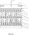
- Figures 3A-3D illustrate alternative embodiments of flexible, two-layer liquid crystal cells which are elastic in the sense described above. These alternative embodiments can be made using materials discussed above with respect to Figure 2 .
- the cell includes a first liquid crystal layer 45 and a second liquid crystal layer 48.
- the first liquid crystal layer 45 is disposed in a gap between an upper (first) liquid crystal polymeric layer 44 and an intermediate (second) liquid crystal polymeric layer 47.
- the second liquid crystal layer 48 is disposed in a gap between the intermediate liquid crystal polymeric layer 47, and a lower (third) liquid crystal polymeric layer 50.
- the upper polymeric layer 44 has directors on the lower surface adjacent the liquid crystal layer 45 that are parallel to the surface of the liquid crystal layer 45, and orthogonal to the plane of the illustration.
- the intermediate polymeric layer 47 has directors on the upper surface adjacent to the liquid crystal layer 45 that are parallel to the surface of liquid crystal layer 45, and orthogonal to the plane of the illustration (i.e., parallel to the directors on the lower surface of the upper polymeric layer 44).
- the intermediate polymeric layer 47 has directors on the lower surface adjacent to the liquid crystal layer 48 that are parallel to the surface of the liquid crystal layer 48, and parallel to the plane of the illustration (i.e. orthogonal to the directors on the upper surface of the intermediate polymeric layer 47).
- Lower polymeric layer 50 has directors on its upper surface adjacent to the liquid crystal layer 48 parallel to the surface of the liquid crystal layer 48 and parallel to the plane of the illustration ( i . e ., parallel to the directors on the lower surface of the intermediate polymeric layer 47).
- the polymeric layers 44, 47, 50 act as alignment layers for the liquid crystal layers.
- the intermediate polymeric layer 47 has orthogonal directors on its upper and lower surfaces.
- the upper and lower polymeric layers 44, 50 may be replaced in some embodiments by other alignment layer materials, such as a brushed polyimide layer. Utilizing brushed polyimide in the intermediate polymeric layer may not be practical, because of optical losses and other problems.
- the alignment technique between the liquid crystal layers in preferred embodiments involves the use of a liquid crystal polymeric layer with orthogonal directors on its upper and lower surfaces.
- the liquid crystal layers 45 and 48 comprise liquid crystal material confined in the gap, and have identical thicknesses between the polymeric layers, within reasonable manufacturing and optical performance tolerances.
- An array of posts (e.g. 46) is disposed in a gap between the upper polymeric layer 44 and the intermediate polymeric layer 47, and is surrounded by the liquid crystal material in the liquid crystal layer 45.
- the posts in the array extend from the upper polymeric layer 44 to the intermediate polymeric layer 47, tending to maintain the thickness as discussed above.
- a second array of posts (e.g. 49) is disposed in a gap between the intermediate polymeric layer 47 and the lower polymeric layer 50.
- the second array of posts is surrounded by the liquid crystal material in the liquid crystal layer 48 confined in the gap.
- electrical components are disposed in a dielectric polymer substrate, including layers 40, 43, 52.
- Electrical components include a resistive layer 41, a patterned electrode layer 42 disposed over the upper polymeric layer 44, and a transparent pad electrode layer 51 below the lower polymeric layer 50.
- the liquid crystal cell of Figure 3A can maintain its optical properties after having been folded over a small radius, and returned to the original shape.
- the two-layer liquid crystal cell can provide a positive lens power for unpolarized light, when an electric field is applied through patterned electrodes.
- the added lens power by the liquid crystal layers is tunable by changing one or more of the amplitude, frequency, duty cycle, DC offset, or pulse shape of the applied electric field.
- Figures 3B through 3D illustrate alternative configurations of two-layer liquid crystal cells like that of Figure 3A .
- the same reference numerals are utilized to refer to like components, which are not described again in some instances.
- the liquid crystal cells of Figures 3B-3D can likewise maintain their optical properties after having been folded over a small radius, and returned to the original shape.
- a polyimide layer can be used with the resistive layer to improve its uniformity.
- the two-layer liquid crystal cell is modified by adding a polyimide layer 60 in contact with the resistive layer 41.
- FIG 3C an embodiment is illustrated in which the two-layer liquid crystal cell is modified by the addition of the polyimide layer 60 in contact with the resistive layer 41, and by moving the upper patterned electrode layer 42 into contact with the upper surface of the upper polymeric layer 44, thereby eliminating the region of layer 43 of the dielectric substrate that is shown in Figures 3A and 3B .
- This has the effect of decreasing the required operating voltage and total thickness of the flexible liquid crystal cell.
- FIG 3D an embodiment is illustrated in which the two-layer liquid crystal cell is modified relative to the structure of Figure 3A , by moving the resistive layer 41 into contact with the upper surface of the upper polymeric layer 44, eliminating much of the region of layer 43 of the dielectric substrate, and eliminating the polyimide layer of Figure 3B and Figure 3C . This further reduces the overall thickness of the structure, and eliminates the requirement for the polyimide layer.
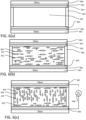
- FIG. 4(a) illustrates an empty process cell as a first illustrated stage in the process.
- the empty process cell consists of upper and lower glass layers 80, 82 which act as cover layers during the forming of the cell.
- the glass layers are coated with the substrate dielectric material 70, 72, 79, the electrode material 71, 78, the resistive layer 73, and the alignment layers, which in this example are polymeric layers 74, 77 as discussed above.
- the upper electrode material 71 is patterned to define a hole used to induce a variable electric field as discussed above to provide for a tunable lens power.
- the lower electrode material 78 is disposed in a pad shape.
- a Mylar film spacer 75 is disposed between the upper polymeric layer 74 and the lower polymeric layer 77 to define a gap 76 in which the liquid crystal layer and the array of posts is to be formed.
- the Mylar film spacer 75 defines a gap thickness of 35 ⁇ m.
- a combination of the liquid crystal material and polymer precursors is injected into the gap 76, relying on capillary force for example.
- the combination includes liquid crystalline monomer moieties 100, a photo-initiator 101, and liquid crystal moieties 102. More specifically in one example process, a combination consists of nematic LC (LCM-1656), liquid crystalline monomer (RM257), and a photo-initiator (IRG184) at ratio of 99 wt%: 0.5 wt%: 0.5 wt%.
- LCM-1656 can be obtained from LC Matter Corp., (e.g., Orlando, FL, USA; lcmatter.com), RM-257 and IRG-184 can be obtained from Merck or Merck KgaA (Darmstadt, Germany, merckgroup.com).
- the materials chosen preferably result in formation of polymer posts having sufficient stiffness to resist severe deformation, but having good elasticity in order to restore the cell gap in the structure after bending.
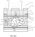
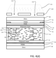
- Figure 4(c) illustrates a next stage in the manufacturing process.
- the cell with the combination material injected into the gap 76, is aligned with the lithographic mask 110 that defines an array of holes 112, 113.
- the structure is then exposed to actinic radiation 111, such as UV radiation in the present example.
- actinic radiation 111 such as UV radiation in the present example.
- the liquid crystal moieties 125 drift away from the regions exposed to the ultraviolet light through the holes 112, 113, while the liquid crystal monomers 120, 121 drift into the region of exposure.
- polymer chains 135 form by photo-polymerization among the liquid crystal monomers 120, 121 to form an array of posts extending between the polymeric layers 74, 77.
- the exposure to actinic radiation 111 can be carried out at low temperature, below 100°C and, in the example being described, near room temperature (about 20-25°C). This low temperature photo-polymerization allows manufacturing without damage to the layers of the structure that are supported by the glass covers during the photo-polymerization process.
- the cell is removed from the lithographic system, with elastic polymer posts extending from an upper surface of the lower polymeric layer 77 to the lower surface of the upper polymeric layer 74, and with liquid crystal filling the gap and surrounding the posts.
- Figure 4(f) illustrates a following stage, in which the glass layers (covers) 80, 82 are removed, leaving the flexible, tunable liquid crystal cell, such as that shown in Figure 2 .
- the liquid crystal cell is sealed by the Mylar spacers in this example using a UV curable polymer.
- the posts are formed in a mixture of liquid crystal and monomers during curing by the photo-polymerization.
- the posts may be formed in a first step, followed by removal of uncured material leaving a network of posts, and then by injection of liquid crystal after the removal around the network of posts.
- the liquid crystal cell can be sealed during the curing by using the patterned mask to define a sealing region, and closing the cell by the same material as used to make the posts.
- This manufacturing process is extendable to the two-layer cell, such as shown in Figures 3A-3D , by adding the intermediate polymeric layer, and a second Mylar spacer to define the second gap. Otherwise, similar processing steps are applied for the two-layer cell.
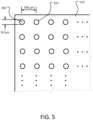
- Figure 5 illustrates a representative layout for the lithographic mask 110, which can be used in the stage of the process described with reference to Figure 4(c) and Figure 4(d) .
- the mask layout comprises an array of circular holes 250, 251 having a diameter of about 50 ⁇ m, and a pitch of about 500 ⁇ m in both the horizontal and vertical dimensions.
- This layout was selected for a liquid crystal layer about 35 ⁇ m thick, using the materials discussed above.
- Other layouts can be chosen according to the needs of a particular embodiment.
- the density of the holes translates into a density of posts that are disposed in the gap between the polymeric layers. The density should be selected so as not to interfere significantly with the electro-optic performance of the cell, while maintaining sufficient elasticity in the sense discussed above so that the shape of the cell returns to its original shape, after having been deformed by folding.
- the holes need not be circular as illustrated in Figure 5 , but can be elliptical, rectangular, or other more complex shapes.
- the preferred shape and density of shapes can be determined using empirical methods or simulation.
- Figures 6(a) to 6(f) illustrate stages of an embodiment of a method for manufacturing the polymeric layers, which are used as alignment layers in the embodiments discussed above.
- Figure 6(a) illustrates a stage of the process including an empty process cell consisting of glass layers 800, 801 coated with respective layers 802, 806 of a conductor such as ITO, and alignment layers 803, 805, such as brushed polyimide, which have been configured to align the directors of the liquid crystal material in the polymeric layer on the opposing surfaces of the polymeric layer according to orientations required for the examples described above.
- a Mylar spacer 804 maintains a gap 810 between the glass layers 800, 801 with a thickness that can be adjusted depending on the design.
- the thicknesses of the upper and lower polymeric layers 24, 27 in Figure 2 are about 7 ⁇ m
- the thickness of the polymeric layer 47 in Figures 3A-3D is about 35 um.
- a mixture of a liquid crystal material including moieties 852, a monomer 851 and a photo-initiator 850 is injected into the empty process cell at a temperature of about 90° C.
- the monomer which can be a mesomer having liquid crystal properties, and liquid crystal are aligned in the mixture according to the direction set by the alignment layers 803, 806.
- the directors in this liquid phase are aligned in the plane of the illustration, and parallel with the plane of the alignment layers 802, 805.
- the conductive ITO layers 802, 806 are connected to a power supply at 900 which applies a high AC voltage which re-orients the molecules of both the monomer (e.g. 856) and the liquid crystal moieties (857) parallel to the z-axis 5 orthogonal to the surfaces of the glass covers.
- the molecular orientations e.g. 854, 855 near the alignment layer surfaces remain parallel to the rubbing directions.
- the structure is exposed to actinic UV radiation 910 while the AC electric field is applied.
- This radiation triggers the photo-initiator and activates the photo-polymerization of the monomer.
- the monomer reacts to form polymer chains, the polymeric films with embedded liquid crystal moieties results between the two glass covers.
- a polymer network e.g. 860 that results from the polymerization traps and helps to maintain the orientation of the liquid crystal molecules in the polymeric layer.
- the electric field and UV radiation can be removed. Then, as shown in Figure 6(f) , the glass covers 802, 801, along with the ITO and alignment layers (802, 803 and 805, 806) are peeled off of the polymeric layer 1000.
- the polymeric layer in this example can be optically anisotropic since the directors of the liquid crystal moieties through the majority of the polymeric layer in the center away from the surfaces in contact with the alignment layers lie on the z-axis.
- the liquid crystal molecules on the surface of the polymeric layers remain disposed parallel to the surfaces of the alignment layer and confined by the polymer networks.
- the surface of the polymeric layer can be used to align liquid crystal molecules in the liquid crystal layer in the structures described above.
- This process can be used to set different orientations of the liquid crystal molecules on the surface of the polymeric layers, by changing the rubbing directions and materials of the alignment layers 803, 805 during fabrication. Also, by applying variable electric fields during polymerization, the alignment direction throughout the polymeric layer can be caused to tilt, resulting in a passive lens effect.
- RM257 is 1,4-Bis-[4-(3-acryloyloxypropyloxy)benzoyloxy]-2-methylbenzene with the CAS 174063-87-7 .
- IRG184 is 1-Hydroxycyclohexyl phenyl ketone with the CAS 947-19-3 .
- the reactive monomer used for the purposes of forming the posts as discussed with reference to Figures 4(a) to 4(f) can be the same ( e . g . RM257) as used as a reactive monomer in the formation of the polymeric layers.
- the polymer precursors can be different in the two procedures.
- different polymer precursors and liquid crystal materials can be used for different polymeric layers in some embodiments.
- the materials for fabricating polymeric layers are not limited to RM257, IRG184 and MLC2144.
- Alternative materials can include other liquid crystalline monomers and photo-initiators.
- the liquid crystal (MLC2144) could be replaced by other nematic liquid crystals.
- the ordering of the polymer network on the surfaces of the polymeric alignment layers should be strong.
- the alignment layers 803, 805 utilized in the process of Figures 6(a) to 6(f) are alignment layers with strong anchoring strength, such as Polyimide AL 22620 or Polyimide SE 7492.
- Other techniques for achieving strong ordering on the surfaces of the polymeric alignment layers can be utilized.
- Figure 7 illustrates a flexible single-layer liquid crystal cell formed on a curved substrate.
- the liquid crystal cell includes a liquid crystal layer 325 disposed in a gap between polymeric layer 324 and polymeric layer 327, where the polymeric layers 324 and 327 comprise flexible or elastic polymer mixed with liquid crystal moieties configured to act as alignment layers for the liquid crystal layer 325.
- the polymeric layers 324, 327 have liquid crystal moieties having a vertical director in the central region of the layers, and horizontal directors on the surfaces. In the upper polymeric layer 324 in this example, the directors on the surfaces are horizontal relative to the major surface of the liquid crystal layer 325, and parallel to the plane of the illustration.
- the directors on the upper surface are horizontal relative to the major surface of the liquid crystal layer 325, and parallel to the plane of the illustration.
- the directors on the lower surface of the lower polymeric layers 327 are parallel to those on the upper surface.
- the orientations of the directors in this example result in the alignment directions on the upper and lower surfaces of the liquid crystal layer 25 parallel to one another.
- An array of posts ( e . g . post 326) is disposed in the liquid crystal layer 325.
- the posts in the array extend from the upper polymeric layer 324 to the lower polymeric layer 327, and tend to maintain the thickness of the liquid crystal layer 325.
- the posts and the polymeric layers comprise an elastic polymer or elastomer.
- the liquid crystal is confined in the gap between the first and second polymeric layers around the posts in the array of posts.
- electrical components are disposed in a dielectric polymer (including layers 320, 322, 329 in this example).
- the electrical components include a resistive layer 323, a patterned electrode layer 321 over the upper polymeric layer 324, and pad electrode layer 328 below the lower polymeric layer 327.
- the substrate of the liquid crystal cell includes the dielectric layers 20, 22 comprising PDMS.
- the radius of curvature of the cell can range in various embodiments from about 100 mm to 8 mm or less.
- the radius of curvature can range from 100 mm to 1 mm.
- Embodiments of the liquid crystal cell shown in Figure 7 can maintain optical properties after having been folded over a small radius, and returned to the original shape.
- Figure 8 illustrates a flexible two-layer liquid crystal cell formed on a curved substrate.
- the cell includes a first liquid crystal layer 425 and a second liquid crystal layer 428.
- the first liquid crystal layer 425 is disposed in a gap between an upper (first) liquid crystal polymeric layer 424 and an intermediate (second) liquid crystal polymeric layer 427.
- the second liquid crystal layer 428 is disposed in a gap between the intermediate liquid crystal polymeric layer 427, and a lower (third) liquid crystal polymeric layer 430.
- the upper polymeric layer 424 has directors on the lower surface adjacent the liquid crystal layer 425 that are orthogonal to the z-axis 5 of the cell, and parallel to the plane of the illustration.
- the intermediate polymeric layer 427 has directors on the upper surface adjacent to the liquid crystal layer 425 that are orthogonal to the z-axis 5, and parallel to the plane of the illustration (i.e. parallel to the directors on the lower surface of the upper polymeric layer 424).
- the intermediate polymeric layer 427 has directors on the lower surface adjacent to the liquid crystal layer 428 that are orthogonal to the z-axis 5, and orthogonal to the plane of the illustration (i.e. orthogonal to the directors on the upper surface of the intermediate polymeric layer 427).
- Lower polymeric layer 430 has directors on its upper surface adjacent to the liquid crystal layer 428 orthogonal to the z-axis 5 and orthogonal to the plane of the illustration (i.e. parallel to the directors on the lower surface of the intermediate polymeric layer 427).
- the polymeric layers 424, 427, 430 act as alignment layers for the liquid crystal layers.
- the intermediate polymeric layer 427 has orthogonal directors on its upper and lower surfaces.
- the upper and lower polymeric layers 424, 430 may be replaced in some embodiments by other alignment layer materials, such as a brushed polyimide layer.
- An array of posts (e.g. 426) is disposed in a gap between the upper polymeric layer 424 and the intermediate polymeric layer 427, and is surrounded by the liquid crystal material in the liquid crystal layer 425 confined in the gap.
- the posts in the array extend from the upper polymeric layer 424 to the intermediate polymeric layer 427, tending to maintain the thickness as discussed above.
- a second array of posts (e.g. 429) is disposed in a gap between the intermediate polymeric layer 427 and the lower polymeric layer 430.
- the second array of posts is surrounded by the liquid crystal material in the liquid crystal layer 428 confined in the gap.
- electrical components are disposed in a dielectric polymer substrate, including layers 432, 433, 434.
- Electrical components include a resistive layer 423, a patterned electrode 421 disposed over the upper polymeric layer 424, and a pad electrode layer 431 below the lower polymeric layer 430.
- the curved embodiments of Figures 7 and 8 can provide passive, additive lens power to the electroactive component of the cell.
- Embodiments of the liquid crystal cells shown in Figures 7 and 8 can maintain optical properties after having been folded over a small radius, and returned to the original shape.
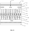
- Figure 9 illustrates another embodiment of a two-layer liquid crystal cell utilizing hybrid alignment of the liquid crystal molecules in the liquid crystal layers.
- the cell includes a first liquid crystal layer 505 and a second liquid crystal layer 508.
- the first liquid crystal layer 505 is disposed in a gap between an upper vertical alignment layer 504, which can comprise PDMS for example, and an intermediate polymeric layer 507.
- the second liquid crystal layer 508 is disposed in a gap between the intermediate polymeric layer 507, and a lower vertical alignment layer 510.
- the intermediate polymeric layer 507 has directors on the upper surface adjacent to the liquid crystal layer 505 that are orthogonal to the z-axis 5 (parallel to the surface of liquid crystal layer 505), and orthogonal to the plane of the illustration.
- the intermediate polymeric layer 507 has directors on the lower surface adjacent to the liquid crystal layer 508 that are orthogonal to the z-axis 5, and parallel to the plane of the illustration (i.e. orthogonal to the directors on the upper surface of the intermediate polymeric layer 507).
- the directors in the liquid crystal layers 505, 508 adjacent to the upper vertical alignment layer 504 and the lower vertical alignment layer 510 are arranged vertically, parallel to the z-axis 5, in the plane of the illustration.
- the directors in the liquid crystal layers twist between the upper and lower surfaces of liquid crystal layers 505, 508 as illustrated, in orthogonal planes because of the alignment function of the intermediate polymeric layer 507.
- the liquid crystal layers 505 and 508 have identical thickness between the polymeric layers, within reasonable manufacturing and optical performance tolerances.
- An array of posts (e.g. 506) is disposed in a gap between the upper alignment layer 504 and the intermediate polymeric layer 507, and is surrounded by the liquid crystal material in the liquid crystal layer 505 confined in the gap.
- the posts in the array extend from the upper alignment layer 504 to the intermediate polymeric layer 507, tending to maintain the thickness as discussed above.
- a second array of posts (e.g. 509) is disposed in a gap between the intermediate polymeric layer 507 and the lower alignment layer 510.
- the second array of posts is surrounded by the liquid crystal material in the liquid crystal layer 508 confined in the gap.
- electrical components are disposed in a dielectric polymer substrate, including layers 512, 510 500, 504.
- Electrical components include a resistive layer 502, a polyimide layer 501, a patterned electrode layer 503 disposed over the upper alignment layer 504, and a pad electrode layer 511 below the lower alignment layer 510.
- the response time can be faster than that of the structure described with reference to Figures 3A-3D .
- the tunable range may be lesser.
- Figure 10 illustrates an alternative embodiment like that of Figure 9 , and the same reference numbers are used to refer to the same components, and not described again.
- the position of the patterned electrode 523 and the resistive film 521/ polyimide film 522 structures are reversed, so that the patterned electrode 523 overlies the resistive film 521. Otherwise the structures are similar, and can behave in similar fashions.
- the liquid crystal cells of Figure 9 and Figure 10 can maintain their optical properties after having been folded over a small radius, and returned to the original shape.
- a patterned electrode may not be utilized.
- a non-uniform electric field can be generated by a pair of transparent pad-shaped electrodes with the addition of dielectric layers having spatially distributed dielectric constants or surfaces into the structure.
- Figure 11 illustrates one embodiment of the structure having transparent electrodes 601 and 610 without electrode patterning.
- the cell shown in Figure 11 includes a first liquid crystal layer 604 and the second liquid crystal layer 607.
- the first liquid crystal layer 604 is disposed in a gap between an upper (first) liquid crystal polymeric layer 603 and an intermediate (second) liquid crystal polymeric layer 606.
- the second liquid crystal layer 607 is disposed in a gap between the intermediate liquid crystal polymeric layer 606 and a lower (third) liquid crystal polymeric layer 609.
- the upper polymeric layer 603 has directors on the lower surface adjacent the liquid crystal layer 604 that are orthogonal to the z-axis 5 (parallel to the surface of liquid crystal layer 604) and orthogonal to the plane of the illustration.
- the intermediate polymeric layer 606 has directors on the upper surface adjacent to the liquid crystal layer 604 that are orthogonal to the z-axis 5 (parallel to the surface of liquid crystal layer 604), and orthogonal to the plane of the illustration (i.e. parallel to the directors on the lower surface of the upper polymeric layer 603).
- the intermediate polymeric layer 606 has directors on the lower surface adjacent to the liquid crystal layer 607 that are orthogonal to the z-axis 5 (parallel to the surface of liquid crystal layer 607), and parallel to the plane of the illustration (i.e. orthogonal to the directors on the upper surface of the intermediate polymeric layer 606).
- Lower polymeric layer 609 has directors on its upper surface adjacent to the liquid crystal layer 607 that are orthogonal to the z-axis 5 (parallel to the surface of liquid crystal layer 607) and parallel to the plane of the illustration (i.e. parallel to the directors on the lower surface of the intermediate polymeric layer 606).
- the liquid crystal layers 604 and 607 have identical thickness between the polymeric layers, within reasonable manufacturing and optical performance tolerances.
- An array of posts (e.g. 605) is disposed in a gap between the upper polymeric layer 603 and the intermediate polymeric layer 606, and is surrounded by the liquid crystal material in the liquid crystal layer 604 confined in the gap.
- the posts in the array extend from the upper polymeric layer 603 to the intermediate polymeric layer 606, tending to maintain the thickness as discussed above.
- a second array of posts (e.g. 608) is disposed in a gap between the intermediate polymeric layer 606 and the lower polymeric layer 609.
- the second array of posts is surrounded by the liquid crystal material in the liquid crystal layer 607 confined in the gap.
- electrical components are disposed in a dielectric polymer substrate, including layers 600, 602, 611 electrical components include flat transparent electrodes 601 disposed over the upper polymeric layer 603, and flat transparent electrodes 610 below the lower polymeric layer 609.
- the polymeric layers 603, 606, 609 act as alignment layers for the liquid crystal layers.
- the intermediate polymeric layer 606 has orthogonal directors on its upper and lower surfaces In this example, the upper surface 603A of the upper polymeric layer 603 is curved, along with a matching curve of the dielectric material in layer 602. The curve can result in generation of a non-uniform electric field when a voltage is applied on the flat transparent electrodes 601 and 610.
- the liquid crystal cell of Figure 11 can maintain its optical properties after having been folded over a small radius, and returned to the original shape.
- Figure 12 illustrates another embodiment in which flat transparent electrodes are used rather than patterned electrodes.
- a two-layer liquid crystal cell utilizing hybrid alignment of the liquid crystal molecules in the liquid crystal layers is illustrated.
- the cell in Figure 12 includes a first liquid crystal layer 704 and a second liquid crystal layer 707.
- the first liquid crystal layer 704 is disposed in a gap between an upper vertical alignment layer 703, which can comprise PDMS for example, and an intermediate polymeric layer 706.
- the second liquid crystal layer is disposed in a gap between the intermediate polymeric layer 706, and a lower vertical alignment layer 709.
- the intermediate polymeric layer 706 has directors on the upper surface adjacent to the liquid crystal layer 704 that are orthogonal to the z-axis 5 (parallel to the surface of liquid crystal layer 704), and orthogonal to the plane of the illustration.
- the intermediate polymeric layer 706 has directors on the lower surface adjacent to the liquid crystal layer 707 that are orthogonal to the z-axis 5 (parallel to the surface of liquid crystal layer 707), and lie in the plane of the illustration (i.e. orthogonal to the directors on the upper surface of the intermediate polymeric layer 706).
- a curved polymeric layer 702 is disposed over and in contact with the upper alignment layer 703. This forms a curved surface 703A in the path of the electric field between the flat transparent electrodes 701 and 710.
- the PDMS layers act as vertical alignment layers 703, 709 for the structure.
- the directors in the liquid crystal layers 704, 707 adjacent to the upper vertical alignment layer 703 and the lower vertical alignment layer 709 are arranged vertically, along the optical path.
- the directors in the liquid crystal layers twist in orthogonal planes between the upper and lower surfaces as illustrated, because of the alignment function of the intermediate polymeric layer 706.
- the liquid crystal layers 704 and 707 have identical thickness between the polymeric layers, within reasonable manufacturing and optical performance tolerances.
- An array of posts (e.g. 705) is disposed in a gap between the upper alignment layer 703 and the intermediate polymeric layer 706, and is surrounded by the liquid crystal material in the liquid crystal layer 704 confined in the gap.
- the posts in the array extend from the upper alignment layer 703 to the intermediate polymeric layer 706, tending to maintain the thickness as discussed above.
- a second array of posts ( e . g . 708) is disposed in a gap between the intermediate polymeric layer 706 and the lower alignment layer 709.
- the second array of posts is surrounded by the liquid crystal material in the liquid crystal layer 707 confined in the gap.
- electrical components include a flat transparent electrode layer 701 disposed over the curved polymeric layer 702, and a flat transparent electrode layer 710 below the lower alignment layer 709.
- Dielectric substrate layers 700, 711 are disposed on the opposing surfaces of the cell.
- the liquid crystal cell of Figure 12 can maintain its optical properties after having been folded over a small radius, and returned to the original shape.
- the orientation of the liquid crystal molecules in the liquid crystal and polymer films can be defined by an external electric field applied during the photo-polymerization.
- the resulting liquid crystal polymer film can have a fixed lens power.
- Using the lens power of liquid crystal polymer lenses in combination with the flexible electroactive components can add lens power to the structure.
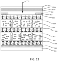
- FIG. 13 An example two-layer liquid crystal electroactive cell, with lens power added by the liquid crystal polymeric layers is shown in Figure 13 .
- the cell includes a first liquid crystal layer 954 and a second liquid crystal layer 957.
- the first liquid crystal layer 954 is disposed in a gap between an upper (first) liquid crystal polymeric layer 953 and an intermediate (second) liquid crystal polymeric layer 956.
- the second liquid crystal layer 957 is disposed in a gap between the intermediate liquid crystal polymeric layer 956, and a lower (third) liquid crystal polymeric layer 959.
- the upper polymeric layer 953 has directors between its surfaces distributed to induce lens power, and has directors on its upper and lower surfaces that are orthogonal to the z-axis 5 (parallel to the surface of liquid crystal layer 954), and orthogonal to the plane of the illustration.
- the directors between the surfaces of the upper polymeric layer 953 tilt by amounts that are a function of their location relative to center line of the optical zone, in planes parallel to the z-axis 5, and orthogonal to the plane of the illustration in this example.
- the intermediate polymeric layer 956 has directors on the upper surface adjacent to the liquid crystal layer 954 that are orthogonal to the z-axis 5 (parallel to the surface of liquid crystal layer 954), and orthogonal to the plane of the illustration (i.e. parallel to the directors on the lower surface of the upper polymeric layer 953).
- the intermediate polymeric layer 956 has directors on the lower surface adjacent to the liquid crystal layer 957 that are orthogonal to the z-axis 5 (parallel to the surface of liquid crystal layer 957), and parallel to the plane of the illustration (i.e. orthogonal to the directors on the upper surface of the intermediate polymeric layer 956).
- the directors between the surfaces and the intermediate polymeric layer 956 are arranged vertically.
- Lower polymeric layer 959 has directors between its surfaces distributed to induce lens power, and has directors on its upper and lower surfaces that are orthogonal to the z-axis 5 (parallel to the surface of liquid crystal layer 957) and parallel to the plane of the illustration (i.e. parallel to the directors on the lower surface of the intermediate polymeric layer 956).
- the directors between the surfaces of the lower polymeric layer 959 tilt by amounts that are a function of their location relative to center line of the optical zone, in planes parallel to the z-axis 5, and parallel to the plane of the illustration in this example.
- the orientations of the directors between the surfaces in the upper and lower polymeric layers are orthogonal to one another.
- the polymeric layers 953, 956, 959 act as alignment layers for the liquid crystal layers.
- the liquid crystal layers 954 and 957 have identical thickness between the polymeric layers, within reasonable manufacturing and optical performance tolerances.
- An array of posts (e.g. 955) is disposed in a gap between the upper polymeric layer 953 and the intermediate polymeric layer 956, and is surrounded by the liquid crystal material in the liquid crystal layer 954 confined in the gap.
- the posts in the array extend from the upper polymeric layer 953 to the intermediate polymeric layer 956, and tend to maintain the thickness as discussed above.
- a second array of posts ( e . g . 958) is disposed in a gap between the intermediate polymeric layer 956 and the lower polymeric layer 959.
- the second array of posts is surrounded by the liquid crystal material in the liquid crystal layer 957 confined in the gap.
- electrical components are disposed in a dielectric polymer substrate, including layers 950, 961, 962.
- Electrical components include a resistive layer 951B, with the contacting polyimide layer 951A, a patterned electrode layer 952 disposed over the upper polymeric layer 953, and a transparent pad electrode layer 960 below the lower polymeric layer 959.
- the distributed directors in the upper polymeric layer 953 and the lower polymeric layer 959 provide added lens power to the electroactive cell.
- the passive lens power provided by the polymeric layers 953 and 959 can be combined with electroactive power provided by the liquid crystal layers to enable utilization of the lens structure to focus on near objects and on far objects.
- the liquid crystal cell of Figure 13 can maintain its optical properties after having been folded over a small radius, and returned to the original shape.
- Figure 14 illustrates an embodiment of a tunable electroactive liquid crystal cell for a lens in which the two-layer liquid crystal cell is modified relative to the structure of Figure 3D , by removing the pad electrode layer 51 below the second liquid crystal layer 48, and providing a second electrode 42A having a patterned opening.
- the second electrode 42A is disposed in a dielectric polymer 40A.
- a resistive layer 41A is disposed below the alignment layer 50.
- the patterned openings in the first electrode 42 and the second electrode 42A can have circular shapes. In some embodiments, the patterned openings have circular shapes with a common radius. In other embodiments, the patterned openings can have circular shapes with different radii. Also, in other embodiments, the patterned openings can have shapes other than circular.
- the circular openings in the embodiment of Figure 14 are disposed in alignment with an aperture of the tunable lens, configured to induce electric field lines, with electric field power, suitable for controlling the alignment of the liquid crystal moieties in the first and second active layers to achieve a tunable lens power.
- first and second electrodes 42 and 42A having hole patterned openings which can be replaced using pad electrodes and curved polymeric layers as in the case of Figures 11 and 12 .
- passive lens power can be provided using polymeric layers as discussed above.
- Figure 15 illustrates an embodiment of a tunable electroactive liquid crystal cell for a lens in which the two-layer liquid crystal cell is modified relative to the structure of Figure 14 , by inserting a pad electrode 150 between the first and second active layers containing liquid crystal ( i . e ., liquid crystal layers 45, 48).
- a pad electrode 150 between the first and second active layers containing liquid crystal (i . e ., liquid crystal layers 45, 48).
- Elements of Figure 15 in common with the embodiment of Figure 14 have like reference numbers and are not described again.
- a transparent flexible pad electrode 150 is disposed in a dielectric polymer 155, 156 below the second alignment layer 47.
- An additional alignment layer 47A is disposed below the pad electrode 150 and in contact with an upper surface of the second liquid crystal layer 48.
- the first and second electrodes 42, 42A can have patterned openings as discussed above in connection with Figure 14 .
- a driver including a first drive signal source 160 and a second drive signal source 161 is electrically connected to the first patterned electrode 42 and second patterned electrode 42A to apply a first drive signal for the first liquid crystal layer 45 and a second drive signal for the second liquid crystal layer 48.
- the first and second drive signals can be the same, within manufacturing and performance specifications.
- the first and second drive signals can differ in at least one of, and in some embodiments more than one of, pulse shape, duty cycle, DC offset, amplitude, and frequency. Characteristics of the drive signals can be determined, for example, by calibration for particular lens powers, and other performance characteristics to be achieved.
- the driver is coupled to the pad electrode 150, and applies a DC reference voltage or ground to the pad electrode.
- the first drive signal can be coupled between the first electrode and the first pad electrode, and the second drive signal can be coupled between the second electrode and the second pad electrode.
- Figure 16 illustrates an embodiment of a tunable electroactive liquid crystal cell for a lens in which a curved two-layer liquid crystal cell is modified relative to the structure of Figure 8 , by inserting a pad electrode 450 between the first and second active layers (425, 428), and also by replacing the pad electrode of Figure 8 with a second electrode 421A having a patterned opening such as electrode 42A discussed with reference to Figures 14 and 15 .
- Elements of Figure 16 in common with the structure of Figure 8 have like reference numbers and are not described again.
- a transparent flexible pad electrode 450 is disposed in a dielectric polymer 455, 456 below the second alignment layer (polymeric layer 427).
- An additional alignment layer is disposed below the pad electrode 450 and in contact with an upper surface of the second liquid crystal layer 428.
- the second electrode 421A is disposed in a dielectric polymer 433A, 434A. Also a resistive layer 423A is disposed below the polymeric layer 430.
- a driver including a first drive signal source 460 and a second drive signal source 461 is electrically connected to the first patterned electrode 421 and second patterned electrode 421A to apply a first drive signal for the first liquid crystal layer 425 and a second drive signal for the second liquid crystal layer 428.
- the first and second drive signals can be the same, within manufacturing and performance specifications.
- the first and second drive signals can differ in at least one of, and in some embodiments more than one of, pulse shape, duty cycle, DC offset, amplitude and frequency. Characteristics of the drive signals can be determined for example by calibration for particular lens powers, and other performance characteristics to be achieved.
- the driver is coupled to the pad electrode 450, and applies a DC reference voltage or ground to the pad electrode.
- the first drive signal can be coupled between the first electrode and the first pad electrode, and the second drive signal can be coupled between the second electrode and the second pad electrode.
- the disclination effect can be reduced by using alignment layers with strong anchoring strength, such as alignment layers having an anchoring strength greater than 10 -4 J/m 2 .
- An alignment layer having sufficient strength can be manufactured as discussed above using polymeric alignment layers.
- Figure 17 is a graph showing a drive signal having a duty cycle that is not equal to 50%.
- the drive signal is an AC square wave in which the magnitude of the positive and negative peaks is equal.
- the pulse width ⁇ of the positive going pulse is less than 50% of the period T of the signal.
- the drive signal can be a sinusoidal wave, a sawtooth wave, or other signal having different pulse shapes or mixed pulse shapes.
- Figure 18 is a graph showing a drive signal in which the magnitudes of the positive and negative peaks are not equal, inducing a DC offset.
- the duty cycle of the drive signal is 50%.
- drive signals can be applied that have a combination of adjustable duty cycle, and adjustable magnitudes of the positive and negative peaks.
- the drive signals can be applied using pulse width modulation in order to achieve desired lens power characteristics.
- the pulse width modulation can be applied using feedback indicating a quality of focus, for example at the selected lens power, in order to control for environmental factors in real time.
- Lens power of a liquid crystal lens is different under positive voltage or negative voltage due to the ion effect or the flexoelectric effect.
- Altering pulse width can provide an average voltage with a positive DC offset or a negative DC offset and thus change the lens power.
- the frequency and magnitude determine the electric field strength in the liquid crystal layer that is applied to the adjustment of the directors in the liquid crystal moieties.
- FIG 19 is a simplified illustration, for the purposes of discussion, of a tunable liquid crystal cell having a first electrode 480 with a patterned opening, the resistive layer 481 to assist dispersion of the electric field lines, and a second electrode 482, such as a pad electrode.
- the liquid crystal layer is disposed between the first electrode 480 and the second electrode 482.
- the liquid crystal layer includes liquid crystal, having moieties ( e . g . 485) aligned according to alignment layers (not shown) in the cell with an applied bias in a passive state for example.
- the alignment layers can comprise polymeric alignment layers as discussed in detailed above.
- the liquid crystal cell can include elastic posts as described above.
- the liquid crystal cell can be combined with an additional cell as discussed above.
- Figure 20 illustrates the liquid crystal cell of Figure 19 with an applied initial drive signal inducing a relatively high power electric field represented by the field lines extending in a dispersed pattern from the first electrode 480 to the second electrode 482.
- the liquid crystal moieties in the liquid crystal layer can become substantially uniformly vertically aligned.
- a drive signal as represented by Figure 21 is applied having a lower power electric field represented by the field lines extending in a dispersed pattern from the first electrode 480 to the second electrode 482 in Figure 21 .
- the drive signal of Figure 21 is applied subsequent to the initial drive signal, and allows the liquid crystal moieties to relax into the desired orientation for the target lens power.
- Figure 22 is a graph showing a drive signal having an initial higher power interval, followed by a subsequent lower power interval as discussed with reference to Figures 21 and 22 .
- the drive signal has a first frequency f1 and a first magnitude V1 to establish a relatively uniform electric field distribution, as in Figure 20 .
- the drive signal has a second frequency f2 and a second magnitude V2 to set a lens power as in Figure 21 .
- Combination of frequency and magnitude establishes an electric field power that can cause controllable alignment of the liquid crystal moieties in the active layer, and can be usable to adjust the lens power in the liquid crystal layer of the cell more quickly with less disinclination on the perimeter of the lens field.
- the drive signal in the initial higher field power interval can have a lower frequency f1 and a higher magnitude V1 than the frequency f2 and magnitude V2 of the drive signal in the subsequent lower field power interval.
- the initial higher power interval can be a single high magnitude pulse, rather than a set of multiple cycles.
- Other combinations of frequency and magnitude, and drive signals including DC offsets, adjustable duty cycles, and pulse width modulation can be applied as well in various combinations to achieve the initial and subsequent field powers for a particular implementation.
- f1, V1 can be 500 Hz, 40Vrms for 500 milliseconds
- f2 can be 4KHz, 35 Vrms.
- the flexible liquid crystal cell technology described is suitable for use in flexible lenses, such as contact lenses, which can be elastic in the sense that the structure will return to its original shape and original optical properties after having been folded.
- Embodiments of flexible liquid crystal cells can include optics that are all polymer based.
- the liquid crystal cell can include a polarizer or be polarizer-free.
- the technology described for manufacturing an array of posts within a liquid crystal layer is based on photo-polymerization at low temperature of a mixture including polymer precursors and liquid crystal material.
- the photo-polymerization induces a phase separation and polymerization of the precursors to form the array of posts, according to a pattern formed using a lithographic mask for example.
- Flexible liquid crystal cells described herein can be folded on themselves without breaking, and can be returned to the original shape while recovering optical properties of the electroactive lens.
- the thickness of the liquid crystal layers can be maintained before and after folding, such that the average thickness before and after folding remains within 10% of the initial thickness.
- the thickness of the liquid crystal layers can be a uniform thickness before and after folding, varying for example by less than 1.2 ⁇ m from the center of the optic to the edge of the effective aperture of the optic.
- the technology is described for implementing flexible optical elements that use liquid crystals to realize electrically tunable optics.
- the liquid crystal optics can include a pair of liquid crystal layers with orthogonally aligned liquid crystal directors to enable polarizer-free operation, with flexible polymeric alignment layers, flexible substrates and a module for controlling the electric field.
- Lens power of the liquid crystal optics can be changed by controlling the distribution of the electric field across the entire optical zone.
- a flexible contact lens can be implemented using the technology described herein with a negative lens power for the purposes of focusing on far objects, and an additive lens power for the purposes focusing on near objects.
- the negative lens power can be provided by passive structure of the stack of optical layers, combined with the electro-optic active structure of the liquid crystal layers.
- a flexible contact lens can include a flexible optical element that uses liquid crystals, as described herein.
- the LC optics can include a pair of LCs layered with orthogonally aligned LC directors for polarizer-free operation, flexible polymeric alignment layers, flexible substrates, and a module for controlling the electric field.
- the lens power of the LC optics can be changed by controlling the distribution of electric field across the optical zone.
- the liquid crystal cells as described herein can be included in a contact lens that comprises a flexible polymer.
- a flexible contact lens For patients with myopia and presbyopia, or hyperopia and presbyopia, simultaneously, a flexible contact lens is described with negative lens power to support focus on far objects and an added positive lens power to support focus on near objects.
- the LC optics can provide the added positive lens power electrically and can be combined with the flexible contact lens with passive, initial negative lens power for those patients.
Landscapes
- Physics & Mathematics (AREA)
- Nonlinear Science (AREA)
- General Physics & Mathematics (AREA)
- Optics & Photonics (AREA)
- Chemical & Material Sciences (AREA)
- Crystallography & Structural Chemistry (AREA)
- Ophthalmology & Optometry (AREA)
- Health & Medical Sciences (AREA)
- Mathematical Physics (AREA)
- General Health & Medical Sciences (AREA)
- Spectroscopy & Molecular Physics (AREA)
- Geometry (AREA)
- Liquid Crystal (AREA)
- Eyeglasses (AREA)
Description
- The present invention relates to electroactive optics and lenses using such optics and, in particular, to flexible liquid crystal cells and lenses.
- As soft contact lenses are handled by contact lens wearers, they are subject to deformation. In some cases, the lenses may be folded in half over short folding radii, as small as 2 millimeters or so. Thus, the soft contact lens should be flexible enough to endure this deformation without damage over reasonable useable lifetime. It is desirable also that the lens be elastic in the sense that it is capable of recovering its size and shape and of retaining the optical properties of the lens after recovering from the deformation. A number of polymers, including hydrogel contact lenses and silicone hydrogel contact lenses, have been developed with flexibility and elasticity in mind.
- In electroactive lenses, the electroactive components, such as liquid crystal cells, can be embedded in a lens body made of a flexible and elastic polymer. However, electroactive components can limit both the flexibility and the elasticity of the lens body as a whole.
WO2012/037684 describes a tunable liquid crystal optical device.US7369327 describes a variable optical-property element comprising liquid crystal. The variable optical-property element is capable of changing its optical properties as a liquid crystal lens.EP1291705 describes a compound liquid crystal microlens for a sensor.EP2851743 describes an ophthalmic lens comprising a liquid crystal layer that is used to provide a variable optic function.EP3223066 describes a lens for the purpose of slowing, retarding, controlling or preventing myopia development or progression, correcting presbyopic vision or allowing extended depth of focus.US2007/0268417 describes an automatic focus apparatus in which a predetermined voltage is applied to a liquid crystal lens. - It is desirable to provide a lens with electroactive components that is both flexible and elastic.
- In accordance with the present invention, there is provided a flexible electrically tunable lens in accordance with
claims 1, 12, 13, 14 and 15. The lens comprises first and second alignment layers, with an active layer comprising liquid crystal confined between the first and second alignment layers in an optical path of the lens. A first electrode is disposed above the first alignment layer and may have a first patterned opening, such as a circular hole, disposed over an aperture region of the active layer. Also a second electrode is disposed below the second alignment layer, and may have a second patterned opening arranged to induce, in combination with the first electrode, an electric field in the active layer. The first and second patterned openings can be circular in shape. In some embodiments, the first and second patterned openings have circular shapes with a common radius. In some embodiments, the first and second patterned openings have circular shapes with different radii. - In flexible or elastic versions of the embodiments including first and second electrodes having patterned openings, and in other embodiments described herein, an array of elastic polymer posts is disposed in the active layer, configured to maintain the thickness of the active layer after bending and recovery of its original shape.
- Embodiments of the electrically tunable lens described herein can have resistive layers disposed above the first alignment layer and below the second alignment layer to improve dispersion of the electric field lines through the active layer.
- One or both of the first and second alignment layers comprise a polymeric layer including liquid crystal moieties.
- In some embodiments, a third alignment layer is disposed between the first and second alignment layers, and a second active layer comprising liquid crystal is confined between the third alignment layer and the second alignment layer. A pad electrode can be disposed between the first and second active layers.
- A driver is electrically connected to the first and second electrodes. The driver can be configured to apply a drive signal across the first and second electrodes. In various embodiments, the driver can apply a drive signal having an adjustable duty cycle. The driver can apply a drive signal using pulse width modulation. The driver can apply a drive signal having a DC offset.
- In some embodiments, the driver can apply a drive signal that includes an initial higher field power interval followed by a subsequent lower field power interval, where the lower field power interval is configured to establish a target lens power during the lower field power interval. The combination of the higher field power interval followed by the lower field power interval can reduce disclination of liquid crystal moieties in the active layers, particularly near the edges of the aperture region of the lens.
- In embodiments described herein, at least one of the first and second alignment layers has an anchoring strength greater than 10-4 J/m2. Embodiments are described in which alignment layers comprise polymeric layers including liquid crystal moieties, having an anchoring strength greater than 10-4 J/m2. Polymeric layers of this type can be flexible and can be elastic.
- Also, an electrically tunable lens is described that comprises first, second, third and fourth alignment layers, having a first active layer comprising liquid crystal between the first and second alignment layers, and a second active layer comprising liquid crystal between the third and fourth alignment layers. The first electrode is disposed above the first alignment layer and has a first patterned opening disposed in alignment with an aperture of the first active layer. A second electrode is disposed below the fourth active layer, and has a second patterned opening disposed in alignment with an aperture of the second active layer. A pad electrode is disposed between the first and second active layers. A driver is electrically connected to the first and second electrodes and to the pad electrode. The driver is configured to apply a first drive signal to the first electrode and a second drive signal to the second electrode. The pad electrode can be maintained at a reference potential such as ground, or otherwise used in the generation of the first and second drive signals. The drive signals are arranged to induce, in combination with the pad electrode, electric fields in the first and second active layers to tune the optical power of the lens. Many of the features discussed above can be applied to this type of electrically tunable lens having two active layers, with outer electrodes having patterned openings and an intermediate pad electrode.
- Also, an elastic or flexible, electrically tunable liquid crystal lens is described. The liquid crystal lens includes a cell with a cell gap thickness that is substantially retained after it has been folded and returned to its original shape. Thus, the shape and optical properties of the liquid crystal lens can recover after folding.
- Embodiments described include an electroactive cell comprising a liquid crystal in a gap between polymeric alignment layers, with an array of polymer posts disposed in the gap between the alignment layers.
- In examples described herein, one or more of the alignment layers comprises a flexible polymeric material including embedded liquid crystal moieties.
- Some examples of an electrically tunable lens described herein comprise a first alignment layer and a second alignment layer; an array of elastic polymer posts in a gap between the first alignment layer and the second alignment layer, posts in the array extending from the first alignment layer to the second alignment layer; liquid crystal confined in the gap between the first and second alignment layers around posts in the array; and one or more electrodes arranged to induce an electric field in the liquid crystal.
- A polarization-independent example includes a third alignment layer and a second array of elastomer posts in a second gap between the second alignment layer and the third alignment layer, posts in the second array extending from the second alignment layer to the third alignment layer. Also, liquid crystal is confined in the second gap around posts in the second array. The second alignment layer in the example can include liquid crystal moieties having directors aligned orthogonal to an optical path and parallel near a first surface adjacent to the first mentioned gap, and directors aligned orthogonal to an optical path near a second surface adjacent to the second mentioned gap and orthogonal to the directors near the first surface.
- Methods for manufacturing flexible liquid crystal cells are described, including formation of polymer posts in liquid crystal layers by photo-polymerization according to a pattern. In an embodiment described herein, the method includes assembling a first flexible alignment layer and a second flexible alignment layer with a gap therebetween; forming flexible or elastic polymer posts extending across the gap between the first flexible alignment layer and the second flexible alignment layer; and providing liquid crystal material surrounding the posts in the gap. In embodiments described herein, the method includes providing a combination of a liquid crystal material and a polymer precursor material in the gap, and forming the elastic posts by inducing phase separation of the polymer precursor and liquid crystal, and polymerizing the polymer precursor according to a pattern.
- Various combinations and additions to the devices and methods are described below.
- Other aspects and advantages of the present invention can be seen on review of the drawings, the detailed description and the claims, which follow.
-
-
Figure 1 is a simplified illustration showing folding of a flexible lens with an electroactive cell as described herein. -
Figure 2 illustrates a flexible liquid crystal electroactive cell having a single liquid crystal layer. -
Figures 3A ,3B ,3C and3D illustrate alternative embodiments of a polarization-independent, flexible liquid crystal electroactive cell having two liquid crystal layers. -
Figures 4(a), 4(b) ,4(c) ,4(d) ,4(e) and 4(f) illustrate stages in a manufacturing process for a flexible electroactive cell. -
Figure 5 shows an example layout for a lithographic mask used in processes like that ofFigures 4(a), 4(b) ,4(c) ,4(d) ,4(e) and 4(f) . -
Figures 6(a), 6(b), 6(c) ,6(d), 6(e) and6(f) illustrate stages in the manufacturing of a polymeric layer like that used in the structure ofFigures 2 and3A ,3B ,3C , and3D . -
Figure 7 illustrates an example of a curved, flexible liquid crystal electroactive cell. -
Figure 8 illustrates an example of a curved, flexible liquid crystal electroactive cell having two layers of liquid crystal. -
Figure 9 illustrates an example of a two-layer liquid crystal cell, having hybrid alignment in the liquid crystal layers. -
Figure 10 illustrates an example of a two-layer liquid crystal cell, having hybrid alignment in the liquid crystal layers with an alternative electrode position. -
Figure 11 illustrates an example of a two-layer liquid crystal cell with a curved dielectric layer. -
Figure 12 illustrates another example of a two-layer liquid crystal cell with a curved dielectric layer, with hybrid alignment in the liquid crystal layers. -
Figure 13 illustrates an example of a two-layer liquid crystal cell, with lens power in liquid crystal polymeric films. -
Figure 14 illustrates an example of a two-layer liquid crystal cell, like that ofFigure 3D , but modified so that the upper and lower electrodes both have patterned openings. -
Figure 15 illustrates an example of a two-layer liquid crystal cell, having an intermediate pad electrode, with first and second outer electrodes having patterned openings. -
Figure 16 illustrates an example of a two-layer liquid crystal cell like that ofFigure 15 , which is curved rather than flat. -
Figure 17 is a graph showing a drive signal for a liquid crystal cell having a duty cycle configured to induce a DC offset in the active layer. -
Figure 18 is a graph showing a drive signal for a liquid crystal cell having a DC offset in the drive signal. -
Figure 19 is a simplified diagram of an active layer having liquid crystal moieties disposed between a hole patterned top electrode and a pad electrode in an unbiased state. -
Figure 20 is a simplified diagram of the structure ofFigure 19 with an initial applied drive signal having a relatively high field power inducing a vertical alignment of the liquid crystal moieties. -
Figure 21 is a simplified diagram of the structure ofFigure 19 , with a subsequent applied drive signal having a lower field power than that ofFigure 20 , set to establish a preferred lens power. -
Figure 22 is a graph showing a drive signal including an initial higher field power interval and a subsequent lower field power interval as discussed with reference toFigures 20 and 21 . - A detailed description of embodiments of the present invention is provided with reference to the
Figures 1-22 . -
Figure 1 illustrates alens 10 having anelectroactive cell 11 embedded therein. Thelens 10 is flexible and can comprise a hydrogel material or a silicone hydrogel material for example. Theelectroactive cell 11 includes electroactive material and at least one electronic component that is used to change the refractive power of the lens. As illustrated inFigure 1 , thelens 10 can be folded when it is made of a flexible material as it is handled by the user. For example, when thelens 10 is a contact lens, then the user may fold the lens when inserting and removing it from the eye. When the lens is folded as illustrated in the lower portion of the Figure, the radius R of the fold can be very small particularly inregion 12. For example, a lens can be folded on a fold radius on the order of 1 to 9 mm. When the lens is folded, theelectroactive cell 11 can be deformed. - In embodiments described herein, the electroactive cell is elastic in the sense that it recovers its shape and its tunable or adjustable optical characteristics when returned to its original shape, after it is folded.
-
Figure 2 illustrates a flexible single layer liquid crystal cell which is elastic in the sense described above. The liquid crystal cell includes a liquid crystal layer 25 (i.e., an active layer comprising liquid crystal) disposed in a gap between an upper (first)polymeric layer 24 and a lower (second)polymeric layer 27, where thepolymeric layers liquid crystal layer 25. The polymeric layers 24, 27 have liquid crystal moieties having a vertical director in the central region of the layers, and horizontal directors on the surfaces. In theupper polymeric layer 24 in this example, the directors near the surfaces are orthogonal to the z-axis 5, which can be the optical axis, and horizontal relative to the major surface of theliquid crystal layer 25, extending into and out of the plane of the illustration. In thelower polymeric layer 27 in this example, the directors on the opposing surfaces are horizontal relative to the major surface of theliquid crystal layer 25, extending into and out of the plane of the illustration. The orientations of the directors in this example result in the alignment directions on the upper and lower surfaces of theliquid crystal layer 25 being parallel to one another. - In this example, the
liquid crystal layer 25 has a uniform thickness T between thepolymeric layers - An array of posts (e.g. post 26) is disposed in the gap between the
polymeric layers upper polymeric layer 24 to thelower polymeric layer 27, and tend to maintain the thickness T. The posts (e.g. 26) can comprise a polymer or polymeric material. Preferably the posts are elastic. Also, preferably, the polymeric layers comprise an elastic polymer or elastomer. - Liquid crystal material is confined in the gap between the first and second polymeric layers around the posts in the array of posts, and acts as the active element of the cell, changing the optical characteristics of the cell in response to an applied electric field.
- In this example, electrical components used to apply an electric field in the
liquid crystal layer 25 are disposed in a dielectric polymer (includinglayers resistive layer 23, a circular hole patternedelectrode layer 21 over theupper polymeric layer 24, and transparentpad electrode layer 28 below thelower polymeric layer 27. In this, and in other embodiments described herein, the patterned electrode layer can have patterns other than a circular hole in some embodiments, including pixelated patterns, and ring-shaped patterns, for more complex control of the shape of the electric field vectors in the liquid crystal layer. - In one representative embodiment, the substrate of the liquid crystal cell includes the
dielectric layers dielectric layer 29 likewise comprises PDMS about 17 µm thick or less. The patterned and pad electrode layers 21, 28 can comprise a flexible electrode material about 1 µm thick or less. Theliquid crystal layer 25 can be about 30-40 µm thick, such as about 34 µm thick. The upper and lower polymeric layers can be about 6 to 7 µm thick. In this example, the cell has a total thickness of about 98 µm. - In a further embodiment, the substrate of the liquid crystal cell includes the
dielectric layers dielectric layer 29 can comprise PDMS and have a thickness from 15 µm to 20 µm. The patterned and pad electrode layers 21, 28 can comprise a flexible electrode material having a thickness from 0.1 µm to 1 µm. Theliquid crystal layer 25 can be 25 µm to 45 µm thick. The upper and lower polymer layers can each have a thickness from 5 µm to 10 µm. - In a representative embodiment, the thickness T of the
liquid crystal layer 25 is about 34 µm. - In some embodiments, the thickness T is a constant thickness throughout the optical zone of the
liquid crystal layer 25, where the optical zone is the effective aperture in which the tunable lens effect is utilized. - A uniform thickness for the cell in this example can be a thickness that varies by less than 1.2 microns from the center of the optic to the edge of the effective aperture. In some embodiments, the variation of thickness T within the effective aperture can be maintained within 0.5 micron.
- Embodiments of the liquid crystal cells described herein can maintain optical properties after having been folded over a small radius, and returned to the original shape. For example, in an embodiment comprising a cell gap having an average original thickness T with the liquid crystal layer before folding of about 10 µm, the average thickness T can return to within 10% of its original thickness, or to an average thickness in the range of 9 to 11 µm. In other embodiments, the average thickness T can return to within 2 % of its original thickness, or to an average thickness in the range of 9.8 to 10.2 µm. The average thickness of the cell gap or the liquid crystal layer can be determined by measuring the thickness at multiple locations and adding those measurements together and dividing by the number of measurements. The measurements can be taken along a single diameter of the liquid crystal layer (if it has a circular shape), or they can be taken along random points around the liquid crystal layer.
- Depending on the requirements of particular implementations, the materials of the flexible
dielectric layers
PET (polyethylene terephthalate)-containing materials, and hydroxyethyl methacrylate (HEMA)-containing materials. - Depending on the requirements of particular implementations, representative materials usable for the patterned
electrode layer 21 and for the transparentpad electrode layer 28 can be poly(3,4-ethylenedioxythiophene) polystyrene sulfonate (PEDOT:PSS), indium tin oxide (ITO), indium zinc oxide (IZO), graphene, silver nanowires and copper metal mesh, and combinations of materials. - A function of
resistive layer 23 is to help distribute the electric field into the center of the effective aperture of the lens. Theresistive layer 23 has a relatively high resistance relative to the electrodes, and can be referred to as a highly resistive layer. With theresistive layer 23, the operating voltage can be decreased in some examples. The sheet resistance of a resistive layer can be around 106~108 Ω/sq depending on the lens materials and specifications. The resistive layer can be made by mixing PEDOT:PSS solution and PVA (Poly(vinyl alcohol)) solution. The sheet resistance can be controlled for example by the weight ratio between two solutions. - Liquid crystals (LC) are optical anisotropic materials which have a birefringence property. Consider a linear-polarized light which is normally incident to LC optics and the polarization direction and long axis of LC molecules are in the same plane. The light experiences an effective refractive index which is determined by the angle between polarization-direction of light and the director of LC. In addition, the orientation of LC molecules can be controlled by external electric fields. Therefore, a non-uniform electric field on the LC layer with uniform thickness will cause spatial distribution of the orientation of LC molecules. The spatial distribution of the orientation of LC molecules will also form a spatial distribution of effective optical path. By appropriate design, the spatial distribution of effective optical path can realize the lens effect with different lens powers.
- LCs can be polarization dependent, which can cost at least 50% of light efficiency when used in combination with a polarizer. To realize polarization-independent LC optics, a pair of LC layers with identical thickness and orthogonally aligned LC directors, as implemented in the examples shown in
Figures 3A to 3D , can be used. Using the pair of LC layers with orthogonal directors, two Eigen-polarizations of light experience the same phase shift, resulting in a polarization-independent, tunable lens. -
Figures 3A-3D illustrate alternative embodiments of flexible, two-layer liquid crystal cells which are elastic in the sense described above. These alternative embodiments can be made using materials discussed above with respect toFigure 2 . - In
Figure 3A , the cell includes a firstliquid crystal layer 45 and a secondliquid crystal layer 48. The firstliquid crystal layer 45 is disposed in a gap between an upper (first) liquidcrystal polymeric layer 44 and an intermediate (second) liquidcrystal polymeric layer 47. The secondliquid crystal layer 48 is disposed in a gap between the intermediate liquidcrystal polymeric layer 47, and a lower (third) liquidcrystal polymeric layer 50. - The
upper polymeric layer 44 has directors on the lower surface adjacent theliquid crystal layer 45 that are parallel to the surface of theliquid crystal layer 45, and orthogonal to the plane of the illustration. Theintermediate polymeric layer 47 has directors on the upper surface adjacent to theliquid crystal layer 45 that are parallel to the surface ofliquid crystal layer 45, and orthogonal to the plane of the illustration (i.e., parallel to the directors on the lower surface of the upper polymeric layer 44). Theintermediate polymeric layer 47 has directors on the lower surface adjacent to theliquid crystal layer 48 that are parallel to the surface of theliquid crystal layer 48, and parallel to the plane of the illustration (i.e. orthogonal to the directors on the upper surface of the intermediate polymeric layer 47).Lower polymeric layer 50 has directors on its upper surface adjacent to theliquid crystal layer 48 parallel to the surface of theliquid crystal layer 48 and parallel to the plane of the illustration (i.e., parallel to the directors on the lower surface of the intermediate polymeric layer 47). - The polymeric layers 44, 47, 50 act as alignment layers for the liquid crystal layers. The
intermediate polymeric layer 47 has orthogonal directors on its upper and lower surfaces. The upper and lowerpolymeric layers - The liquid crystal layers 45 and 48 comprise liquid crystal material confined in the gap, and have identical thicknesses between the polymeric layers, within reasonable manufacturing and optical performance tolerances.
- An array of posts (e.g. 46) is disposed in a gap between the
upper polymeric layer 44 and theintermediate polymeric layer 47, and is surrounded by the liquid crystal material in theliquid crystal layer 45. The posts in the array extend from theupper polymeric layer 44 to theintermediate polymeric layer 47, tending to maintain the thickness as discussed above. - A second array of posts (e.g. 49) is disposed in a gap between the
intermediate polymeric layer 47 and thelower polymeric layer 50. The second array of posts is surrounded by the liquid crystal material in theliquid crystal layer 48 confined in the gap. - In this example, electrical components are disposed in a dielectric polymer substrate, including
layers resistive layer 41, a patternedelectrode layer 42 disposed over theupper polymeric layer 44, and a transparentpad electrode layer 51 below thelower polymeric layer 50. - The liquid crystal cell of
Figure 3A can maintain its optical properties after having been folded over a small radius, and returned to the original shape. - In general, the two-layer liquid crystal cell can provide a positive lens power for unpolarized light, when an electric field is applied through patterned electrodes. The added lens power by the liquid crystal layers is tunable by changing one or more of the amplitude, frequency, duty cycle, DC offset, or pulse shape of the applied electric field.
-
Figures 3B through 3D illustrate alternative configurations of two-layer liquid crystal cells like that ofFigure 3A . The same reference numerals are utilized to refer to like components, which are not described again in some instances. The liquid crystal cells ofFigures 3B-3D can likewise maintain their optical properties after having been folded over a small radius, and returned to the original shape. - As shown in
Figure 3B , in alternative configurations, a polyimide layer can be used with the resistive layer to improve its uniformity. Thus, inFigure 3B the two-layer liquid crystal cell is modified by adding apolyimide layer 60 in contact with theresistive layer 41. - In
Figure 3C , an embodiment is illustrated in which the two-layer liquid crystal cell is modified by the addition of thepolyimide layer 60 in contact with theresistive layer 41, and by moving the upperpatterned electrode layer 42 into contact with the upper surface of theupper polymeric layer 44, thereby eliminating the region oflayer 43 of the dielectric substrate that is shown inFigures 3A and3B . This has the effect of decreasing the required operating voltage and total thickness of the flexible liquid crystal cell. - In
Figure 3D , an embodiment is illustrated in which the two-layer liquid crystal cell is modified relative to the structure ofFigure 3A , by moving theresistive layer 41 into contact with the upper surface of theupper polymeric layer 44, eliminating much of the region oflayer 43 of the dielectric substrate, and eliminating the polyimide layer ofFigure 3B andFigure 3C . This further reduces the overall thickness of the structure, and eliminates the requirement for the polyimide layer. - An embodiment of a method for manufacturing flexible liquid crystal cell like that of
Figure 2 is illustrated inFigures 4(a) to Figure 4(f) . -
Figure 4(a) illustrates an empty process cell as a first illustrated stage in the process. The empty process cell consists of upper and lower glass layers 80, 82 which act as cover layers during the forming of the cell. The glass layers are coated with thesubstrate dielectric material electrode material resistive layer 73, and the alignment layers, which in this example arepolymeric layers upper electrode material 71 is patterned to define a hole used to induce a variable electric field as discussed above to provide for a tunable lens power. Thelower electrode material 78 is disposed in a pad shape. AMylar film spacer 75 is disposed between theupper polymeric layer 74 and thelower polymeric layer 77 to define agap 76 in which the liquid crystal layer and the array of posts is to be formed. In this example, theMylar film spacer 75 defines a gap thickness of 35 µm. - As shown in
Figure 4(b) , in a next stage of the manufacturing a combination of the liquid crystal material and polymer precursors is injected into thegap 76, relying on capillary force for example. In some embodiments, the combination includes liquidcrystalline monomer moieties 100, a photo-initiator 101, andliquid crystal moieties 102. More specifically in one example process, a combination consists of nematic LC (LCM-1656), liquid crystalline monomer (RM257), and a photo-initiator (IRG184) at ratio of 99 wt%: 0.5 wt%: 0.5 wt%. LCM-1656 can be obtained from LC Matter Corp., (e.g., Orlando, FL, USA; lcmatter.com), RM-257 and IRG-184 can be obtained from Merck or Merck KgaA (Darmstadt, Germany, merckgroup.com).The materials chosen preferably result in formation of polymer posts having sufficient stiffness to resist severe deformation, but having good elasticity in order to restore the cell gap in the structure after bending. -
Figure 4(c) illustrates a next stage in the manufacturing process. The cell, with the combination material injected into thegap 76, is aligned with thelithographic mask 110 that defines an array ofholes actinic radiation 111, such as UV radiation in the present example. During the exposure, in a phase separation process theliquid crystal moieties 125 drift away from the regions exposed to the ultraviolet light through theholes liquid crystal monomers - As illustrated in
Figure 4(d) , during the exposure toactinic radiation 111,polymer chains 135 form by photo-polymerization among theliquid crystal monomers polymeric layers - The exposure to
actinic radiation 111 can be carried out at low temperature, below 100°C and, in the example being described, near room temperature (about 20-25°C). This low temperature photo-polymerization allows manufacturing without damage to the layers of the structure that are supported by the glass covers during the photo-polymerization process. - In the next stage, as shown in
Figure 4(e) , the cell is removed from the lithographic system, with elastic polymer posts extending from an upper surface of thelower polymeric layer 77 to the lower surface of theupper polymeric layer 74, and with liquid crystal filling the gap and surrounding the posts. -
Figure 4(f) illustrates a following stage, in which the glass layers (covers) 80, 82 are removed, leaving the flexible, tunable liquid crystal cell, such as that shown inFigure 2 . - The liquid crystal cell is sealed by the Mylar spacers in this example using a UV curable polymer. In this example, the posts are formed in a mixture of liquid crystal and monomers during curing by the photo-polymerization. In another embodiment, the posts may be formed in a first step, followed by removal of uncured material leaving a network of posts, and then by injection of liquid crystal after the removal around the network of posts. In some examples, the liquid crystal cell can be sealed during the curing by using the patterned mask to define a sealing region, and closing the cell by the same material as used to make the posts.
- This manufacturing process is extendable to the two-layer cell, such as shown in
Figures 3A-3D , by adding the intermediate polymeric layer, and a second Mylar spacer to define the second gap. Otherwise, similar processing steps are applied for the two-layer cell. -
Figure 5 illustrates a representative layout for thelithographic mask 110, which can be used in the stage of the process described with reference toFigure 4(c) andFigure 4(d) . In this example, the mask layout comprises an array ofcircular holes - The holes need not be circular as illustrated in
Figure 5 , but can be elliptical, rectangular, or other more complex shapes. The preferred shape and density of shapes can be determined using empirical methods or simulation. -
Figures 6(a) to 6(f) illustrate stages of an embodiment of a method for manufacturing the polymeric layers, which are used as alignment layers in the embodiments discussed above.Figure 6(a) illustrates a stage of the process including an empty process cell consisting of glass layers 800, 801 coated withrespective layers alignment layers Mylar spacer 804 maintains agap 810 between the glass layers 800, 801 with a thickness that can be adjusted depending on the design. For example, the thicknesses of the upper and lowerpolymeric layers Figure 2 are about 7 µm, and the thickness of thepolymeric layer 47 inFigures 3A-3D is about 35 um. - As illustrated in
Figures 6(b) , a mixture of a liquid crystalmaterial including moieties 852, a monomer 851 and a photo-initiator 850 is injected into the empty process cell at a temperature of about 90° C. As a result of the alignment layers 803, 806, the monomer, which can be a mesomer having liquid crystal properties, and liquid crystal are aligned in the mixture according to the direction set by the alignment layers 803, 806. In this example, the directors in this liquid phase are aligned in the plane of the illustration, and parallel with the plane of the alignment layers 802, 805. - As shown in
Figure 6(c) , the conductive ITO layers 802, 806 are connected to a power supply at 900 which applies a high AC voltage which re-orients the molecules of both the monomer (e.g. 856) and the liquid crystal moieties (857) parallel to the z-axis 5 orthogonal to the surfaces of the glass covers. However, due to the strong anchoring force provided by the alignment layers, the molecular orientations (e.g. 854, 855) near the alignment layer surfaces remain parallel to the rubbing directions. - As illustrated in
Figure 6(d) , the structure is exposed toactinic UV radiation 910 while the AC electric field is applied. This radiation triggers the photo-initiator and activates the photo-polymerization of the monomer. When the monomer reacts to form polymer chains, the polymeric films with embedded liquid crystal moieties results between the two glass covers. A polymer network (e.g. 860) that results from the polymerization traps and helps to maintain the orientation of the liquid crystal molecules in the polymeric layer. - As illustrated in
Figure 6(e) , after the polymerization is complete, the electric field and UV radiation can be removed. Then, as shown inFigure 6(f) , the glass covers 802, 801, along with the ITO and alignment layers (802, 803 and 805, 806) are peeled off of thepolymeric layer 1000. - As a result, the polymeric layer in this example can be optically anisotropic since the directors of the liquid crystal moieties through the majority of the polymeric layer in the center away from the surfaces in contact with the alignment layers lie on the z-axis. The liquid crystal molecules on the surface of the polymeric layers remain disposed parallel to the surfaces of the alignment layer and confined by the polymer networks. Thus the surface of the polymeric layer can be used to align liquid crystal molecules in the liquid crystal layer in the structures described above.
- This process can be used to set different orientations of the liquid crystal molecules on the surface of the polymeric layers, by changing the rubbing directions and materials of the alignment layers 803, 805 during fabrication. Also, by applying variable electric fields during polymerization, the alignment direction throughout the polymeric layer can be caused to tilt, resulting in a passive lens effect.
- In one specific example, the polymeric layer consists of reactive mesogen (RM257), liquid crystal (MLC2144) and the photo-initiator (IRG184) with the ratio of RM257 : MLC2144 : IRG184 = 79 wt%:20 wt%: 1 wt%. RM257 is 1,4-Bis-[4-(3-acryloyloxypropyloxy)benzoyloxy]-2-methylbenzene with the CAS 174063-87-7. IRG184 is 1-Hydroxycyclohexyl phenyl ketone with the CAS 947-19-3.
- In one embodiment, the reactive monomer used for the purposes of forming the posts as discussed with reference to
Figures 4(a) to 4(f) can be the same (e.g. RM257) as used as a reactive monomer in the formation of the polymeric layers. In other embodiments, the polymer precursors can be different in the two procedures. Also, different polymer precursors and liquid crystal materials can be used for different polymeric layers in some embodiments. - The materials for fabricating polymeric layers are not limited to RM257, IRG184 and MLC2144. Alternative materials can include other liquid crystalline monomers and photo-initiators. Also, the liquid crystal (MLC2144) could be replaced by other nematic liquid crystals.
- To form polymeric alignment layers having an anchoring strength greater than 10-4 J/m2, the ordering of the polymer network on the surfaces of the polymeric alignment layers should be strong. In one technique to achieve this strong ordering of the polymer network, the alignment layers 803, 805 utilized in the process of
Figures 6(a) to 6(f) are alignment layers with strong anchoring strength, such as Polyimide AL 22620 or Polyimide SE 7492. Other techniques for achieving strong ordering on the surfaces of the polymeric alignment layers can be utilized. -
Figure 7 illustrates a flexible single-layer liquid crystal cell formed on a curved substrate. This structure can be made using the process described above, for example, with glass covers in the process cell having curved surfaces. The liquid crystal cell includes aliquid crystal layer 325 disposed in a gap betweenpolymeric layer 324 andpolymeric layer 327, where thepolymeric layers liquid crystal layer 325. Thepolymeric layers upper polymeric layer 324 in this example, the directors on the surfaces are horizontal relative to the major surface of theliquid crystal layer 325, and parallel to the plane of the illustration. In the lowerpolymeric layer 327 in this example, the directors on the upper surface are horizontal relative to the major surface of theliquid crystal layer 325, and parallel to the plane of the illustration. On the lower surface of the lowerpolymeric layers 327, the directors are parallel to those on the upper surface. The orientations of the directors in this example result in the alignment directions on the upper and lower surfaces of theliquid crystal layer 25 parallel to one another. - An array of posts (e.g. post 326) is disposed in the
liquid crystal layer 325. The posts in the array extend from theupper polymeric layer 324 to the lowerpolymeric layer 327, and tend to maintain the thickness of theliquid crystal layer 325. - Preferably the posts and the polymeric layers comprise an elastic polymer or elastomer.
- The liquid crystal is confined in the gap between the first and second polymeric layers around the posts in the array of posts.
- In this example, electrical components are disposed in a dielectric polymer (including
layers resistive layer 323, a patternedelectrode layer 321 over theupper polymeric layer 324, andpad electrode layer 328 below the lowerpolymeric layer 327. - In one representative embodiment, the substrate of the liquid crystal cell includes the
dielectric layers - The radius of curvature of the cell can range in various embodiments from about 100 mm to 8 mm or less. For example, the radius of curvature can range from 100 mm to 1 mm.
- Embodiments of the liquid crystal cell shown in
Figure 7 can maintain optical properties after having been folded over a small radius, and returned to the original shape. -
Figure 8 illustrates a flexible two-layer liquid crystal cell formed on a curved substrate. InFigure 8 , the cell includes a firstliquid crystal layer 425 and a secondliquid crystal layer 428. The firstliquid crystal layer 425 is disposed in a gap between an upper (first) liquidcrystal polymeric layer 424 and an intermediate (second) liquidcrystal polymeric layer 427. The secondliquid crystal layer 428 is disposed in a gap between the intermediate liquidcrystal polymeric layer 427, and a lower (third) liquidcrystal polymeric layer 430. - The
upper polymeric layer 424 has directors on the lower surface adjacent theliquid crystal layer 425 that are orthogonal to the z-axis 5 of the cell, and parallel to the plane of the illustration. Theintermediate polymeric layer 427 has directors on the upper surface adjacent to theliquid crystal layer 425 that are orthogonal to the z-axis 5, and parallel to the plane of the illustration (i.e. parallel to the directors on the lower surface of the upper polymeric layer 424). Theintermediate polymeric layer 427 has directors on the lower surface adjacent to theliquid crystal layer 428 that are orthogonal to the z-axis 5, and orthogonal to the plane of the illustration (i.e. orthogonal to the directors on the upper surface of the intermediate polymeric layer 427). Lowerpolymeric layer 430 has directors on its upper surface adjacent to theliquid crystal layer 428 orthogonal to the z-axis 5 and orthogonal to the plane of the illustration (i.e. parallel to the directors on the lower surface of the intermediate polymeric layer 427). - The
polymeric layers intermediate polymeric layer 427 has orthogonal directors on its upper and lower surfaces. The upper and lowerpolymeric layers - An array of posts (e.g. 426) is disposed in a gap between the
upper polymeric layer 424 and theintermediate polymeric layer 427, and is surrounded by the liquid crystal material in theliquid crystal layer 425 confined in the gap. The posts in the array extend from theupper polymeric layer 424 to theintermediate polymeric layer 427, tending to maintain the thickness as discussed above. - A second array of posts (e.g. 429) is disposed in a gap between the
intermediate polymeric layer 427 and the lowerpolymeric layer 430. The second array of posts is surrounded by the liquid crystal material in theliquid crystal layer 428 confined in the gap. - In this example, electrical components are disposed in a dielectric polymer substrate, including
layers resistive layer 423, apatterned electrode 421 disposed over theupper polymeric layer 424, and apad electrode layer 431 below the lowerpolymeric layer 430. - The curved embodiments of
Figures 7 and8 can provide passive, additive lens power to the electroactive component of the cell. - Embodiments of the liquid crystal cells shown in
Figures 7 and8 can maintain optical properties after having been folded over a small radius, and returned to the original shape. -
Figure 9 illustrates another embodiment of a two-layer liquid crystal cell utilizing hybrid alignment of the liquid crystal molecules in the liquid crystal layers. The cell includes a firstliquid crystal layer 505 and a secondliquid crystal layer 508. The firstliquid crystal layer 505 is disposed in a gap between an uppervertical alignment layer 504, which can comprise PDMS for example, and anintermediate polymeric layer 507. The secondliquid crystal layer 508 is disposed in a gap between theintermediate polymeric layer 507, and a lowervertical alignment layer 510. - The
intermediate polymeric layer 507 has directors on the upper surface adjacent to theliquid crystal layer 505 that are orthogonal to the z-axis 5 (parallel to the surface of liquid crystal layer 505), and orthogonal to the plane of the illustration. Theintermediate polymeric layer 507 has directors on the lower surface adjacent to theliquid crystal layer 508 that are orthogonal to the z-axis 5, and parallel to the plane of the illustration (i.e. orthogonal to the directors on the upper surface of the intermediate polymeric layer 507). - The directors in the liquid crystal layers 505, 508 adjacent to the upper
vertical alignment layer 504 and the lowervertical alignment layer 510 are arranged vertically, parallel to the z-axis 5, in the plane of the illustration. The directors in the liquid crystal layers twist between the upper and lower surfaces of liquid crystal layers 505, 508 as illustrated, in orthogonal planes because of the alignment function of theintermediate polymeric layer 507. - The liquid crystal layers 505 and 508 have identical thickness between the polymeric layers, within reasonable manufacturing and optical performance tolerances.
- An array of posts (e.g. 506) is disposed in a gap between the
upper alignment layer 504 and theintermediate polymeric layer 507, and is surrounded by the liquid crystal material in theliquid crystal layer 505 confined in the gap. The posts in the array extend from theupper alignment layer 504 to theintermediate polymeric layer 507, tending to maintain the thickness as discussed above. - A second array of posts (e.g. 509) is disposed in a gap between the
intermediate polymeric layer 507 and thelower alignment layer 510. The second array of posts is surrounded by the liquid crystal material in theliquid crystal layer 508 confined in the gap. - In this example, electrical components are disposed in a dielectric polymer substrate, including
layers resistive layer 502, apolyimide layer 501, a patternedelectrode layer 503 disposed over theupper alignment layer 504, and apad electrode layer 511 below thelower alignment layer 510. In this structure, the response time can be faster than that of the structure described with reference toFigures 3A-3D . However, the tunable range may be lesser. -
Figure 10 illustrates an alternative embodiment like that ofFigure 9 , and the same reference numbers are used to refer to the same components, and not described again. In this embodiment, the position of the patternedelectrode 523 and theresistive film 521/polyimide film 522 structures are reversed, so that the patternedelectrode 523 overlies theresistive film 521. Otherwise the structures are similar, and can behave in similar fashions. - The liquid crystal cells of
Figure 9 andFigure 10 can maintain their optical properties after having been folded over a small radius, and returned to the original shape. - In alternative embodiments, a patterned electrode may not be utilized. A non-uniform electric field can be generated by a pair of transparent pad-shaped electrodes with the addition of dielectric layers having spatially distributed dielectric constants or surfaces into the structure.
-
Figure 11 illustrates one embodiment of the structure havingtransparent electrodes - The cell shown in
Figure 11 includes a firstliquid crystal layer 604 and the secondliquid crystal layer 607. The firstliquid crystal layer 604 is disposed in a gap between an upper (first) liquidcrystal polymeric layer 603 and an intermediate (second) liquidcrystal polymeric layer 606. The secondliquid crystal layer 607 is disposed in a gap between the intermediate liquidcrystal polymeric layer 606 and a lower (third) liquidcrystal polymeric layer 609. - The
upper polymeric layer 603 has directors on the lower surface adjacent theliquid crystal layer 604 that are orthogonal to the z-axis 5 (parallel to the surface of liquid crystal layer 604) and orthogonal to the plane of the illustration. Theintermediate polymeric layer 606 has directors on the upper surface adjacent to theliquid crystal layer 604 that are orthogonal to the z-axis 5 (parallel to the surface of liquid crystal layer 604), and orthogonal to the plane of the illustration (i.e. parallel to the directors on the lower surface of the upper polymeric layer 603). Theintermediate polymeric layer 606 has directors on the lower surface adjacent to theliquid crystal layer 607 that are orthogonal to the z-axis 5 (parallel to the surface of liquid crystal layer 607), and parallel to the plane of the illustration (i.e. orthogonal to the directors on the upper surface of the intermediate polymeric layer 606). Lowerpolymeric layer 609 has directors on its upper surface adjacent to theliquid crystal layer 607 that are orthogonal to the z-axis 5 (parallel to the surface of liquid crystal layer 607) and parallel to the plane of the illustration (i.e. parallel to the directors on the lower surface of the intermediate polymeric layer 606). - The liquid crystal layers 604 and 607 have identical thickness between the polymeric layers, within reasonable manufacturing and optical performance tolerances.
- An array of posts (e.g. 605) is disposed in a gap between the
upper polymeric layer 603 and theintermediate polymeric layer 606, and is surrounded by the liquid crystal material in theliquid crystal layer 604 confined in the gap. The posts in the array extend from theupper polymeric layer 603 to theintermediate polymeric layer 606, tending to maintain the thickness as discussed above. - A second array of posts (e.g. 608) is disposed in a gap between the
intermediate polymeric layer 606 and the lowerpolymeric layer 609. The second array of posts is surrounded by the liquid crystal material in theliquid crystal layer 607 confined in the gap. - In this example, electrical components are disposed in a dielectric polymer substrate, including
layers transparent electrodes 601 disposed over theupper polymeric layer 603, and flattransparent electrodes 610 below the lowerpolymeric layer 609. - In this kind of structure, there is no need for a resistive layer or a patterned electrode. However, the overall thickness of the structure can be increased. The
polymeric layers intermediate polymeric layer 606 has orthogonal directors on its upper and lower surfaces In this example, theupper surface 603A of theupper polymeric layer 603 is curved, along with a matching curve of the dielectric material inlayer 602. The curve can result in generation of a non-uniform electric field when a voltage is applied on the flattransparent electrodes - The liquid crystal cell of
Figure 11 can maintain its optical properties after having been folded over a small radius, and returned to the original shape. -
Figure 12 illustrates another embodiment in which flat transparent electrodes are used rather than patterned electrodes. InFigure 12 , a two-layer liquid crystal cell utilizing hybrid alignment of the liquid crystal molecules in the liquid crystal layers is illustrated. The cell inFigure 12 includes a firstliquid crystal layer 704 and a secondliquid crystal layer 707. The firstliquid crystal layer 704 is disposed in a gap between an uppervertical alignment layer 703, which can comprise PDMS for example, and anintermediate polymeric layer 706. The second liquid crystal layer is disposed in a gap between theintermediate polymeric layer 706, and a lowervertical alignment layer 709. - The
intermediate polymeric layer 706 has directors on the upper surface adjacent to theliquid crystal layer 704 that are orthogonal to the z-axis 5 (parallel to the surface of liquid crystal layer 704), and orthogonal to the plane of the illustration. Theintermediate polymeric layer 706 has directors on the lower surface adjacent to theliquid crystal layer 707 that are orthogonal to the z-axis 5 (parallel to the surface of liquid crystal layer 707), and lie in the plane of the illustration (i.e. orthogonal to the directors on the upper surface of the intermediate polymeric layer 706). Acurved polymeric layer 702 is disposed over and in contact with theupper alignment layer 703. This forms acurved surface 703A in the path of the electric field between the flattransparent electrodes - The PDMS layers act as vertical alignment layers 703, 709 for the structure. As a result, the directors in the liquid crystal layers 704, 707 adjacent to the upper
vertical alignment layer 703 and the lowervertical alignment layer 709 are arranged vertically, along the optical path. The directors in the liquid crystal layers twist in orthogonal planes between the upper and lower surfaces as illustrated, because of the alignment function of theintermediate polymeric layer 706. - The liquid crystal layers 704 and 707 have identical thickness between the polymeric layers, within reasonable manufacturing and optical performance tolerances.
- An array of posts (e.g. 705) is disposed in a gap between the
upper alignment layer 703 and theintermediate polymeric layer 706, and is surrounded by the liquid crystal material in theliquid crystal layer 704 confined in the gap. The posts in the array extend from theupper alignment layer 703 to theintermediate polymeric layer 706, tending to maintain the thickness as discussed above. - A second array of posts (e.g. 708) is disposed in a gap between the
intermediate polymeric layer 706 and thelower alignment layer 709. The second array of posts is surrounded by the liquid crystal material in theliquid crystal layer 707 confined in the gap. - In this example, electrical components include a flat
transparent electrode layer 701 disposed over thecurved polymeric layer 702, and a flattransparent electrode layer 710 below thelower alignment layer 709. Dielectric substrate layers 700, 711 are disposed on the opposing surfaces of the cell. - The liquid crystal cell of
Figure 12 can maintain its optical properties after having been folded over a small radius, and returned to the original shape. - As mentioned above, the orientation of the liquid crystal molecules in the liquid crystal and polymer films can be defined by an external electric field applied during the photo-polymerization. By applying a non-uniform electric field during the process, the resulting liquid crystal polymer film can have a fixed lens power. Using the lens power of liquid crystal polymer lenses in combination with the flexible electroactive components can add lens power to the structure.
- An example two-layer liquid crystal electroactive cell, with lens power added by the liquid crystal polymeric layers is shown in
Figure 13 . - In
Figure 13 , the cell includes a firstliquid crystal layer 954 and a secondliquid crystal layer 957. The firstliquid crystal layer 954 is disposed in a gap between an upper (first) liquidcrystal polymeric layer 953 and an intermediate (second) liquidcrystal polymeric layer 956. The secondliquid crystal layer 957 is disposed in a gap between the intermediate liquidcrystal polymeric layer 956, and a lower (third) liquidcrystal polymeric layer 959. - The
upper polymeric layer 953 has directors between its surfaces distributed to induce lens power, and has directors on its upper and lower surfaces that are orthogonal to the z-axis 5 (parallel to the surface of liquid crystal layer 954), and orthogonal to the plane of the illustration. The directors between the surfaces of theupper polymeric layer 953 tilt by amounts that are a function of their location relative to center line of the optical zone, in planes parallel to the z-axis 5, and orthogonal to the plane of the illustration in this example. - The
intermediate polymeric layer 956 has directors on the upper surface adjacent to theliquid crystal layer 954 that are orthogonal to the z-axis 5 (parallel to the surface of liquid crystal layer 954), and orthogonal to the plane of the illustration (i.e. parallel to the directors on the lower surface of the upper polymeric layer 953). Theintermediate polymeric layer 956 has directors on the lower surface adjacent to theliquid crystal layer 957 that are orthogonal to the z-axis 5 (parallel to the surface of liquid crystal layer 957), and parallel to the plane of the illustration (i.e. orthogonal to the directors on the upper surface of the intermediate polymeric layer 956). The directors between the surfaces and theintermediate polymeric layer 956 are arranged vertically. - Lower
polymeric layer 959 has directors between its surfaces distributed to induce lens power, and has directors on its upper and lower surfaces that are orthogonal to the z-axis 5 (parallel to the surface of liquid crystal layer 957) and parallel to the plane of the illustration (i.e. parallel to the directors on the lower surface of the intermediate polymeric layer 956). The directors between the surfaces of the lowerpolymeric layer 959 tilt by amounts that are a function of their location relative to center line of the optical zone, in planes parallel to the z-axis 5, and parallel to the plane of the illustration in this example. As a result, the orientations of the directors between the surfaces in the upper and lower polymeric layers are orthogonal to one another. - The
polymeric layers - The liquid crystal layers 954 and 957 have identical thickness between the polymeric layers, within reasonable manufacturing and optical performance tolerances.
- An array of posts (e.g. 955) is disposed in a gap between the
upper polymeric layer 953 and theintermediate polymeric layer 956, and is surrounded by the liquid crystal material in theliquid crystal layer 954 confined in the gap. The posts in the array extend from theupper polymeric layer 953 to theintermediate polymeric layer 956, and tend to maintain the thickness as discussed above. - A second array of posts (e.g. 958) is disposed in a gap between the
intermediate polymeric layer 956 and the lowerpolymeric layer 959. The second array of posts is surrounded by the liquid crystal material in theliquid crystal layer 957 confined in the gap. - In this example, electrical components are disposed in a dielectric polymer substrate, including
layers resistive layer 951B, with the contactingpolyimide layer 951A, a patternedelectrode layer 952 disposed over theupper polymeric layer 953, and a transparentpad electrode layer 960 below the lowerpolymeric layer 959. - The distributed directors in the
upper polymeric layer 953 and the lowerpolymeric layer 959 provide added lens power to the electroactive cell. In some embodiments, the passive lens power provided by thepolymeric layers - The liquid crystal cell of
Figure 13 can maintain its optical properties after having been folded over a small radius, and returned to the original shape. -
Figure 14 illustrates an embodiment of a tunable electroactive liquid crystal cell for a lens in which the two-layer liquid crystal cell is modified relative to the structure ofFigure 3D , by removing thepad electrode layer 51 below the secondliquid crystal layer 48, and providing asecond electrode 42A having a patterned opening. Thesecond electrode 42A is disposed in adielectric polymer 40A. Also aresistive layer 41A is disposed below thealignment layer 50. The elements ofFigure 14 which are common with the elements of the embodiments ofFigures 3A-3D have like reference numerals, and are not described again. - The patterned openings in the
first electrode 42 and thesecond electrode 42A can have circular shapes. In some embodiments, the patterned openings have circular shapes with a common radius. In other embodiments, the patterned openings can have circular shapes with different radii. Also, in other embodiments, the patterned openings can have shapes other than circular. - The circular openings in the embodiment of
Figure 14 are disposed in alignment with an aperture of the tunable lens, configured to induce electric field lines, with electric field power, suitable for controlling the alignment of the liquid crystal moieties in the first and second active layers to achieve a tunable lens power. - In alternative embodiments the first and
second electrodes Figures 11 and12 . Also, in alternatives, passive lens power can be provided using polymeric layers as discussed above. -
Figure 15 illustrates an embodiment of a tunable electroactive liquid crystal cell for a lens in which the two-layer liquid crystal cell is modified relative to the structure ofFigure 14 , by inserting apad electrode 150 between the first and second active layers containing liquid crystal (i.e., liquid crystal layers 45, 48). Elements ofFigure 15 in common with the embodiment ofFigure 14 have like reference numbers and are not described again. - In this embodiment, a transparent
flexible pad electrode 150 is disposed in adielectric polymer second alignment layer 47. Anadditional alignment layer 47A is disposed below thepad electrode 150 and in contact with an upper surface of the secondliquid crystal layer 48. - The first and
second electrodes Figure 14 . - A driver including a first
drive signal source 160 and a seconddrive signal source 161 is electrically connected to the firstpatterned electrode 42 and secondpatterned electrode 42A to apply a first drive signal for the firstliquid crystal layer 45 and a second drive signal for the secondliquid crystal layer 48. In some embodiments, the first and second drive signals can be the same, within manufacturing and performance specifications. In other embodiments, the first and second drive signals can differ in at least one of, and in some embodiments more than one of, pulse shape, duty cycle, DC offset, amplitude, and frequency. Characteristics of the drive signals can be determined, for example, by calibration for particular lens powers, and other performance characteristics to be achieved. - In some embodiments, the driver is coupled to the
pad electrode 150, and applies a DC reference voltage or ground to the pad electrode. In some embodiments, there can be first and second pad electrodes isolated from one another, and disposed between the first and second active layers (liquid crystal layers). The first drive signal can be coupled between the first electrode and the first pad electrode, and the second drive signal can be coupled between the second electrode and the second pad electrode. -
Figure 16 illustrates an embodiment of a tunable electroactive liquid crystal cell for a lens in which a curved two-layer liquid crystal cell is modified relative to the structure ofFigure 8 , by inserting apad electrode 450 between the first and second active layers (425, 428), and also by replacing the pad electrode ofFigure 8 with asecond electrode 421A having a patterned opening such aselectrode 42A discussed with reference toFigures 14 and15 . Elements ofFigure 16 in common with the structure ofFigure 8 have like reference numbers and are not described again. - In this embodiment, a transparent
flexible pad electrode 450 is disposed in adielectric polymer polymeric layer 427A) is disposed below thepad electrode 450 and in contact with an upper surface of the secondliquid crystal layer 428. - The
second electrode 421A is disposed in adielectric polymer resistive layer 423A is disposed below thepolymeric layer 430. - A driver including a first
drive signal source 460 and a seconddrive signal source 461 is electrically connected to the firstpatterned electrode 421 and secondpatterned electrode 421A to apply a first drive signal for the firstliquid crystal layer 425 and a second drive signal for the secondliquid crystal layer 428. In some embodiments, the first and second drive signals can be the same, within manufacturing and performance specifications. In other embodiments the first and second drive signals can differ in at least one of, and in some embodiments more than one of, pulse shape, duty cycle, DC offset, amplitude and frequency. Characteristics of the drive signals can be determined for example by calibration for particular lens powers, and other performance characteristics to be achieved. - In some embodiments, the driver is coupled to the
pad electrode 450, and applies a DC reference voltage or ground to the pad electrode. In some embodiments, there can be first and second pad electrodes isolated from one another, and disposed between the first and second active layers. The first drive signal can be coupled between the first electrode and the first pad electrode, and the second drive signal can be coupled between the second electrode and the second pad electrode. - The disclination effect can be reduced by using alignment layers with strong anchoring strength, such as alignment layers having an anchoring strength greater than 10-4 J/m2. An alignment layer having sufficient strength can be manufactured as discussed above using polymeric alignment layers.
-
Figure 17 is a graph showing a drive signal having a duty cycle that is not equal to 50%. In this example, the drive signal is an AC square wave in which the magnitude of the positive and negative peaks is equal. However, the pulse width τ of the positive going pulse is less than 50% of the period T of the signal. By controlling the duty cycle of the drive signal, a DC offset can be induced in the electric field in the active cell that can modify lens power due to ion effect or flexoelectric effect. In other examples, the drive signal can be a sinusoidal wave, a sawtooth wave, or other signal having different pulse shapes or mixed pulse shapes. -
Figure 18 is a graph showing a drive signal in which the magnitudes of the positive and negative peaks are not equal, inducing a DC offset. In this example, the duty cycle of the drive signal is 50%. By controlling the magnitudes of the positive and negative peaks that produce a DC offset in the drive signal, a DC offset can be induced in the electric field in an active cell that can modify lens power due to ion effect or flexoelectric effect. - In some embodiments, drive signals can be applied that have a combination of adjustable duty cycle, and adjustable magnitudes of the positive and negative peaks.
- In some embodiments, the drive signals can be applied using pulse width modulation in order to achieve desired lens power characteristics. The pulse width modulation can be applied using feedback indicating a quality of focus, for example at the selected lens power, in order to control for environmental factors in real time. Lens power of a liquid crystal lens is different under positive voltage or negative voltage due to the ion effect or the flexoelectric effect. Altering pulse width can provide an average voltage with a positive DC offset or a negative DC offset and thus change the lens power.
- Other aspects of the drive signals that can be adjusted include the frequency and the magnitude. In general, the frequency and magnitude determine the electric field strength in the liquid crystal layer that is applied to the adjustment of the directors in the liquid crystal moieties.
-
Figure 19 is a simplified illustration, for the purposes of discussion, of a tunable liquid crystal cell having afirst electrode 480 with a patterned opening, theresistive layer 481 to assist dispersion of the electric field lines, and asecond electrode 482, such as a pad electrode. The liquid crystal layer is disposed between thefirst electrode 480 and thesecond electrode 482. The liquid crystal layer includes liquid crystal, having moieties (e.g. 485) aligned according to alignment layers (not shown) in the cell with an applied bias in a passive state for example. The alignment layers can comprise polymeric alignment layers as discussed in detailed above. The liquid crystal cell can include elastic posts as described above. The liquid crystal cell can be combined with an additional cell as discussed above. -
Figure 20 illustrates the liquid crystal cell ofFigure 19 with an applied initial drive signal inducing a relatively high power electric field represented by the field lines extending in a dispersed pattern from thefirst electrode 480 to thesecond electrode 482. In response to the initial drive signal, the liquid crystal moieties in the liquid crystal layer can become substantially uniformly vertically aligned. After the initial drive signal is applied, in this embodiment, a drive signal as represented byFigure 21 is applied having a lower power electric field represented by the field lines extending in a dispersed pattern from thefirst electrode 480 to thesecond electrode 482 inFigure 21 . The drive signal ofFigure 21 is applied subsequent to the initial drive signal, and allows the liquid crystal moieties to relax into the desired orientation for the target lens power. -
Figure 22 is a graph showing a drive signal having an initial higher power interval, followed by a subsequent lower power interval as discussed with reference toFigures 21 and 22 . In the initial higher power interval, the drive signal has a first frequency f1 and a first magnitude V1 to establish a relatively uniform electric field distribution, as inFigure 20 . In the subsequent lower power interval, the drive signal has a second frequency f2 and a second magnitude V2 to set a lens power as inFigure 21 . Combination of frequency and magnitude establishes an electric field power that can cause controllable alignment of the liquid crystal moieties in the active layer, and can be usable to adjust the lens power in the liquid crystal layer of the cell more quickly with less disinclination on the perimeter of the lens field. The drive signal in the initial higher field power interval can have a lower frequency f1 and a higher magnitude V1 than the frequency f2 and magnitude V2 of the drive signal in the subsequent lower field power interval. In some embodiments, the initial higher power interval can be a single high magnitude pulse, rather than a set of multiple cycles. Other combinations of frequency and magnitude, and drive signals including DC offsets, adjustable duty cycles, and pulse width modulation can be applied as well in various combinations to achieve the initial and subsequent field powers for a particular implementation. In one example, f1, V1 can be 500 Hz, 40Vrms for 500 milliseconds, while f2, V2 can be 4KHz, 35 Vrms. - The flexible liquid crystal cell technology described is suitable for use in flexible lenses, such as contact lenses, which can be elastic in the sense that the structure will return to its original shape and original optical properties after having been folded.
- Embodiments of flexible liquid crystal cells can include optics that are all polymer based. In some embodiments, the liquid crystal cell can include a polarizer or be polarizer-free. In some embodiments, there is a single liquid crystal layer. In other embodiments there are two or more liquid crystal layers.
- The technology described for manufacturing an array of posts within a liquid crystal layer is based on photo-polymerization at low temperature of a mixture including polymer precursors and liquid crystal material. The photo-polymerization induces a phase separation and polymerization of the precursors to form the array of posts, according to a pattern formed using a lithographic mask for example.
- Flexible liquid crystal cells described herein can be folded on themselves without breaking, and can be returned to the original shape while recovering optical properties of the electroactive lens.
- For example, the thickness of the liquid crystal layers can be maintained before and after folding, such that the average thickness before and after folding remains within 10% of the initial thickness. Also, the thickness of the liquid crystal layers can be a uniform thickness before and after folding, varying for example by less than 1.2 µm from the center of the optic to the edge of the effective aperture of the optic.
- The technology is described for implementing flexible optical elements that use liquid crystals to realize electrically tunable optics. The liquid crystal optics can include a pair of liquid crystal layers with orthogonally aligned liquid crystal directors to enable polarizer-free operation, with flexible polymeric alignment layers, flexible substrates and a module for controlling the electric field. Lens power of the liquid crystal optics can be changed by controlling the distribution of the electric field across the entire optical zone. For patients with myopia and presbyopia, a flexible contact lens can be implemented using the technology described herein with a negative lens power for the purposes of focusing on far objects, and an additive lens power for the purposes focusing on near objects. In some examples, the negative lens power can be provided by passive structure of the stack of optical layers, combined with the electro-optic active structure of the liquid crystal layers. Thus, it can be understood that a flexible contact lens can include a flexible optical element that uses liquid crystals, as described herein.
- A flexible optical element adopting liquid crystals (LCs) as the materials for realizing electrically tunable optics is described. The LC optics can include a pair of LCs layered with orthogonally aligned LC directors for polarizer-free operation, flexible polymeric alignment layers, flexible substrates, and a module for controlling the electric field. The lens power of the LC optics can be changed by controlling the distribution of electric field across the optical zone. The liquid crystal cells as described herein can be included in a contact lens that comprises a flexible polymer.
- For patients with myopia and presbyopia, or hyperopia and presbyopia, simultaneously, a flexible contact lens is described with negative lens power to support focus on far objects and an added positive lens power to support focus on near objects. The LC optics can provide the added positive lens power electrically and can be combined with the flexible contact lens with passive, initial negative lens power for those patients.
- Manufacturing processes described herein have been described in a particular order. Some of the steps can be combined, performed in parallel or performed in a different sequence without affecting the functions achieved. In some cases, as the reader will appreciate, a rearrangement of steps will achieve the same results only if certain other changes are made as well. In other cases, as the reader will appreciate, a rearrangement of steps will achieve the same results only if certain conditions are satisfied.
- While the present invention is disclosed by reference to the preferred embodiments and examples detailed above, it is to be understood that these examples are intended in an illustrative rather than in a limiting sense.
Claims (15)
- A flexible electrically tunable lens (10), comprising:a first alignment layer (24, 44, 74, 324, 404, 504, 603, 703, 803, 954) and a second alignment layer (27, 50, 77, 327, 427, 507, 606, 706, 805, 956);an active layer (425) comprising liquid crystal (25, 325, 425, 505, 604, 704, 954) confined between the first and second alignment layers in an optical path of the lens;a first electrode (42) disposed above the first alignment layer, the first electrode having a first patterned opening disposed over an aperture region of the active layer; anda second electrode (42A) disposed below the second alignment layer, the second electrode having a second patterned opening arranged to induce in combination with the first electrode an electric field in the active layer,characterized in thatat least one of the first alignment layer and the second alignment layer comprises a polymeric layer including liquid crystal moieties, andthe director of the liquid crystal moieties at the surface of the layer adjacent to the liquid crystal in the active layer is parallel to a major surface of the active layer, and a director of the liquid crystal moieties in the central region of the layer is orthogonal to a major surface of the active layer.
- The electrically tunable lens of claim 1, wherein the first and second patterned openings have circular shapes.
- The electrically tunable lens of claim 1, including a first resistive layer (23, 41, 323) disposed above the first alignment layer and isolated by dielectric material from the first electrode and a second resistive layer disposed below the second alignment layer and isolated by dielectric material from the second electrode.
- The electrically tunable lens of claim 1, including an array of elastic polymer posts (26, 46, 49, 326, 426, 506, 509, 605, 608, 705, 708, 955, 958) in the active layer between the first alignment layer and the second alignment layer, posts in the array extending from the first alignment layer to the second alignment layer.
- The electrically tunable lens of claim 1, wherein the director of the liquid crystal moieties at the opposing surface of the layer is parallel to the major surface of the active layer.
- The electrically tunable lens of claim 1, wherein the first alignment layer and the second alignment layer comprises a polymeric layer including liquid crystal moieties, and
the director of the liquid crystal moieties at the surface of the first alignment layer and the second alignment layer adjacent to the liquid crystal in the active layer is parallel to a major surface of the active layer, and a director of the liquid crystal moieties in the central region of the first alignment layer and the second alignment layer is orthogonal to a major surface of the active layer. - The electrically tunable lens of claim 1, including a third alignment layer (47, 430, 510, 609, 709, 959) between the first alignment layer and the second alignment layer; and
a second active layer (48,407, 428, 508, 707) comprising liquid crystal confined between the third alignment layer and the second alignment layer. - The electrically tunable lens of claim 1, wherein the active layer has an average thickness X prior to bending over a fold radius less than 10 mm, and an average thickness Y after recovering from the bending, wherein Y=X±10%X.
- The electrically tunable lens of claim 1, including a driver electrically connected to the first and second electrodes, configured to apply a drive signal across the first and second electrodes having an adjustable duty cycle, using pulse width modulation, having a DC offset and/or including an initial higher field power interval and a subsequent lower field power interval, the lower field power being configured to establish a target lens power during the lower field power interval.
- The electrically tunable lens of claim 1, wherein at least one of the first and second alignment layers has an anchoring strength greater than 10-4 J/m2.
- The electrically tunable lens of claim 1, wherein at least one of the first and second alignment layers comprises a polymeric layer including liquid crystal moieties, and having an anchoring strength greater than 10-4 J/m2.
- A flexible electrically tunable lens (10), comprising:a first alignment layer (24, 44, 74, 324, 404, 504, 603, 703, 803, 954) and a second alignment layer (27, 50, 77, 327, 427, 507, 606, 706, 805, 956);an active layer (425) comprising liquid crystal (25, 325, 425, 505, 604, 704, 954) confined between the first and second alignment layers in an optical path of the lens;a first electrode (42) disposed above the first alignment layer, and a second electrode (42A) disposed below the second alignment layer; anda driver electrically connected to the first and second electrodes, configured to apply a drive signal across the first and second electrodes having an adjustable duty cycle,characterized in thatat least one of the first alignment layer and the second alignment layer comprises a polymeric layer including liquid crystal moieties, andthe director of the liquid crystal moieties at the surface of the layer adjacent to the liquid crystal in the active layer is parallel to a major surface of the active layer, and a director of the liquid crystal moieties in the central region of the layer is orthogonal to a major surface of the active layer.
- A flexible electrically tunable lens (10), comprising:a first alignment layer (24, 44, 74, 324, 404, 504, 603, 703, 803, 954) and a second alignment layer (27, 50, 77, 327, 427, 507, 606, 706, 805, 956);an active layer (425) comprising liquid crystal (25, 325, 425, 505, 604, 704, 954) confined between the first and second alignment layers in an optical path of the lens;a first electrode (42) disposed above the first alignment layer, and a second electrode (42A) disposed below the second alignment layer; anda driver electrically connected to the first and second electrodes, configured to apply a drive signal across the first and second electrodes having a DC offset,characterized in thatat least one of the first alignment layer and the second alignment layer comprises a polymeric layer including liquid crystal moieties, andthe director of the liquid crystal moieties at the surface of the layer adjacent to the liquid crystal in the active layer is parallel to a major surface of the active layer, and a director of the liquid crystal moieties in the central region of the layer is orthogonal to a major surface of the active layer.
- A flexible electrically tunable lens (10), comprising:a first alignment layer (24, 44, 74, 324, 404, 504, 603, 703, 803, 954) and a second alignment layer (27, 50, 77, 327, 427, 507, 606, 706, 805, 956);an active layer (425) comprising liquid crystal (25, 325, 425, 505, 604, 704, 954) confined between the first and second alignment layers in an optical path of the lens;a first electrode (42) disposed above the first alignment layer, and a second electrode (42A) disposed below the second alignment layer; anda driver electrically connected to the first and second electrodes, configured to apply a drive signal across the first and second electrodes including an initial higher field power interval and a subsequent lower field power interval, the lower field power being configured to establish a target lens power during the lower field power interval,characterized in thatat least one of the first alignment layer and the second alignment layer comprises a polymeric layer including liquid crystal moieties, andthe director of the liquid crystal moieties at the surface of the layer adjacent to the liquid crystal in the active layer is parallel to a major surface of the active layer, and a director of the liquid crystal moieties in the central region of the layer is orthogonal to a major surface of the active layer.
- A flexible electrically tunable lens (10), comprising:a first alignment layer (24, 44, 74, 324, 404, 504, 603, 703, 803, 954) and a second alignment layer (27, 50, 77, 327, 427, 507, 606, 706, 805, 956);an active layer (425) comprising liquid crystal (25, 325, 425, 505, 604, 704, 954) confined between the first and second alignment layers in an optical path of the lens;a first electrode (42) disposed above the first alignment layer, and a second electrode (42A) disposed below the second alignment layer; anda driver electrically connected to the first and second electrodes, configured to apply a drive signal across the first and second electrodes using pulse width modulation,characterized in thatat least one of the first alignment layer and the second alignment layer comprises a polymeric layer including liquid crystal moieties, andthe director of the liquid crystal moieties at the surface of the layer adjacent to the liquid crystal in the active layer is parallel to a major surface of the active layer, and a director of the liquid crystal moieties in the central region of the layer is orthogonal to a major surface of the active layer.
Applications Claiming Priority (2)
| Application Number | Priority Date | Filing Date | Title |
|---|---|---|---|
| US16/138,675 US11003016B2 (en) | 2018-09-21 | 2018-09-21 | Flexible, adjustable lens power liquid crystal cells and lenses |
| PCT/GB2018/053311 WO2020058656A1 (en) | 2018-09-21 | 2018-11-15 | Flexible, adjustable lens power liquid crystal cells and lenses |
Publications (2)
| Publication Number | Publication Date |
|---|---|
| EP3853660A1 EP3853660A1 (en) | 2021-07-28 |
| EP3853660B1 true EP3853660B1 (en) | 2023-07-26 |
Family
ID=64457034
Family Applications (1)
| Application Number | Title | Priority Date | Filing Date |
|---|---|---|---|
| EP18808073.3A Active EP3853660B1 (en) | 2018-09-21 | 2018-11-15 | Flexible, adjustable lens power liquid crystal cells and lenses |
Country Status (14)
| Country | Link |
|---|---|
| US (2) | US11003016B2 (en) |
| EP (1) | EP3853660B1 (en) |
| JP (2) | JP7002699B2 (en) |
| KR (2) | KR102371338B1 (en) |
| CN (1) | CN112714889B (en) |
| AU (2) | AU2018442118B2 (en) |
| CA (1) | CA3112968C (en) |
| GB (2) | GB2608874B (en) |
| HU (1) | HUE063386T2 (en) |
| MX (2) | MX395083B (en) |
| MY (1) | MY187733A (en) |
| SG (2) | SG10202104155RA (en) |
| TW (1) | TWI716766B (en) |
| WO (1) | WO2020058656A1 (en) |
Families Citing this family (4)
| Publication number | Priority date | Publication date | Assignee | Title |
|---|---|---|---|---|
| US10859868B2 (en) | 2017-08-11 | 2020-12-08 | Coopervision International Limited | Flexible liquid crystal cells and lenses |
| US11003016B2 (en) | 2018-09-21 | 2021-05-11 | Coopervision International Limited | Flexible, adjustable lens power liquid crystal cells and lenses |
| US12092906B2 (en) * | 2021-01-29 | 2024-09-17 | Coopervision International Limited | Flexible liquid crystal-containing lenses |
| CN115561934A (en) * | 2021-07-01 | 2023-01-03 | 群创光电股份有限公司 | Electronic device |
Family Cites Families (89)
| Publication number | Priority date | Publication date | Assignee | Title |
|---|---|---|---|---|
| JP2756978B2 (en) | 1988-08-04 | 1998-05-25 | キヤノン株式会社 | Liquid crystal cell |
| US5084778A (en) | 1989-12-26 | 1992-01-28 | General Electric Company | Electrode structure for removing field-induced disclination lines in a phase control type of liquid crystal device |
| JP3056642B2 (en) | 1994-07-20 | 2000-06-26 | シャープ株式会社 | Liquid crystal display device and method of manufacturing the same |
| SE503136C2 (en) | 1994-12-09 | 1996-04-01 | Emt Ag | Pressure resistant liquid crystal cell |
| JPH08278488A (en) | 1995-04-04 | 1996-10-22 | Sharp Corp | Liquid crystal display device and manufacturing method thereof |
| US6888590B1 (en) | 1997-06-10 | 2005-05-03 | Olympus Optical Co., Ltd. | Optical elements (such as vari focal lens component, vari-focal diffractive optical element and variable declination prism) and electronic image pickup unit using optical elements |
| US7369327B1 (en) | 1998-06-09 | 2008-05-06 | Olympus Corporation | Variable optical-property element and optical apparatus including the same |
| US6040947A (en) | 1998-06-09 | 2000-03-21 | Lane Research | Variable spectacle lens |
| US7404636B2 (en) | 1999-07-02 | 2008-07-29 | E-Vision, Llc | Electro-active spectacle employing modal liquid crystal lenses |
| US6851805B2 (en) | 1999-07-02 | 2005-02-08 | E-Vision, Llc | Stabilized electro-active contact lens |
| JP2004514934A (en) | 2000-12-14 | 2004-05-20 | コーニンクレッカ フィリップス エレクトロニクス エヌ ヴィ | Liquid crystal display laminate and method of manufacturing the same |
| US6816149B1 (en) * | 2001-04-25 | 2004-11-09 | Marte Alsleben | Computer input device |
| JP2003029001A (en) * | 2001-07-16 | 2003-01-29 | Kawaguchiko Seimitsu Co Ltd | Liquid crystal lens element |
| JP4820033B2 (en) | 2001-09-10 | 2011-11-24 | シチズン電子株式会社 | Composite liquid crystal microlens for contact image sensor |
| AU2003263881A1 (en) | 2002-08-09 | 2004-02-25 | E-Vision, Llc | Electro-active contact lens system |
| JP4227828B2 (en) * | 2002-10-07 | 2009-02-18 | 佐藤 進 | Flat lens |
| JP2004133096A (en) * | 2002-10-09 | 2004-04-30 | Sharp Corp | Liquid crystal optical element and method for manufacturing liquid crystal optical element |
| WO2004046768A2 (en) | 2002-11-20 | 2004-06-03 | Powervision | Lens system and method for power adjustment |
| US7256921B2 (en) | 2003-07-01 | 2007-08-14 | Transitions Optical, Inc. | Polarizing, photochromic devices and methods of making the same |
| GB2411735A (en) | 2004-03-06 | 2005-09-07 | Sharp Kk | Control of liquid crystal alignment in an optical device |
| CA2568421C (en) | 2004-07-02 | 2016-05-24 | Essilor International(Compagnie Generale D'optique) | Method for producing a transparent optical element, an optical component involved into said method and the thus obtained optical element |
| US7308167B2 (en) | 2004-09-01 | 2007-12-11 | Agilent Technologies, Inc. | Optical assembly with optoelectronic device alignment |
| EP1821128B1 (en) * | 2004-11-16 | 2011-03-16 | Citizen Holdings Co., Ltd. | Automatic focusing apparatus |
| KR101102026B1 (en) * | 2004-12-13 | 2012-01-04 | 엘지디스플레이 주식회사 | LCD and its manufacturing method |
| US8885139B2 (en) | 2005-01-21 | 2014-11-11 | Johnson & Johnson Vision Care | Adaptive electro-active lens with variable focal length |
| KR100710177B1 (en) | 2005-04-06 | 2007-04-20 | 엘지.필립스 엘시디 주식회사 | Liquid crystal display and manufacturing method thereof |
| FR2888949B1 (en) | 2005-07-20 | 2007-10-12 | Essilor Int | PIXELLIZED OPTICAL COMPONENT WITH NANO PAROIS |
| FR2888951B1 (en) | 2005-07-20 | 2008-02-08 | Essilor Int | RANDOMIZED PIXELLIZED OPTICAL COMPONENT, METHOD FOR MANUFACTURING THE SAME, AND USE THEREOF IN THE MANUFACTURE OF A TRANSPARENT OPTICAL ELEMENT |
| FR2888950B1 (en) | 2005-07-20 | 2007-10-12 | Essilor Int | TRANSPARENT PIXELLIZED OPTICAL COMPONENT WITH ABSORBENT WALLS ITS MANUFACTURING METHOD AND USE IN FARICATION OF A TRANSPARENT OPTICAL ELEMENT |
| FR2888947B1 (en) | 2005-07-20 | 2007-10-12 | Essilor Int | OPTICAL CELL COMPONENT |
| FR2888948B1 (en) | 2005-07-20 | 2007-10-12 | Essilor Int | PIXELLIZED TRANSPARENT OPTIC COMPONENT COMPRISING AN ABSORBENT COATING, METHOD FOR PRODUCING THE SAME AND USE THEREOF IN AN OPTICAL ELEMENT |
| RU2008139283A (en) * | 2006-03-03 | 2010-04-10 | Юниверсите Лаваль (Ca) | METHOD FOR CREATING A SPATIALLY MODULATED ELECTRIC FIELD AND ELECTRO-OPTICAL SETTING USING LIQUID CRYSTALS AND A DEVICE FOR ITS IMPLEMENTATION |
| JP2007310004A (en) | 2006-05-16 | 2007-11-29 | Citizen Holdings Co Ltd | Automatic focusing apparatus |
| AR064985A1 (en) | 2007-01-22 | 2009-05-06 | E Vision Llc | FLEXIBLE ELECTROACTIVE LENS |
| AU2008218240B2 (en) | 2007-02-23 | 2014-01-30 | E-Vision Smart Optics, Inc. | Ophthalmic dynamic aperture |
| WO2009009905A1 (en) | 2007-07-18 | 2009-01-22 | Plastic Knowledge Inc. | Self-developed micro-relief substrate for uniform cell gap |
| JP5256714B2 (en) * | 2007-12-04 | 2013-08-07 | ソニー株式会社 | Liquid crystal display element and manufacturing method thereof |
| US20110049768A1 (en) * | 2008-01-21 | 2011-03-03 | Jinlian Hu | Liquid crystal elastomers with two-way shape ;memory effect |
| US8451408B2 (en) * | 2008-03-03 | 2013-05-28 | Silicon Touch Technology Inc. | Electrically tunable liquid crystal lens set with central electrode |
| CN104252055B (en) * | 2008-06-21 | 2019-08-02 | 凌威光电公司 | Use the electro-optical device of the dynamic restructuring of active electrode structure |
| US8033054B2 (en) * | 2008-06-21 | 2011-10-11 | Lensvector Inc. | Electro-optical devices using dynamic reconfiguration of effective electrode structures |
| JP2010032860A (en) * | 2008-07-30 | 2010-02-12 | Sony Corp | Alignment layer and method of manufacturing the same, alignment substrate and method of manufacturing the same, and liquid crystal display element |
| TW201011350A (en) * | 2008-09-04 | 2010-03-16 | E Pin Optical Industry Co Ltd | Liquid crystal zoom lens |
| TW201011392A (en) * | 2008-09-09 | 2010-03-16 | United Radiant Technology Corp | Liquid crystal lens with double layer structure and method of manufacturing the same |
| WO2011075834A1 (en) | 2009-12-23 | 2011-06-30 | Lensvector Inc. | Image stabilization and shifting in a liquid crystal lens |
| TWI412791B (en) * | 2010-03-26 | 2013-10-21 | Silicon Touch Tech Inc | Double-layer liquid crystal lens apparatus |
| WO2011122598A1 (en) * | 2010-03-29 | 2011-10-06 | Dic株式会社 | Polymer for use in a liquid-crystal alignment layer |
| WO2012037684A1 (en) | 2010-09-21 | 2012-03-29 | Lensvector Inc. | Calibration of tunable liquid crystal optical device |
| WO2012048431A1 (en) | 2010-10-14 | 2012-04-19 | Lensvector Inc. | In-flight auto focus method and system for tunable liquid crystal optical element |
| TWI407221B (en) | 2010-12-07 | 2013-09-01 | Univ Nat Chiao Tung | Liquid crystal lens structure and driving method thereof |
| WO2012075590A1 (en) * | 2010-12-10 | 2012-06-14 | Lensvector Inc. | Fast tunable liquid crystal optical apparatus and method of operation |
| US8994915B2 (en) * | 2010-12-17 | 2015-03-31 | Lensvector Inc. | Multiple cell liquid crystal optical device with coupled electric field control |
| US20120212696A1 (en) | 2011-01-27 | 2012-08-23 | Pixeloptics, Inc. | Variable optical element comprising a liquid crystal alignment layer |
| BR112014015418A8 (en) | 2011-12-23 | 2017-07-04 | Johnson & Johnson Vision Care | variable optic ophthalmic device including liquid crystal elements |
| JP2013205427A (en) * | 2012-03-27 | 2013-10-07 | Tdk Corp | Liquid crystal lens device and control method of the same |
| TWI483004B (en) * | 2012-06-22 | 2015-05-01 | Silicon Touch Tech Inc | Electro-modulating liquid crystal lens group with central electrode |
| TWI476484B (en) | 2012-07-11 | 2015-03-11 | Ligxtal Technology Inc | Liquid crystal lens structure and electronically controlled liquid crystal glasses structure thereof |
| US9030740B2 (en) | 2012-09-14 | 2015-05-12 | Transitions Optical, Inc. | Photochromic article having at least partially crossed polarized photochromic-dichroic and fixed-polarized layers |
| US9147096B2 (en) * | 2012-11-13 | 2015-09-29 | Hand Held Products, Inc. | Imaging apparatus having lens element |
| US20150219893A1 (en) | 2013-02-07 | 2015-08-06 | Liqxtal Technology Inc. | Optical system and its display system |
| EP2972575B1 (en) * | 2013-03-15 | 2018-07-11 | Lensvector Inc. | Methods and apparatus for focus improvement in multiple liquid crystal cell lenses |
| US20150029424A1 (en) | 2013-07-25 | 2015-01-29 | International Business Machines Corporation | Variable focal length lens |
| WO2015015205A1 (en) | 2013-08-01 | 2015-02-05 | The University Of Manchester | Liquid crystal device and method of manufacture |
| CN103472596B (en) | 2013-08-20 | 2014-11-05 | 北京京东方光电科技有限公司 | Liquid crystal contact lens |
| US9366881B2 (en) | 2013-09-17 | 2016-06-14 | Johnson & Johnson Vision Care, Inc. | Method and apparatus for ophthalmic devices including shaped liquid crystal polymer networked regions of liquid crystal |
| US9335562B2 (en) | 2013-09-17 | 2016-05-10 | Johnson & Johnson Vision Care, Inc. | Method and apparatus for ophthalmic devices comprising dielectrics and liquid crystal polymer networks |
| SG10201405242WA (en) | 2013-09-17 | 2015-04-29 | Johnson & Johnson Vision Care | Variable optic ophthalmic device including liquid crystal elements |
| US9500882B2 (en) | 2013-09-17 | 2016-11-22 | Johnson & Johnson Vision Care, Inc. | Variable optic ophthalmic device including shaped liquid crystal elements with nano-scaled droplets of liquid crystal |
| US9592116B2 (en) | 2013-09-17 | 2017-03-14 | Johnson & Johnson Vision Care, Inc. | Methods and apparatus for ophthalmic devices including cycloidally oriented liquid crystal layers |
| US9541772B2 (en) | 2013-09-17 | 2017-01-10 | Johnson & Johnson Vision Care, Inc. | Methods and apparatus for ophthalmic devices including cycloidally oriented liquid crystal layers |
| US9880398B2 (en) | 2013-09-17 | 2018-01-30 | Johnson & Johnson Vision Care, Inc. | Method and apparatus for ophthalmic devices including gradient-indexed and shaped liquid crystal layers |
| US9268154B2 (en) | 2013-09-17 | 2016-02-23 | Johnson & Johnson Vision Care, Inc. | Method and apparatus for ophthalmic devices including hybrid alignment layers and shaped liquid crystal layers |
| US9869885B2 (en) | 2013-09-17 | 2018-01-16 | Johnson & Johnson Vision Care, Inc. | Method and apparatus for ophthalmic devices including gradient-indexed liquid crystal layers and shaped dielectric layers |
| US9442309B2 (en) | 2013-09-17 | 2016-09-13 | Johnson & Johnson Vision Care, Inc. | Method and apparatus for ophthalmic devices comprising dielectrics and nano-scaled droplets of liquid crystal |
| US20150077658A1 (en) | 2013-09-17 | 2015-03-19 | Johnson & Johnson Vision Care, Inc. | Variable optic ophthalmic device including shaped liquid crystal elements and polarizing elements |
| CN103558724B (en) | 2013-11-15 | 2015-02-11 | 京东方科技集团股份有限公司 | Liquid crystal prism, manufacturing method thereof and display device |
| EP3092525A4 (en) | 2014-01-11 | 2017-06-28 | Université Laval | Method and apparatus for creation and electrical tuning of spatially non-uniform reflection of light |
| JP2015179164A (en) * | 2014-03-19 | 2015-10-08 | 株式会社ジャパンディスプレイ | Liquid crystal display device and manufacturing method thereof |
| JP2015203745A (en) * | 2014-04-14 | 2015-11-16 | 大日本印刷株式会社 | Substrate with columnar formation for electronic devices |
| US9690118B2 (en) * | 2014-06-13 | 2017-06-27 | Verily Life Sciences Llc | Eye-mountable device to provide automatic accommodation and method of making same |
| CN104597661B (en) * | 2014-11-21 | 2017-06-27 | 深圳市华星光电技术有限公司 | Homeotropic liquid crystal display and preparation method thereof |
| US10859857B2 (en) * | 2016-03-22 | 2020-12-08 | Johnson & Johnson Vision Care, Inc. | Pulsed plus lens designs for myopia control, enhanced depth of focus and presbyopia correction |
| US10101631B2 (en) | 2016-08-18 | 2018-10-16 | International Business Machines Corporation | Liquid crystal lens with variable focal length |
| IL253529A0 (en) * | 2016-08-24 | 2017-09-28 | Johnson & Johnson Vision Care | Variable optic ophthalmic device including liquid crystal elements |
| CN106291785A (en) | 2016-10-27 | 2017-01-04 | 宁波视睿迪光电有限公司 | Lens arra manufacture method and birefringent lens array |
| CN108267897A (en) * | 2016-12-30 | 2018-07-10 | 深圳超多维光电子有限公司 | polarization imaging device and method |
| JP6924588B2 (en) * | 2017-02-28 | 2021-08-25 | エルジー ディスプレイ カンパニー リミテッド | Manufacturing method of liquid crystal display device and liquid crystal table device |
| US10859868B2 (en) * | 2017-08-11 | 2020-12-08 | Coopervision International Limited | Flexible liquid crystal cells and lenses |
| US11003016B2 (en) | 2018-09-21 | 2021-05-11 | Coopervision International Limited | Flexible, adjustable lens power liquid crystal cells and lenses |
-
2018
- 2018-09-21 US US16/138,675 patent/US11003016B2/en active Active
- 2018-11-15 TW TW107140599A patent/TWI716766B/en active
- 2018-11-15 MY MYPI2021001188A patent/MY187733A/en unknown
- 2018-11-15 KR KR1020217011337A patent/KR102371338B1/en active Active
- 2018-11-15 WO PCT/GB2018/053311 patent/WO2020058656A1/en not_active Ceased
- 2018-11-15 GB GB2117022.0A patent/GB2608874B/en active Active
- 2018-11-15 GB GB2104129.8A patent/GB2590580B/en active Active
- 2018-11-15 CN CN201880097725.3A patent/CN112714889B/en active Active
- 2018-11-15 HU HUE18808073A patent/HUE063386T2/en unknown
- 2018-11-15 KR KR1020227006820A patent/KR102520800B1/en active Active
- 2018-11-15 SG SG10202104155RA patent/SG10202104155RA/en unknown
- 2018-11-15 JP JP2021515454A patent/JP7002699B2/en active Active
- 2018-11-15 CA CA3112968A patent/CA3112968C/en active Active
- 2018-11-15 SG SG11202102170YA patent/SG11202102170YA/en unknown
- 2018-11-15 EP EP18808073.3A patent/EP3853660B1/en active Active
- 2018-11-15 MX MX2021003091A patent/MX395083B/en unknown
- 2018-11-15 AU AU2018442118A patent/AU2018442118B2/en active Active
-
2021
- 2021-03-16 MX MX2022002079A patent/MX2022002079A/en unknown
- 2021-04-20 US US17/235,722 patent/US11520181B2/en active Active
- 2021-10-07 AU AU2021245170A patent/AU2021245170C1/en active Active
- 2021-12-27 JP JP2021211850A patent/JP2022058422A/en active Pending
Also Published As
Similar Documents
| Publication | Publication Date | Title |
|---|---|---|
| US11860470B2 (en) | Flexible liquid crystal cells and lenses | |
| AU2021245170C1 (en) | Flexible, adjustable lens power liquid crystal cells and lenses | |
| US20130314632A1 (en) | Fast tunable liquid crystal optical apparatus and method of operation | |
| HK40045253B (en) | Flexible, adjustable lens power liquid crystal cells and lenses | |
| HK40045253A (en) | Flexible, adjustable lens power liquid crystal cells and lenses | |
| HK40022766A (en) | Flexible liquid crystal cells and lenses | |
| HK40022766B (en) | Flexible liquid crystal cells and lenses |
Legal Events
| Date | Code | Title | Description |
|---|---|---|---|
| STAA | Information on the status of an ep patent application or granted ep patent |
Free format text: STATUS: UNKNOWN |
|
| STAA | Information on the status of an ep patent application or granted ep patent |
Free format text: STATUS: THE INTERNATIONAL PUBLICATION HAS BEEN MADE |
|
| PUAI | Public reference made under article 153(3) epc to a published international application that has entered the european phase |
Free format text: ORIGINAL CODE: 0009012 |
|
| STAA | Information on the status of an ep patent application or granted ep patent |
Free format text: STATUS: REQUEST FOR EXAMINATION WAS MADE |
|
| 17P | Request for examination filed |
Effective date: 20210407 |
|
| AK | Designated contracting states |
Kind code of ref document: A1 Designated state(s): AL AT BE BG CH CY CZ DE DK EE ES FI FR GB GR HR HU IE IS IT LI LT LU LV MC MK MT NL NO PL PT RO RS SE SI SK SM TR |
|
| DAV | Request for validation of the european patent (deleted) | ||
| DAX | Request for extension of the european patent (deleted) | ||
| GRAP | Despatch of communication of intention to grant a patent |
Free format text: ORIGINAL CODE: EPIDOSNIGR1 |
|
| STAA | Information on the status of an ep patent application or granted ep patent |
Free format text: STATUS: GRANT OF PATENT IS INTENDED |
|
| INTG | Intention to grant announced |
Effective date: 20230207 |
|
| RIN1 | Information on inventor provided before grant (corrected) |
Inventor name: LIN, YI-HSIN Inventor name: LO, HAO-REN Inventor name: WANG, YU-JEN Inventor name: LIN, HUNG-CHUN |
|
| GRAS | Grant fee paid |
Free format text: ORIGINAL CODE: EPIDOSNIGR3 |
|
| P01 | Opt-out of the competence of the unified patent court (upc) registered |
Effective date: 20230517 |
|
| GRAA | (expected) grant |
Free format text: ORIGINAL CODE: 0009210 |
|
| STAA | Information on the status of an ep patent application or granted ep patent |
Free format text: STATUS: THE PATENT HAS BEEN GRANTED |
|
| AK | Designated contracting states |
Kind code of ref document: B1 Designated state(s): AL AT BE BG CH CY CZ DE DK EE ES FI FR GR HR HU IE IS IT LI LT LU LV MC MK MT NL NO PL PT RO RS SE SI SK SM TR |
|
| RBV | Designated contracting states (corrected) |
Designated state(s): AL AT BE BG CH CY CZ DE DK EE ES FI FR GR HR HU IE IS IT LI LT LU LV MC MK MT NL NO PL PT RO RS SE SI SK SM TR |
|
| REG | Reference to a national code |
Ref country code: CH Ref legal event code: EP |
|
| REG | Reference to a national code |
Ref country code: DE Ref legal event code: R096 Ref document number: 602018054161 Country of ref document: DE |
|
| REG | Reference to a national code |
Ref country code: IE Ref legal event code: FG4D |
|
| REG | Reference to a national code |
Ref country code: LT Ref legal event code: MG9D |
|
| REG | Reference to a national code |
Ref country code: NL Ref legal event code: MP Effective date: 20230726 |
|
| REG | Reference to a national code |
Ref country code: AT Ref legal event code: MK05 Ref document number: 1592607 Country of ref document: AT Kind code of ref document: T Effective date: 20230726 |
|
| PG25 | Lapsed in a contracting state [announced via postgrant information from national office to epo] |
Ref country code: NL Free format text: LAPSE BECAUSE OF FAILURE TO SUBMIT A TRANSLATION OF THE DESCRIPTION OR TO PAY THE FEE WITHIN THE PRESCRIBED TIME-LIMIT Effective date: 20230726 |
|
| PG25 | Lapsed in a contracting state [announced via postgrant information from national office to epo] |
Ref country code: GR Free format text: LAPSE BECAUSE OF FAILURE TO SUBMIT A TRANSLATION OF THE DESCRIPTION OR TO PAY THE FEE WITHIN THE PRESCRIBED TIME-LIMIT Effective date: 20231027 |
|
| PG25 | Lapsed in a contracting state [announced via postgrant information from national office to epo] |
Ref country code: IS Free format text: LAPSE BECAUSE OF FAILURE TO SUBMIT A TRANSLATION OF THE DESCRIPTION OR TO PAY THE FEE WITHIN THE PRESCRIBED TIME-LIMIT Effective date: 20231126 |
|
| REG | Reference to a national code |
Ref country code: HU Ref legal event code: AG4A Ref document number: E063386 Country of ref document: HU |
|
| PG25 | Lapsed in a contracting state [announced via postgrant information from national office to epo] |
Ref country code: SE Free format text: LAPSE BECAUSE OF FAILURE TO SUBMIT A TRANSLATION OF THE DESCRIPTION OR TO PAY THE FEE WITHIN THE PRESCRIBED TIME-LIMIT Effective date: 20230726 Ref country code: RS Free format text: LAPSE BECAUSE OF FAILURE TO SUBMIT A TRANSLATION OF THE DESCRIPTION OR TO PAY THE FEE WITHIN THE PRESCRIBED TIME-LIMIT Effective date: 20230726 Ref country code: PT Free format text: LAPSE BECAUSE OF FAILURE TO SUBMIT A TRANSLATION OF THE DESCRIPTION OR TO PAY THE FEE WITHIN THE PRESCRIBED TIME-LIMIT Effective date: 20231127 Ref country code: NO Free format text: LAPSE BECAUSE OF FAILURE TO SUBMIT A TRANSLATION OF THE DESCRIPTION OR TO PAY THE FEE WITHIN THE PRESCRIBED TIME-LIMIT Effective date: 20231026 Ref country code: LV Free format text: LAPSE BECAUSE OF FAILURE TO SUBMIT A TRANSLATION OF THE DESCRIPTION OR TO PAY THE FEE WITHIN THE PRESCRIBED TIME-LIMIT Effective date: 20230726 Ref country code: LT Free format text: LAPSE BECAUSE OF FAILURE TO SUBMIT A TRANSLATION OF THE DESCRIPTION OR TO PAY THE FEE WITHIN THE PRESCRIBED TIME-LIMIT Effective date: 20230726 Ref country code: IS Free format text: LAPSE BECAUSE OF FAILURE TO SUBMIT A TRANSLATION OF THE DESCRIPTION OR TO PAY THE FEE WITHIN THE PRESCRIBED TIME-LIMIT Effective date: 20231126 Ref country code: HR Free format text: LAPSE BECAUSE OF FAILURE TO SUBMIT A TRANSLATION OF THE DESCRIPTION OR TO PAY THE FEE WITHIN THE PRESCRIBED TIME-LIMIT Effective date: 20230726 Ref country code: GR Free format text: LAPSE BECAUSE OF FAILURE TO SUBMIT A TRANSLATION OF THE DESCRIPTION OR TO PAY THE FEE WITHIN THE PRESCRIBED TIME-LIMIT Effective date: 20231027 Ref country code: FI Free format text: LAPSE BECAUSE OF FAILURE TO SUBMIT A TRANSLATION OF THE DESCRIPTION OR TO PAY THE FEE WITHIN THE PRESCRIBED TIME-LIMIT Effective date: 20230726 Ref country code: AT Free format text: LAPSE BECAUSE OF FAILURE TO SUBMIT A TRANSLATION OF THE DESCRIPTION OR TO PAY THE FEE WITHIN THE PRESCRIBED TIME-LIMIT Effective date: 20230726 |
|
| PG25 | Lapsed in a contracting state [announced via postgrant information from national office to epo] |
Ref country code: PL Free format text: LAPSE BECAUSE OF FAILURE TO SUBMIT A TRANSLATION OF THE DESCRIPTION OR TO PAY THE FEE WITHIN THE PRESCRIBED TIME-LIMIT Effective date: 20230726 |
|
| PG25 | Lapsed in a contracting state [announced via postgrant information from national office to epo] |
Ref country code: ES Free format text: LAPSE BECAUSE OF FAILURE TO SUBMIT A TRANSLATION OF THE DESCRIPTION OR TO PAY THE FEE WITHIN THE PRESCRIBED TIME-LIMIT Effective date: 20230726 |
|
| REG | Reference to a national code |
Ref country code: DE Ref legal event code: R097 Ref document number: 602018054161 Country of ref document: DE |
|
| PG25 | Lapsed in a contracting state [announced via postgrant information from national office to epo] |
Ref country code: SM Free format text: LAPSE BECAUSE OF FAILURE TO SUBMIT A TRANSLATION OF THE DESCRIPTION OR TO PAY THE FEE WITHIN THE PRESCRIBED TIME-LIMIT Effective date: 20230726 Ref country code: RO Free format text: LAPSE BECAUSE OF FAILURE TO SUBMIT A TRANSLATION OF THE DESCRIPTION OR TO PAY THE FEE WITHIN THE PRESCRIBED TIME-LIMIT Effective date: 20230726 Ref country code: ES Free format text: LAPSE BECAUSE OF FAILURE TO SUBMIT A TRANSLATION OF THE DESCRIPTION OR TO PAY THE FEE WITHIN THE PRESCRIBED TIME-LIMIT Effective date: 20230726 Ref country code: EE Free format text: LAPSE BECAUSE OF FAILURE TO SUBMIT A TRANSLATION OF THE DESCRIPTION OR TO PAY THE FEE WITHIN THE PRESCRIBED TIME-LIMIT Effective date: 20230726 Ref country code: DK Free format text: LAPSE BECAUSE OF FAILURE TO SUBMIT A TRANSLATION OF THE DESCRIPTION OR TO PAY THE FEE WITHIN THE PRESCRIBED TIME-LIMIT Effective date: 20230726 Ref country code: CZ Free format text: LAPSE BECAUSE OF FAILURE TO SUBMIT A TRANSLATION OF THE DESCRIPTION OR TO PAY THE FEE WITHIN THE PRESCRIBED TIME-LIMIT Effective date: 20230726 Ref country code: SK Free format text: LAPSE BECAUSE OF FAILURE TO SUBMIT A TRANSLATION OF THE DESCRIPTION OR TO PAY THE FEE WITHIN THE PRESCRIBED TIME-LIMIT Effective date: 20230726 |
|
| PG25 | Lapsed in a contracting state [announced via postgrant information from national office to epo] |
Ref country code: IT Free format text: LAPSE BECAUSE OF FAILURE TO SUBMIT A TRANSLATION OF THE DESCRIPTION OR TO PAY THE FEE WITHIN THE PRESCRIBED TIME-LIMIT Effective date: 20230726 |
|
| PLBE | No opposition filed within time limit |
Free format text: ORIGINAL CODE: 0009261 |
|
| STAA | Information on the status of an ep patent application or granted ep patent |
Free format text: STATUS: NO OPPOSITION FILED WITHIN TIME LIMIT |
|
| REG | Reference to a national code |
Ref country code: CH Ref legal event code: PL |
|
| PG25 | Lapsed in a contracting state [announced via postgrant information from national office to epo] |
Ref country code: MC Free format text: LAPSE BECAUSE OF FAILURE TO SUBMIT A TRANSLATION OF THE DESCRIPTION OR TO PAY THE FEE WITHIN THE PRESCRIBED TIME-LIMIT Effective date: 20230726 |
|
| 26N | No opposition filed |
Effective date: 20240429 |
|
| PG25 | Lapsed in a contracting state [announced via postgrant information from national office to epo] |
Ref country code: LU Free format text: LAPSE BECAUSE OF NON-PAYMENT OF DUE FEES Effective date: 20231115 |
|
| PG25 | Lapsed in a contracting state [announced via postgrant information from national office to epo] |
Ref country code: CH Free format text: LAPSE BECAUSE OF NON-PAYMENT OF DUE FEES Effective date: 20231130 |
|
| PG25 | Lapsed in a contracting state [announced via postgrant information from national office to epo] |
Ref country code: MC Free format text: LAPSE BECAUSE OF FAILURE TO SUBMIT A TRANSLATION OF THE DESCRIPTION OR TO PAY THE FEE WITHIN THE PRESCRIBED TIME-LIMIT Effective date: 20230726 Ref country code: LU Free format text: LAPSE BECAUSE OF NON-PAYMENT OF DUE FEES Effective date: 20231115 Ref country code: CH Free format text: LAPSE BECAUSE OF NON-PAYMENT OF DUE FEES Effective date: 20231130 Ref country code: SI Free format text: LAPSE BECAUSE OF FAILURE TO SUBMIT A TRANSLATION OF THE DESCRIPTION OR TO PAY THE FEE WITHIN THE PRESCRIBED TIME-LIMIT Effective date: 20230726 |
|
| REG | Reference to a national code |
Ref country code: BE Ref legal event code: MM Effective date: 20231130 |
|
| PG25 | Lapsed in a contracting state [announced via postgrant information from national office to epo] |
Ref country code: BE Free format text: LAPSE BECAUSE OF NON-PAYMENT OF DUE FEES Effective date: 20231130 |
|
| PG25 | Lapsed in a contracting state [announced via postgrant information from national office to epo] |
Ref country code: BE Free format text: LAPSE BECAUSE OF NON-PAYMENT OF DUE FEES Effective date: 20231130 |
|
| PG25 | Lapsed in a contracting state [announced via postgrant information from national office to epo] |
Ref country code: BG Free format text: LAPSE BECAUSE OF FAILURE TO SUBMIT A TRANSLATION OF THE DESCRIPTION OR TO PAY THE FEE WITHIN THE PRESCRIBED TIME-LIMIT Effective date: 20230726 |
|
| PG25 | Lapsed in a contracting state [announced via postgrant information from national office to epo] |
Ref country code: BG Free format text: LAPSE BECAUSE OF FAILURE TO SUBMIT A TRANSLATION OF THE DESCRIPTION OR TO PAY THE FEE WITHIN THE PRESCRIBED TIME-LIMIT Effective date: 20230726 |
|
| PG25 | Lapsed in a contracting state [announced via postgrant information from national office to epo] |
Ref country code: CY Free format text: LAPSE BECAUSE OF FAILURE TO SUBMIT A TRANSLATION OF THE DESCRIPTION OR TO PAY THE FEE WITHIN THE PRESCRIBED TIME-LIMIT; INVALID AB INITIO Effective date: 20181115 |
|
| PGFP | Annual fee paid to national office [announced via postgrant information from national office to epo] |
Ref country code: FR Payment date: 20250908 Year of fee payment: 8 |
|
| PGFP | Annual fee paid to national office [announced via postgrant information from national office to epo] |
Ref country code: IE Payment date: 20250909 Year of fee payment: 8 |
|
| PG25 | Lapsed in a contracting state [announced via postgrant information from national office to epo] |
Ref country code: TR Free format text: LAPSE BECAUSE OF FAILURE TO SUBMIT A TRANSLATION OF THE DESCRIPTION OR TO PAY THE FEE WITHIN THE PRESCRIBED TIME-LIMIT Effective date: 20230726 |
|
| PGFP | Annual fee paid to national office [announced via postgrant information from national office to epo] |
Ref country code: HU Payment date: 20251013 Year of fee payment: 8 |
|
| PGFP | Annual fee paid to national office [announced via postgrant information from national office to epo] |
Ref country code: DE Payment date: 20250923 Year of fee payment: 8 |